EP2290699B1 - Inverted metamorphic solar cell with via for backside contacts - Google Patents
Inverted metamorphic solar cell with via for backside contacts Download PDFInfo
- Publication number
- EP2290699B1 EP2290699B1 EP10010911.5A EP10010911A EP2290699B1 EP 2290699 B1 EP2290699 B1 EP 2290699B1 EP 10010911 A EP10010911 A EP 10010911A EP 2290699 B1 EP2290699 B1 EP 2290699B1
- Authority
- EP
- European Patent Office
- Prior art keywords
- layer
- solar cell
- subcell
- cell
- band gap
- Prior art date
- Legal status (The legal status is an assumption and is not a legal conclusion. Google has not performed a legal analysis and makes no representation as to the accuracy of the status listed.)
- Active
Links
- 239000010410 layer Substances 0.000 claims description 92
- 229910052751 metal Inorganic materials 0.000 claims description 11
- 239000002184 metal Substances 0.000 claims description 11
- 239000000463 material Substances 0.000 claims description 6
- 239000004065 semiconductor Substances 0.000 claims description 6
- 239000011229 interlayer Substances 0.000 claims description 5
- 229910001218 Gallium arsenide Inorganic materials 0.000 claims description 4
- 240000002329 Inga feuillei Species 0.000 claims description 4
- CIWBSHSKHKDKBQ-JLAZNSOCSA-N Ascorbic acid Chemical compound OC[C@H](O)[C@H]1OC(=O)C(O)=C1O CIWBSHSKHKDKBQ-JLAZNSOCSA-N 0.000 claims description 2
- 239000003989 dielectric material Substances 0.000 claims 3
- 210000004027 cell Anatomy 0.000 description 56
- 239000000758 substrate Substances 0.000 description 19
- 238000000034 method Methods 0.000 description 14
- 229910000530 Gallium indium arsenide Inorganic materials 0.000 description 6
- 230000006798 recombination Effects 0.000 description 5
- 238000005215 recombination Methods 0.000 description 5
- 230000006911 nucleation Effects 0.000 description 4
- 238000010899 nucleation Methods 0.000 description 4
- JBRZTFJDHDCESZ-UHFFFAOYSA-N AsGa Chemical compound [As]#[Ga] JBRZTFJDHDCESZ-UHFFFAOYSA-N 0.000 description 3
- 239000006117 anti-reflective coating Substances 0.000 description 3
- 238000006243 chemical reaction Methods 0.000 description 3
- 238000000151 deposition Methods 0.000 description 3
- 229910000980 Aluminium gallium arsenide Inorganic materials 0.000 description 2
- IJGRMHOSHXDMSA-UHFFFAOYSA-N Atomic nitrogen Chemical compound N#N IJGRMHOSHXDMSA-UHFFFAOYSA-N 0.000 description 2
- 239000000853 adhesive Substances 0.000 description 2
- 230000001070 adhesive effect Effects 0.000 description 2
- 229910052782 aluminium Inorganic materials 0.000 description 2
- XAGFODPZIPBFFR-UHFFFAOYSA-N aluminium Chemical compound [Al] XAGFODPZIPBFFR-UHFFFAOYSA-N 0.000 description 2
- 239000004020 conductor Substances 0.000 description 2
- 239000006059 cover glass Substances 0.000 description 2
- 238000013461 design Methods 0.000 description 2
- 229910052732 germanium Inorganic materials 0.000 description 2
- GNPVGFCGXDBREM-UHFFFAOYSA-N germanium atom Chemical compound [Ge] GNPVGFCGXDBREM-UHFFFAOYSA-N 0.000 description 2
- 238000002161 passivation Methods 0.000 description 2
- ZOXJGFHDIHLPTG-UHFFFAOYSA-N Boron Chemical compound [B] ZOXJGFHDIHLPTG-UHFFFAOYSA-N 0.000 description 1
- OKTJSMMVPCPJKN-UHFFFAOYSA-N Carbon Chemical compound [C] OKTJSMMVPCPJKN-UHFFFAOYSA-N 0.000 description 1
- GYHNNYVSQQEPJS-UHFFFAOYSA-N Gallium Chemical compound [Ga] GYHNNYVSQQEPJS-UHFFFAOYSA-N 0.000 description 1
- XUIMIQQOPSSXEZ-UHFFFAOYSA-N Silicon Chemical compound [Si] XUIMIQQOPSSXEZ-UHFFFAOYSA-N 0.000 description 1
- ATJFFYVFTNAWJD-UHFFFAOYSA-N Tin Chemical compound [Sn] ATJFFYVFTNAWJD-UHFFFAOYSA-N 0.000 description 1
- 229910052787 antimony Inorganic materials 0.000 description 1
- WATWJIUSRGPENY-UHFFFAOYSA-N antimony atom Chemical compound [Sb] WATWJIUSRGPENY-UHFFFAOYSA-N 0.000 description 1
- 238000013459 approach Methods 0.000 description 1
- 238000003491 array Methods 0.000 description 1
- 229910052785 arsenic Inorganic materials 0.000 description 1
- RQNWIZPPADIBDY-UHFFFAOYSA-N arsenic atom Chemical compound [As] RQNWIZPPADIBDY-UHFFFAOYSA-N 0.000 description 1
- 230000015572 biosynthetic process Effects 0.000 description 1
- 229910052797 bismuth Inorganic materials 0.000 description 1
- JCXGWMGPZLAOME-UHFFFAOYSA-N bismuth atom Chemical compound [Bi] JCXGWMGPZLAOME-UHFFFAOYSA-N 0.000 description 1
- 229910052796 boron Inorganic materials 0.000 description 1
- 229910052799 carbon Inorganic materials 0.000 description 1
- 239000000969 carrier Substances 0.000 description 1
- 230000011712 cell development Effects 0.000 description 1
- 230000001419 dependent effect Effects 0.000 description 1
- 238000011161 development Methods 0.000 description 1
- 230000018109 developmental process Effects 0.000 description 1
- 238000001035 drying Methods 0.000 description 1
- 230000000694 effects Effects 0.000 description 1
- 229910052733 gallium Inorganic materials 0.000 description 1
- 238000000227 grinding Methods 0.000 description 1
- BHEPBYXIRTUNPN-UHFFFAOYSA-N hydridophosphorus(.) (triplet) Chemical compound [PH] BHEPBYXIRTUNPN-UHFFFAOYSA-N 0.000 description 1
- 229910052738 indium Inorganic materials 0.000 description 1
- APFVFJFRJDLVQX-UHFFFAOYSA-N indium atom Chemical compound [In] APFVFJFRJDLVQX-UHFFFAOYSA-N 0.000 description 1
- 239000000203 mixture Substances 0.000 description 1
- 229910052757 nitrogen Inorganic materials 0.000 description 1
- 230000000737 periodic effect Effects 0.000 description 1
- 229910052594 sapphire Inorganic materials 0.000 description 1
- 239000010980 sapphire Substances 0.000 description 1
- 229910052710 silicon Inorganic materials 0.000 description 1
- 239000010703 silicon Substances 0.000 description 1
- 229910052716 thallium Inorganic materials 0.000 description 1
- BKVIYDNLLOSFOA-UHFFFAOYSA-N thallium Chemical compound [Tl] BKVIYDNLLOSFOA-UHFFFAOYSA-N 0.000 description 1
- 230000007704 transition Effects 0.000 description 1
- 238000007704 wet chemistry method Methods 0.000 description 1
Images


Classifications
-
- H—ELECTRICITY
- H01—ELECTRIC ELEMENTS
- H01L—SEMICONDUCTOR DEVICES NOT COVERED BY CLASS H10
- H01L31/00—Semiconductor devices sensitive to infrared radiation, light, electromagnetic radiation of shorter wavelength or corpuscular radiation and specially adapted either for the conversion of the energy of such radiation into electrical energy or for the control of electrical energy by such radiation; Processes or apparatus specially adapted for the manufacture or treatment thereof or of parts thereof; Details thereof
- H01L31/02—Details
- H01L31/0224—Electrodes
- H01L31/022408—Electrodes for devices characterised by at least one potential jump barrier or surface barrier
- H01L31/022425—Electrodes for devices characterised by at least one potential jump barrier or surface barrier for solar cells
-
- H—ELECTRICITY
- H01—ELECTRIC ELEMENTS
- H01L—SEMICONDUCTOR DEVICES NOT COVERED BY CLASS H10
- H01L31/00—Semiconductor devices sensitive to infrared radiation, light, electromagnetic radiation of shorter wavelength or corpuscular radiation and specially adapted either for the conversion of the energy of such radiation into electrical energy or for the control of electrical energy by such radiation; Processes or apparatus specially adapted for the manufacture or treatment thereof or of parts thereof; Details thereof
- H01L31/0248—Semiconductor devices sensitive to infrared radiation, light, electromagnetic radiation of shorter wavelength or corpuscular radiation and specially adapted either for the conversion of the energy of such radiation into electrical energy or for the control of electrical energy by such radiation; Processes or apparatus specially adapted for the manufacture or treatment thereof or of parts thereof; Details thereof characterised by their semiconductor bodies
- H01L31/0352—Semiconductor devices sensitive to infrared radiation, light, electromagnetic radiation of shorter wavelength or corpuscular radiation and specially adapted either for the conversion of the energy of such radiation into electrical energy or for the control of electrical energy by such radiation; Processes or apparatus specially adapted for the manufacture or treatment thereof or of parts thereof; Details thereof characterised by their semiconductor bodies characterised by their shape or by the shapes, relative sizes or disposition of the semiconductor regions
- H01L31/035272—Semiconductor devices sensitive to infrared radiation, light, electromagnetic radiation of shorter wavelength or corpuscular radiation and specially adapted either for the conversion of the energy of such radiation into electrical energy or for the control of electrical energy by such radiation; Processes or apparatus specially adapted for the manufacture or treatment thereof or of parts thereof; Details thereof characterised by their semiconductor bodies characterised by their shape or by the shapes, relative sizes or disposition of the semiconductor regions characterised by at least one potential jump barrier or surface barrier
- H01L31/03529—Shape of the potential jump barrier or surface barrier
-
- H—ELECTRICITY
- H01—ELECTRIC ELEMENTS
- H01L—SEMICONDUCTOR DEVICES NOT COVERED BY CLASS H10
- H01L31/00—Semiconductor devices sensitive to infrared radiation, light, electromagnetic radiation of shorter wavelength or corpuscular radiation and specially adapted either for the conversion of the energy of such radiation into electrical energy or for the control of electrical energy by such radiation; Processes or apparatus specially adapted for the manufacture or treatment thereof or of parts thereof; Details thereof
- H01L31/04—Semiconductor devices sensitive to infrared radiation, light, electromagnetic radiation of shorter wavelength or corpuscular radiation and specially adapted either for the conversion of the energy of such radiation into electrical energy or for the control of electrical energy by such radiation; Processes or apparatus specially adapted for the manufacture or treatment thereof or of parts thereof; Details thereof adapted as photovoltaic [PV] conversion devices
- H01L31/06—Semiconductor devices sensitive to infrared radiation, light, electromagnetic radiation of shorter wavelength or corpuscular radiation and specially adapted either for the conversion of the energy of such radiation into electrical energy or for the control of electrical energy by such radiation; Processes or apparatus specially adapted for the manufacture or treatment thereof or of parts thereof; Details thereof adapted as photovoltaic [PV] conversion devices characterised by at least one potential-jump barrier or surface barrier
- H01L31/068—Semiconductor devices sensitive to infrared radiation, light, electromagnetic radiation of shorter wavelength or corpuscular radiation and specially adapted either for the conversion of the energy of such radiation into electrical energy or for the control of electrical energy by such radiation; Processes or apparatus specially adapted for the manufacture or treatment thereof or of parts thereof; Details thereof adapted as photovoltaic [PV] conversion devices characterised by at least one potential-jump barrier or surface barrier the potential barriers being only of the PN homojunction type, e.g. bulk silicon PN homojunction solar cells or thin film polycrystalline silicon PN homojunction solar cells
- H01L31/0687—Multiple junction or tandem solar cells
- H01L31/06875—Multiple junction or tandem solar cells inverted grown metamorphic [IMM] multiple junction solar cells, e.g. III-V compounds inverted metamorphic multi-junction cells
-
- Y—GENERAL TAGGING OF NEW TECHNOLOGICAL DEVELOPMENTS; GENERAL TAGGING OF CROSS-SECTIONAL TECHNOLOGIES SPANNING OVER SEVERAL SECTIONS OF THE IPC; TECHNICAL SUBJECTS COVERED BY FORMER USPC CROSS-REFERENCE ART COLLECTIONS [XRACs] AND DIGESTS
- Y02—TECHNOLOGIES OR APPLICATIONS FOR MITIGATION OR ADAPTATION AGAINST CLIMATE CHANGE
- Y02E—REDUCTION OF GREENHOUSE GAS [GHG] EMISSIONS, RELATED TO ENERGY GENERATION, TRANSMISSION OR DISTRIBUTION
- Y02E10/00—Energy generation through renewable energy sources
- Y02E10/50—Photovoltaic [PV] energy
- Y02E10/544—Solar cells from Group III-V materials
-
- Y—GENERAL TAGGING OF NEW TECHNOLOGICAL DEVELOPMENTS; GENERAL TAGGING OF CROSS-SECTIONAL TECHNOLOGIES SPANNING OVER SEVERAL SECTIONS OF THE IPC; TECHNICAL SUBJECTS COVERED BY FORMER USPC CROSS-REFERENCE ART COLLECTIONS [XRACs] AND DIGESTS
- Y02—TECHNOLOGIES OR APPLICATIONS FOR MITIGATION OR ADAPTATION AGAINST CLIMATE CHANGE
- Y02P—CLIMATE CHANGE MITIGATION TECHNOLOGIES IN THE PRODUCTION OR PROCESSING OF GOODS
- Y02P70/00—Climate change mitigation technologies in the production process for final industrial or consumer products
- Y02P70/50—Manufacturing or production processes characterised by the final manufactured product
Definitions
- the present invention relates to the field of solar cell semiconductor devices, and particularly to integrated semiconductor structures including a multijunction solar cell and a conducting via that allows both anode and cathode terminals to be placed on the back side of the cell.
- Photovoltaic cells also called solar cells
- solar cells are one of the most important new energy sources that have become available in the past several years. Considerable effort has gone into solar cell development. As a result, solar cells are currently being used in a number of commercial and consumer-oriented applications. While significant progress has been made in this area, the requirement for solar cells to meet the needs of more sophisticated applications has not kept pace with demand. Applications such as satellites used in data communications have dramatically increased the demand for solar cells with improved power and energy conversion characteristics.
- the size, mass and cost of a satellite power system are dependent on the power and energy conversion efficiency of the solar cells used.
- the size of the payload and the availability of on-board services are proportional to the amount of power provided.
- the design efficiency of solar cells, which act as the power conversion devices for the on-board power systems become increasingly more important.
- Solar cells are often fabricated in vertical, multijunction structures, and disposed in horizontal arrays, with the individual solar cell connected together in a series.
- the shape and structure of an array, as well as the number of cells it contains, are determined in part by the desired output voltage and current.
- the present invention provides a multijunction solar cell having a front side surface and a back side surface including a first solar subcell adjacent the front side surface having a first band gap; a second solar subcell disposed over the first subcell and having a second band gap smaller than said first band gap; a grading interlayer disposed over the second subcell and having a third band gap greater than the second band gap; and a third solar subcell adjacent the back side surface and disposed over the interlayer, the third subcell being lattice mis-matched with respect to said second subcell and having a fourth band gap smaller than the third band gap.
- a via is formed in the first, second, and third solar cells with an electrical conductor extending through the via.
- An insulated contact pad is provided on the back side surface and electrically connected to the conductor to form a first terminal of the solar cell on the back side surface.
- a second terminal is formed on the back side surface by a metal layer making contact with a contact layer on the back side.
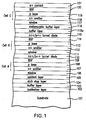
- FIG. 1 depicts the multijunction solar cell after formation of the three subcells A, B and C on a substrate. More particularly, there is shown a first substrate 101, which may be either gallium arsenide (GaAs), germanium (Ge), or other suitable material.
- a nucleation layer 102 such as InGaP 2
- a buffer layer 103 of InGaAs, and an etch stop layer 104 of InAlP 2 are further deposited.
- a contact layer 105 of InGaAs is then deposited on layer 104, and a window layer 106 of InAlP 2 is deposited on the contact layer.
- the subcell A consisting of an n+ emitter layer 107 of InGaP 2 and a p-type base layer 108 of InGaP 2 , is then deposited on the window layer 106.
- the multijunction solar cell structure could be formed by any suitable combination of group III to V elements listed in the periodic table subject to lattice constant and band gap requirements, wherein the group III includes boron (B), aluminum (Al), gallium (Ga), indium (In), and thallium (T).
- the group IV includes carbon (C), silicon (Si), germanium (Ge), and tin (Sn).
- the group V includes nitrogen (N), phosphorous (P), arsenic (As), antimony (Sb), and bismuth (Bi).
- the substrate 101 is gallium arsenide
- the emitter layer 107 is composed of InGa(Al)P 2
- the base layer is composed of InGa(Al)P 2 .
- the use of parenthesis in the formula is standard nomenclature to indicate that the amount of aluminum may vary from 0 to 30%.
- BSF back surface field
- the BSF layer 109 drives minority carriers from the region near the base/BSF interface surface to minimize the effect of recombination loss.
- a BSF layer 109 reduces recombination loss at the backside of the solar subcell A and thereby reduces the recombination in the base.
- a sequence of heavily doped p-type such as AlGaAs
- n-type layers 110 such as InGaP 2
- tunnel diode which is a circuit element to connect cell A to cell B.
- a window layer 111 of n++ InAlP 2 is deposited on top of the tunnel diode layers 110 .
- the window layer 111 used in the subcell B also operates to reduce the recombination loss.
- the window layer 111 also improves the passivation of the cell surface of the underlying junctions. It should be apparent to one skilled in the art that additional layer(s) may be added or deleted in the cell structure without departing from the scope of the present invention.
- the layers of cell B are deposited: the emitter layer 112, and the p-type base layer 113. These layers are preferably composed of InGaP 2 for the emitter and either GaAs or In 0.015 GaAs for the base, respectively, although any other suitable materials consistent with lattice constant and band gap requirements may be used as well.
- a BSF layer 114 of p+ type AlGaAs which performs the same function as the BSF layer 109.
- a p++/n++ tunnel diode 115 is deposited over the BSF layer 114 similar to the layers 110, again forming a circuit element to connect cell B to cell C.
- a buffer layer 115a preferably InGaAs, is deposited over the tunnel diode 115, with a thickness of about 1.0 micron.
- a metamorphic buffer layer 116 is then deposited over the buffer layer 115a.
- the layer 116 is preferably a compositionally step-graded composition of InGaAlAs deposited as a series of layers with monotonically changing lattice constant that provides a transition in lattice constant from cell B to subcell C.
- the bandgap of layer 116 is 1.5 ev constant with a value slightly greater than the bandgap of the middle cell B.
- the step grade contains nine compositionally graded steps with each step layer having a thickness of 0.25 micron.
- the interlayer is composed of InGaAlAs, with monotonically changing lattice constant.
- n+ window layer 117 is deposited on top of the metamorphic buffer layer 116 .
- the window layer 117 improves the passivation of the cell surface of the underlying junctions. Additional layers may be provided without departing from the scope of the present invention.
- the layers of subcell C are deposited; the n-type emitter layer 118 and the p type base layer 119.
- the emitter layer is composed of GaInAs and the base layer is composed of GaInAs with about a 1.0 ev bandgap, although any other semiconductor materials with suitable lattice constant and band gap requirements may be used as well.
- a back surface field (BSF) layer 120 preferably composed of GaInAsP, is deposited.
- a p+ contact layer 121 Over or on top of the BSF layer 120 is deposited a p+ contact layer 121, preferably of p+ type InGaAs.
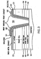
- FIG. 2 is a cross-sectional view of the structure of FIG. 1 after the process step of a via 150 being etched from the top surface of the deposited layers 102 through 121 by dry or wet chemical processes to the substrate 101.
- FIG. 3 is a cross-sectional view of the solar cell structure of FIG. 2 after the next sequence of process step according to the present invention including depositing a back metal layer over the p+ contact layer 121, and depositing a dielectric layer 161 in the interior of the via 150 and over a portion of the back metal contact layer. A conductive layer 162 is then deposited in the via 150 and over the dielectric layer 161. The layer 162 serves as a wrap through front contact for the solar cell.
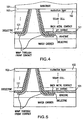
- FIG. 4 is a cross-sectional view of the solar cell of FIG. 3 (how oriented with the substrate 101 at the top of the Figure) after the next process step according to the present invention.
- a wafer carrier or surrogate second substrate is adhered to the "top" side of the solar cell structure, which is now at the bottom of the Figure.
- the surrogate substrate is sapphire about 1000 microns in thickness, and is perforated with holes about 1 mm in diameter, spaced 4 mm apart, to aid in subsequent removal of the substrate.
- FIG. 5 is a cross-sectional view of the solar cell of FIG. 4 after the next process step in which the first substrate 101 is removed by a lapping or grinding process.
- FIG. 6 is a cross-sectional view of the solar cell of FIG. 5 after the next process step according to the present invention in which a cap layer is deposited over a portion of the nucleation layer in the region of the via 150 and metal contact layer is deposited over the cap layer, making electrical contact with the metal layer 161 inside the via 150.
- An antireflective coating (ARC) layer is then applied over the surface of the nucleation layer.
- FIG. 7 is a cross-sectional view of the solar cell of FIG. 6 after the next process step in which an adhesive is applied over the front metal layer and the ARC layer, and a cover glass is adhered to the solar cell structure.
- the surrogate second substrate is then removed by dissolving the adhesive attaching it, or any other suitable technique.
- FIG. 8A and 8B are top and bottom plan views, respectively of a wafer including the solar cell of the present invention.
- Cell 1 of each wafer is illustrated in greater detail with grid lines 501, a bus 502, and circular regions 503 in which a via 150 extends through the wafer such as shown in previous cross-sectional views.
- FIG. 8B depicts the back side contact region 505 and a wrap through front contact region 504 with vias 503 corresponding to those shown in FIG. 8A .
Description
- The present invention relates to the field of solar cell semiconductor devices, and particularly to integrated semiconductor structures including a multijunction solar cell and a conducting via that allows both anode and cathode terminals to be placed on the back side of the cell.
- Photovoltaic cells, also called solar cells, are one of the most important new energy sources that have become available in the past several years. Considerable effort has gone into solar cell development. As a result, solar cells are currently being used in a number of commercial and consumer-oriented applications. While significant progress has been made in this area, the requirement for solar cells to meet the needs of more sophisticated applications has not kept pace with demand. Applications such as satellites used in data communications have dramatically increased the demand for solar cells with improved power and energy conversion characteristics.
- In satellite and other space related applications, the size, mass and cost of a satellite power system are dependent on the power and energy conversion efficiency of the solar cells used. Putting it another way, the size of the payload and the availability of on-board services are proportional to the amount of power provided. Thus, as the payloads become more sophisticated, the design efficiency of solar cells, which act as the power conversion devices for the on-board power systems, become increasingly more important.
- Solar cells are often fabricated in vertical, multijunction structures, and disposed in horizontal arrays, with the individual solar cell connected together in a series. The shape and structure of an array, as well as the number of cells it contains, are determined in part by the desired output voltage and current.
- Inverted metamorphic solar cell structures such as described in
U.S. Patent No. 6,951,819 , the paper of M.W. Wanless et al., Lattice Mismatched Approaches for High Performance, III - V Photovoltaic Energy Converters (Conference Proceedings of the 31st IEEE Photovoltaic Specialists Conference, Jan. 3-7, 2005, IEEE Press, 2005), andU.S. Patent No. 8,536,445 , present an important development in future commercial solar cell products. - Since a solar cell is fabricated as a vertical, multijunction structure, one electrical contact is usually placed on the top surface of the cell, and the other contact on the bottom of the cell, to avoid internal interconnections which may affect reliability and cost. A variety of designs are also known in which both contacts are placed on one side of the cell, including as represented in
U.S. Patent Application 2006/0231130 - Prior to the present invention, there has not been a inverted metamorphic solar cell with both anode and cathode contacts on the same side of the cell as claimed in
claim 1. - The present invention provides a multijunction solar cell having a front side surface and a back side surface including a first solar subcell adjacent the front side surface having a first band gap; a second solar subcell disposed over the first subcell and having a second band gap smaller than said first band gap; a grading interlayer disposed over the second subcell and having a third band gap greater than the second band gap; and a third solar subcell adjacent the back side surface and disposed over the interlayer, the third subcell being lattice mis-matched with respect to said second subcell and having a fourth band gap smaller than the third band gap. As claimed in claim 1 a via is formed in the first, second, and third solar cells with an electrical conductor extending through the via. An insulated contact pad is provided on the back side surface and electrically connected to the conductor to form a first terminal of the solar cell on the back side surface. A second terminal is formed on the back side surface by a metal layer making contact with a contact layer on the back side.
- These and other features and advantages of this invention will be better and more fully appreciated by reference to the following detailed description when considered in conjunction with the accompanying drawings, wherein:
-
FIG. 1 is an enlarged cross-sectional view of a solar cell structure at the end of the process steps of forming a multijunction solar cell on a first substrate; -
FIG. 2 is a cross-sectional view of the structure ofFIG. 1 with a via etched to the first substrate; -
FIG. 3 is a cross-sectional view of the solar cell structure ofFIG. 2 after the next process step according to the present invention including depositing a dielectric layer and a conductive layer in the via; -
FIG. 4 is a cross-sectional view of the solar cell ofFIG. 3 after the next process step in which a wafer carrier or surrogate second substrate is adhered to the "top" side of the solar cell structure; -
FIG. 5 is a cross-sectional view of the solar cell ofFIG. 4 after the next process step in which the first substrate is removed; -
FIG. 6 is a cross-sectional view of the solar cell ofFIG. 5 after the next process step in which a cap layer and metal contact layer is deposited on the structure; -
FIG. 7 is a cross-sectional view of the solar cell ofFIG. 6 after the next process step in which a cover glass is adhered to the solar cell structure on one side, and the surrogate second substrate removed on the other side; and -
FIG. 8A and8B are top and bottom plan views, respectively, of a wafer including the solar cell of the present invention. -
FIG. 1 depicts the multijunction solar cell after formation of the three subcells A, B and C on a substrate. More particularly, there is shown afirst substrate 101, which may be either gallium arsenide (GaAs), germanium (Ge), or other suitable material. In the case of a Ge substrate, anucleation layer 102 such as InGaP2, is deposited on the substrate. On the substrate, or over thenucleation layer 102 in the case of a Ge substrate, abuffer layer 103 of InGaAs, and anetch stop layer 104 of InAlP2 are further deposited. Acontact layer 105 of InGaAs is then deposited onlayer 104, and awindow layer 106 of InAlP2 is deposited on the contact layer. The subcell A, consisting of ann+ emitter layer 107 of InGaP2 and a p-type base layer 108 of InGaP2, is then deposited on thewindow layer 106. - Although the preferred embodiment utilizes the III - V semiconductor materials described above, the embodiment is only illustrative, and it should be noted that the multijunction solar cell structure could be formed by any suitable combination of group III to V elements listed in the periodic table subject to lattice constant and band gap requirements, wherein the group III includes boron (B), aluminum (Al), gallium (Ga), indium (In), and thallium (T). The group IV includes carbon (C), silicon (Si), germanium (Ge), and tin (Sn). The group V includes nitrogen (N), phosphorous (P), arsenic (As), antimony (Sb), and bismuth (Bi).
- In the preferred embodiment, the
substrate 101 is gallium arsenide, theemitter layer 107 is composed of InGa(Al)P2, and the base layer is composed of InGa(Al)P2. The use of parenthesis in the formula is standard nomenclature to indicate that the amount of aluminum may vary from 0 to 30%. - On top of the
base layer 108 is deposited a p+ type back surface field ("BSF")layer 109 of InGaAlP which is used to reduce recombination loss. - The
BSF layer 109 drives minority carriers from the region near the base/BSF interface surface to minimize the effect of recombination loss. In other words, aBSF layer 109 reduces recombination loss at the backside of the solar subcell A and thereby reduces the recombination in the base. - On top of the
BSF layer 109 is deposited a sequence of heavily doped p-type (such as AlGaAs) and n-type layers 110 (such as InGaP2) which forms a tunnel diode which is a circuit element to connect cell A to cell B. - On top of the tunnel diode layers 110 a
window layer 111 of n++ InAlP2 is deposited. Thewindow layer 111 used in the subcell B also operates to reduce the recombination loss. Thewindow layer 111 also improves the passivation of the cell surface of the underlying junctions. It should be apparent to one skilled in the art that additional layer(s) may be added or deleted in the cell structure without departing from the scope of the present invention. - On top of the
window layer 111 the layers of cell B are deposited: theemitter layer 112, and the p-type base layer 113. These layers are preferably composed of InGaP2 for the emitter and either GaAs or In0.015GaAs for the base, respectively, although any other suitable materials consistent with lattice constant and band gap requirements may be used as well. - On top of the cell B is deposited a
BSF layer 114 of p+ type AlGaAs which performs the same function as theBSF layer 109. A p++/n++ tunnel diode 115 is deposited over theBSF layer 114 similar to thelayers 110, again forming a circuit element to connect cell B to cell C.A buffer layer 115a, preferably InGaAs, is deposited over thetunnel diode 115, with a thickness of about 1.0 micron. Ametamorphic buffer layer 116 is then deposited over thebuffer layer 115a. Thelayer 116 is preferably a compositionally step-graded composition of InGaAlAs deposited as a series of layers with monotonically changing lattice constant that provides a transition in lattice constant from cell B to subcell C. The bandgap oflayer 116 is 1.5 ev constant with a value slightly greater than the bandgap of the middle cell B. - In one embodiment, as suggested in the Wanless et al. paper, the step grade contains nine compositionally graded steps with each step layer having a thickness of 0.25 micron. In the preferred embodiment, the interlayer is composed of InGaAlAs, with monotonically changing lattice constant.
- On top of the
metamorphic buffer layer 116 anothern+ window layer 117 is deposited. Thewindow layer 117 improves the passivation of the cell surface of the underlying junctions. Additional layers may be provided without departing from the scope of the present invention. - On top of the
window layer 117 the layers of subcell C are deposited; the n-type emitter layer 118 and the ptype base layer 119. In the preferred embodiment, the emitter layer is composed of GaInAs and the base layer is composed of GaInAs with about a 1.0 ev bandgap, although any other semiconductor materials with suitable lattice constant and band gap requirements may be used as well. - On top of the
base layer 119 of subcell C a back surface field (BSF)layer 120, preferably composed of GaInAsP, is deposited. - Over or on top of the
BSF layer 120 is deposited ap+ contact layer 121, preferably of p+ type InGaAs. -
FIG. 2 is a cross-sectional view of the structure ofFIG. 1 after the process step of a via 150 being etched from the top surface of the depositedlayers 102 through 121 by dry or wet chemical processes to thesubstrate 101. -
FIG. 3 is a cross-sectional view of the solar cell structure ofFIG. 2 after the next sequence of process step according to the present invention including depositing a back metal layer over thep+ contact layer 121, and depositing adielectric layer 161 in the interior of the via 150 and over a portion of the back metal contact layer. Aconductive layer 162 is then deposited in the via 150 and over thedielectric layer 161. Thelayer 162 serves as a wrap through front contact for the solar cell. -
FIG. 4 is a cross-sectional view of the solar cell ofFIG. 3 (how oriented with thesubstrate 101 at the top of the Figure) after the next process step according to the present invention. A wafer carrier or surrogate second substrate is adhered to the "top" side of the solar cell structure, which is now at the bottom of the Figure. In the preferred embodiment, the surrogate substrate is sapphire about 1000 microns in thickness, and is perforated with holes about 1 mm in diameter, spaced 4 mm apart, to aid in subsequent removal of the substrate. -
FIG. 5 is a cross-sectional view of the solar cell ofFIG. 4 after the next process step in which thefirst substrate 101 is removed by a lapping or grinding process. -
FIG. 6 is a cross-sectional view of the solar cell ofFIG. 5 after the next process step according to the present invention in which a cap layer is deposited over a portion of the nucleation layer in the region of the via 150 and metal contact layer is deposited over the cap layer, making electrical contact with themetal layer 161 inside the via 150. An antireflective coating (ARC) layer is then applied over the surface of the nucleation layer. -
FIG. 7 is a cross-sectional view of the solar cell ofFIG. 6 after the next process step in which an adhesive is applied over the front metal layer and the ARC layer, and a cover glass is adhered to the solar cell structure. On the other side, the surrogate second substrate is then removed by dissolving the adhesive attaching it, or any other suitable technique. -
FIG. 8A and8B are top and bottom plan views, respectively of a wafer including the solar cell of the present invention. InFIG. 8A ,Cell 1 of each wafer is illustrated in greater detail withgrid lines 501, abus 502, andcircular regions 503 in which a via 150 extends through the wafer such as shown in previous cross-sectional views. -
FIG. 8B depicts the backside contact region 505 and a wrap throughfront contact region 504 withvias 503 corresponding to those shown inFIG. 8A .
Claims (5)
- A multijunction solar cell having a front surface and a back surface, said solar cell comprising:
a sequence of layers (102-121) of semiconductor material that forms at least two cells of a multijunction solar cell, including:a via (150) extending from the top surface (Fig. 8a) of said sequence of layers (102-121) to the back surface (Fig. 8b);a back metal contact layer over the last layer (121) of the sequence of layers;a layer of dielectric material (161) circumferentially around the inside surface of the via (150) and over a portion of the back metal contact layer;a conductive layer (162) over said layer of dielectric material (161) extending throughout the via (150) and over a portion of the layer of dielectric material (161);a front metal grid (501) on the front surface of the solar cell electrically connected to said conductive layer (162). - The solar cell of claim 1, wherein the back contact metal layer comprises a bal side contact region (505), and the conductive layer (162) comprises a wrap through front contact region (504).
- The solar cell of claim 1, wherein said sequence of layers of semiconductor material comprises a first solar subcell (cell A) having a first band gap; a second solar subcell (cell B) over said first subcell having a second band gap smaller than said first band gap; a grading interlayer (114) over said second subcell having a third band gap larger than said second band gap; a third solar subcell (cell C) having a fourth band gap smaller than said second band gap such that said third subcell is lattice mis-matched with respect to said second subcell.
- The solar cell as defined in claim 3, wherein said first solar subcell (cell A) is composed of an InGa(Al)P emitter region and an InGa(Al)P base region, and said second solar subcell (cell B) is composed of an InGaP2 emitter region and an In0.015GaAs base region.
- The solar cell as defined in claim 3, wherein the grading interlayer (113) is composed of a plurality of layers of InGaAlAs with monotonically increasing lattice constant.
Applications Claiming Priority (2)
| Application Number | Priority Date | Filing Date | Title |
|---|---|---|---|
| US11/701,741 US20080185038A1 (en) | 2007-02-02 | 2007-02-02 | Inverted metamorphic solar cell with via for backside contacts |
| EP07020333A EP1953828B1 (en) | 2007-02-02 | 2007-10-17 | Inverted metamorphic solar cell with via for backside contacts |
Related Parent Applications (2)
| Application Number | Title | Priority Date | Filing Date |
|---|---|---|---|
| EP07020333A Division EP1953828B1 (en) | 2007-02-02 | 2007-10-17 | Inverted metamorphic solar cell with via for backside contacts |
| EP07020333.6 Division | 2007-10-17 |
Publications (3)
| Publication Number | Publication Date |
|---|---|
| EP2290699A2 EP2290699A2 (en) | 2011-03-02 |
| EP2290699A3 EP2290699A3 (en) | 2014-06-25 |
| EP2290699B1 true EP2290699B1 (en) | 2018-11-21 |
Family
ID=39427698
Family Applications (2)
| Application Number | Title | Priority Date | Filing Date |
|---|---|---|---|
| EP07020333A Active EP1953828B1 (en) | 2007-02-02 | 2007-10-17 | Inverted metamorphic solar cell with via for backside contacts |
| EP10010911.5A Active EP2290699B1 (en) | 2007-02-02 | 2007-10-17 | Inverted metamorphic solar cell with via for backside contacts |
Family Applications Before (1)
| Application Number | Title | Priority Date | Filing Date |
|---|---|---|---|
| EP07020333A Active EP1953828B1 (en) | 2007-02-02 | 2007-10-17 | Inverted metamorphic solar cell with via for backside contacts |
Country Status (4)
| Country | Link |
|---|---|
| US (1) | US20080185038A1 (en) |
| EP (2) | EP1953828B1 (en) |
| JP (1) | JP5512086B2 (en) |
| CN (1) | CN101237007B (en) |
Families Citing this family (81)
| Publication number | Priority date | Publication date | Assignee | Title |
|---|---|---|---|---|
| FR2894990B1 (en) | 2005-12-21 | 2008-02-22 | Soitec Silicon On Insulator | PROCESS FOR PRODUCING SUBSTRATES, IN PARTICULAR FOR OPTICS, ELECTRONICS OR OPTOELECTRONICS AND SUBSTRATE OBTAINED BY SAID PROCESS |
| US20090078309A1 (en) * | 2007-09-24 | 2009-03-26 | Emcore Corporation | Barrier Layers In Inverted Metamorphic Multijunction Solar Cells |
| US20090078310A1 (en) * | 2007-09-24 | 2009-03-26 | Emcore Corporation | Heterojunction Subcells In Inverted Metamorphic Multijunction Solar Cells |
| US10381501B2 (en) | 2006-06-02 | 2019-08-13 | Solaero Technologies Corp. | Inverted metamorphic multijunction solar cell with multiple metamorphic layers |
| US20100186804A1 (en) * | 2009-01-29 | 2010-07-29 | Emcore Solar Power, Inc. | String Interconnection of Inverted Metamorphic Multijunction Solar Cells on Flexible Perforated Carriers |
| US20100229926A1 (en) | 2009-03-10 | 2010-09-16 | Emcore Solar Power, Inc. | Four Junction Inverted Metamorphic Multijunction Solar Cell with a Single Metamorphic Layer |
| US20100229913A1 (en) * | 2009-01-29 | 2010-09-16 | Emcore Solar Power, Inc. | Contact Layout and String Interconnection of Inverted Metamorphic Multijunction Solar Cells |
| US9117966B2 (en) | 2007-09-24 | 2015-08-25 | Solaero Technologies Corp. | Inverted metamorphic multijunction solar cell with two metamorphic layers and homojunction top cell |
| US20100122724A1 (en) | 2008-11-14 | 2010-05-20 | Emcore Solar Power, Inc. | Four Junction Inverted Metamorphic Multijunction Solar Cell with Two Metamorphic Layers |
| US10170656B2 (en) | 2009-03-10 | 2019-01-01 | Solaero Technologies Corp. | Inverted metamorphic multijunction solar cell with a single metamorphic layer |
| US9634172B1 (en) | 2007-09-24 | 2017-04-25 | Solaero Technologies Corp. | Inverted metamorphic multijunction solar cell with multiple metamorphic layers |
| US20100047959A1 (en) * | 2006-08-07 | 2010-02-25 | Emcore Solar Power, Inc. | Epitaxial Lift Off on Film Mounted Inverted Metamorphic Multijunction Solar Cells |
| US20100203730A1 (en) * | 2009-02-09 | 2010-08-12 | Emcore Solar Power, Inc. | Epitaxial Lift Off in Inverted Metamorphic Multijunction Solar Cells |
| US20100093127A1 (en) * | 2006-12-27 | 2010-04-15 | Emcore Solar Power, Inc. | Inverted Metamorphic Multijunction Solar Cell Mounted on Metallized Flexible Film |
| US20110041898A1 (en) * | 2009-08-19 | 2011-02-24 | Emcore Solar Power, Inc. | Back Metal Layers in Inverted Metamorphic Multijunction Solar Cells |
| US20100233838A1 (en) * | 2009-03-10 | 2010-09-16 | Emcore Solar Power, Inc. | Mounting of Solar Cells on a Flexible Substrate |
| US10381505B2 (en) | 2007-09-24 | 2019-08-13 | Solaero Technologies Corp. | Inverted metamorphic multijunction solar cells including metamorphic layers |
| US8895342B2 (en) | 2007-09-24 | 2014-11-25 | Emcore Solar Power, Inc. | Heterojunction subcells in inverted metamorphic multijunction solar cells |
| US20090155952A1 (en) * | 2007-12-13 | 2009-06-18 | Emcore Corporation | Exponentially Doped Layers In Inverted Metamorphic Multijunction Solar Cells |
| US20100012175A1 (en) | 2008-07-16 | 2010-01-21 | Emcore Solar Power, Inc. | Ohmic n-contact formed at low temperature in inverted metamorphic multijunction solar cells |
| US20090272430A1 (en) * | 2008-04-30 | 2009-11-05 | Emcore Solar Power, Inc. | Refractive Index Matching in Inverted Metamorphic Multijunction Solar Cells |
| US20090272438A1 (en) * | 2008-05-05 | 2009-11-05 | Emcore Corporation | Strain Balanced Multiple Quantum Well Subcell In Inverted Metamorphic Multijunction Solar Cell |
| US20090288703A1 (en) * | 2008-05-20 | 2009-11-26 | Emcore Corporation | Wide Band Gap Window Layers In Inverted Metamorphic Multijunction Solar Cells |
| US9287438B1 (en) * | 2008-07-16 | 2016-03-15 | Solaero Technologies Corp. | Method for forming ohmic N-contacts at low temperature in inverted metamorphic multijunction solar cells with contaminant isolation |
| US20100012174A1 (en) * | 2008-07-16 | 2010-01-21 | Emcore Corporation | High band gap contact layer in inverted metamorphic multijunction solar cells |
| US8263853B2 (en) * | 2008-08-07 | 2012-09-11 | Emcore Solar Power, Inc. | Wafer level interconnection of inverted metamorphic multijunction solar cells |
| US7741146B2 (en) | 2008-08-12 | 2010-06-22 | Emcore Solar Power, Inc. | Demounting of inverted metamorphic multijunction solar cells |
| US8330036B1 (en) * | 2008-08-29 | 2012-12-11 | Seoijin Park | Method of fabrication and structure for multi-junction solar cell formed upon separable substrate |
| US8236600B2 (en) * | 2008-11-10 | 2012-08-07 | Emcore Solar Power, Inc. | Joining method for preparing an inverted metamorphic multijunction solar cell |
| US20100122764A1 (en) * | 2008-11-14 | 2010-05-20 | Emcore Solar Power, Inc. | Surrogate Substrates for Inverted Metamorphic Multijunction Solar Cells |
| EP2356689A4 (en) * | 2008-11-26 | 2013-11-20 | Microlink Devices Inc | Solar cell with a backside via to contact the emitter layer |
| US20100139755A1 (en) * | 2008-12-09 | 2010-06-10 | Twin Creeks Technologies, Inc. | Front connected photovoltaic assembly and associated methods |
| US7785989B2 (en) | 2008-12-17 | 2010-08-31 | Emcore Solar Power, Inc. | Growth substrates for inverted metamorphic multijunction solar cells |
| US10541349B1 (en) | 2008-12-17 | 2020-01-21 | Solaero Technologies Corp. | Methods of forming inverted multijunction solar cells with distributed Bragg reflector |
| US9018521B1 (en) | 2008-12-17 | 2015-04-28 | Solaero Technologies Corp. | Inverted metamorphic multijunction solar cell with DBR layer adjacent to the top subcell |
| US20100147366A1 (en) * | 2008-12-17 | 2010-06-17 | Emcore Solar Power, Inc. | Inverted Metamorphic Multijunction Solar Cells with Distributed Bragg Reflector |
| US7960201B2 (en) * | 2009-01-29 | 2011-06-14 | Emcore Solar Power, Inc. | String interconnection and fabrication of inverted metamorphic multijunction solar cells |
| US8778199B2 (en) | 2009-02-09 | 2014-07-15 | Emoore Solar Power, Inc. | Epitaxial lift off in inverted metamorphic multijunction solar cells |
| US20100206365A1 (en) * | 2009-02-19 | 2010-08-19 | Emcore Solar Power, Inc. | Inverted Metamorphic Multijunction Solar Cells on Low Density Carriers |
| KR101573934B1 (en) * | 2009-03-02 | 2015-12-11 | 엘지전자 주식회사 | Solar cell and manufacturing mehtod of the same |
| US20100229933A1 (en) * | 2009-03-10 | 2010-09-16 | Emcore Solar Power, Inc. | Inverted Metamorphic Multijunction Solar Cells with a Supporting Coating |
| US9018519B1 (en) | 2009-03-10 | 2015-04-28 | Solaero Technologies Corp. | Inverted metamorphic multijunction solar cells having a permanent supporting substrate |
| US20100282288A1 (en) * | 2009-05-06 | 2010-11-11 | Emcore Solar Power, Inc. | Solar Cell Interconnection on a Flexible Substrate |
| US20100282305A1 (en) * | 2009-05-08 | 2010-11-11 | Emcore Solar Power, Inc. | Inverted Multijunction Solar Cells with Group IV/III-V Hybrid Alloys |
| KR101108474B1 (en) * | 2009-05-14 | 2012-01-31 | 엘지전자 주식회사 | Solar cell |
| CN101958348B (en) * | 2009-07-16 | 2013-01-02 | 晶元光电股份有限公司 | Lateral solar battery device |
| US8263856B2 (en) * | 2009-08-07 | 2012-09-11 | Emcore Solar Power, Inc. | Inverted metamorphic multijunction solar cells with back contacts |
| US8115097B2 (en) | 2009-11-19 | 2012-02-14 | International Business Machines Corporation | Grid-line-free contact for a photovoltaic cell |
| US8187907B1 (en) | 2010-05-07 | 2012-05-29 | Emcore Solar Power, Inc. | Solder structures for fabrication of inverted metamorphic multijunction solar cells |
| CN102290454A (en) * | 2010-06-21 | 2011-12-21 | 杜邦太阳能有限公司 | Multi-electrode solar panel |
| US20130306141A1 (en) * | 2011-05-20 | 2013-11-21 | Panasonic Corporation | Multi-junction compound solar cell, mutli-junction compound solar battery, and method for manufacturing same |
| DE102011115659A1 (en) * | 2011-09-28 | 2013-03-28 | Osram Opto Semiconductors Gmbh | Photovoltaic semiconductor chip |
| US9263611B2 (en) | 2011-11-17 | 2016-02-16 | Solar Junction Corporation | Method for etching multi-layer epitaxial material |
| WO2013152104A1 (en) * | 2012-04-06 | 2013-10-10 | Solar Junction Corporation | Multi-junction solar cells with through-via contacts |
| US9059366B2 (en) * | 2012-04-23 | 2015-06-16 | The Aerospace Corporation | Bonding of photovoltaic device to covering material |
| US9142615B2 (en) | 2012-10-10 | 2015-09-22 | Solar Junction Corporation | Methods and apparatus for identifying and reducing semiconductor failures |
| US10153388B1 (en) | 2013-03-15 | 2018-12-11 | Solaero Technologies Corp. | Emissivity coating for space solar cell arrays |
| US10553738B2 (en) * | 2013-08-21 | 2020-02-04 | Sunpower Corporation | Interconnection of solar cells in a solar cell module |
| DE102014102029A1 (en) * | 2014-02-18 | 2015-08-20 | Osram Opto Semiconductors Gmbh | Process for the production of semiconductor devices and semiconductor device |
| US11563133B1 (en) | 2015-08-17 | 2023-01-24 | SolAero Techologies Corp. | Method of fabricating multijunction solar cells for space applications |
| US20220102564A1 (en) * | 2015-08-17 | 2022-03-31 | Solaero Technologies Corp. | Four junction metamorphic multijunction solar cells for space applications |
| FR3041475B1 (en) * | 2015-09-23 | 2018-03-02 | Commissariat Energie Atomique | METHOD FOR MANUFACTURING STRUCTURES FOR PHOTOVOLTAIC CELL |
| US9935209B2 (en) * | 2016-01-28 | 2018-04-03 | Solaero Technologies Corp. | Multijunction metamorphic solar cell for space applications |
| US10403778B2 (en) * | 2015-10-19 | 2019-09-03 | Solaero Technologies Corp. | Multijunction solar cell assembly for space applications |
| US10270000B2 (en) | 2015-10-19 | 2019-04-23 | Solaero Technologies Corp. | Multijunction metamorphic solar cell assembly for space applications |
| US10256359B2 (en) | 2015-10-19 | 2019-04-09 | Solaero Technologies Corp. | Lattice matched multijunction solar cell assemblies for space applications |
| US9985161B2 (en) | 2016-08-26 | 2018-05-29 | Solaero Technologies Corp. | Multijunction metamorphic solar cell for space applications |
| US10361330B2 (en) | 2015-10-19 | 2019-07-23 | Solaero Technologies Corp. | Multijunction solar cell assemblies for space applications |
| US10090420B2 (en) * | 2016-01-22 | 2018-10-02 | Solar Junction Corporation | Via etch method for back contact multijunction solar cells |
| US11316053B2 (en) * | 2016-08-26 | 2022-04-26 | Sol Aero Technologies Corp. | Multijunction solar cell assembly |
| CN105633178B (en) * | 2016-03-21 | 2017-10-17 | 无锡携创新能源科技有限公司 | A kind of back contacts technique cell piece and preparation method thereof |
| CN105826407B (en) * | 2016-03-21 | 2017-10-17 | 无锡携创新能源科技有限公司 | A kind of back contacts technique battery component and preparation method thereof |
| US10263134B1 (en) | 2016-05-25 | 2019-04-16 | Solaero Technologies Corp. | Multijunction solar cells having an indirect high band gap semiconductor emitter layer in the upper solar subcell |
| US9680035B1 (en) * | 2016-05-27 | 2017-06-13 | Solar Junction Corporation | Surface mount solar cell with integrated coverglass |
| GB2552097B (en) * | 2016-05-27 | 2019-10-16 | Solar Junction Corp | Surface mount solar cell with integrated coverglass |
| US10636926B1 (en) | 2016-12-12 | 2020-04-28 | Solaero Technologies Corp. | Distributed BRAGG reflector structures in multijunction solar cells |
| US20190181289A1 (en) | 2017-12-11 | 2019-06-13 | Solaero Technologies Corp. | Multijunction solar cells |
| EP3821475A4 (en) * | 2018-07-13 | 2022-03-23 | Array Photonics, Inc. | Dual-depth via device and process for large back contact solar cells |
| DE102019006094B4 (en) * | 2019-08-29 | 2021-04-22 | Azur Space Solar Power Gmbh | Two-stage hole etching process |
| DE102019006091B4 (en) * | 2019-08-29 | 2022-03-17 | Azur Space Solar Power Gmbh | Multiple solar cell with back-contacted front side |
| DE102019006097A1 (en) * | 2019-08-29 | 2021-03-04 | Azur Space Solar Power Gmbh | Passivation process for a through hole in a semiconductor wafer |
Family Cites Families (55)
| Publication number | Priority date | Publication date | Assignee | Title |
|---|---|---|---|---|
| US2004104A (en) * | 1932-07-30 | 1935-06-11 | American Can Co | Container |
| US4001864A (en) * | 1976-01-30 | 1977-01-04 | Gibbons James F | Semiconductor p-n junction solar cell and method of manufacture |
| US4283589A (en) * | 1978-05-01 | 1981-08-11 | Massachusetts Institute Of Technology | High-intensity, solid-state solar cell |
| US4338480A (en) * | 1980-12-29 | 1982-07-06 | Varian Associates, Inc. | Stacked multijunction photovoltaic converters |
| JPS63211773A (en) * | 1987-02-27 | 1988-09-02 | Mitsubishi Electric Corp | Compound semiconductor sloar cell |
| US4759803A (en) * | 1987-08-07 | 1988-07-26 | Applied Solar Energy Corporation | Monolithic solar cell and bypass diode system |
| US5332572A (en) * | 1988-11-10 | 1994-07-26 | Iowa State University Research Foundation | Method for protection of swine against pleuropneumonia |
| DE68923061T2 (en) * | 1988-11-16 | 1995-11-09 | Mitsubishi Electric Corp | Solar cell. |
| US5053083A (en) * | 1989-05-08 | 1991-10-01 | The Board Of Trustees Of The Leland Stanford Junior University | Bilevel contact solar cells |
| US5019177A (en) * | 1989-11-03 | 1991-05-28 | The United States Of America As Represented By The United States Department Of Energy | Monolithic tandem solar cell |
| JPH04223378A (en) * | 1990-12-25 | 1992-08-13 | Sharp Corp | Solar cell |
| US5425816A (en) * | 1991-08-19 | 1995-06-20 | Spectrolab, Inc. | Electrical feedthrough structure and fabrication method |
| US5342453A (en) * | 1992-11-13 | 1994-08-30 | Midwest Research Institute | Heterojunction solar cell |
| US5376185A (en) * | 1993-05-12 | 1994-12-27 | Midwest Research Institute | Single-junction solar cells with the optimum band gap for terrestrial concentrator applications |
| JP3360919B2 (en) * | 1993-06-11 | 2003-01-07 | 三菱電機株式会社 | Method of manufacturing thin-film solar cell and thin-film solar cell |
| JP3169497B2 (en) * | 1993-12-24 | 2001-05-28 | 三菱電機株式会社 | Solar cell manufacturing method |
| US6147296A (en) * | 1995-12-06 | 2000-11-14 | University Of Houston | Multi-quantum well tandem solar cell |
| EP0881694A1 (en) * | 1997-05-30 | 1998-12-02 | Interuniversitair Micro-Elektronica Centrum Vzw | Solar cell and process of manufacturing the same |
| US6281426B1 (en) * | 1997-10-01 | 2001-08-28 | Midwest Research Institute | Multi-junction, monolithic solar cell using low-band-gap materials lattice matched to GaAs or Ge |
| US6482672B1 (en) * | 1997-11-06 | 2002-11-19 | Essential Research, Inc. | Using a critical composition grading technique to deposit InGaAs epitaxial layers on InP substrates |
| US5944913A (en) * | 1997-11-26 | 1999-08-31 | Sandia Corporation | High-efficiency solar cell and method for fabrication |
| JP2000036609A (en) * | 1998-05-15 | 2000-02-02 | Canon Inc | Manufacture of solar cell, manufacture of thin-film semiconductor, method for separating thin-film semiconductor, and method for forming semiconductor |
| US6278054B1 (en) * | 1998-05-28 | 2001-08-21 | Tecstar Power Systems, Inc. | Solar cell having an integral monolithically grown bypass diode |
| US6103970A (en) * | 1998-08-20 | 2000-08-15 | Tecstar Power Systems, Inc. | Solar cell having a front-mounted bypass diode |
| DE19845658C2 (en) * | 1998-10-05 | 2001-11-15 | Daimler Chrysler Ag | Solar cell with bypass diode |
| US6239354B1 (en) * | 1998-10-09 | 2001-05-29 | Midwest Research Institute | Electrical isolation of component cells in monolithically interconnected modules |
| US6300557B1 (en) * | 1998-10-09 | 2001-10-09 | Midwest Research Institute | Low-bandgap double-heterostructure InAsP/GaInAs photovoltaic converters |
| JP3657143B2 (en) * | 1999-04-27 | 2005-06-08 | シャープ株式会社 | Solar cell and manufacturing method thereof |
| DE19921545A1 (en) * | 1999-05-11 | 2000-11-23 | Angew Solarenergie Ase Gmbh | Solar cell and method for producing such |
| US6252287B1 (en) * | 1999-05-19 | 2001-06-26 | Sandia Corporation | InGaAsN/GaAs heterojunction for multi-junction solar cells |
| US6162987A (en) * | 1999-06-30 | 2000-12-19 | The United States Of America As Represented By The United States Department Of Energy | Monolithic interconnected module with a tunnel junction for enhanced electrical and optical performance |
| US6635507B1 (en) * | 1999-07-14 | 2003-10-21 | Hughes Electronics Corporation | Monolithic bypass-diode and solar-cell string assembly |
| US6340788B1 (en) * | 1999-12-02 | 2002-01-22 | Hughes Electronics Corporation | Multijunction photovoltaic cells and panels using a silicon or silicon-germanium active substrate cell for space and terrestrial applications |
| DE10008583A1 (en) * | 2000-02-24 | 2001-09-13 | Osram Opto Semiconductors Gmbh | Production of an optically transparent substrate comprises epitaxially growing a substrate layer on a substrate, connecting the substrate layer to the side with an optically transparent layer, and removing the substrate |
| US7339109B2 (en) * | 2000-06-20 | 2008-03-04 | Emcore Corporation | Apparatus and method for optimizing the efficiency of germanium junctions in multi-junction solar cells |
| US7119271B2 (en) * | 2001-10-12 | 2006-10-10 | The Boeing Company | Wide-bandgap, lattice-mismatched window layer for a solar conversion device |
| US20030070707A1 (en) * | 2001-10-12 | 2003-04-17 | King Richard Roland | Wide-bandgap, lattice-mismatched window layer for a solar energy conversion device |
| US6864414B2 (en) * | 2001-10-24 | 2005-03-08 | Emcore Corporation | Apparatus and method for integral bypass diode in solar cells |
| US6680432B2 (en) * | 2001-10-24 | 2004-01-20 | Emcore Corporation | Apparatus and method for optimizing the efficiency of a bypass diode in multijunction solar cells |
| US6660928B1 (en) * | 2002-04-02 | 2003-12-09 | Essential Research, Inc. | Multi-junction photovoltaic cell |
| US20060162768A1 (en) * | 2002-05-21 | 2006-07-27 | Wanlass Mark W | Low bandgap, monolithic, multi-bandgap, optoelectronic devices |
| US8067687B2 (en) * | 2002-05-21 | 2011-11-29 | Alliance For Sustainable Energy, Llc | High-efficiency, monolithic, multi-bandgap, tandem photovoltaic energy converters |
| US6768141B2 (en) * | 2002-08-23 | 2004-07-27 | Agilent Technologies, Inc. | Heterojunction bipolar transistor (HBT) having improved emitter-base grading structure |
| JP2004095669A (en) * | 2002-08-29 | 2004-03-25 | Toyota Motor Corp | Photoelectric conversion element |
| US7122733B2 (en) * | 2002-09-06 | 2006-10-17 | The Boeing Company | Multi-junction photovoltaic cell having buffer layers for the growth of single crystal boron compounds |
| US7071407B2 (en) * | 2002-10-31 | 2006-07-04 | Emcore Corporation | Method and apparatus of multiplejunction solar cell structure with high band gap heterojunction middle cell |
| US7335835B2 (en) * | 2002-11-08 | 2008-02-26 | The Boeing Company | Solar cell structure with by-pass diode and wrapped front-side diode interconnection |
| US6818928B2 (en) * | 2002-12-05 | 2004-11-16 | Raytheon Company | Quaternary-ternary semiconductor devices |
| AU2003297649A1 (en) * | 2002-12-05 | 2004-06-30 | Blue Photonics, Inc. | High efficiency, monolithic multijunction solar cells containing lattice-mismatched materials and methods of forming same |
| JP4401649B2 (en) * | 2002-12-13 | 2010-01-20 | キヤノン株式会社 | Manufacturing method of solar cell module |
| US7812249B2 (en) * | 2003-04-14 | 2010-10-12 | The Boeing Company | Multijunction photovoltaic cell grown on high-miscut-angle substrate |
| US7286583B2 (en) * | 2003-08-22 | 2007-10-23 | The Board Of Trustees Of The University Of Illinois | Semiconductor laser devices and methods |
| US20050211291A1 (en) * | 2004-03-23 | 2005-09-29 | The Boeing Company | Solar cell assembly |
| US20060231130A1 (en) * | 2005-04-19 | 2006-10-19 | Sharps Paul R | Solar cell with feedthrough via |
| US20080029151A1 (en) * | 2006-08-07 | 2008-02-07 | Mcglynn Daniel | Terrestrial solar power system using III-V semiconductor solar cells |
-
2007
- 2007-02-02 US US11/701,741 patent/US20080185038A1/en not_active Abandoned
- 2007-10-17 EP EP07020333A patent/EP1953828B1/en active Active
- 2007-10-17 EP EP10010911.5A patent/EP2290699B1/en active Active
- 2007-12-20 CN CN2007103022341A patent/CN101237007B/en active Active
-
2008
- 2008-02-01 JP JP2008022765A patent/JP5512086B2/en not_active Expired - Fee Related
Non-Patent Citations (2)
| Title |
|---|
| COOLEY W T ET AL: "PHOTOVOLTAIC ARRAY SPACE POWER FLIGHT EXPERIMENT PLUS DIAGNOSTICS (PASP+) MODULES", AEROSPACE POWER. SAN DIEGO, AUG 3 - 7, 1992; [PROCEEDINGS OF THE INTERSOCIETY ENERGY CONVERSION ENGINEERING CONFERENCE (IECEC)], NEW YORK, IEEE, US, vol. 1, 3 August 1992 (1992-08-03), pages 1.295 - 1.301, XP000366026, ISBN: 978-0-7803-0693-6 * |
| YOO H ET AL: "Development of coplanar back contact for large area, thin, GaAs/Ge solar cells", PROCEEDINGS OF THE PHOTOVOLTAIC SPECIALISTS CONFERENCE. LAS VEGAS, OCT. 7 - 11, 19; [PROCEEDINGS OF THE PHOTOVOLTAIC SPECIALISTS CONFERENCE], NEW YORK, IEEE, US, vol. CONF. 22, 7 October 1991 (1991-10-07), pages 1463 - 1468, XP010039150, ISBN: 978-0-87942-636-1, DOI: 10.1109/PVSC.1991.169447 * |
Also Published As
| Publication number | Publication date |
|---|---|
| EP1953828B1 (en) | 2011-05-11 |
| EP1953828A1 (en) | 2008-08-06 |
| EP2290699A3 (en) | 2014-06-25 |
| JP5512086B2 (en) | 2014-06-04 |
| JP2008193089A (en) | 2008-08-21 |
| US20080185038A1 (en) | 2008-08-07 |
| EP2290699A2 (en) | 2011-03-02 |
| CN101237007B (en) | 2011-07-13 |
| CN101237007A (en) | 2008-08-06 |
Similar Documents
| Publication | Publication Date | Title |
|---|---|---|
| EP2290699B1 (en) | Inverted metamorphic solar cell with via for backside contacts | |
| US11677037B2 (en) | Metamorphic layers in multijunction solar cells | |
| EP1788628B1 (en) | Via structures in solar cells with bypass diode | |
| EP2073276B1 (en) | Exponentially doped layers in inverted metamorphic multijunction solar cells | |
| EP2040309A2 (en) | Thin inverted metamorphic multijunction solar cells with rigid support | |
| US8263853B2 (en) | Wafer level interconnection of inverted metamorphic multijunction solar cells | |
| EP1936703A2 (en) | Inverted metamorphic solar cell with bypass diode | |
| US20090078309A1 (en) | Barrier Layers In Inverted Metamorphic Multijunction Solar Cells | |
| US20100282307A1 (en) | Multijunction Solar Cells with Group IV/III-V Hybrid Alloys for Terrestrial Applications | |
| EP2148378B1 (en) | Barrier layers in inverted metamorphic multijunction solar cells |
Legal Events
| Date | Code | Title | Description |
|---|---|---|---|
| PUAI | Public reference made under article 153(3) epc to a published international application that has entered the european phase |
Free format text: ORIGINAL CODE: 0009012 |
|
| 17P | Request for examination filed |
Effective date: 20100927 |
|
| AC | Divisional application: reference to earlier application |
Ref document number: 1953828 Country of ref document: EP Kind code of ref document: P |
|
| AK | Designated contracting states |
Kind code of ref document: A2 Designated state(s): DE ES FR IT |
|
| PUAL | Search report despatched |
Free format text: ORIGINAL CODE: 0009013 |
|
| AK | Designated contracting states |
Kind code of ref document: A3 Designated state(s): DE ES FR IT |
|
| RIC1 | Information provided on ipc code assigned before grant |
Ipc: H01L 31/072 20120101ALI20140522BHEP Ipc: H01L 21/461 20060101ALI20140522BHEP Ipc: H01L 21/302 20060101ALI20140522BHEP Ipc: H01L 31/0224 20060101AFI20140522BHEP |
|
| RAP1 | Party data changed (applicant data changed or rights of an application transferred) |
Owner name: SOLAERO TECHNOLOGIES CORP. |
|
| 17Q | First examination report despatched |
Effective date: 20160601 |
|
| GRAP | Despatch of communication of intention to grant a patent |
Free format text: ORIGINAL CODE: EPIDOSNIGR1 |
|
| INTG | Intention to grant announced |
Effective date: 20180615 |
|
| GRAS | Grant fee paid |
Free format text: ORIGINAL CODE: EPIDOSNIGR3 |
|
| GRAA | (expected) grant |
Free format text: ORIGINAL CODE: 0009210 |
|
| AC | Divisional application: reference to earlier application |
Ref document number: 1953828 Country of ref document: EP Kind code of ref document: P |
|
| AK | Designated contracting states |
Kind code of ref document: B1 Designated state(s): DE ES FR IT |
|
| REG | Reference to a national code |
Ref country code: DE Ref legal event code: R096 Ref document number: 602007056943 Country of ref document: DE |
|
| PG25 | Lapsed in a contracting state [announced via postgrant information from national office to epo] |
Ref country code: ES Free format text: LAPSE BECAUSE OF FAILURE TO SUBMIT A TRANSLATION OF THE DESCRIPTION OR TO PAY THE FEE WITHIN THE PRESCRIBED TIME-LIMIT Effective date: 20181121 |
|
| PG25 | Lapsed in a contracting state [announced via postgrant information from national office to epo] |
Ref country code: IT Free format text: LAPSE BECAUSE OF FAILURE TO SUBMIT A TRANSLATION OF THE DESCRIPTION OR TO PAY THE FEE WITHIN THE PRESCRIBED TIME-LIMIT Effective date: 20181121 |
|
| REG | Reference to a national code |
Ref country code: DE Ref legal event code: R097 Ref document number: 602007056943 Country of ref document: DE |
|
| PLBE | No opposition filed within time limit |
Free format text: ORIGINAL CODE: 0009261 |
|
| STAA | Information on the status of an ep patent application or granted ep patent |
Free format text: STATUS: NO OPPOSITION FILED WITHIN TIME LIMIT |
|
| 26N | No opposition filed |
Effective date: 20190822 |
|
| PGFP | Annual fee paid to national office [announced via postgrant information from national office to epo] |
Ref country code: FR Payment date: 20190913 Year of fee payment: 13 |
|
| PG25 | Lapsed in a contracting state [announced via postgrant information from national office to epo] |
Ref country code: FR Free format text: LAPSE BECAUSE OF NON-PAYMENT OF DUE FEES Effective date: 20201031 |
|
| PGFP | Annual fee paid to national office [announced via postgrant information from national office to epo] |
Ref country code: DE Payment date: 20230830 Year of fee payment: 17 |