EP2288033A1 - Successive approximation analog-to-digital converter - Google Patents
Successive approximation analog-to-digital converter Download PDFInfo
- Publication number
- EP2288033A1 EP2288033A1 EP10172719A EP10172719A EP2288033A1 EP 2288033 A1 EP2288033 A1 EP 2288033A1 EP 10172719 A EP10172719 A EP 10172719A EP 10172719 A EP10172719 A EP 10172719A EP 2288033 A1 EP2288033 A1 EP 2288033A1
- Authority
- EP
- European Patent Office
- Prior art keywords
- analog
- value
- digital
- digital converter
- phase
- Prior art date
- Legal status (The legal status is an assumption and is not a legal conclusion. Google has not performed a legal analysis and makes no representation as to the accuracy of the status listed.)
- Granted
Links
Images




Classifications
-
- H—ELECTRICITY
- H03—ELECTRONIC CIRCUITRY
- H03M—CODING; DECODING; CODE CONVERSION IN GENERAL
- H03M1/00—Analogue/digital conversion; Digital/analogue conversion
- H03M1/10—Calibration or testing
- H03M1/1071—Measuring or testing
- H03M1/1076—Detection or location of converter hardware failure, e.g. power supply failure, open or short circuit
-
- H—ELECTRICITY
- H03—ELECTRONIC CIRCUITRY
- H03M—CODING; DECODING; CODE CONVERSION IN GENERAL
- H03M1/00—Analogue/digital conversion; Digital/analogue conversion
- H03M1/10—Calibration or testing
- H03M1/1071—Measuring or testing
- H03M1/109—Measuring or testing for DC performance, i.e. static testing
-
- H—ELECTRICITY
- H03—ELECTRONIC CIRCUITRY
- H03M—CODING; DECODING; CODE CONVERSION IN GENERAL
- H03M1/00—Analogue/digital conversion; Digital/analogue conversion
- H03M1/12—Analogue/digital converters
- H03M1/34—Analogue value compared with reference values
- H03M1/38—Analogue value compared with reference values sequentially only, e.g. successive approximation type
- H03M1/46—Analogue value compared with reference values sequentially only, e.g. successive approximation type with digital/analogue converter for supplying reference values to converter
- H03M1/466—Analogue value compared with reference values sequentially only, e.g. successive approximation type with digital/analogue converter for supplying reference values to converter using switched capacitors
- H03M1/468—Analogue value compared with reference values sequentially only, e.g. successive approximation type with digital/analogue converter for supplying reference values to converter using switched capacitors in which the input S/H circuit is merged with the feedback DAC array
Definitions
- the present invention generally relates to the field of the analog-to-digital converters. More particularly, the present invention concerns a successive-approximation analog-to-digital converter.
- analog-to-digital converter is a device for converting an analog signal into a digital signal represented by a determined number of bits.
- successive-approximation analog-to-digital converter wherein the bits of the digital signal are successively determined one by one, typically from the most significant bit to the least significant bit.
- a successive-approximation analog-to-digital converter comprising a first plurality of capacitors for converting a digital signal into an analog signal and comprising a second plurality of capacitors.
- the second plurality of capacitors is used for performing a self-calibration for compensating variations of capacitance values of the first plurality of capacitors, thus improving the accuracy of the analog-to-digital converter.
- the present invention relates to an analog-to-digital converter as defined in the enclosed claim 1 and in preferred embodiments thereof described in the dependent claims from 2 to 8.
- the Applicant has recognized that a successive-approximation analog-to-digital converter according to the present invention can be used itself for performing a test for controlling its correct operation.
- the analog-to-digital converter according to an embodiment of the invention has the advantage of providing not only an indication of a failure or degradation of the operation of the analog-to-digital converter (for example, of a component of the converter), but also of providing the position of the failure or degradation within the analog-to-digital converter (that is which is the failed or degraded component).
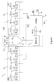
- an analog-to-digital converter is shown according to a first embodiment of the invention.
- the analog-to-digital converter 1 is such to have a normal operation mode wherein it has the function of performing the conversion of an input analog value V in (for example, an analog voltage value) into an output digital value S N quantizated with N bit; the normal operation mode comprises a sampling phase and a subsequent conversion phase.
- the analog-to-digital converter 1 further has a test operation mode wherein it has the function of performing a test of the operation of the analog-to-digital converter 1 itself; the test operation mode comprises a configuration phase and a subsequent phase of execution of the successive-approximation algorithm, as it will be described in more detail afterwards in the section relating to the operation of the analog-to-digital converter 1.
- the test operation mode can be activated when the analog-to-digital converter 1 is inactive, that is when the analog-to-digital converter 1 is not performing a conversion from analog to digital in the normal operation mode.
- the analog-to-digital converter 1 comprises:
- the normal or test operation mode can be referred in the same way to the analog-to-digital converter 1 or to the controller 50; therefore it will be indicated as normal or test operation mode of the analog-to-digital converter 1 or of the controller 50.
- the first generator 20 of the first embodiment of the invention is implemented with a plurality of capacitors - indicated in the following with sampling capacitors - 21, 22, ...24, 25 having equal capacitance values and having respective first terminals connected to each other in order to form a common terminal which coincides (see Figure 1 ) with the output terminal 2 of the first generator 20 (this common terminal will be indicated in the following with "common terminal 2").
- the first generator 20 further comprises a plurality of switches 26, 27, ...28, 29 adapted to switch, as a function of the configuration signal S3, among a first, a second and a third positionfor connecting the second terminals (that is the ones different from the first terminals connected each other to the common terminal 2) of the plurality of sampling capacitors 21, 22, ...24, 25 to the input analog value V in , to a low reference voltage VrefL or to a high reference voltage VrefH (higher than the low reference voltage VrefL) respectively.
- the plurality of sampling capacitors 21, 22, ...24, 25 and the plurality of switches 26, 27, ...28, 29 controlled by the configuration signal S3 have the function of generating at the output terminal 2 the first analog value V x at the end of the configuration phase of the test operation mode.
- the plurality of sampling capacitors 21, 22, ...24, 25 and the plurality of switches 26, 27, ...28, 29 controlled by the configuration signal S3 also have the function of performing a digital-to-analog conversion of the digital value S N (corresponding to the sampled input analog value V in ) when the analog-to-digital converter 1 is such to operate during the conversion phase of the normal operation mode: therefore, in the conversion phase of the normal operation mode the plurality of sampling capacitors 21, 22, ...24, 25 and the plurality of switches 26, 27, ...28, 29 controlled by the configuration signal S3 are such to operate as a capacitive-type digital-to-analog converter for converting the digital value S N into an analog value.
- the digital-to-analog converter 40 of the first embodiment of the invention is of a capacitive type, that is it's implemented with a plurality of capacitors - indicated in the following with reference capacitors - 41, 42, ...44, 45 having equal capacitance values and having respective first terminals connected to each other in order to form a common terminal that coincides (see Figure 1 ) with the output terminal 3 of the digital-to-analog converter 40 (therefore such common terminal will be indicated in the following with "common terminal 3").
- the plurality of reference capacitors 41, 42, ...44, 45 (having equal capacitances values) is equivalent to a corresponding plurality of capacitors 41', 42', ...44', 45' with capacitance having half values with respect to the former capacitance, starting from capacitor 45' to capacitor 41', wherein the capacitor 45' is associated to the most significant bit of the successive-approximation algorithm, while the capacitor 41' is associated to the least significant bit of the successive-approximation algorithm; for example, the capacitance of the capacitor 44' is half the capacitance of capacitor 45' and the capacitance of the capacitor 41' is half the capacitance of capacitor 42'.
- the digital-to-analog converter 40 further comprises a plurality of switches 46, 47, ...48, 49 adapted to switch, as a function of the control signal S1, between a first and a second position for connecting the second terminals (that is the ones different from the common terminal 3) of the plurality of reference capacitors 41, 42, ...44, 45 to a low reference voltage VrefL' or to a high reference voltage VrefH' (greater than the low reference voltage VrefL') respectively, when the analog-to-digital converter 1 is such to operate in the phase of execution of the successive-approximation algorithm of the test operation mode; moreover, the switches 46, 47, ...48, 49 are such to be configured (by means of the control signal S1) for connecting the second terminals of the plurality of reference capacitors 41, 42, ...44, 45 to the low
- the second generator 30 comprises a comparator 31 having a sampling input terminal 37 which is connected to the common terminal 2, comprises a reference input terminal 38 which is connected to the common terminal 3 and comprises an output terminal 39, such to generate a logic value '1' when the value on the sampling input terminal 37 is smaller than the value of reference terminal 38 and such to generate a logic value '0' when the value on the sampling input terminal 37 is greater than the value of the reference terminal 38.
- the second generator 30 further comprises switches 35, 36 controlled by a switching signal S2 and a N-bit register 32 connected to the output terminal 39 for storing the output digital value S N .
- the controller 50 is such to generate the configuration signal S3 to control:
- the controller 50 is such to generate the control signal S1 for:
- the controller 50 is such to generate the switching signal S2 for controlling the switches 35 and 36 in the closed position when the analog-to-digital converter 1 is such to operate in the steps a), b) of the configuration phase of the test operation mode, in the open position when the analog-to-digital converter 1 is such to operate in the steps c), d) of the configuration phase of the test operation mode, and in the open position when the analog-to-digital converter 1 is such to operate in the phase of execution of the successive-approximation algorithm of the test operation mode, as it will be explained more in detail afterwards.
- Switches 35 and 36 are such to switch, depending on the switching signal S2 generated by the controller 50, between the closed position wherein the input terminals are connected to a common reference voltage V cm and the open position.
- Figure 3 schematically shows the pattern of the voltage signal S6 (solid line) at the common terminal 2 and of the voltage signal S7 (broken line) at the common terminal 3 when the analog-to-digital converter 1 is such to operate in the test mode.
- the voltage signal S6 is first equal to the common reference voltage V cm , then it has a variation from the value of the common reference voltage V cm to the first voltage analog value V x and finally is equal to the first voltage analog value V x , while the voltage signal S7 is first equal to the common reference voltage V cm and then it converges to the first voltage analog value V x .
- the analog-to-digital converter 1 operates first according to a sampling phase and then according to a conversion phase.
- Switches 46, 47, ...48, 49 connect the second terminals of the reference capacitors 41, 42, ...44, 45 to a fixed configuration, both during the sampling phase and during the conversion phase of the normal operation mode; for example, all the second reference terminals 41, 42, ...44, 45 are connected to the low reference voltage VrefL'.
- the impedance of the input sampling terminal 37 of the comparator 31 and the impedance of the input reference terminal 38 of the comparator 31 are of the capacitive type.
- the controller 50 During the sampling phase of the normal operation mode, the controller 50 generates the switching signal S2 which closes the switches 35, 36 and generates the configuration signal S3 which connects switches 26, 27, ...28, 29 to the input voltage V in analog value; consequently, the voltage at the ends of the sampling capacitors 21, 22, ...24, 25 is equal to the difference between the common reference voltage V cm and the analog value of the input voltage V in . Since in the example it is supposed that the switches 46, 47, ...48, 49 connect the second terminals of the reference capacitors 41, 42, ...44, 45 to the low reference voltage VrefL', the voltage at the ends of the reference capacitors 41, 42, ...44, 45 is equal to the difference between the common reference voltage V cm and the low reference voltage VrefL'.
- the controller 50 During the conversion phase of the normal operation mode, the controller 50 generates a switching signal S2 which opens the switches 35 and 36 and carries out a successive-approximation algorithm, generating the configuration signal S3 which connects the switches 26, 27 ...28, 29 to the high reference voltage VrefH or to the low reference voltage VrefL. Since this successive-approximation algorithm is known to the person skilled in the art, it will not be described in detail.
- the difference between the voltage of the common terminal 2 and the voltage of the common terminal 3 is smaller than the minimum resolution of the analog-to-digital converter.
- the second terminals of the sampling capacitors 21, 22, ...24, 25 are connected (by means of the switches 26, 27, ...28, 29) to the high reference voltage VrefH or to the low reference voltage VrefL, as a function of the value of the digital signal S N .
- the impedance of the reference terminal 3 of the comparator 31 is of a capacitive type
- the voltage of the common terminal 3 of the plurality of reference capacitors 41, 42, 43, 44 is equal to the common reference voltage V cm .
- the N-bit register 32 stores the N-bit digital value corresponding to the digital conversion of the input analog value V in .
- the analog-to-digital converter 1 in the test operation mode comprises a configuration phase and a subsequent phase of execution of the successive-approximation algorithm: the configuration phase is comprised between times t 0 and t 5 (excluded) shown in Figure 3 , while the phase of execution of the successive-approximation algorithm is comprised between times t 5 and t 8 . Moreover it is supposed a correct operation of the analog-to-digital converter 1, that is there are no failures or degradations of components inside the analog-to-digital converter 1.
- the controller 50 In the configuration phase of the test operation mode the controller 50 generates a sequence of values of the configuration signal S3 for configuring at least two of the switches 26, 27, ...28, 29 in order to connect the second terminals of at least two of the respective sampling capacitors 21, 22, ... 23, 24 to the high reference voltage VrefH or to the low reference voltage VrefL (while the second terminals of other sampling capacitors are floating).
- the controller 50 generates a sequence of values of the configuration signal S3 for configuring the two switches 26, 27 in order to connect the second terminals of the two sampling capacitors 21, 22 to the high reference voltage VrefH or to the low reference voltage VrefL (while the second terminals of the other sampling capacitors 24, 25 are floating) and the controller 50 generates the sequence of values of the configuration signal S3 according to the steps a), b), c), d) explained afterwards.
- switches 46, 47, ...48, 49 connect the second terminals of the reference capacitors 41, 42, ...44, 45 to a fixed configuration; advantageously, all the second terminals of the reference capacitors 41, 42, ...44 are connected to the low reference voltage VrefL' and the capacitor 45 to the high reference voltage VrefH', so that in the phase of execution of the successive-approximation algorithm of the test mode it is possible to detect a variation of the voltage signal S6 leading the voltage signal S6 to a value both greater and smaller than the value of the voltage signal S7 ( Figure 3 shows the example wherein between times t 3 and t 4 of the configuration phase occurs a variation of the voltage signal S6 leading the voltage signal S6 to a value greater than the value of the voltage signal S7).
- the configuration phase of the test mode comprises the following steps a), b), c), d).
- Steps a), b) have the purpose to generate part of the sequence of values of the configuration signal S3 to initialize the values of the voltage at the ends of the sampling capacitors 21 and 22.
- Step a) is comprised between times t 0 and t 1 (excluded) shown in Figure 3 .
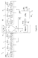
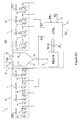
- the controller 50 At time to the controller 50 generates first values of the sequence of the configuration signal S3 which configures the switches 26 and 27 to connect the second terminal of the capacitor 21 to the high reference voltage VrefH and to connect the second terminal of the capacitor 22 to the low reference voltage VrefL, as schematically shown in Figure 2A . Moreover, the controller 50 generates the switching signal S2 which closes the switches 35 and 36 (see Figure 2A ): in this way the common terminal 2, the input sampling terminal 37, the common terminal 3 and the input reference terminal 38 are connected to the common reference voltage V cm .
- the value of the voltage signal S6 at the common terminal 2 and the value of voltage signal S7 at the common terminal 3 are equal to the common reference voltage V cm (as shown in Figure 3 at time t 0 ), the value of voltage at the ends of the capacitor 21 is equal to the difference between the high reference voltage VrefH and the common reference voltage V cm and the voltage value at the ends of the capacitor 22 is equal to the difference between the common reference voltage V cm and the high reference voltage VrefL.
- Step b) is comprised between times t 1 and t 2 (excluded) shown in Figure 3 .
- the controller 50 At time t 1 the controller 50 generates second values of the sequence of the configuration signal S3 which performs a first inversion of voltage of the second terminals of sampling capacitors 21, 22, that is it configures the switches 26 and 27 connecting the second terminal of the capacitor 21 to the low reference voltage VrefL and connects the second terminal of the capacitor 22 to the high reference voltage VrefH, as schematically shown in Figure 2B . Moreover, the controller 50 generates the switching signal S2 which keeps closed the switches 35 and 36 (see Figure 2B ).
- the value of the voltage signal S6 at the common terminal 2 and value of the voltage signal S7 at the common terminal 3 is equal to the common reference voltage V cm (as shown in Figure 3 at time t 1 )
- the value of the voltage at the ends of the capacitor 21 is equal to the difference between the common reference voltage V cm and the low reference voltage VrefL
- the value of voltage at the ends of the capacitor 22 is equal to the difference between the common reference voltage V cm and the high reference voltage VrefH.
- Step c) is comprised between times t 2 and t 3 (excluded) shown in Figure 3 .
- the controller 50 At time t 2 , the controller 50 generates the switching signal S2 which opens the switches 35 and 36 (see Figure 2C ), keeping the same configuration of step b) for switches 26 and 27.
- the voltage signal S6 at the common terminal 2 and the voltage signal S7 at the common terminal 3 keep the value of the common reference voltage V cm , as shown in Figure 3 .
- Step d) is comprised between times t 3 and t 4 shown in Figure 3 .
- Step d) has the purpose to generate at the common terminal 2 the first analog value V x , which will be calculated afterwards.
- the controller 50 At time t 3 the controller 50 generates third values of the sequence of configuration signal S3 which performs a second inversion of the voltage of the second terminals of the sampling capacitors 21, 22, that is it configures switches 26 and 27 connecting the second terminal of the capacitor 21 to the high reference voltage VrefH and connecting the second terminal of the capacitor 22 to the low reference voltage VrefL, as schematically shown in Figure 2D . Moreover, the controller 50 generates the switching signal S2 which keeps open the switches 35 and 36 (see Figure 2D ).
- the voltage signal S6 at the common terminal 2 has a variation from the value of the common reference voltage V cm to the first voltage analog value V x (as shown in Figure 3 ), while the voltage signal S7 at the common terminal 3 keeps the value of the common reference voltage V cm (as shown in Figure 3 ).
- the voltage value at the ends of the capacitor 21 is equal to the difference between the first voltage analog value V x (whose value will be calculated in the following) and the high reference voltage VrefH and the voltage value at the ends of the capacitor 22 is equal to the difference between the first voltage analog value V x and the low reference voltage VrefL.
- the capacitance values C 21 and C 22 have some tolerances (for example caused by the manufacturing process) and thus the capacitance values C 21 and C 22 are slightly different: anyway in this case it is possible to foresee a range of possible capacitance values C 21 and C 22 . Consequently, in the real case and in the hypothesis of a correct operation of the analog-to-digital converter 1, the first voltage analog value V x can take a range of correct values comprised between V x,min and V x,max and this range is centered around the common reference voltage V cm , where V x,min and V x,max are known values which depend on the tolerances of the capacitance values C 21 and C 22 .
- this first voltage analog value V x is a value which will be used at the end of step e) of the phase of execution of the successive-approximation algorithm of the test mode for performing the test of the operation of analog-to-digital converter 1, by means of a comparison of the digital value S N stored into register 32 with respect to one or more pre-defined values (that are known), wherein the digital value S N corresponds to the digital conversion of the first voltage analog value V x .
- steps a)-d) perform the initialization and the configuration of a pair of the plurality of the sampling capacitors 21, 22, ..., 24, 25.
- the voltage value at the common terminal 2 remains substantially equal to the first voltage analog value V x also in the subsequent times of the phase of execution of the successive-approximation algorithm of the test operation mode, as shown in Figure 3 between times t 5 and t 8 ; similarly, at the same times comprised between t 5 and t 8 the second terminals of the capacitors 21 and 22 remain connected as described in step d) (that is the second terminal of the capacitor 21 remains connected to the high reference voltage VrefH and the second terminal of the capacitor 22 remains connected to the low reference voltage VrefL).
- the phase of execution of the successive-approximation algorithm consists of step e) comprised between times t 5 and t 8 shown in Figure 3 .
- step e) a successive-approximation algorithm is carried out on the plurality of reference capacitors 41, 42, ...44, 45 of the digital-to-analog converter 40, wherein the controller 50 generates the switching signal S2 which keeps open the switches 35, 36 and carries out (times t 5 , t 6 , t 7 , t 8 ) the successive-approximation algorithm, generating the control signal S1 in order to connect the switches 46, 47, ...48, 49 to the high reference voltage VrefH' or to the low reference voltage VrefL'.
- the digital value S N stored into the register 32 corresponds to the digital conversion of the first analog value V x , that is the digital value S N is substantially equal the digital conversion of the common reference voltage V cm .
- the first analog value V x takes correct values in a range comprised between V x,min and V x,max and is centered around the common reference voltage value V cm , wherein V x,min and V x,max are known values depending on the tolerances of the sampling capacitors 21, 22, ..., 24, 25 (as previously explained in the formula for calculating V x ): consequently, the digital value S N takes correct values in a range comprised between S N,min and S N,max wherein S N,min is a known value corresponding to the digital conversion of V x,min and S N,max is a known value corresponding to the digital conversion of V x,max .
- the second terminals of the reference capacitors 41, 42, ...44, 45 at the end of the phase of execution of the successive-approximation algorithm of the test operation mode are connected (by means of the switches 46, 47, ...48, 49) to the high reference voltage VrefH' or to the low reference voltage VrefL', as determined by the successive-approximation algorithm carried out on the plurality of reference capacitors 41, 42, ...44, 45.
- the first voltage analog value V x is substantially different from the common reference voltage value V cm , that is the first voltage analog value V x is outside the range comprised between V x,min and V x,max and is centered around the common reference voltage V cm value. Consequently, the digital value S N takes values that are outside the range of values between S N,min and S N,max .
- step b) the voltage of the capacitor 22 is not charged to the value (VrefH-V cm ) and keeps the value (VrefL-V cm ) of step a).
- V x ⁇ 1 V cm + VrefH - VrefL * C 21 / C 21 + C 22
- V x1 in formula (4a) is different from the value V x of the formula (4): therefore the value V x1 will be outside the range of the correct values comprised between V x,min and V x,max and thus the digital value S N1 (corresponding to the digital conversion of V x1 ) will be outside the range of the correct values comprised between S N,min and S N,max (wherein S N,min is the digital conversion of V x,min and S N,max is the digital conversion of V x,max ).
- the failure is an open circuit between the sampling capacitor 22 and the low reference voltage VrefL.
- the voltage of the capacitor 21 is not charged to value (V x -VrefL) and keeps the value (V cm -VrefH) of step c).
- V x ⁇ 2 V cm + VrefH - VrefL
- V cm (VrefH+VrefL)/2
- the value V x2 in the formula (4c) is different from the value V x of the formula (4): the value V x2 will be outside the range of the correct values comprised between V x,min and V x,max and thus the digital value S N2 (corresponding to the digital conversion of V x2 ) will be outside the range of the correct values comprised between S N,min and S N,max (wherein S N,min is the digital conversion of V x,min and S N,max is the digital conversion of V x,max ).
- V f VrefH * RL / RF + RL + VrefL * RH / RH + RL
- V x ⁇ 3 V cm + VrefH * C 21 - C 22 * C 22 + C 21 + C 22 * V f - C 21 * VrefL / C 22 + C 21
- the value V x3 of the formula (4c) is different from the value V x of the formula (4): therefore the value V x3 will be outside the range of the correct values comprised between V x,min and V x,max and thus the digital value S N3 (corresponding to the digital conversion of V x3 ) will be outside the range of the correct values comprised between S N,min and S N,max (wherein S N,min is the digital conversion of V x,min and S N,max is the digital conversion of V x,max ).
- step b) the voltage of the capacitor 22 is not charged to the value (VrefH-V cm ), but it's equal to the value (V f -V cm ), wherein V f has the value indicated in the formula (5c).
- V x ⁇ 4 V cm + VrefL * C 22 - C 21 * C 22 + C 21 + C 21 * VrefH - C 22 * V f / C 22 + C 21
- the value V x4 in the formula (4d) is different from the value V x of the formula (4): therefore the value of V x4 will be outside the range of the correct values comprised between V x,min and V x,max and thus the digital value S N4 (corresponding to the digital conversion of V x4 ) will be outside the range of the correct values comprised between S N,min and S N,max (wherein S N,min is the digital conversion of V x,min and S N,max is the digital conversion of V x,max ).
- the failure is an open circuit between the common terminal 2 of the sampling capacitor 22 and the sampling input terminal 37 of comparator 31. In this case, the sampling capacitor 22 is not charged and it's necessary to consider the parasitic capacitance (indicated with C p ) seen from the sampling input terminal 37 of the comparator 31.
- V x ⁇ 5 V cm + C 21 * VrefH - VrefL / C p + C 21
- the value V x5 of the formula (4e) is thus different from the value V x of formula (4): therefore the value V x5 will be outside the range of correct values comprised between V x,min and V x,max and thus the digital value S N5 (corresponding to the digital conversion of V x5 ) will be outside the range of correct values comprised between S N,min and S N,max (wherein S N,min is the digital conversion of V x,min and S N,max is the digital conversion of V x,max ).
- the second terminals of the sampling capacitors not used for performing the test are connected at a constant value voltage (for example, VrefL).
- VrefL a constant value voltage
- the controller 50 further comprises an output terminal 51 (see Figures 1 and 2A-D ) for generating, as a function of the digital value S N , an alarm signal S5 indicating the correct operation (for example, a low logic value) of the analog-to-digital converter 1 or indicating a failure (for example, a high logic value) of at least one component in the analog-to-digital converter 1 or indicating a degradation of the performance of the analog-to-digital converter 1.
- an alarm signal S5 indicating the correct operation (for example, a low logic value) of the analog-to-digital converter 1 or indicating a failure (for example, a high logic value) of at least one component in the analog-to-digital converter 1 or indicating a degradation of the performance of the analog-to-digital converter 1.
- the controller 50 receives the digital value S N stored into the register 32, receives the values S N,min and S N,max (for examples, they are read from a memory connected to the controller 50 or from a memory inside the controller 50, or such values are written at hardware level into the controller 50), performs a comparison between the digital value S N and the range defined between S N,min and S N,max , checks if the digital value S N is comprised into said range and generates the alarm signal S5 (in the example, the high logic value) in case that the digital value S N is outside said range.
- the alarm signal S5 in the example, the high logic value
- a microprocessor is connected to the analog-to-digital converter 1 and reads the digital value stored into the register 32, receives the values S N,min and S N,max (for example, they are read from a memory connected to the processor), performs a comparison between the digital value S N and the range defined between S N,min and S N,max , checks if the digital value S N is comprised within said range and generates the alarm signal S5 (in the example, the high logic value) in case the digital value S N is outside said range.
- the phase of configuration and execution of the successive-approximation algorithm of the test mode is repeated for other pairs (or for all the pairs) of the sampling capacitors, that is for pairs of the sampling capacitors different from the pair 21, 22 of the previous example.
- This allows to determine the position of a failure of at least one of the sampling capacitors 21, 22, ...24, 25.
- the steps a)-e) performed on a first capacitors pair are independent from the steps a)-e) performed on a second capacitors pair: this has the advantage that it is possible to stop the test after completing the test on the first capacitors pair, in order to return to the normal operation mode.Subsequently, it is possible to resume the execution of the test mode on the second capacitors pair, without the necessity of performing again the test mode on the first capacitors pair.
- the phase of configuration and execution of the successive-approximation algorithm of the test mode is performed for a group of sampling capacitors comprising an even number of sampling capacitor greater than or equal to four: this has the advantage of reducing the number of the required switches 26, 27, ..., 28, 29.
- FIG. 4 it is shown an analog-to-digital converter 101 according to a second embodiment of the invention. It should be noted that in Figure 4 blocks, components or modules identical (or similar) are indicated with the same reference numerals of Figure 1 of the first embodiment.
- the analog-to-digital converter 101 further comprises a resistive-type digital-to-analog converter 60 implemented with a resistive divider, that is with a series connection of a plurality of resistors 61, 62,... 64, 64 connected between the high reference voltage VrefH and the low reference voltage VrefL, as schematically shown in Figure 4 .
- the resistive-type digital-to-analog converter 60 comprises an output terminal 63 for providing a third voltage analog value V y comprised between the high reference voltage VrefH and the low reference voltage VrefL by means of a plurality of switches 66, 67, ...68, 69 alternatively closed and connected between the resistors 61, 62, ...64, 65 and the output terminal 63.
- the analog-to-digital converter 101 comprises a third generator 120 (similar to the first generator 20 of the first embodiment of the invention) comprising a plurality of switches 126, 127, ...128, 129 adapted to switch, as a function of the configuration signal S3, among a first, a second, a third, and a fourth position for connecting the second terminals of the plurality of sampling capacitors 21, 22, ...24, 25 to the input analog value V in , to the low reference voltage VrefL, to the high reference voltage VrefH or to the output terminal 63 of digital-to-analog converter 60 respectively.
- a third generator 120 similar to the first generator 20 of the first embodiment of the invention
- switches 126, 127, ...128, 129 adapted to switch, as a function of the configuration signal S3, among a first, a second, a third, and a fourth position for connecting the second terminals of the plurality of sampling capacitors 21, 22, ...24, 25 to the input analog value V in , to the low reference voltage
- the digital-to-analog converter 60 is such to generate at the output terminal 63 at least the third voltage analog value V y as a function of the configuration signal S3, when the analog-to-digital converter 1 is such to operate in the configuration phase of the test operation mode, similarly to what has been explained for the sampling phase of the normal operation mode.
- Figure 4 shows switches 126, 127, ...128, 129 having four possible positions (connection to V in , VrefL, VrefH, output terminal 63), but it's possible to obtain the same operation using the switches 126, 127, ...128, 129 having three possible positions (connection with V in , VrefL, VrefH) and adding another switch for connecting the output terminal 63 to the terminal having the input analog value V in .
- the operation of the analog-to-digital converter 101 according to the second embodiment of the test mode is similar to the operation of the analog-to-digital converter 1 in the normal operation mode, with the following differences:
- the digital value S N stored into the register 32 at the end of the operation of the test mode corresponds to the digital conversion of the third voltage analog value V y .
- the digital value S N stored into the register 32 corresponds to the digital conversion of the third voltage analog value V y , wherein V y can have possible values in a range centered around an ideal value of V y and depending on the tolerances of the resistors 61, 62, ...64, 65 and on the tolerances of the sampling capacitors 21, 22, ...24, 25.
- the ideal value of V y is known because is equal to the voltage value generated at output terminal 63 of the resistive-type digital-to-analog converter 60.
- the third analog value V y has values in a range comprised between V y,min and V y,max and centered around the ideal value of V y , where V y,min and V y,max are known values which depend on the tolerances of the resistors 61, 62, ...64, 65 and on the tolerances of the sampling capacitors (caused, for example, by the manufacturing process): consequently, the digital value S N has values in a range comprised between S N,min ' and S N,max ', wherein S N,min ' has a known value corresponding to the digital conversion of V y,min and S N,max ' is a known value corresponding to the digital conversion of V y,max .
- the second terminals of the sampling capacitors 21, 22, ...24, 25 at the end of the phase of execution of the successive-approximation algorithm of the test operation mode are connected (by means of the switches 126, 127, ...128, 129) to the high reference voltage VrefH or to the low reference voltage VrefL, as determined by the successive-approximation algorithm.
- the third voltage analog value V y is substantially different from the ideal value of V y , that is the third voltage analog value V y is outside the range of correct values comprised between V y,min and V y,max . Consequently, the digital value S N has values which are outside the range of correct values comprised between S N,min and S N,max
- the analog-to-digital converter 101 of the second embodiment of the invention in the test operation mode can detect failures previously indicated in the examples 1-5 and moreover it can detect failures indicated in the following other examples 6-14.
- the failure is a short-circuit of at least one of the resistors 61, 62, ...64, 65.
- each of the third voltage analog values V y generated by the closure of the corresponding switch selected among 66, 67, ...68, 69 is outside the respective range of correct values comprised between V y,min and V y,max ; consequently, each of the digital values S N (corresponding to the digital conversion of the respective third voltage analog value V y ) is outside the respective range of correct values comprised between S N,min ' and S N,max ' (wherein S N,min ' is the digital conversion of the respective V y,min and S N,max ' is the digital conversion of the respective V y,max ).
- the failure is an open circuit of at least one of the resistors 61, 62, ...64, 65.
- the digital-to-analog converter 60 comprises four resistors 61, 62, 64, 65 and that the open-circuited failed resistor is 62.
- the following iterations of the test mode are performed, wherein the controller 50 generates the configuration signal S3 in order to perform the sequential closure of the switches 66, 67, 68, 69:
- the failure is at least one of the resistors 61, 62, ...64, 65 having a resistance value substantially different from the nominal value.
- each of the third voltage analog values V y generated by the closure of the corresponding switch selected among 66, 67, ...68, 69 is shifted of a determined value with respect to the correct value and thus it's outside the respective range of correct values comprised between V y,min and V y,max ; consequently, each digital values S N (corresponding to the digital conversion of the respective voltage analog value V y ) is outside the respective range of correct values comprised between S N,min ' and S N,max ' (wherein S N,min ' is the digital conversion of the respective V y,min and S N,max ' is the digital conversion of the respective V y,max ).
- the failure is a short-circuit of at least one of the plurality of switches 66, 67, ...68, 69.
- a failure its detection is possible performing the test by closing at least another switch (not a failed one) selected among 66, 67, ...68, 69, in order to form a short-circuit of one or more resistors 61, 62, ...64, 65: in this last case the third voltage analog value V y is outside the range of correct values comprised between V y,min and V y,max .
- the digital value S N (corresponding to the digital conversion of the third voltage analog value V y ) is outside the range of correct values comprised between S N,min ' and S N,max ' (wherein S N,min ' is the digital conversion of the respective V y,min and S N,max ' is the digital conversion of the respective V y,max ).
- the failure is an open circuit of at least one of the plurality of switches 66, 67, ...68, 69.
- the sampling capacitors 21, 22, ...24, 25 are not charged to the expected value when the failed open-circuited switch (of the plurality of switches 66, 67, ...68, 69) is closed.
- the digital-to-analog converter 60 comprises four resistors 61, 62, 64, 65 and that the failed open-circuited switch is 67.
- the following iterations of the test mode are performed, wherein the controller 50 generates, for each iteration, the configuration signal S3 for performing the sequential closure of the switches 66, 67, 68, 69:
- the failure is an open-circuit of the switch 35.
- the common terminal 2 of the sampling capacitors 21, 22, ...24, 25 is floating and thus the sampling capacitors 21, 22, ...24, 25 are connected to the parasitic capacitance (indicated with C p ) of the common terminal 2.
- the plurality of sampling capacitors 21, 22, ...24, 25 is charged through the parasitic capacitance C p to the value (Vin-Vg)*C s *C p /(C s +C p ), wherein C s is the capacitance value of the plurality of sampling capacitors 21, 22, ...24, 25, Vg is the voltage applied to the terminal of C p not connected to the common terminal 2.
- the voltage of the common terminal 2 will have the value (Vin-Vg)*C p /(C s +C p ), which is different from the voltage of the common reference V cm : therefore the third voltage analog value V y is outside the range of the correct values comprised between V y,min and V y,max and, consequently, the digital value S N (corresponding to the digital conversion of the third voltage analog value V y ) is outside the range of the correct values.
- the failure is a short-circuit of the switch 35.
- the voltage value of the input terminal 37 of the comparator 31 is always equal to the reference voltage V cm and thus the digital signal S N has always the same value as the selected switch among the plurality of switches 66, 67, ...68, 69 changes.
- the failure is a short-circuit of at least one of the sampling capacitors 21, 22, ...24, 25.
- the voltage value of the common terminal 2 (and thus of the input terminal 37 of the comparator 31) is equal to the high reference voltage VrefH when, during the phase of execution of the successive-approximation algorithm on the plurality of sampling capacitors 21, 22, ...24, 25, a specific bit of the digital signal S N is evaluated: consequently, the comparator 31 generates a low logic value for this specific bit of the digital signal S N .
- the voltage value of the common terminal 2 (and thus of the input terminal 37 of the comparator 31) is equal to the low reference voltage VrefL when, during the phase of execution of the successive-approximation algorithm on the plurality of sampling capacitors 21, 22, ...24, 25, the other bits of the digital signal S N are evaluated: consequently, the comparator 31 generates a high logic value for the other bits of the digital signal S N .
- the comparator 31 is failed. This affects the digital value S N , which is outside the range of correct values comprised between S N,min ' and S N,max '.
- Figure 4 also shows a third embodiment of the invention.
- the digital-to-analog converter 60 in the configuration phase of the test mode, the digital-to-analog converter 60 generates the third voltage analog value V y (similarly to the configuration phase of the second embodiment of the invention), wherein the controller 50 generates the configuration signal S3 for selecting the closure of one of the plurality of switches 66, 67, ...68, 69.
- the controller 50 In the configuration phase of the test mode, it is also performed the sampling of the third voltage analog value V y on the plurality of sampling capacitors 21, 22, ...24, 25 (similarly to the sampling of the input analog signal V in in the sampling phase of the normal operation mode of the first embodiment of the invention), that is wherein the controller 50 generates the configuration signal S3 for connecting the second terminals of the plurality of sampling capacitors 21, 22, ...24, 25 to the third voltage analog value V y and wherein the controller 50 generates the switching signal S2 for closing the switches 35, 36.
- the successive-approximation algorithm is carried out on the plurality of reference capacitors 41, 42, ...44, 45 (similarly to the phase of execution of the successive-approximation algorithm of the first embodiment of the invention) connecting the second terminals of the plurality of reference capacitors 41, 42, ...44, 45 to the low reference voltage VrefL' or to the high reference voltage VrefH', by means of the switches 46, 47, ...48, 49 and the digital value S N (corresponding to the digital conversion of the difference between the voltage signal S106 at the common terminal 2 and the voltage signal S107 at the common terminal 3) is obtained: if the digital value S N has values in a range comprised between S N,min " and S N,max " (wherein S N,min " is a known value corresponding to the digital conversion of the difference between the minimum correct value S106 min of the voltage signal S106 and the value of the voltage signal S107 and S N,max " is a known value corresponding to the digital conversion of the difference between the maximum
- any value of the third voltage analog value V y has a correspondent correct value that is the result of the conversion of the third voltage analog value V y in the condition of no failure inside the analog-to-digital converter 101 and ideal components composing the analog-to-digital converter 101, according to the known operation of a successive-approximation algorithm.
- This result is a binary value corresponding to a configuration of the third generator 120 wherein (for example) bit '1' is associated to one of the sampling capacitors 21,22 ...24,25 connected to the high reference voltage VrefH and bit '0' is associated to one of the sampling capacitors 21,22 ...24,25 connected to the low reference voltage VrefL, with the weight of each bit in the binary word result corresponding to the weight of the related capacitor inside the third generator 120.
- the difference between the voltage signal S106 and the voltage signal S107 is evaluated on the plurality of reference capacitors 41, 42, ...44, 45.
- the change of the voltage signal S106 with respect to the voltage signal S107 is negligible.
- the change of the voltage signal S106 with respect to the voltage signal S107 is not negligible and depends only on the tolerance of the sampling capacitors 21,22 ...24,25 and on the tolerance of the resistors 61, 62, 64, 65, and the difference between the voltage signal S106 and the voltage signal S107 is evaluated with the successive-approximation algorithm carried out on the plurality of reference capacitors 41, 42, ...44, 45.
- the tolerance affecting the components causes a shift of the voltage signal S106 with respect to the voltage signal S107 that is not negligible, but which is known in case the tolerance of the components is known: this known tolerance leads to a maximum S106 max and minimum S106 min correct values for the voltage signal S106 (like in the first embodiment of the invention, even if the two values S106 max and S106 min are different from S6 max and S6 min due to different components - the resistors 61, 62, 64, 65 - involved in the third embodiment and the different related tolerance) and the difference between the voltage signal S106 and the voltage signal S107, which is evaluated with the successive-approximation algorithm carried out on the plurality of reference capacitors 41, 42, ...44, 45, is inside the range of correct values comprised between S N,min " and S N,max" .
- the difference between the voltage signal S106 and the voltage signal S107, which is evaluated with the successive-approximation algorithm carried out on the plurality of reference capacitors 41, 42, ...44, 45, is outside the range of correct values comprised between S N,min " and S N,max ".
- the third embodiment of the invention has the advantage that the range used for checking in the test mode the correct operation of the analog-to-digital converter 101 is always the same as the third voltage analog value V y generated by the digital-to-analog converter 60 at the output terminal 63 changes.
- the programming language used for the program software could be, for example, C or VHDL (Very high-speed integrated circuit Hardware Description Language) or Verilog.
Landscapes
- Engineering & Computer Science (AREA)
- Theoretical Computer Science (AREA)
- Analogue/Digital Conversion (AREA)
Abstract
Description
- The present invention generally relates to the field of the analog-to-digital converters. More particularly, the present invention concerns a successive-approximation analog-to-digital converter.
- It is known that the analog-to-digital converter is a device for converting an analog signal into a digital signal represented by a determined number of bits.
- Specifically, it is known the successive-approximation analog-to-digital converter, wherein the bits of the digital signal are successively determined one by one, typically from the most significant bit to the least significant bit.
- Failures or performance degradation of the components of the analog-to-digital converter can occur.
- It is known a successive-approximation analog-to-digital converter comprising a first plurality of capacitors for converting a digital signal into an analog signal and comprising a second plurality of capacitors. The second plurality of capacitors is used for performing a self-calibration for compensating variations of capacitance values of the first plurality of capacitors, thus improving the accuracy of the analog-to-digital converter.
- Techniques for performing the test of the operation of the analog-to-digital converter by using circuits outside the analog-to-digital converter, which thus have the disadvantage to require a dedicated circuit for performing the test, are also known.
- Therefore it is necessary to guarantee a correct operation of the analog-to-digital converter, especially in applications which require high safety and reliability, such as for example in the automotive field.
- The present invention relates to an analog-to-digital converter as defined in the enclosed claim 1 and in preferred embodiments thereof described in the dependent claims from 2 to 8.
- The Applicant has recognized that a successive-approximation analog-to-digital converter according to the present invention can be used itself for performing a test for controlling its correct operation.
- This has the advantage of not requiring additional circuits external to the analog-to-digital converter and of not requiring complex modifications to the same analog-to-digital converter.
- Moreover, the analog-to-digital converter according to an embodiment of the invention has the advantage of providing not only an indication of a failure or degradation of the operation of the analog-to-digital converter (for example, of a component of the converter), but also of providing the position of the failure or degradation within the analog-to-digital converter (that is which is the failed or degraded component).
- It is also an object of the present invention an integrated circuit as defined in the enclosed claim 9.
- It is also an object of the present invention a system for detecting a failure of a successive-approximation analog-to-digital converter as defined in the enclosed claim 10.
- It is also an object of the present invention a method for testing the operation of an analog-to-digital converter as defined in the enclosed claim 11 and in the preferred embodiment described in the dependent claim 12.
- It is also an object of the present invention a computer program as defined in the enclosed claim 13.
- Further features and the advantages of the invention will be understood from the following description of a preferred embodiment and of its variations given in an illustrative way referring to the enclosed drawings, wherein:
-
Figure 1 schematically shows an analog-to-digital converter according to a first embodiment of the invention; -
Figures 2A ,2B ,2C ,2D schematically show some steps of the test operation mode of the analog-to-digital converter according to the first embodiment of the invention; -
Figure 3 schematically shows a possible pattern of two signals which can be generated in the analog-to-digital converter according to the first embodiment of the invention; -
Figure 4 schematically shows an analog-to-digital converter according to a second and third embodiments of the invention. - With reference to
Figure 1 , an analog-to-digital converter is shown according to a first embodiment of the invention. - The analog-to-digital converter 1 is such to have a normal operation mode wherein it has the function of performing the conversion of an input analog value Vin (for example, an analog voltage value) into an output digital value SN quantizated with N bit; the normal operation mode comprises a sampling phase and a subsequent conversion phase.
- The analog-to-digital converter 1 further has a test operation mode wherein it has the function of performing a test of the operation of the analog-to-digital converter 1 itself; the test operation mode comprises a configuration phase and a subsequent phase of execution of the successive-approximation algorithm, as it will be described in more detail afterwards in the section relating to the operation of the analog-to-digital converter 1. For example, the test operation mode can be activated when the analog-to-digital converter 1 is inactive, that is when the analog-to-digital converter 1 is not performing a conversion from analog to digital in the normal operation mode.
- The analog-to-digital converter 1 comprises:
- a
first generator 20 comprising anoutput terminal 2 and having the function of performing the sampling of the input analog value Vin when the analog-to-digital converter 1 is such to operate in the sampling phase of the normal operation mode, and having the function of performing the conversion from the digital value SN into an analog value when the analog-to-digital converter 1 is such to operate in the conversion phase of the normal operation mode; moreover thefirst generator 20 is such to generate at the output terminal 2 a first analog value (in the following referred with Vx) as a function of a configuration signal S3, when the analog-to-digital converter 1 is such to operate in the configuration phase of the test operation mode, as it will be explained more in detail afterwards in the section relating to the operation of the analog-to-digital converter 1; - a digital-to-
analog converter 40 comprising anoutput terminal 3 for generating an analog value when the analog-to-digital converter 1 is such to operate in normal operation mode; moreover, the digital-to-analog converter 40 is such to generate at the output terminal 3 a second analog value as a function of a control signal S1 when the analog-to-digital converter 1 is such to operate in the phase of execution of the successive-approximation algorithm of the test operation mode, as it will be explained more in detail in the following with reference to the description of the analog-to-digital converter 1 in the test mode. The digital-to-analog converter 40 is used to perform the test of the operation of components inside the analog-to-digital converter 1 (as it will be described more in detail in the following), by means of the execution of a successive-approximation algorithm on the digital-to-analog converter 40 : - a
second generator 30 for receiving an analog value from theoutput terminal 2, an analog value from theoutput terminal 3 and generating a digital value SN by means of a successive-approximation algorithm, when the analog-to-digital converter 1 is such to operate in the conversion phase of the normal operation mode; moreover, thesecond generator 30 is such to receive the first analog value Vx from theoutput terminal 2 of thefirst generator 20, is such to receive the second analog value from theoutput terminal 3 of the digital-to-analog converter 40, is such to perform a comparison between the first analog value Vx and the second analog value and it is such to generate the digital value SN corresponding to the digital conversion of the first analog value Vx by means of a successive-approximation algorithm, when analog-to-digital converter 1 is such to operate in the execution phase of the successive-approximation algorithm of the test operation mode, as it will explained more in detail hereinafter; - a
controller 50 for receiving a mode selection signal S4 indicating the normal operation or test operation mode of the analog-to-digital converter 1 and for receiving the digital value SN from thesecond generator 30; moreover, thecontroller 50 is such to generate the control signal S1 and providing it to the digital-to-analog converter 40 when the analog-to-digital converter 1 is such to operate in the conversion phase of the normal operation mode and in the phase of execution of the successive-approximation algorithm of the test mode, and thecontroller 50 is such to generate the configuration signal S3 and provide it to thefirst generator 20 when the analog-to-digital converter 1 is such to operate in the sampling phase of the normal operation mode and in the configuration phase of the test mode, as it will be explained more in detail hereinafter. - It should be noted that the normal or test operation mode can be referred in the same way to the analog-to-digital converter 1 or to the
controller 50; therefore it will be indicated as normal or test operation mode of the analog-to-digital converter 1 or of thecontroller 50. - Preferably, the
first generator 20 of the first embodiment of the invention is implemented with a plurality of capacitors - indicated in the following with sampling capacitors - 21, 22, ...24, 25 having equal capacitance values and having respective first terminals connected to each other in order to form a common terminal which coincides (seeFigure 1 ) with theoutput terminal 2 of the first generator 20 (this common terminal will be indicated in the following with "common terminal 2"). Thefirst generator 20 further comprises a plurality ofswitches sampling capacitors sampling capacitors switches output terminal 2 the first analog value Vx at the end of the configuration phase of the test operation mode. The plurality ofsampling capacitors switches sampling capacitors switches - Preferably, the digital-to-
analog converter 40 of the first embodiment of the invention is of a capacitive type, that is it's implemented with a plurality of capacitors - indicated in the following with reference capacitors - 41, 42, ...44, 45 having equal capacitance values and having respective first terminals connected to each other in order to form a common terminal that coincides (seeFigure 1 ) with theoutput terminal 3 of the digital-to-analog converter 40 (therefore such common terminal will be indicated in the following with "common terminal 3"). It should be noted that the plurality ofreference capacitors reference capacitors sampling capacitors analog converter 40 further comprises a plurality ofswitches reference capacitors switches reference capacitors reference capacitors - Preferably, the
second generator 30 comprises acomparator 31 having asampling input terminal 37 which is connected to thecommon terminal 2, comprises areference input terminal 38 which is connected to thecommon terminal 3 and comprises anoutput terminal 39, such to generate a logic value '1' when the value on thesampling input terminal 37 is smaller than the value ofreference terminal 38 and such to generate a logic value '0' when the value on thesampling input terminal 37 is greater than the value of thereference terminal 38. Thesecond generator 30 further comprisesswitches bit register 32 connected to theoutput terminal 39 for storing the output digital value SN. - According to the first embodiment of the invention, the
controller 50 is such to generate the configuration signal S3 to control: - the
switches respective sampling capacitors - the
switches respective sampling capacitors - at least two of the
switches respective sampling capacitors - Moreover, according to the first embodiment of the invention, the
controller 50 is such to generate the control signal S1 for: - configuring the
switches respective reference capacitors - configuring the
switches respective reference capacitors - controlling the
switches respective reference capacitors - the switching signal S2 for controlling the
switches - Moreover, according to the first embodiment of the invention, the
controller 50 is such to generate the switching signal S2 for controlling theswitches -
Switches controller 50, between the closed position wherein the input terminals are connected to a common reference voltage Vcm and the open position. -
Figure 3 schematically shows the pattern of the voltage signal S6 (solid line) at thecommon terminal 2 and of the voltage signal S7 (broken line) at thecommon terminal 3 when the analog-to-digital converter 1 is such to operate in the test mode. - It should be noted that the voltage signal S6 is first equal to the common reference voltage Vcm, then it has a variation from the value of the common reference voltage Vcm to the first voltage analog value Vx and finally is equal to the first voltage analog value Vx, while the voltage signal S7 is first equal to the common reference voltage Vcm and then it converges to the first voltage analog value Vx.
- It will be described hereinafter the operation of the analog-to-digital converter 1 during the normal operation mode.
- In the normal operation mode, the analog-to-digital converter 1 operates first according to a sampling phase and then according to a conversion phase.
-
Switches reference capacitors second reference terminals - Moreover, it is supposed that the impedance of the
input sampling terminal 37 of thecomparator 31 and the impedance of theinput reference terminal 38 of thecomparator 31 are of the capacitive type. - During the sampling phase of the normal operation mode, the
controller 50 generates the switching signal S2 which closes theswitches switches sampling capacitors switches reference capacitors reference capacitors - During the conversion phase of the normal operation mode, the
controller 50 generates a switching signal S2 which opens theswitches switches - At the end of the conversion phase, the difference between the voltage of the
common terminal 2 and the voltage of thecommon terminal 3 is smaller than the minimum resolution of the analog-to-digital converter. The second terminals of thesampling capacitors switches reference terminal 3 of thecomparator 31 is of a capacitive type, the voltage of thecommon terminal 3 of the plurality ofreference capacitors - Therefore, at the end of the conversion the N-
bit register 32 stores the N-bit digital value corresponding to the digital conversion of the input analog value Vin. - It will be described hereinfater the operation of the analog-to-digital converter 1 during the test operation mode of the analog-to-digital converter 1, referring to
Figures 2A ,2B ,2C ,2D , and3 . - As previously indicated, the analog-to-digital converter 1 in the test operation mode comprises a configuration phase and a subsequent phase of execution of the successive-approximation algorithm: the configuration phase is comprised between times t0 and t5 (excluded) shown in
Figure 3 , while the phase of execution of the successive-approximation algorithm is comprised between times t5 and t8. Moreover it is supposed a correct operation of the analog-to-digital converter 1, that is there are no failures or degradations of components inside the analog-to-digital converter 1. - In the configuration phase of the test operation mode the
controller 50 generates a sequence of values of the configuration signal S3 for configuring at least two of theswitches respective sampling capacitors controller 50 generates a sequence of values of the configuration signal S3 for configuring the twoswitches sampling capacitors other sampling capacitors controller 50 generates the sequence of values of the configuration signal S3 according to the steps a), b), c), d) explained afterwards. - In the configuration phase of the test mode, switches 46, 47, ...48, 49 connect the second terminals of the
reference capacitors reference capacitors capacitor 45 to the high reference voltage VrefH', so that in the phase of execution of the successive-approximation algorithm of the test mode it is possible to detect a variation of the voltage signal S6 leading the voltage signal S6 to a value both greater and smaller than the value of the voltage signal S7 (Figure 3 shows the example wherein between times t3 and t4 of the configuration phase occurs a variation of the voltage signal S6 leading the voltage signal S6 to a value greater than the value of the voltage signal S7). - The configuration phase of the test mode comprises the following steps a), b), c), d).
- Steps a), b) have the purpose to generate part of the sequence of values of the configuration signal S3 to initialize the values of the voltage at the ends of the
sampling capacitors - Step a) is comprised between times t0 and t1 (excluded) shown in
Figure 3 . - At time to the
controller 50 generates first values of the sequence of the configuration signal S3 which configures theswitches capacitor 21 to the high reference voltage VrefH and to connect the second terminal of thecapacitor 22 to the low reference voltage VrefL, as schematically shown inFigure 2A . Moreover, thecontroller 50 generates the switching signal S2 which closes theswitches 35 and 36 (seeFigure 2A ): in this way thecommon terminal 2, theinput sampling terminal 37, thecommon terminal 3 and theinput reference terminal 38 are connected to the common reference voltage Vcm. Consequently, the value of the voltage signal S6 at thecommon terminal 2 and the value of voltage signal S7 at thecommon terminal 3 are equal to the common reference voltage Vcm (as shown inFigure 3 at time t0), the value of voltage at the ends of thecapacitor 21 is equal to the difference between the high reference voltage VrefH and the common reference voltage Vcm and the voltage value at the ends of thecapacitor 22 is equal to the difference between the common reference voltage Vcm and the high reference voltage VrefL. - Step b) is comprised between times t1 and t2 (excluded) shown in
Figure 3 . - At time t1 the
controller 50 generates second values of the sequence of the configuration signal S3 which performs a first inversion of voltage of the second terminals ofsampling capacitors switches capacitor 21 to the low reference voltage VrefL and connects the second terminal of thecapacitor 22 to the high reference voltage VrefH, as schematically shown inFigure 2B . Moreover, thecontroller 50 generates the switching signal S2 which keeps closed theswitches 35 and 36 (seeFigure 2B ). Consequently, the value of the voltage signal S6 at thecommon terminal 2 and value of the voltage signal S7 at thecommon terminal 3 is equal to the common reference voltage Vcm (as shown inFigure 3 at time t1), the value of the voltage at the ends of thecapacitor 21 is equal to the difference between the common reference voltage Vcm and the low reference voltage VrefL and the value of voltage at the ends of thecapacitor 22 is equal to the difference between the common reference voltage Vcm and the high reference voltage VrefH. - Therefore, the amount of charge Q1 accumulated into the
capacitors 
capacitor 21 and C22 is the value of the capacitance of thecapacitor 22. - Step c) is comprised between times t2 and t3 (excluded) shown in
Figure 3 .
At time t2, thecontroller 50 generates the switching signal S2 which opens theswitches 35 and 36 (seeFigure 2C ), keeping the same configuration of step b) forswitches common terminal 2 and the voltage signal S7 at thecommon terminal 3 keep the value of the common reference voltage Vcm, as shown inFigure 3 . - Step d) is comprised between times t3 and t4 shown in
Figure 3 . - Step d) has the purpose to generate at the
common terminal 2 the first analog value Vx, which will be calculated afterwards. - At time t3 the
controller 50 generates third values of the sequence of configuration signal S3 which performs a second inversion of the voltage of the second terminals of thesampling capacitors capacitor 21 to the high reference voltage VrefH and connecting the second terminal of thecapacitor 22 to the low reference voltage VrefL, as schematically shown inFigure 2D . Moreover, thecontroller 50 generates the switching signal S2 which keeps open theswitches 35 and 36 (seeFigure 2D ). - At times comprised between t3 and t4 the voltage signal S6 at the
common terminal 2 has a variation from the value of the common reference voltage Vcm to the first voltage analog value Vx (as shown inFigure 3 ), while the voltage signal S7 at thecommon terminal 3 keeps the value of the common reference voltage Vcm (as shown inFigure 3 ). - Consequently, at time t4 the voltage value at the ends of the
capacitor 21 is equal to the difference between the first voltage analog value Vx (whose value will be calculated in the following) and the high reference voltage VrefH and the voltage value at the ends of thecapacitor 22 is equal to the difference between the first voltage analog value Vx and the low reference voltage VrefL. - Therefore the quantity of charge Q2 accumulated into the
capacitors 
common terminal 2. - Since it has been supposed that the impedance of the sampling and
reference input terminals comparator 31 are of a capacitive type and since theswitches capacitors terminal 2 making equal the charge Q1 accumulated in step b) to the charge Q2 accumulated in step d) :
common terminal 2 can be obtained:
- Since in the ideal case the capacitance values C21 and C22 are equal, in the ideal case the first voltage analog value Vx is equal to the value of common reference voltage Vcm.
- On the contrary, in the real case the capacitance values C21 and C22 have some tolerances (for example caused by the manufacturing process) and thus the capacitance values C21 and C22 are slightly different: anyway in this case it is possible to foresee a range of possible capacitance values C21 and C22. Consequently, in the real case and in the hypothesis of a correct operation of the analog-to-digital converter 1, the first voltage analog value Vx can take a range of correct values comprised between Vx,min and Vx,max and this range is centered around the common reference voltage Vcm, where Vx,min and Vx,max are known values which depend on the tolerances of the capacitance values C21 and C22.
- Therefore at the end of the step d) of the configuration phase of the test mode, by means of the sequence of values of configuration signal S3 it has been generated the first voltage analog value Vx at the
common terminal 2, as shown inFigure 3 wherein the value of the voltage signal S6 at thecommon terminal 2 at time t4 is equal to Vx: this first voltage analog value Vx is a value which will be used at the end of step e) of the phase of execution of the successive-approximation algorithm of the test mode for performing the test of the operation of analog-to-digital converter 1, by means of a comparison of the digital value SN stored intoregister 32 with respect to one or more pre-defined values (that are known), wherein the digital value SN corresponds to the digital conversion of the first voltage analog value Vx. - Therefore steps a)-d) perform the initialization and the configuration of a pair of the plurality of the
sampling capacitors - The voltage value at the
common terminal 2 remains substantially equal to the first voltage analog value Vx also in the subsequent times of the phase of execution of the successive-approximation algorithm of the test operation mode, as shown inFigure 3 between times t5 and t8; similarly, at the same times comprised between t5 and t8 the second terminals of thecapacitors capacitor 21 remains connected to the high reference voltage VrefH and the second terminal of thecapacitor 22 remains connected to the low reference voltage VrefL). - The phase of execution of the successive-approximation algorithm consists of step e) comprised between times t5 and t8 shown in
Figure 3 . In the step e) a successive-approximation algorithm is carried out on the plurality ofreference capacitors analog converter 40, wherein thecontroller 50 generates the switching signal S2 which keeps open theswitches switches common terminal 3 has a pattern converging to a second voltage analog value near the first voltage analog value Vx of the common terminal 2 (as schematically shown inFigure 3 between times t7 and t8), wherein Vx can take a range of possible values and this range is centered around the common reference voltage Vcm (as previously explained in the formula for calculating Vx). - Moreover, supposing again a correct operation of the analog-to-digital converter 1, at the end of the phase of execution of the successive-approximation algorithm of the test operation mode the digital value SN stored into the
register 32 corresponds to the digital conversion of the first analog value Vx, that is the digital value SN is substantially equal the digital conversion of the common reference voltage Vcm. The first analog value Vx takes correct values in a range comprised between Vx,min and Vx,max and is centered around the common reference voltage value Vcm, wherein Vx,min and Vx,max are known values depending on the tolerances of thesampling capacitors reference capacitors switches reference capacitors - In the preceding description of the operation of the analog-to-digital converter 1 it has been supposed that there are no failures or degradations of the components inside the analog-to-digital converter 1; if, on the contrary, there is a failure or a degradation of a component inside the analog-to-digital converter 1 (for example, a failure of
capacitors 21 or 22), in the above mentioned example the first voltage analog value Vx is substantially different from the common reference voltage value Vcm, that is the first voltage analog value Vx is outside the range comprised between Vx,min and Vx,max and is centered around the common reference voltage Vcm value. Consequently, the digital value SN takes values that are outside the range of values between SN,min and SN,max. - Moreover, it is also possible to determine the type of failure or degradation, as it will be explained more in detail afterwards.
- It will be indicated in the following some examples of failures which can be detected in the test operation mode of the analog-to-digital converter 1 according to the first embodiment of the invention, by means of the configuration of the two
sampling capacitors 21, 22 (steps a)-d)) and of the execution of the successive-approximation algorithm (step e)). - The failure is an open circuit between the sampling
capacitor 22 and the high reference voltage VrefH. In this case, in step b) the voltage of thecapacitor 22 is not charged to the value (VrefH-Vcm) and keeps the value (VrefL-Vcm) of step a). - Therefore formula (3) becomes the following (the first voltage analog value is indicated by Vx1);

- Therefore the formula (4) of the first voltage analog value Vx1 becomes the following:

- Therefore the value of Vx1 in formula (4a) is different from the value Vx of the formula (4): therefore the value Vx1 will be outside the range of the correct values comprised between Vx,min and Vx,max and thus the digital value SN1 (corresponding to the digital conversion of Vx1) will be outside the range of the correct values comprised between SN,min and SN,max (wherein SN,min is the digital conversion of Vx,min and SN,max is the digital conversion of Vx,max).
- Similar considerations can be done in the case of an open circuit between
capacitor 21 and the high reference voltage VrefH. - The failure is an open circuit between the sampling
capacitor 22 and the low reference voltage VrefL. In this case, during step d) the voltage of thecapacitor 21 is not charged to value (Vx-VrefL) and keeps the value (Vcm-VrefH) of step c). In this case, the formula (3) becomes the following (the first voltage analog value is indicated by Vx2):
- Therefore the formula (4) of the first voltage analog value Vx2 becomes the following:


- Therefore the value Vx2 in the formula (4c) is different from the value Vx of the formula (4): the value Vx2 will be outside the range of the correct values comprised between Vx,min and Vx,max and thus the digital value SN2 (corresponding to the digital conversion of Vx2) will be outside the range of the correct values comprised between SN,min and SN,max (wherein SN,min is the digital conversion of Vx,min and SN,max is the digital conversion of Vx,max).
- Similar considerations can be done in case of an open circuit between the
capacitor 21 and the low reference voltage VrefL. - The failure is a short-circuit between the sampling
capacitor 22 and the high reference voltage VrefH. In this case, during step d) the voltage of thecapacitor 22 is not charged to the value (VrefL-Vx3), but it is equal to the value (Vf-Vx3), wherein Vf is a voltage comprised between VrefH and VrefL, whose value depends on the resistance RH of theswitch 27 between thecapacitor 22 and the high reference voltage VrefH and depends on the resistance RL of theswitch 27 between thecapacitor 22 and the low reference voltage VrefL, according to the following formula:

- Therefore the formula (4) of the first voltage analog value Vx3 becomes the following:

- Similar considerations can be done in the case of a short-circuit between the
capacitor 21 and the high reference voltage VrefH. - The failure is a short-circuit between the sampling
capacitor 22 and the low reference voltage VrefL. In this case, in step b) the voltage of thecapacitor 22 is not charged to the value (VrefH-Vcm), but it's equal to the value (Vf-Vcm), wherein Vf has the value indicated in the formula (5c). - In this case, the formula (3) becomes the following (the first voltage analog value is indicated with Vx4):

- Therefore the formula (4) of the first voltage analog value Vx4 becomes the following:

- In the hypothesis that the value Vf is sufficiently different from the high reference voltage VrefH value, the value Vx4 in the formula (4d) is different from the value Vx of the formula (4): therefore the value of Vx4 will be outside the range of the correct values comprised between Vx,min and Vx,max and thus the digital value SN4 (corresponding to the digital conversion of Vx4) will be outside the range of the correct values comprised between SN,min and SN,max (wherein SN,min is the digital conversion of Vx,min and SN,max is the digital conversion of Vx,max).
- Similar considerations can be done for a short-circuit between the sampling
capacitor 21 and the low reference voltage VrefL. - The failure is an open circuit between the
common terminal 2 of thesampling capacitor 22 and thesampling input terminal 37 ofcomparator 31. In this case, thesampling capacitor 22 is not charged and it's necessary to consider the parasitic capacitance (indicated with Cp) seen from thesampling input terminal 37 of thecomparator 31. - Therefore the formula (3) becomes the following (the first voltage analog value is indicated with Vx5):

capacitor 22, in that is the voltage of the second terminal of the capacitor 22 (typically equal to ground). - In the hypothesis that Vg is equal to ground, the formula (4) of the first voltage analog value Vx5 becomes the following:

- In the hypothesis that the parasitic capacitance value Cp is not greater than the capacitance value C21, the value Vx5 of the formula (4e) is thus different from the value Vx of formula (4): therefore the value Vx5 will be outside the range of correct values comprised between Vx,min and Vx,max and thus the digital value SN5 (corresponding to the digital conversion of Vx5) will be outside the range of correct values comprised between SN,min and SN,max (wherein SN,min is the digital conversion of Vx,min and SN,max is the digital conversion of Vx,max).
- Similar considerations can be done in case of an open circuit between the common terminal of the
capacitor 21 and thesampling input terminal 37 of thecomparator 31. - Advantageously, in the test mode of the examples 1-5, the second terminals of the sampling capacitors not used for performing the test (in the example, they are the capacitors different from 21, 22) are connected at a constant value voltage (for example, VrefL). This has the advantage of avoiding parasitic couplings between signals which can cause oscillating signals or noise, affecting the first voltage analog value Vx1-Vx5.
- As previously indicated, at the end of the phase of execution of the successive-approximation algorithm of the test operation mode, it is checked if there is a failure or degradation of the operation of the analog-to-digital converter 1.
- This can be performed inside or outside the analog-to-digital converter 1.
- In the first case, the
controller 50 further comprises an output terminal 51 (seeFigures 1 and2A-D ) for generating, as a function of the digital value SN, an alarm signal S5 indicating the correct operation (for example, a low logic value) of the analog-to-digital converter 1 or indicating a failure (for example, a high logic value) of at least one component in the analog-to-digital converter 1 or indicating a degradation of the performance of the analog-to-digital converter 1. Specifically, thecontroller 50 receives the digital value SN stored into theregister 32, receives the values SN,min and SN,max (for examples, they are read from a memory connected to thecontroller 50 or from a memory inside thecontroller 50, or such values are written at hardware level into the controller 50), performs a comparison between the digital value SN and the range defined between SN,min and SN,max, checks if the digital value SN is comprised into said range and generates the alarm signal S5 (in the example, the high logic value) in case that the digital value SN is outside said range. - In the second case, a microprocessor is connected to the analog-to-digital converter 1 and reads the digital value stored into the
register 32, receives the values SN,min and SN,max (for example, they are read from a memory connected to the processor), performs a comparison between the digital value SN and the range defined between SN,min and SN,max, checks if the digital value SN is comprised within said range and generates the alarm signal S5 (in the example, the high logic value) in case the digital value SN is outside said range. - Preferably, the phase of configuration and execution of the successive-approximation algorithm of the test mode is repeated for other pairs (or for all the pairs) of the sampling capacitors, that is for pairs of the sampling capacitors different from the
pair sampling capacitors - Advantageously, the phase of configuration and execution of the successive-approximation algorithm of the test mode is performed for a group of sampling capacitors comprising an even number of sampling capacitor greater than or equal to four: this has the advantage of reducing the number of the required switches 26, 27, ..., 28, 29.
- With reference to
Figure 4 , it is shown an analog-to-digital converter 101 according to a second embodiment of the invention. It should be noted that inFigure 4 blocks, components or modules identical (or similar) are indicated with the same reference numerals ofFigure 1 of the first embodiment. - The analog-to-
digital converter 101 further comprises a resistive-type digital-to-analog converter 60 implemented with a resistive divider, that is with a series connection of a plurality ofresistors 61, 62,... 64, 64 connected between the high reference voltage VrefH and the low reference voltage VrefL, as schematically shown inFigure 4 . The resistive-type digital-to-analog converter 60 comprises anoutput terminal 63 for providing a third voltage analog value Vy comprised between the high reference voltage VrefH and the low reference voltage VrefL by means of a plurality ofswitches resistors 61, 62, ...64, 65 and theoutput terminal 63. - Moreover, the analog-to-
digital converter 101 comprises a third generator 120 (similar to thefirst generator 20 of the first embodiment of the invention) comprising a plurality ofswitches sampling capacitors output terminal 63 of digital-to-analog converter 60 respectively. - The digital-to-
analog converter 60 is such to generate at theoutput terminal 63 at least the third voltage analog value Vy as a function of the configuration signal S3, when the analog-to-digital converter 1 is such to operate in the configuration phase of the test operation mode, similarly to what has been explained for the sampling phase of the normal operation mode. - It should be noted that
Figure 4 showsswitches switches output terminal 63 to the terminal having the input analog value Vin. - The operation of the analog-to-
digital converter 101 according to the second embodiment of the test mode is similar to the operation of the analog-to-digital converter 1 in the normal operation mode, with the following differences: - the value of the voltage signal S107 at the
common terminal 3 is equal to the common reference voltage Vcm; - in the test mode the
controller 50 generates the control signal S1 for configuring theswitches reference capacitors reference capacitors - in the configuration phase of the test mode the
controller 50 generates the configuration signal S3 in order to generate at theoutput terminal 63 the third voltage analog value Vy comprised between the high reference voltage VrefH and the low reference voltage VrefL, as a function of the closed switch selected among the plurality ofswitches - in the configuration phase of the test mode the third voltage analog value Vy is sampled by the plurality of
sampling capacitors controller 50 generates the switching signal S2 which closes theswitches switches capacitors output terminal 63 having the third voltage analog value Vy; - the phase of execution of the successive-approximation algorithm of the test mode is similar to the conversion phase of the normal operation mode, that is the
controller 50 generates a switching signal S2 which opens theswitches - Therefore in the second embodiment of the invention the digital value SN stored into the
register 32 at the end of the operation of the test mode corresponds to the digital conversion of the third voltage analog value Vy. - In case of a correct operation of the analog-to-
digital converter 101, at the end of the phase of execution of the successive-approximation algorithm of the test operation mode the digital value SN stored into theregister 32 corresponds to the digital conversion of the third voltage analog value Vy, wherein Vy can have possible values in a range centered around an ideal value of Vy and depending on the tolerances of theresistors 61, 62, ...64, 65 and on the tolerances of thesampling capacitors output terminal 63 of the resistive-type digital-to-analog converter 60. For example, the third analog value Vy has values in a range comprised between Vy,min and Vy,max and centered around the ideal value of Vy, where Vy,min and Vy,max are known values which depend on the tolerances of theresistors 61, 62, ...64, 65 and on the tolerances of the sampling capacitors (caused, for example, by the manufacturing process): consequently, the digital value SN has values in a range comprised between SN,min' and SN,max', wherein SN,min' has a known value corresponding to the digital conversion of Vy,min and SN,max' is a known value corresponding to the digital conversion of Vy,max. The second terminals of thesampling capacitors switches - In the previous description of the operation of the analog-to-
digital converter 101, it was supposed that there are no failures or degradations of the components inside the analog-to-digital converter 1; if, on the contrary, there was a failure or a degradation of a component in the analog-to-digital converter 101, in the example indicated above the third voltage analog value Vy is substantially different from the ideal value of Vy, that is the third voltage analog value Vy is outside the range of correct values comprised between Vy,min and Vy,max. Consequently, the digital value SN has values which are outside the range of correct values comprised between SN,min and SN,max - The analog-to-
digital converter 101 of the second embodiment of the invention in the test operation mode can detect failures previously indicated in the examples 1-5 and moreover it can detect failures indicated in the following other examples 6-14. - The failure is a short-circuit of at least one of the
resistors 61, 62, ...64, 65. In this case, each of the third voltage analog values Vy generated by the closure of the corresponding switch selected among 66, 67, ...68, 69 is outside the respective range of correct values comprised between Vy,min and Vy,max; consequently, each of the digital values SN (corresponding to the digital conversion of the respective third voltage analog value Vy) is outside the respective range of correct values comprised between SN,min' and SN,max' (wherein SN,min' is the digital conversion of the respective Vy,min and SN,max' is the digital conversion of the respective Vy,max). - Moreover, it is possible to detect the position of a short-circuited resistor (between 61, 62, ...64, 65) because the third voltage analog value Vy generated by the closure of the switch (selected between 66, 67, ...68, 69) connected to a terminal of a failed resistor is equal to the third voltage analog value Vy generated by the closure of the other switch (selected between 66, 67, ...68, 69) connected to the other terminal of the failed resistor (in the same way, in case of a short-circuit between two or more resistors).
- The failure is an open circuit of at least one of the
resistors 61, 62, ...64, 65. In this case, the third voltage analog value Vy generated by the closure of anyone of theswitches switches - In this case it is possible to determine the position of the failed resistor between 61, 62, ...64, 65 performing several iterations of the test mode in the following way. It is supposed that the digital-to-
analog converter 60 comprises fourresistors 61, 62, 64, 65 and that the open-circuited failed resistor is 62. The following iterations of the test mode are performed, wherein thecontroller 50 generates the configuration signal S3 in order to perform the sequential closure of theswitches - the
switch 66 connected to theresistor 61 is closed and thus the third voltage analog value Vy=VrefH; - the
switch 67 connected to the resistor 62 is closed and thus the third voltage analog value Vy =VrefL; - the
switch 68 connected to the resistor 64 is closed and thus again the third voltage analog value Vy=VrefL; - the
switch 69 connected to the resistor 65 is closed and thus the third voltage analog value Vy=VrefL. - Therefore there is a transition from Vy=VrefH to Vy=VrefL between the closure of the
switch 66 connected to the resistor 62 and the closure of the switch 67 (and thus thecontroller 50 detects that the digital value SN has a transition from a string of bits having a high logic value to a string of bits having a low logic value): this indicates that the open-circuited failed resistor is the resistor 62, interposed between theswitch - The failure is at least one of the
resistors 61, 62, ...64, 65 having a resistance value substantially different from the nominal value. In this case, each of the third voltage analog values Vy generated by the closure of the corresponding switch selected among 66, 67, ...68, 69 is shifted of a determined value with respect to the correct value and thus it's outside the respective range of correct values comprised between Vy,min and Vy,max; consequently, each digital values SN (corresponding to the digital conversion of the respective voltage analog value Vy) is outside the respective range of correct values comprised between SN,min' and SN,max' (wherein SN,min' is the digital conversion of the respective Vy,min and SN,max' is the digital conversion of the respective Vy,max). - The failure is a short-circuit of at least one of the plurality of
switches more resistors 61, 62, ...64, 65: in this last case the third voltage analog value Vy is outside the range of correct values comprised between Vy,min and Vy,max. Consequently, the digital value SN (corresponding to the digital conversion of the third voltage analog value Vy) is outside the range of correct values comprised between SN,min' and SN,max' (wherein SN,min' is the digital conversion of the respective Vy,min and SN,max' is the digital conversion of the respective Vy,max). - The failure is an open circuit of at least one of the plurality of
switches sampling capacitors switches switches digital converter 101 in the following way. It is supposed that the digital-to-analog converter 60 comprises fourresistors 61, 62, 64, 65 and that the failed open-circuited switch is 67. The following iterations of the test mode are performed, wherein thecontroller 50 generates, for each iteration, the configuration signal S3 for performing the sequential closure of theswitches - at the first iteration the switch 66 (connected to the resistor 61) is closed and thus in the configuration phase the third voltage analog value Vy=Vt1 is sampled by the plurality of
sampling capacitors controller 50 detects that the digital value SN1 (corresponding to the digital conversion of Vy1) is inside the range of the correct values, thus theswitch 66 is not failed; - at the second iteration the switch 67 (connected to the resistor 62) is closed but (due to the failure of the open-circuited switch 67) in the configuration phase the third voltage analog value Vy1 is not sampled by the plurality of
sampling capacitors sampling capacitors controller 50 still detects that the digital value is SN1 (equal to the previous step wherein theswitch 66 is closed) and is outside the range of the correct values: this indicated that theswitch 67 is failed. - Preferably, the following other iterations are performed:
- at the third iteration the switch 68 (connected to resistor 64) is closed and thus in the configuration phase the third voltage analog value Vy=Vy3 is sampled by the plurality of
sampling capacitors controller 50 detects that the digital value SN3 (corresponding to the digital conversion of Vy3) is within the range of the correct values, thus theswitch 68 is not failed; - at the fourth iteration, switch 69 (connected to resistor 65) is closed and thus during the configuration phase the third voltage analog value Vy=Vy4 is sampled by the plurality of
sampling capacitors controller 50 detects that digital value SN4 (corresponding to the digital conversion of Vy4) is within the range of correct values, thus theswitch 69 is not failed. - The failure is an open-circuit of the
switch 35. In this case, in the test mode thecommon terminal 2 of thesampling capacitors sampling capacitors common terminal 2. The plurality ofsampling capacitors sampling capacitors common terminal 2. - Therefore at the end of the configuration phase of the test mode, the voltage of the
common terminal 2 will have the value (Vin-Vg)*Cp/(Cs+Cp), which is different from the voltage of the common reference Vcm: therefore the third voltage analog value Vy is outside the range of the correct values comprised between Vy,min and Vy,max and, consequently, the digital value SN (corresponding to the digital conversion of the third voltage analog value Vy) is outside the range of the correct values.
In the hypothesis wherein it occurs that (for a specific switch closed among the plurality ofswitches common terminal 2 is really equal to the voltage of the common reference Vcm, it is still possible to detect the open circuit failure of theswitch 35 because the voltage of thecommon terminal 2 depends on the input voltage Vin: several iterations are performed of the test mode wherein theswitches - The failure is a short-circuit of the
switch 35. In this case, in the test mode the voltage value of theinput terminal 37 of thecomparator 31 is always equal to the reference voltage Vcm and thus the digital signal SN has always the same value as the selected switch among the plurality ofswitches switch 35 by performing different iterations of the test mode in which it occurs the sequential closure of theswitches switches - The failure is a short-circuit of at least one of the
sampling capacitors input terminal 37 of the comparator 31) is equal to the high reference voltage VrefH when, during the phase of execution of the successive-approximation algorithm on the plurality ofsampling capacitors comparator 31 generates a low logic value for this specific bit of the digital signal SN. Moreover, the voltage value of the common terminal 2 (and thus of theinput terminal 37 of the comparator 31) is equal to the low reference voltage VrefL when, during the phase of execution of the successive-approximation algorithm on the plurality ofsampling capacitors comparator 31 generates a high logic value for the other bits of the digital signal SN. - In the case wherein there are no failures in the
sampling capacitors switches switches - In case wherein there is a short-circuit failure of at least one of the
sampling capacitors switches sampling capacitors - The
comparator 31 is failed. This affects the digital value SN, which is outside the range of correct values comprised between SN,min' and SN,max'. -
Figure 4 also shows a third embodiment of the invention. According to the third embodiment, in the configuration phase of the test mode, the digital-to-analog converter 60 generates the third voltage analog value Vy (similarly to the configuration phase of the second embodiment of the invention), wherein thecontroller 50 generates the configuration signal S3 for selecting the closure of one of the plurality ofswitches sampling capacitors controller 50 generates the configuration signal S3 for connecting the second terminals of the plurality ofsampling capacitors controller 50 generates the switching signal S2 for closing theswitches - In the subsequent phase of the test mode the successive-approximation algorithm is carried out on the plurality of reference capacitors 41, 42, ...44, 45 (similarly to the phase of execution of the successive-approximation algorithm of the first embodiment of the invention) connecting the second terminals of the plurality of reference capacitors 41, 42, ...44, 45 to the low reference voltage VrefL' or to the high reference voltage VrefH', by means of the switches 46, 47, ...48, 49 and the digital value SN (corresponding to the digital conversion of the difference between the voltage signal S106 at the common terminal 2 and the voltage signal S107 at the common terminal 3) is obtained: if the digital value SN has values in a range comprised between SN,min" and SN,max" (wherein SN,min" is a known value corresponding to the digital conversion of the difference between the minimum correct value S106min of the voltage signal S106 and the value of the voltage signal S107 and SN,max" is a known value corresponding to the digital conversion of the difference between the maximum correct value S106max of the voltage signal S106 and the value of the voltage signal S107) the analog-to-digital converter 101 operates correctly, otherwise there is a failure in the analog-to-digital converter 101.The operation of the analog-to-digital converter 101 in the configuration phase of the test mode according to the third embodiment of the invention differs from the operation in the configuration phase of the test mode according to the first embodiment of the invention in that:
- at time t0 (see
fig.3 ) theoutput terminal 63 carrying the third voltage analog value Vy is connected to the second terminals of thesampling capacitors - times t1 and t2 have no equivalent in the third embodiment and are neglegted;
- at time t3 the
controller 50 generates the switching signal S2, which opens theswitches - from t3 to t4 it occurs the switching of the
sampling capacitors analog converter 60. - In the third embodiment any value of the third voltage analog value Vy has a correspondent correct value that is the result of the conversion of the third voltage analog value Vy in the condition of no failure inside the analog-to-
digital converter 101 and ideal components composing the analog-to-digital converter 101, according to the known operation of a successive-approximation algorithm. This result is a binary value corresponding to a configuration of thethird generator 120 wherein (for example) bit '1' is associated to one of thesampling capacitors sampling capacitors third generator 120. - From time t3 to t4 the
controller 50 applies the correct result to thethird generator 120. - At time t5 the difference between the voltage signal S106 and the voltage signal S107 is evaluated on the plurality of
reference capacitors sampling capacitors resistors 61, 62, 64, 65, and the difference between the voltage signal S106 and the voltage signal S107 is evaluated with the successive-approximation algorithm carried out on the plurality ofreference capacitors - The third embodiment of the invention has the advantage that the range used for checking in the test mode the correct operation of the analog-to-
digital converter 101 is always the same as the third voltage analog value Vy generated by the digital-to-analog converter 60 at theoutput terminal 63 changes. - Steps b), d), g), h) of the method according to claims 11 and 12 can be performed by a software program running on a microprocessor (the controller 50), which can be a separate microprocessor or can be a microprocessor inside a specific or programmable integrated circuit (for example, a FPGA = Field Programmable Gate Array). The programming language used for the program software could be, for example, C or VHDL (Very high-speed integrated circuit Hardware Description Language) or Verilog.
Claims (13)
- Analog-to-digital converter (1) including:- a first generator (20) of a first analog value (S6) according to a configuration signal (S3), when the analog-to-digital converter is operating in a first phase (t0, t1, t2, t3, t4) of a test mode;- a digital-to-analog converter (40) adapted to generate a second analog value (S7) according to a control signal (S1), when the analog-to-digital converter is operating in a second phase (t5, t6, t7, t8) of the test mode;- a second generator (30), from the comparison of the first analog value with respect to the second analog value, of a digital value (SN) according to a successive-approximation algorithm, when the analog-to-digital converter is operating in the second phase of the test mode;- a controller (50) adapted to receive a signal (S4) indicating the test mode, and adapted to:• generate in the first phase the configuration signal (S3);• receive in the second phase the digital value (SN) and generate therefrom the control signal (S1) for controlling the generation of the second analog value according to the successive-approximation algorithm;• generate, from the digital value, an alarm signal (S5) indicating a failure within the analog-to-digital converter or indicating a degradation of the performance of the analog-to-digital converter.
- Analog-to-digital converter according to claim 1, wherein the digital-to-analog converter (40) is a capacitive digital-to-analog converter including:- a second plurality of capacitors (41, 42, 44, 45) having a respective terminal connected to a second common terminal (3);- a second plurality of switches (46, 47, 48, 49) for connecting a respective other terminal of the second plurality of capacitors to a low reference voltage (VrefL') or to an high reference voltage (VrefH');and wherein the controller is further adapted to generate the control signal (S1) for the configuration of the second plurality of switches (41, 42, 44, 45) in order to generate the second analog value on the second common terminal (3).
- Analog-to-digital converter according to at least one of the previous claims, wherein the first generator is a capacitive digital-to-analog converter including:- a first plurality of capacitors (21, 22, 24, 25) having a respective terminal connected to a first common terminal (2);- a first plurality of switches (26, 27, 28, 29) for connecting a respective other terminal of the first plurality of capacitors to a low reference voltage (VrefL) or to an high reference voltage (VrefH);wherein the controller (50) is adapted to generate the configuration signal (S3) for the configuration of at least part of the first plurality of switches (26, 27, 28,29) in order to generate the first analog value on the first common terminal (2).
- Analog-to-digital converter according to claim 3, wherein the controller is adapted to generate the configuration signal (S3) including a sequence of values for the configuration, when the analog-to-digital converter is operating in the first phase, of two switches out of the first plurality of switches, in order to generate a voltage of the first analog value on the first common terminal.
- Analog-to-digital converter according to claim 4, wherein the sequence of values is such to perform the inversion of the voltage of the other terminal of a capacitor (21) connected to one of the two switches from a first reference voltage (VrefL) to a second reference voltage (VrefH) and to perform at substantially the same time the inversion of the voltage of the other terminal of another capacitor (22) connected to the other one of the two switches from the second reference voltage (VrefH) to the first reference voltage (VrefL), or vice versa.
- The analog-to-digital converter according to claim 3, wherein the first generator (120) includes a resistive digital-to-analog converter (60) adapted to generate in the first phase a third analog value selected out of a plurality of analog values according to the configuration signal,
wherein the first generator is further adapted to receive in the first phase the third analog value and to sample the third analog value over the first plurality of capacitors,
wherein the controller is further adapted to receive in the second phase the digital value and to generate therefrom the control signal for controlling the generation of the second analog value according to a successive-approximation algorithm over the second plurality of capacitors. - Analog-to-digital converter (101) according to claim 3, wherein the first generator includes a resistive digital-to-analog converter (60) adapted to generate in the first phase a third analog value selected out of a plurality of analog values (61, 62, 64, 65) according to the configuration signal (S3),
wherein the first generator (120) is further adapted to receive in the first phase the third analog value and to sample the third analog value over the first plurality of capacitors;
wherein the controller is further adapted to generate the control signal (S1) for connecting the second plurality of capacitors to a fixed configuration, such that the digital-to-analog converter is adapted to generate a second fixed analog value (S7),
wherein the controller is further adapted to receive in the second phase the digital value and to generate therefrom the configuration signal (S3) for controlling the generation of the first analog value according to a successive-approximation algorithm over the first plurality of capacitors. - Analog-to-digital converter according to at least one of the previous claims, wherein the second generator includes:- a comparator (31) adapted to receive the first analog value and the second analog value, to perform the comparison between the first analog value and the second analog value, and to generate therefrom the value of the bits of the digital value;- a register (32) adapted to store the digital value.
- Integrated circuit comprising an analog-to-digital converter according to at least one of the claims from 1 to 8.
- Electronic system comprising:- an analog-to-digital converter according to at least one of the claims from 1 to 8;- a micro-processor adapted to compare the digital value with respect to a range of values and to generate therefrom the alarm signal indicating the failure or the degradation, in case the digital value is out of the range.
- Method for testing the operation of an analog-to-digital converter (1), the method including a first phase (t0, t1, t2, t3, t4) and a second phase (t5, t6, t7, t8), the first phase including the steps of:a) receiving a signal (S4) indicating a test mode operation;b) generating a configuration signal (S3);c) generating a first analog value (S6) according to the configuration signal;the second phase including the steps of:d) generating a control signal (S1);e) generating a second analog value (S7) according to the control signal (S1);f) comparing the first analog value (S6) with respect to the second analog value (S7) and generating therefrom a digital value (SN) according to a successive-approximation algorithm;g) receiving the digital value (SN) and generating therefrom the control signal (S1) for controlling the generation of the second analog value according to the successive-approximation algorithm;h) generating, from the digital value, an alarm signal (S5) indicating a failure within the analog-to-digital converter or indicating a degradation of the performance of the analog-to-digital converter.
- Method according to claim 11, wherein step h) includes the steps of:- comparing the digital value with respect to a range of values; and- generating therefrom the alarm signal indicating the failure or the degradation of the performance, in case the digital value is out of the range.
- Computer program comprising software code adapted to perform the steps b), d), g), h) of the method according to at least one of the claims 11 and 12, when said program is run on a computer.
Applications Claiming Priority (1)
| Application Number | Priority Date | Filing Date | Title |
|---|---|---|---|
| ITMI20091489 | 2009-08-18 |
Publications (2)
| Publication Number | Publication Date |
|---|---|
| EP2288033A1 true EP2288033A1 (en) | 2011-02-23 |
| EP2288033B1 EP2288033B1 (en) | 2014-12-31 |
Family
ID=42040306
Family Applications (1)
| Application Number | Title | Priority Date | Filing Date |
|---|---|---|---|
| EP10172719.6A Active EP2288033B1 (en) | 2009-08-18 | 2010-08-13 | Successive approximation analog-to-digital converter |
Country Status (2)
| Country | Link |
|---|---|
| US (1) | US8264389B2 (en) |
| EP (1) | EP2288033B1 (en) |
Families Citing this family (5)
| Publication number | Priority date | Publication date | Assignee | Title |
|---|---|---|---|---|
| CN104769847B (en) * | 2013-03-15 | 2018-02-13 | 艾尔弗雷德·E·曼科学研究基金会 | High Voltage Monitoring Successive Approximation Analog-to-Digital Converter |
| US9559707B2 (en) * | 2014-10-23 | 2017-01-31 | Lattice Semiconductor Corporation | Phase locked loop with sub-harmonic locking prevention functionality |
| EP3514965B1 (en) * | 2018-01-19 | 2021-09-22 | Socionext Inc. | Analogue-to-digital converter circuitry |
| CN117118444A (en) * | 2023-09-26 | 2023-11-24 | 西安芯海微电子科技有限公司 | Digital-to-analog converter, analog-to-digital converter, chip and electronic device |
| EP4535670A1 (en) * | 2023-10-03 | 2025-04-09 | Melexis Technologies NV | Successive approximation register adc with a r-dac |
Citations (1)
| Publication number | Priority date | Publication date | Assignee | Title |
|---|---|---|---|---|
| US20080158028A1 (en) * | 2006-12-29 | 2008-07-03 | Chao-Chi Yang | Signal converting apparatus with built-in self test |
Family Cites Families (6)
| Publication number | Priority date | Publication date | Assignee | Title |
|---|---|---|---|---|
| US6674386B2 (en) * | 2002-05-10 | 2004-01-06 | Analog Devices, Inc. | Dual channel analog to digital converter |
| US6828927B1 (en) * | 2002-11-22 | 2004-12-07 | Analog Devices, Inc. | Successive approximation analog-to-digital converter with pre-loaded SAR registers |
| US7161512B1 (en) * | 2005-06-16 | 2007-01-09 | Qualcomm Inc. | Gain error correction in an analog-to-digital converter |
| US7158070B1 (en) * | 2005-12-21 | 2007-01-02 | Elan Microelectronics Corporation | Analog-to-digital converter capable of performing self-test |
| US7773020B2 (en) * | 2007-02-15 | 2010-08-10 | Analog Devices, Inc. | Analog to digital converter |
| US7782234B2 (en) * | 2007-05-31 | 2010-08-24 | Analog Devices, Inc. | Successive approximation analog-to-digital converter with inbuilt redundancy |
-
2010
- 2010-08-13 EP EP10172719.6A patent/EP2288033B1/en active Active
- 2010-08-18 US US12/859,007 patent/US8264389B2/en active Active
Patent Citations (1)
| Publication number | Priority date | Publication date | Assignee | Title |
|---|---|---|---|---|
| US20080158028A1 (en) * | 2006-12-29 | 2008-07-03 | Chao-Chi Yang | Signal converting apparatus with built-in self test |
Also Published As
| Publication number | Publication date |
|---|---|
| US8264389B2 (en) | 2012-09-11 |
| EP2288033B1 (en) | 2014-12-31 |
| US20110043394A1 (en) | 2011-02-24 |
Similar Documents
| Publication | Publication Date | Title |
|---|---|---|
| EP2288033B1 (en) | Successive approximation analog-to-digital converter | |
| US8872528B2 (en) | Capacitive physical quantity detector | |
| US9030346B2 (en) | Method and apparatus for self-test of successive approximation register (SAR) A/D converter | |
| US6734702B1 (en) | Impedance calibration circuit | |
| US8193822B2 (en) | System and method for determining capacitance value | |
| JP4755278B2 (en) | Contact sensor and method of operating the same | |
| US7924209B2 (en) | Self-calibration circuit and method for capacitors | |
| US20070182612A1 (en) | Digital bist test scheme for adc/dac circuits | |
| US6750800B2 (en) | Analog-digital converter and method for converting data of the same | |
| CN100499376C (en) | Analog-to-digital converter capable of operating in two different modes | |
| JP4999955B2 (en) | Analog-to-digital converter operation test method, analog-to-digital converter, and analog-to-digital converter operation test apparatus | |
| EP2306650A2 (en) | A/d converter and open detection method thereof | |
| US8854063B2 (en) | Method and apparatus for determining a capacitance and/or change in capacitance of a capacitive sensor element | |
| KR100879449B1 (en) | Method and Circuit for Implementing Automatic Correction of Errors in Capacitive Sensor Chip Manufacturing Process | |
| CN114244359A (en) | Calibration method and calibration module of analog-to-digital converter and analog-to-digital converter | |
| CN118944669B (en) | Analog-to-digital converter, and method and circuit for detecting defects therein | |
| CN112383307B (en) | Calibration method, device and system of analog-digital conversion device based on data processing | |
| CN113557669A (en) | Analog-to-digital (A/D) converter with internal diagnostic circuitry | |
| WO2007113769A1 (en) | Integrated circuit with a capacitor bank and method for testing a capacitor bank | |
| JP2000323990A (en) | Device and method for testing a/d converter | |
| JP6946914B2 (en) | Electronic control device | |
| US10511318B2 (en) | Digital background calibration circuit | |
| US10122374B2 (en) | Method and apparatus for analog-to-digital conversion using a tank capacitor | |
| CN116745629A (en) | Determination of capacitors insensitive to interference | |
| CN101895294B (en) | Self-testing device and self-testing method for cut-and-trial digital-to-analog converter |
Legal Events
| Date | Code | Title | Description |
|---|---|---|---|
| PUAI | Public reference made under article 153(3) epc to a published international application that has entered the european phase |
Free format text: ORIGINAL CODE: 0009012 |
|
| AK | Designated contracting states |
Kind code of ref document: A1 Designated state(s): AL AT BE BG CH CY CZ DE DK EE ES FI FR GB GR HR HU IE IS IT LI LT LU LV MC MK MT NL NO PL PT RO SE SI SK SM TR |
|
| AX | Request for extension of the european patent |
Extension state: BA ME RS |
|
| 17P | Request for examination filed |
Effective date: 20110810 |
|
| RAP1 | Party data changed (applicant data changed or rights of an application transferred) |
Owner name: STMICROELECTRONICS SRL |
|
| GRAP | Despatch of communication of intention to grant a patent |
Free format text: ORIGINAL CODE: EPIDOSNIGR1 |
|
| INTG | Intention to grant announced |
Effective date: 20140813 |
|
| RIN1 | Information on inventor provided before grant (corrected) |
Inventor name: GIACOMINI, MAURO Inventor name: FARABEGOLI, GIANLUCA Inventor name: LOSI, MARCO |
|
| GRAS | Grant fee paid |
Free format text: ORIGINAL CODE: EPIDOSNIGR3 |
|
| GRAA | (expected) grant |
Free format text: ORIGINAL CODE: 0009210 |
|
| AK | Designated contracting states |
Kind code of ref document: B1 Designated state(s): AL AT BE BG CH CY CZ DE DK EE ES FI FR GB GR HR HU IE IS IT LI LT LU LV MC MK MT NL NO PL PT RO SE SI SK SM TR |
|
| REG | Reference to a national code |
Ref country code: CH Ref legal event code: EP Ref country code: GB Ref legal event code: FG4D |
|
| REG | Reference to a national code |
Ref country code: IE Ref legal event code: FG4D |
|
| REG | Reference to a national code |
Ref country code: AT Ref legal event code: REF Ref document number: 704907 Country of ref document: AT Kind code of ref document: T Effective date: 20150215 |
|
| REG | Reference to a national code |
Ref country code: DE Ref legal event code: R096 Ref document number: 602010021359 Country of ref document: DE Effective date: 20150219 |
|
| PG25 | Lapsed in a contracting state [announced via postgrant information from national office to epo] |
Ref country code: LT Free format text: LAPSE BECAUSE OF FAILURE TO SUBMIT A TRANSLATION OF THE DESCRIPTION OR TO PAY THE FEE WITHIN THE PRESCRIBED TIME-LIMIT Effective date: 20141231 Ref country code: FI Free format text: LAPSE BECAUSE OF FAILURE TO SUBMIT A TRANSLATION OF THE DESCRIPTION OR TO PAY THE FEE WITHIN THE PRESCRIBED TIME-LIMIT Effective date: 20141231 Ref country code: NO Free format text: LAPSE BECAUSE OF FAILURE TO SUBMIT A TRANSLATION OF THE DESCRIPTION OR TO PAY THE FEE WITHIN THE PRESCRIBED TIME-LIMIT Effective date: 20150331 |
|
| REG | Reference to a national code |
Ref country code: NL Ref legal event code: VDEP Effective date: 20141231 |
|
| REG | Reference to a national code |
Ref country code: LT Ref legal event code: MG4D |
|
| PG25 | Lapsed in a contracting state [announced via postgrant information from national office to epo] |
Ref country code: GR Free format text: LAPSE BECAUSE OF FAILURE TO SUBMIT A TRANSLATION OF THE DESCRIPTION OR TO PAY THE FEE WITHIN THE PRESCRIBED TIME-LIMIT Effective date: 20150401 Ref country code: LV Free format text: LAPSE BECAUSE OF FAILURE TO SUBMIT A TRANSLATION OF THE DESCRIPTION OR TO PAY THE FEE WITHIN THE PRESCRIBED TIME-LIMIT Effective date: 20141231 Ref country code: HR Free format text: LAPSE BECAUSE OF FAILURE TO SUBMIT A TRANSLATION OF THE DESCRIPTION OR TO PAY THE FEE WITHIN THE PRESCRIBED TIME-LIMIT Effective date: 20141231 Ref country code: SE Free format text: LAPSE BECAUSE OF FAILURE TO SUBMIT A TRANSLATION OF THE DESCRIPTION OR TO PAY THE FEE WITHIN THE PRESCRIBED TIME-LIMIT Effective date: 20141231 |
|
| REG | Reference to a national code |
Ref country code: AT Ref legal event code: MK05 Ref document number: 704907 Country of ref document: AT Kind code of ref document: T Effective date: 20141231 |
|
| PG25 | Lapsed in a contracting state [announced via postgrant information from national office to epo] |
Ref country code: NL Free format text: LAPSE BECAUSE OF FAILURE TO SUBMIT A TRANSLATION OF THE DESCRIPTION OR TO PAY THE FEE WITHIN THE PRESCRIBED TIME-LIMIT Effective date: 20141231 |
|
| PG25 | Lapsed in a contracting state [announced via postgrant information from national office to epo] |
Ref country code: ES Free format text: LAPSE BECAUSE OF FAILURE TO SUBMIT A TRANSLATION OF THE DESCRIPTION OR TO PAY THE FEE WITHIN THE PRESCRIBED TIME-LIMIT Effective date: 20141231 Ref country code: SK Free format text: LAPSE BECAUSE OF FAILURE TO SUBMIT A TRANSLATION OF THE DESCRIPTION OR TO PAY THE FEE WITHIN THE PRESCRIBED TIME-LIMIT Effective date: 20141231 Ref country code: RO Free format text: LAPSE BECAUSE OF FAILURE TO SUBMIT A TRANSLATION OF THE DESCRIPTION OR TO PAY THE FEE WITHIN THE PRESCRIBED TIME-LIMIT Effective date: 20141231 Ref country code: CZ Free format text: LAPSE BECAUSE OF FAILURE TO SUBMIT A TRANSLATION OF THE DESCRIPTION OR TO PAY THE FEE WITHIN THE PRESCRIBED TIME-LIMIT Effective date: 20141231 |
|
| PG25 | Lapsed in a contracting state [announced via postgrant information from national office to epo] |
Ref country code: AT Free format text: LAPSE BECAUSE OF FAILURE TO SUBMIT A TRANSLATION OF THE DESCRIPTION OR TO PAY THE FEE WITHIN THE PRESCRIBED TIME-LIMIT Effective date: 20141231 Ref country code: PL Free format text: LAPSE BECAUSE OF FAILURE TO SUBMIT A TRANSLATION OF THE DESCRIPTION OR TO PAY THE FEE WITHIN THE PRESCRIBED TIME-LIMIT Effective date: 20141231 Ref country code: IS Free format text: LAPSE BECAUSE OF FAILURE TO SUBMIT A TRANSLATION OF THE DESCRIPTION OR TO PAY THE FEE WITHIN THE PRESCRIBED TIME-LIMIT Effective date: 20150430 |
|
| REG | Reference to a national code |
Ref country code: DE Ref legal event code: R097 Ref document number: 602010021359 Country of ref document: DE |
|
| PG25 | Lapsed in a contracting state [announced via postgrant information from national office to epo] |
Ref country code: EE Free format text: LAPSE BECAUSE OF FAILURE TO SUBMIT A TRANSLATION OF THE DESCRIPTION OR TO PAY THE FEE WITHIN THE PRESCRIBED TIME-LIMIT Effective date: 20141231 Ref country code: DK Free format text: LAPSE BECAUSE OF FAILURE TO SUBMIT A TRANSLATION OF THE DESCRIPTION OR TO PAY THE FEE WITHIN THE PRESCRIBED TIME-LIMIT Effective date: 20141231 |
|
| PLBE | No opposition filed within time limit |
Free format text: ORIGINAL CODE: 0009261 |
|
| STAA | Information on the status of an ep patent application or granted ep patent |
Free format text: STATUS: NO OPPOSITION FILED WITHIN TIME LIMIT |
|
| 26N | No opposition filed |
Effective date: 20151001 |
|
| PG25 | Lapsed in a contracting state [announced via postgrant information from national office to epo] |
Ref country code: IT Free format text: LAPSE BECAUSE OF FAILURE TO SUBMIT A TRANSLATION OF THE DESCRIPTION OR TO PAY THE FEE WITHIN THE PRESCRIBED TIME-LIMIT Effective date: 20141231 |
|
| PG25 | Lapsed in a contracting state [announced via postgrant information from national office to epo] |
Ref country code: SI Free format text: LAPSE BECAUSE OF FAILURE TO SUBMIT A TRANSLATION OF THE DESCRIPTION OR TO PAY THE FEE WITHIN THE PRESCRIBED TIME-LIMIT Effective date: 20141231 |
|
| PG25 | Lapsed in a contracting state [announced via postgrant information from national office to epo] |
Ref country code: LU Free format text: LAPSE BECAUSE OF FAILURE TO SUBMIT A TRANSLATION OF THE DESCRIPTION OR TO PAY THE FEE WITHIN THE PRESCRIBED TIME-LIMIT Effective date: 20150813 Ref country code: MC Free format text: LAPSE BECAUSE OF FAILURE TO SUBMIT A TRANSLATION OF THE DESCRIPTION OR TO PAY THE FEE WITHIN THE PRESCRIBED TIME-LIMIT Effective date: 20141231 |
|
| REG | Reference to a national code |
Ref country code: CH Ref legal event code: PL |
|
| GBPC | Gb: european patent ceased through non-payment of renewal fee |
Effective date: 20150813 |
|
| PG25 | Lapsed in a contracting state [announced via postgrant information from national office to epo] |
Ref country code: LI Free format text: LAPSE BECAUSE OF NON-PAYMENT OF DUE FEES Effective date: 20150831 Ref country code: CH Free format text: LAPSE BECAUSE OF NON-PAYMENT OF DUE FEES Effective date: 20150831 |
|
| PG25 | Lapsed in a contracting state [announced via postgrant information from national office to epo] |
Ref country code: BE Free format text: LAPSE BECAUSE OF FAILURE TO SUBMIT A TRANSLATION OF THE DESCRIPTION OR TO PAY THE FEE WITHIN THE PRESCRIBED TIME-LIMIT Effective date: 20141231 |
|
| REG | Reference to a national code |
Ref country code: IE Ref legal event code: MM4A |
|
| REG | Reference to a national code |
Ref country code: FR Ref legal event code: ST Effective date: 20160429 |
|
| PG25 | Lapsed in a contracting state [announced via postgrant information from national office to epo] |
Ref country code: IE Free format text: LAPSE BECAUSE OF NON-PAYMENT OF DUE FEES Effective date: 20150813 Ref country code: GB Free format text: LAPSE BECAUSE OF NON-PAYMENT OF DUE FEES Effective date: 20150813 |
|
| PG25 | Lapsed in a contracting state [announced via postgrant information from national office to epo] |
Ref country code: FR Free format text: LAPSE BECAUSE OF NON-PAYMENT OF DUE FEES Effective date: 20150831 |
|
| PG25 | Lapsed in a contracting state [announced via postgrant information from national office to epo] |
Ref country code: MT Free format text: LAPSE BECAUSE OF FAILURE TO SUBMIT A TRANSLATION OF THE DESCRIPTION OR TO PAY THE FEE WITHIN THE PRESCRIBED TIME-LIMIT Effective date: 20141231 |
|
| PG25 | Lapsed in a contracting state [announced via postgrant information from national office to epo] |
Ref country code: HU Free format text: LAPSE BECAUSE OF FAILURE TO SUBMIT A TRANSLATION OF THE DESCRIPTION OR TO PAY THE FEE WITHIN THE PRESCRIBED TIME-LIMIT; INVALID AB INITIO Effective date: 20100813 Ref country code: SM Free format text: LAPSE BECAUSE OF FAILURE TO SUBMIT A TRANSLATION OF THE DESCRIPTION OR TO PAY THE FEE WITHIN THE PRESCRIBED TIME-LIMIT Effective date: 20141231 Ref country code: BG Free format text: LAPSE BECAUSE OF FAILURE TO SUBMIT A TRANSLATION OF THE DESCRIPTION OR TO PAY THE FEE WITHIN THE PRESCRIBED TIME-LIMIT Effective date: 20141231 |
|
| PG25 | Lapsed in a contracting state [announced via postgrant information from national office to epo] |
Ref country code: CY Free format text: LAPSE BECAUSE OF FAILURE TO SUBMIT A TRANSLATION OF THE DESCRIPTION OR TO PAY THE FEE WITHIN THE PRESCRIBED TIME-LIMIT Effective date: 20141231 |
|
| PG25 | Lapsed in a contracting state [announced via postgrant information from national office to epo] |
Ref country code: TR Free format text: LAPSE BECAUSE OF FAILURE TO SUBMIT A TRANSLATION OF THE DESCRIPTION OR TO PAY THE FEE WITHIN THE PRESCRIBED TIME-LIMIT Effective date: 20141231 |
|
| PG25 | Lapsed in a contracting state [announced via postgrant information from national office to epo] |
Ref country code: MK Free format text: LAPSE BECAUSE OF FAILURE TO SUBMIT A TRANSLATION OF THE DESCRIPTION OR TO PAY THE FEE WITHIN THE PRESCRIBED TIME-LIMIT Effective date: 20141231 |
|
| PG25 | Lapsed in a contracting state [announced via postgrant information from national office to epo] |
Ref country code: PT Free format text: LAPSE BECAUSE OF FAILURE TO SUBMIT A TRANSLATION OF THE DESCRIPTION OR TO PAY THE FEE WITHIN THE PRESCRIBED TIME-LIMIT Effective date: 20141231 |
|
| PG25 | Lapsed in a contracting state [announced via postgrant information from national office to epo] |
Ref country code: AL Free format text: LAPSE BECAUSE OF FAILURE TO SUBMIT A TRANSLATION OF THE DESCRIPTION OR TO PAY THE FEE WITHIN THE PRESCRIBED TIME-LIMIT Effective date: 20141231 |
|
| PGFP | Annual fee paid to national office [announced via postgrant information from national office to epo] |
Ref country code: DE Payment date: 20250724 Year of fee payment: 16 |