EP2287959A1 - Photoelectric conversion element - Google Patents
Photoelectric conversion element Download PDFInfo
- Publication number
- EP2287959A1 EP2287959A1 EP09754407A EP09754407A EP2287959A1 EP 2287959 A1 EP2287959 A1 EP 2287959A1 EP 09754407 A EP09754407 A EP 09754407A EP 09754407 A EP09754407 A EP 09754407A EP 2287959 A1 EP2287959 A1 EP 2287959A1
- Authority
- EP
- European Patent Office
- Prior art keywords
- electrode
- photoelectric conversion
- cover member
- conversion element
- conductive member
- Prior art date
- Legal status (The legal status is an assumption and is not a legal conclusion. Google has not performed a legal analysis and makes no representation as to the accuracy of the status listed.)
- Withdrawn
Links
- 238000006243 chemical reaction Methods 0.000 title claims abstract description 256
- 238000000926 separation method Methods 0.000 claims abstract description 78
- 239000004065 semiconductor Substances 0.000 claims abstract description 32
- 239000003792 electrolyte Substances 0.000 claims abstract description 23
- 230000001235 sensitizing effect Effects 0.000 claims abstract description 9
- 230000008093 supporting effect Effects 0.000 claims abstract description 9
- 239000004020 conductor Substances 0.000 claims description 26
- 229910052751 metal Inorganic materials 0.000 claims description 20
- 239000002184 metal Substances 0.000 claims description 20
- 238000001035 drying Methods 0.000 claims description 19
- RTAQQCXQSZGOHL-UHFFFAOYSA-N Titanium Chemical compound [Ti] RTAQQCXQSZGOHL-UHFFFAOYSA-N 0.000 claims description 14
- 239000010936 titanium Substances 0.000 claims description 4
- 229910052719 titanium Inorganic materials 0.000 claims description 4
- 230000000593 degrading effect Effects 0.000 abstract description 8
- 239000010408 film Substances 0.000 description 75
- 239000010410 layer Substances 0.000 description 65
- 238000002161 passivation Methods 0.000 description 38
- 239000000463 material Substances 0.000 description 29
- 238000005476 soldering Methods 0.000 description 25
- 229920005989 resin Polymers 0.000 description 21
- 239000011347 resin Substances 0.000 description 21
- RYGMFSIKBFXOCR-UHFFFAOYSA-N Copper Chemical compound [Cu] RYGMFSIKBFXOCR-UHFFFAOYSA-N 0.000 description 19
- 239000011521 glass Substances 0.000 description 19
- 239000000758 substrate Substances 0.000 description 17
- 229910052802 copper Inorganic materials 0.000 description 16
- 239000010949 copper Substances 0.000 description 16
- GWEVSGVZZGPLCZ-UHFFFAOYSA-N Titan oxide Chemical compound O=[Ti]=O GWEVSGVZZGPLCZ-UHFFFAOYSA-N 0.000 description 15
- 238000007789 sealing Methods 0.000 description 15
- 238000000034 method Methods 0.000 description 14
- BASFCYQUMIYNBI-UHFFFAOYSA-N platinum Substances [Pt] BASFCYQUMIYNBI-UHFFFAOYSA-N 0.000 description 13
- OGIDPMRJRNCKJF-UHFFFAOYSA-N titanium oxide Inorganic materials [Ti]=O OGIDPMRJRNCKJF-UHFFFAOYSA-N 0.000 description 13
- 230000000052 comparative effect Effects 0.000 description 12
- 239000000975 dye Substances 0.000 description 12
- 239000008151 electrolyte solution Substances 0.000 description 12
- 229910052782 aluminium Inorganic materials 0.000 description 11
- XAGFODPZIPBFFR-UHFFFAOYSA-N aluminium Chemical compound [Al] XAGFODPZIPBFFR-UHFFFAOYSA-N 0.000 description 11
- 230000002829 reductive effect Effects 0.000 description 11
- 230000004888 barrier function Effects 0.000 description 10
- 239000007789 gas Substances 0.000 description 10
- -1 polyethylene terephthalate Polymers 0.000 description 10
- 230000003247 decreasing effect Effects 0.000 description 9
- 229910052709 silver Inorganic materials 0.000 description 9
- 239000004332 silver Substances 0.000 description 9
- BQCADISMDOOEFD-UHFFFAOYSA-N Silver Chemical compound [Ag] BQCADISMDOOEFD-UHFFFAOYSA-N 0.000 description 8
- 230000005856 abnormality Effects 0.000 description 8
- 239000002274 desiccant Substances 0.000 description 8
- 238000004544 sputter deposition Methods 0.000 description 8
- KJTLSVCANCCWHF-UHFFFAOYSA-N Ruthenium Chemical compound [Ru] KJTLSVCANCCWHF-UHFFFAOYSA-N 0.000 description 7
- 230000015572 biosynthetic process Effects 0.000 description 7
- 230000015556 catabolic process Effects 0.000 description 7
- 238000006731 degradation reaction Methods 0.000 description 7
- 230000001965 increasing effect Effects 0.000 description 7
- 230000035515 penetration Effects 0.000 description 7
- 229920003023 plastic Polymers 0.000 description 7
- 239000004033 plastic Substances 0.000 description 7
- 229910052707 ruthenium Inorganic materials 0.000 description 7
- 229910000838 Al alloy Inorganic materials 0.000 description 6
- 238000005530 etching Methods 0.000 description 6
- 229910052697 platinum Inorganic materials 0.000 description 6
- 238000012360 testing method Methods 0.000 description 6
- XOLBLPGZBRYERU-UHFFFAOYSA-N tin dioxide Chemical compound O=[Sn]=O XOLBLPGZBRYERU-UHFFFAOYSA-N 0.000 description 6
- VYPSYNLAJGMNEJ-UHFFFAOYSA-N Silicium dioxide Chemical compound O=[Si]=O VYPSYNLAJGMNEJ-UHFFFAOYSA-N 0.000 description 5
- 230000006835 compression Effects 0.000 description 4
- 238000007906 compression Methods 0.000 description 4
- 230000005611 electricity Effects 0.000 description 4
- 239000003349 gelling agent Substances 0.000 description 4
- 238000009413 insulation Methods 0.000 description 4
- 238000007639 printing Methods 0.000 description 4
- 238000007650 screen-printing Methods 0.000 description 4
- ZCYVEMRRCGMTRW-UHFFFAOYSA-N 7553-56-2 Chemical compound [I] ZCYVEMRRCGMTRW-UHFFFAOYSA-N 0.000 description 3
- WEVYAHXRMPXWCK-UHFFFAOYSA-N Acetonitrile Chemical compound CC#N WEVYAHXRMPXWCK-UHFFFAOYSA-N 0.000 description 3
- XLOMVQKBTHCTTD-UHFFFAOYSA-N Zinc monoxide Chemical compound [Zn]=O XLOMVQKBTHCTTD-UHFFFAOYSA-N 0.000 description 3
- 229920000122 acrylonitrile butadiene styrene Polymers 0.000 description 3
- PNEYBMLMFCGWSK-UHFFFAOYSA-N aluminium oxide Inorganic materials [O-2].[O-2].[O-2].[Al+3].[Al+3] PNEYBMLMFCGWSK-UHFFFAOYSA-N 0.000 description 3
- DMFGNRRURHSENX-UHFFFAOYSA-N beryllium copper Chemical compound [Be].[Cu] DMFGNRRURHSENX-UHFFFAOYSA-N 0.000 description 3
- 230000008859 change Effects 0.000 description 3
- 239000011889 copper foil Substances 0.000 description 3
- 230000007797 corrosion Effects 0.000 description 3
- 238000005260 corrosion Methods 0.000 description 3
- 229910052740 iodine Inorganic materials 0.000 description 3
- 239000011630 iodine Substances 0.000 description 3
- 239000002608 ionic liquid Substances 0.000 description 3
- 239000003960 organic solvent Substances 0.000 description 3
- 239000000123 paper Substances 0.000 description 3
- 239000002245 particle Substances 0.000 description 3
- YEJRWHAVMIAJKC-UHFFFAOYSA-N 4-Butyrolactone Chemical compound O=C1CCCO1 YEJRWHAVMIAJKC-UHFFFAOYSA-N 0.000 description 2
- PXHVJJICTQNCMI-UHFFFAOYSA-N Nickel Chemical compound [Ni] PXHVJJICTQNCMI-UHFFFAOYSA-N 0.000 description 2
- 229920001609 Poly(3,4-ethylenedioxythiophene) Polymers 0.000 description 2
- 239000004372 Polyvinyl alcohol Substances 0.000 description 2
- MCMNRKCIXSYSNV-UHFFFAOYSA-N Zirconium dioxide Chemical compound O=[Zr]=O MCMNRKCIXSYSNV-UHFFFAOYSA-N 0.000 description 2
- 239000000853 adhesive Substances 0.000 description 2
- 230000001070 adhesive effect Effects 0.000 description 2
- 229910045601 alloy Inorganic materials 0.000 description 2
- 239000000956 alloy Substances 0.000 description 2
- 239000003054 catalyst Substances 0.000 description 2
- 239000011248 coating agent Substances 0.000 description 2
- 238000000576 coating method Methods 0.000 description 2
- ZYGHJZDHTFUPRJ-UHFFFAOYSA-N coumarin Chemical compound C1=CC=C2OC(=O)C=CC2=C1 ZYGHJZDHTFUPRJ-UHFFFAOYSA-N 0.000 description 2
- 238000002845 discoloration Methods 0.000 description 2
- 230000000694 effects Effects 0.000 description 2
- 230000005489 elastic deformation Effects 0.000 description 2
- 239000011888 foil Substances 0.000 description 2
- PJXISJQVUVHSOJ-UHFFFAOYSA-N indium(III) oxide Inorganic materials [O-2].[O-2].[O-2].[In+3].[In+3] PJXISJQVUVHSOJ-UHFFFAOYSA-N 0.000 description 2
- 239000012212 insulator Substances 0.000 description 2
- 230000000670 limiting effect Effects 0.000 description 2
- 238000003754 machining Methods 0.000 description 2
- 238000004519 manufacturing process Methods 0.000 description 2
- 238000002844 melting Methods 0.000 description 2
- 229910044991 metal oxide Inorganic materials 0.000 description 2
- 150000004706 metal oxides Chemical class 0.000 description 2
- ZKATWMILCYLAPD-UHFFFAOYSA-N niobium pentoxide Chemical compound O=[Nb](=O)O[Nb](=O)=O ZKATWMILCYLAPD-UHFFFAOYSA-N 0.000 description 2
- 230000003287 optical effect Effects 0.000 description 2
- 238000004806 packaging method and process Methods 0.000 description 2
- 230000036961 partial effect Effects 0.000 description 2
- 229920003207 poly(ethylene-2,6-naphthalate) Polymers 0.000 description 2
- 239000011112 polyethylene naphthalate Substances 0.000 description 2
- 229920000139 polyethylene terephthalate Polymers 0.000 description 2
- 239000005020 polyethylene terephthalate Substances 0.000 description 2
- 229920002451 polyvinyl alcohol Polymers 0.000 description 2
- 230000008569 process Effects 0.000 description 2
- 238000012545 processing Methods 0.000 description 2
- 239000011241 protective layer Substances 0.000 description 2
- 239000000377 silicon dioxide Substances 0.000 description 2
- 239000002356 single layer Substances 0.000 description 2
- 229910000679 solder Inorganic materials 0.000 description 2
- 239000000243 solution Substances 0.000 description 2
- 238000004381 surface treatment Methods 0.000 description 2
- 239000010409 thin film Substances 0.000 description 2
- 229910001887 tin oxide Inorganic materials 0.000 description 2
- FGYADSCZTQOAFK-UHFFFAOYSA-N 1-methylbenzimidazole Chemical compound C1=CC=C2N(C)C=NC2=C1 FGYADSCZTQOAFK-UHFFFAOYSA-N 0.000 description 1
- WWSJZGAPAVMETJ-UHFFFAOYSA-N 2-[4-[2-(2,3-dihydro-1H-inden-2-ylamino)pyrimidin-5-yl]-3-ethoxypyrazol-1-yl]-1-(2,4,6,7-tetrahydrotriazolo[4,5-c]pyridin-5-yl)ethanone Chemical compound C1C(CC2=CC=CC=C12)NC1=NC=C(C=N1)C=1C(=NN(C=1)CC(=O)N1CC2=C(CC1)NN=N2)OCC WWSJZGAPAVMETJ-UHFFFAOYSA-N 0.000 description 1
- WZFUQSJFWNHZHM-UHFFFAOYSA-N 2-[4-[2-(2,3-dihydro-1H-inden-2-ylamino)pyrimidin-5-yl]piperazin-1-yl]-1-(2,4,6,7-tetrahydrotriazolo[4,5-c]pyridin-5-yl)ethanone Chemical compound C1C(CC2=CC=CC=C12)NC1=NC=C(C=N1)N1CCN(CC1)CC(=O)N1CC2=C(CC1)NN=N2 WZFUQSJFWNHZHM-UHFFFAOYSA-N 0.000 description 1
- ZRPAUEVGEGEPFQ-UHFFFAOYSA-N 2-[4-[2-(2,3-dihydro-1H-inden-2-ylamino)pyrimidin-5-yl]pyrazol-1-yl]-1-(2,4,6,7-tetrahydrotriazolo[4,5-c]pyridin-5-yl)ethanone Chemical compound C1C(CC2=CC=CC=C12)NC1=NC=C(C=N1)C=1C=NN(C=1)CC(=O)N1CC2=C(CC1)NN=N2 ZRPAUEVGEGEPFQ-UHFFFAOYSA-N 0.000 description 1
- YJLUBHOZZTYQIP-UHFFFAOYSA-N 2-[5-[2-(2,3-dihydro-1H-inden-2-ylamino)pyrimidin-5-yl]-1,3,4-oxadiazol-2-yl]-1-(2,4,6,7-tetrahydrotriazolo[4,5-c]pyridin-5-yl)ethanone Chemical compound C1C(CC2=CC=CC=C12)NC1=NC=C(C=N1)C1=NN=C(O1)CC(=O)N1CC2=C(CC1)NN=N2 YJLUBHOZZTYQIP-UHFFFAOYSA-N 0.000 description 1
- QKPVEISEHYYHRH-UHFFFAOYSA-N 2-methoxyacetonitrile Chemical compound COCC#N QKPVEISEHYYHRH-UHFFFAOYSA-N 0.000 description 1
- YSHMQTRICHYLGF-UHFFFAOYSA-N 4-tert-butylpyridine Chemical compound CC(C)(C)C1=CC=NC=C1 YSHMQTRICHYLGF-UHFFFAOYSA-N 0.000 description 1
- LLQHSBBZNDXTIV-UHFFFAOYSA-N 6-[5-[[4-[2-(2,3-dihydro-1H-inden-2-ylamino)pyrimidin-5-yl]piperazin-1-yl]methyl]-4,5-dihydro-1,2-oxazol-3-yl]-3H-1,3-benzoxazol-2-one Chemical compound C1C(CC2=CC=CC=C12)NC1=NC=C(C=N1)N1CCN(CC1)CC1CC(=NO1)C1=CC2=C(NC(O2)=O)C=C1 LLQHSBBZNDXTIV-UHFFFAOYSA-N 0.000 description 1
- CPELXLSAUQHCOX-UHFFFAOYSA-M Bromide Chemical compound [Br-] CPELXLSAUQHCOX-UHFFFAOYSA-M 0.000 description 1
- WKBOTKDWSSQWDR-UHFFFAOYSA-N Bromine atom Chemical compound [Br] WKBOTKDWSSQWDR-UHFFFAOYSA-N 0.000 description 1
- 229920003313 Bynel® Polymers 0.000 description 1
- OKTJSMMVPCPJKN-UHFFFAOYSA-N Carbon Chemical compound [C] OKTJSMMVPCPJKN-UHFFFAOYSA-N 0.000 description 1
- OIFBSDVPJOWBCH-UHFFFAOYSA-N Diethyl carbonate Chemical compound CCOC(=O)OCC OIFBSDVPJOWBCH-UHFFFAOYSA-N 0.000 description 1
- LFQSCWFLJHTTHZ-UHFFFAOYSA-N Ethanol Chemical compound CCO LFQSCWFLJHTTHZ-UHFFFAOYSA-N 0.000 description 1
- KMTRUDSVKNLOMY-UHFFFAOYSA-N Ethylene carbonate Chemical compound O=C1OCCO1 KMTRUDSVKNLOMY-UHFFFAOYSA-N 0.000 description 1
- ZRALSGWEFCBTJO-UHFFFAOYSA-N Guanidine Chemical class NC(N)=N ZRALSGWEFCBTJO-UHFFFAOYSA-N 0.000 description 1
- 239000000654 additive Substances 0.000 description 1
- 239000002390 adhesive tape Substances 0.000 description 1
- GDTBXPJZTBHREO-UHFFFAOYSA-N bromine Substances BrBr GDTBXPJZTBHREO-UHFFFAOYSA-N 0.000 description 1
- 229910052794 bromium Inorganic materials 0.000 description 1
- 229910052799 carbon Inorganic materials 0.000 description 1
- 239000002041 carbon nanotube Substances 0.000 description 1
- 229910021393 carbon nanotube Inorganic materials 0.000 description 1
- 125000002843 carboxylic acid group Chemical group 0.000 description 1
- 150000001768 cations Chemical class 0.000 description 1
- 238000009833 condensation Methods 0.000 description 1
- 230000005494 condensation Effects 0.000 description 1
- 238000007796 conventional method Methods 0.000 description 1
- RKTYLMNFRDHKIL-UHFFFAOYSA-N copper;5,10,15,20-tetraphenylporphyrin-22,24-diide Chemical compound [Cu+2].C1=CC(C(=C2C=CC([N-]2)=C(C=2C=CC=CC=2)C=2C=CC(N=2)=C(C=2C=CC=CC=2)C2=CC=C3[N-]2)C=2C=CC=CC=2)=NC1=C3C1=CC=CC=C1 RKTYLMNFRDHKIL-UHFFFAOYSA-N 0.000 description 1
- 229910052593 corundum Inorganic materials 0.000 description 1
- 229960000956 coumarin Drugs 0.000 description 1
- 235000001671 coumarin Nutrition 0.000 description 1
- 230000007547 defect Effects 0.000 description 1
- 238000005553 drilling Methods 0.000 description 1
- 229920001971 elastomer Polymers 0.000 description 1
- 229940021013 electrolyte solution Drugs 0.000 description 1
- 230000007613 environmental effect Effects 0.000 description 1
- YQGOJNYOYNNSMM-UHFFFAOYSA-N eosin Chemical compound [Na+].OC(=O)C1=CC=CC=C1C1=C2C=C(Br)C(=O)C(Br)=C2OC2=C(Br)C(O)=C(Br)C=C21 YQGOJNYOYNNSMM-UHFFFAOYSA-N 0.000 description 1
- 229920001973 fluoroelastomer Polymers 0.000 description 1
- PCHJSUWPFVWCPO-UHFFFAOYSA-N gold Chemical compound [Au] PCHJSUWPFVWCPO-UHFFFAOYSA-N 0.000 description 1
- 229910052737 gold Inorganic materials 0.000 description 1
- 239000010931 gold Substances 0.000 description 1
- ZMZDMBWJUHKJPS-UHFFFAOYSA-N hydrogen thiocyanate Natural products SC#N ZMZDMBWJUHKJPS-UHFFFAOYSA-N 0.000 description 1
- 150000004693 imidazolium salts Chemical group 0.000 description 1
- 230000001976 improved effect Effects 0.000 description 1
- 229910003437 indium oxide Inorganic materials 0.000 description 1
- 230000001939 inductive effect Effects 0.000 description 1
- XMBWDFGMSWQBCA-UHFFFAOYSA-M iodide Chemical compound [I-] XMBWDFGMSWQBCA-UHFFFAOYSA-M 0.000 description 1
- 150000002505 iron Chemical class 0.000 description 1
- 238000005304 joining Methods 0.000 description 1
- 238000010030 laminating Methods 0.000 description 1
- WABPQHHGFIMREM-UHFFFAOYSA-N lead(0) Chemical compound [Pb] WABPQHHGFIMREM-UHFFFAOYSA-N 0.000 description 1
- 230000031700 light absorption Effects 0.000 description 1
- 229910003002 lithium salt Inorganic materials 0.000 description 1
- 159000000002 lithium salts Chemical class 0.000 description 1
- 230000008018 melting Effects 0.000 description 1
- DZVCFNFOPIZQKX-LTHRDKTGSA-M merocyanine Chemical compound [Na+].O=C1N(CCCC)C(=O)N(CCCC)C(=O)C1=C\C=C\C=C/1N(CCCS([O-])(=O)=O)C2=CC=CC=C2O\1 DZVCFNFOPIZQKX-LTHRDKTGSA-M 0.000 description 1
- 230000004048 modification Effects 0.000 description 1
- 238000012986 modification Methods 0.000 description 1
- 239000002808 molecular sieve Substances 0.000 description 1
- 239000002105 nanoparticle Substances 0.000 description 1
- 229910052759 nickel Inorganic materials 0.000 description 1
- 229910052757 nitrogen Inorganic materials 0.000 description 1
- 125000004433 nitrogen atom Chemical group N* 0.000 description 1
- 230000000149 penetrating effect Effects 0.000 description 1
- IEQIEDJGQAUEQZ-UHFFFAOYSA-N phthalocyanine Chemical compound N1C(N=C2C3=CC=CC=C3C(N=C3C4=CC=CC=C4C(=N4)N3)=N2)=C(C=CC=C2)C2=C1N=C1C2=CC=CC=C2C4=N1 IEQIEDJGQAUEQZ-UHFFFAOYSA-N 0.000 description 1
- 229920000515 polycarbonate Polymers 0.000 description 1
- 239000004417 polycarbonate Substances 0.000 description 1
- 229920006393 polyether sulfone Polymers 0.000 description 1
- 150000004032 porphyrins Chemical class 0.000 description 1
- 238000003825 pressing Methods 0.000 description 1
- 239000011164 primary particle Substances 0.000 description 1
- FVSKHRXBFJPNKK-UHFFFAOYSA-N propionitrile Chemical compound CCC#N FVSKHRXBFJPNKK-UHFFFAOYSA-N 0.000 description 1
- RUOJZAUFBMNUDX-UHFFFAOYSA-N propylene carbonate Chemical compound CC1COC(=O)O1 RUOJZAUFBMNUDX-UHFFFAOYSA-N 0.000 description 1
- 230000001681 protective effect Effects 0.000 description 1
- 230000009467 reduction Effects 0.000 description 1
- PYWVYCXTNDRMGF-UHFFFAOYSA-N rhodamine B Chemical compound [Cl-].C=12C=CC(=[N+](CC)CC)C=C2OC2=CC(N(CC)CC)=CC=C2C=1C1=CC=CC=C1C(O)=O PYWVYCXTNDRMGF-UHFFFAOYSA-N 0.000 description 1
- 150000003303 ruthenium Chemical class 0.000 description 1
- 239000000741 silica gel Substances 0.000 description 1
- 229910002027 silica gel Inorganic materials 0.000 description 1
- 150000003378 silver Chemical class 0.000 description 1
- URGAHOPLAPQHLN-UHFFFAOYSA-N sodium aluminosilicate Chemical compound [Na+].[Al+3].[O-][Si]([O-])=O.[O-][Si]([O-])=O URGAHOPLAPQHLN-UHFFFAOYSA-N 0.000 description 1
- 239000002904 solvent Substances 0.000 description 1
- 239000000126 substance Substances 0.000 description 1
- 150000005621 tetraalkylammonium salts Chemical group 0.000 description 1
- 229920005992 thermoplastic resin Polymers 0.000 description 1
- 239000002562 thickening agent Substances 0.000 description 1
- 238000012546 transfer Methods 0.000 description 1
- ZNOKGRXACCSDPY-UHFFFAOYSA-N tungsten(VI) oxide Inorganic materials O=[W](=O)=O ZNOKGRXACCSDPY-UHFFFAOYSA-N 0.000 description 1
- 229910001845 yogo sapphire Inorganic materials 0.000 description 1
- RUDFQVOCFDJEEF-UHFFFAOYSA-N yttrium(III) oxide Inorganic materials [O-2].[O-2].[O-2].[Y+3].[Y+3] RUDFQVOCFDJEEF-UHFFFAOYSA-N 0.000 description 1
- 239000011787 zinc oxide Substances 0.000 description 1
Images

















Classifications
-
- H—ELECTRICITY
- H01—ELECTRIC ELEMENTS
- H01G—CAPACITORS; CAPACITORS, RECTIFIERS, DETECTORS, SWITCHING DEVICES, LIGHT-SENSITIVE OR TEMPERATURE-SENSITIVE DEVICES OF THE ELECTROLYTIC TYPE
- H01G9/00—Electrolytic capacitors, rectifiers, detectors, switching devices, light-sensitive or temperature-sensitive devices; Processes of their manufacture
- H01G9/20—Light-sensitive devices
- H01G9/2068—Panels or arrays of photoelectrochemical cells, e.g. photovoltaic modules based on photoelectrochemical cells
- H01G9/2077—Sealing arrangements, e.g. to prevent the leakage of the electrolyte
-
- H—ELECTRICITY
- H01—ELECTRIC ELEMENTS
- H01G—CAPACITORS; CAPACITORS, RECTIFIERS, DETECTORS, SWITCHING DEVICES, LIGHT-SENSITIVE OR TEMPERATURE-SENSITIVE DEVICES OF THE ELECTROLYTIC TYPE
- H01G9/00—Electrolytic capacitors, rectifiers, detectors, switching devices, light-sensitive or temperature-sensitive devices; Processes of their manufacture
- H01G9/20—Light-sensitive devices
- H01G9/2027—Light-sensitive devices comprising an oxide semiconductor electrode
- H01G9/2031—Light-sensitive devices comprising an oxide semiconductor electrode comprising titanium oxide, e.g. TiO2
-
- H—ELECTRICITY
- H01—ELECTRIC ELEMENTS
- H01G—CAPACITORS; CAPACITORS, RECTIFIERS, DETECTORS, SWITCHING DEVICES, LIGHT-SENSITIVE OR TEMPERATURE-SENSITIVE DEVICES OF THE ELECTROLYTIC TYPE
- H01G9/00—Electrolytic capacitors, rectifiers, detectors, switching devices, light-sensitive or temperature-sensitive devices; Processes of their manufacture
- H01G9/20—Light-sensitive devices
- H01G9/2059—Light-sensitive devices comprising an organic dye as the active light absorbing material, e.g. adsorbed on an electrode or dissolved in solution
-
- Y—GENERAL TAGGING OF NEW TECHNOLOGICAL DEVELOPMENTS; GENERAL TAGGING OF CROSS-SECTIONAL TECHNOLOGIES SPANNING OVER SEVERAL SECTIONS OF THE IPC; TECHNICAL SUBJECTS COVERED BY FORMER USPC CROSS-REFERENCE ART COLLECTIONS [XRACs] AND DIGESTS
- Y02—TECHNOLOGIES OR APPLICATIONS FOR MITIGATION OR ADAPTATION AGAINST CLIMATE CHANGE
- Y02E—REDUCTION OF GREENHOUSE GAS [GHG] EMISSIONS, RELATED TO ENERGY GENERATION, TRANSMISSION OR DISTRIBUTION
- Y02E10/00—Energy generation through renewable energy sources
- Y02E10/50—Photovoltaic [PV] energy
- Y02E10/542—Dye sensitized solar cells
Definitions
- the present invention relates to a photoelectric conversion element, and more particularly to a photoelectric conversion element in which current collection can be conveniently performed without degrading the photoelectric conversion characteristic.
- solar cells are expected as a source of clean energy.
- the dye-sensitized solar cells can be referred to hereinbelow as DSC
- Grätzel's group Switzerland
- a typical dye-sensitized solar cell uses conductive glass for both the first electrode and the second electrode.
- a thin transparent conductive film is usually formed on the glass surface that is an insulator and therefore electric conductivity is imparted only to the surface on the inside of the cell. Therefore, the substrates should be disposed far apart from each other to collect the power generated inside each cell.
- Patent Document 1 discloses a method using a conductive substrate (metal foil) for the second electrode.
- a conductive substrate metal foil
- current collection can be performed directly from the rear surface of the second electrode, and it is not necessary to dispose the substrates far apart from each other. Therefore, such a configuration is useful when a plurality of cells are formed on one substrate (modularization) or the cell contour (the surrounding portions that do not generate power, such as terminals) are decreased in size.
- wirings are connected by soldering and current collection is performed by using the wirings.
- Patent Document 1 Japanese Patent Application Publication No. 2005-346971
- the present invention provides a photoelectric conversion element including: a structural body composed of at least a conductive first electrode provided with a porous oxide semiconductor layer supporting a sensitizing dye, a second electrode provided opposite the first electrode, and an electrolyte provided in at least part of a space between the first electrode and the second electrode; a cover member that covers the structural body and forms a separation portion between the cover member and the second electrode; and a conductive member provided in the separation portion and having a connection site that is electrically connected to either the first electrode or the second electrode, and the conductive member is sandwiched between the cover member and the first electrode or the second electrode.
- the conductive member is sandwiched between the cover member and the first electrode or the second electrode, the conductive member is fixed, without soldering, in a predetermined position on the first electrode or second electrode. Further, the first electrode or the second electrode and the conductive member are electrically connected. As a result, when the electricity generated by the structural body is taken out, current collection can be conveniently performed from the conductive member. In addition, since it is not necessary to solder the conductive member to the structural body, the porous oxide semiconductor layer can be prevented from degradation caused by the heat generated by soldering, and the degradation of the photoelectric conversion characteristic can be inhibited. Thus, with the photoelectric conversion element in accordance with the present invention, current collection can be conveniently performed without degrading the photoelectric conversion characteristic.
- the photoelectric conversion element may have a plurality of the structural bodies, wherein the conductive member may connect electrically a first electrode of one structural body from among two mutually adjacent structural bodies to a second electrode of the other structural body, and the conductive member may be sandwiched between the cover member and the first electrode of one of the structural bodies and sandwiched between the cover member and the second electrode of the other one of the structural bodies.
- the photoelectric conversion element further include a wiring portion provided at the cover member and electrically connected to the first electrode or the second electrode, wherein the conductive member is in contact with the wiring portion and has a first connection site composed of the connection site electrically connected to the first electrode or the second electrode and a second connection site that is in contact with the wiring portion and has a convex shape.
- the second connection site of the conductive member since the second connection site of the conductive member is in contact with the wiring portion and has a convex shape, the second connection site can bite into the wiring portion and the conductive member can be strongly fixed to the wiring portion. Therefore, sufficient conduction between the wiring portion and the conductive member can be ensured and the occurrence of poor conduction can be sufficiently prevented.
- the wiring portion being provided in the cover member, conduction with the outside can be established more easily than in a case where the wiring portion is not provided.
- connection site In the photoelectric conversion element, it is preferred that the connection site have a protruding shape.
- connection site has a protruding shape
- the connection site bites into the first electrode or second electrode and therefore the conductive member is strongly fixed to the first electrode or second electrode. Further, even when a passivation layer such as an oxide film is formed on the surface of the first electrode or second electrode, the connection site can easily break through the passivation layer and can easily come into contact with the first electrode or second electrode.
- the photoelectric conversion element for example, at least a portion of the conductive member and the wiring portion is provided inside the separation portion.
- the wiring portion is a first printed wiring portion provided at the inner surface of the cover member on the separation portion side, and a first terminal that is electrically connected at one end to the first printed wiring portion through the cover member and exposed at the other end to the outside of the cover member is provided at the cover member.
- the wiring portion be a second printed wiring portion provided in a region from the inner surface of the cover member on the separation portion side to the outer surface of the cover member along these surfaces, and a second terminal electrically connected to the second printed wiring portion be provided at the outer surface side of the cover member.
- the second terminal is provided on the outer surface side of the cover member, conduction to the outside can be ensured more conveniently.
- the wiring portion be a conductor portion of a first flexible printed circuit board provided in a region from the inner surface of the cover member on the separation portion side to the outer surface of the cover member along these surfaces, and a third terminal electrically connected to the conductor portion of the first flexible printed circuit board be provided at the outer surface side of the cover member.
- the third terminal is provided on the outer surface side of the cover member, conduction to the outside can be ensured more conveniently. Further, it is usually difficult to provide a wiring portion on the cover member, which is a three-dimensional article, by using a printing method, but the first flexible printed circuit board already has the conductor portion. Therefore, the wiring portion can be easier disposed on the cover member by using the conductor portion of the first flexible printed circuit board as the wiring portion than by providing the second printed wiring portion as the wiring portion.
- a second flexible printed circuit board be provided inside the separation portion so as to cover the conductive member and seal a space between the flexible printed circuit board and the structural body, and the wiring portion be a conductor portion of the second flexible printed circuit board.
- a third terminal that passes through the cover member and has one end thereof located close to the inside of the separation portion and the other end exposed to the outside be provided in the cover member, and the conductor portion of the second flexible printed circuit board and the third terminal be electrically connected.
- the passage path of the electrical current can be shortened and therefore the take-out resistance can be reduced by comparison with the case in which the third terminal does not pass through the cover member.
- a through hole through which the separation portion communicates with the outside may be provided in the cover member, and a portion of the second flexible printed circuit board may be led to the outside via the through hole.
- the conductor portion of the second flexible printed circuit board is usually disposed between insulating films. Therefore, in a photoelectric conversion element in which the second flexible printed circuit board is not led out to the outside via a through hole of the cover member, a through hole should be formed in the insulating film to expose the conductor portion. Thus, it is necessary to conduct processing of the second flexible printed circuit board.
- the conductor portion of the second flexible printed circuit board is directly led out through the through hole of the cover member. Therefore, no processing of the second flexible printed circuit board is required. As a result, cost of the photoelectric conversion element can be reduced.
- the conductive member in the photoelectric conversion element could be elastically deformed and be disposed in a compressed state between the cover member and the first electrode or the second electrode.
- the conductive member can be mechanically brought into contact with the first electrode or second electrode by an appropriate pressurizing force.
- the conductive member can deform to accommodate this change. Therefore, conduction between the cover member and the first electrode or second electrode can be ensured at all times and insufficient conduction caused by changes in air temperature can be prevented.
- a configuration of the photoelectric conversion element in which the connection site of the conductive member has a protruding shape is effective when the first electrode or the second electrode is constituted by a metal that can form a passivation layer on the surface thereof.
- the take-out resistance of the first electrode or second electrode increases.
- the metal includes, for example, titanium.
- a drying means be provided inside the separation portion.
- the drying means can maintain the separation portion in a dry state by absorbing the moisture and good electric connection can be maintained between the second electrode and the conductive member or between the first electrode and the conduction member.
- the photoelectric conversion element in accordance with the present invention With the photoelectric conversion element in accordance with the present invention, current collection can be conveniently performed from the conductive member when the electricity generated by the structural body is taken out. Further, since it is not necessary to solder the conductive member to the structural body, the porous semiconductor layer can be prevented from degradation caused by the heat generated by soldering. Therefore, it is possible to obtain photoelectric conversion element in which current collection can be conveniently performed without degrading the photoelectric conversion characteristic.
- FIG. 1 is a cross-sectional view of a photoelectric conversion element 1A of the first embodiment of the present invention.
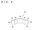
- FIG. 2 is a perspective view of a conductive member 70A provided in the present embodiment.
- FIG. 3 is a cross-sectional view of the conductive member 70A shown in FIG. 2 .
- the photoelectric conversion element 1A of the present embodiment includes a structural body 50 composed of at least a conductive first electrode 10 provided with a porous oxide semiconductor layer 13 supporting a sensitizing dye, a second electrode 20 provided opposite the first electrode 10, and an electrolyte 30 provided in at least part of a space between the first electrode 10 and the second electrode 20, a cover member 60 that covers the structural body 50 and forms a separation portion 80 between the cover member and the second electrode 20, and a conductive member 70A in the separation portion 80, the conductive member having a connection site 70a electrically connected to the second electrode 20.
- the first electrode 10 is a conductive substrate provided with a porous oxide semiconductor layer 13 and is, for example, a transparent electrode composed of a first base material 11, a transparent conductive film 12 provided on one surface 11a of the first base material 11, and the porous oxide semiconductor layer 13 provided on the one surface 11a of the first base material 11, with a transparent conductive film 12 being interposed therebetween.
- a wiring 71 that is used to take the power to the outside of the photoelectric conversion element 1A is electrically connected to the first electrode 10.
- the wiring 71 is not particularly limited and any conventional wiring can be used.
- the wiring 71 is led out to the outside of the photoelectric conversion element 1A via a through hole (not shown in the figure) provided in the cover member 60. In this case, the through hole used to lead out the wiring 71 is sealed with a resin or the like.
- a substrate composed of a light-transmissive material is used as the first base material 11.
- any material that is usually used as a transparent substrate for a solar cell such as glass, polyethylene terephthalate, polyethylene naphthalate, polycarbonate, and polyethersulfones, can be used.
- a material with as excellent light transmissivity as possible is preferred as the first base material 11, and a substrate with a transmissivity of equal to or higher than 85% is even more preferred.
- the porous oxide semiconductor layer 13 is not particularly limited and any material that is usually used to form a porous semiconductor of a photoelectric conversion element can be used.
- suitable semiconductors include TiO 2 , SnO 2 , WO 3 , ZnO, Nb 2 O 5 , In 2 O 3 , ZrO 2 , Y 2 O 3 , and Al 2 O 3 .
- a sensitizing dye is supported on the porous oxide semiconductor layer 13, examples thereof including ruthenium complexes, iron complexes, metal complexes of a porphyrin system or phthalocyanine system and organic dyes such as eosin, rhodamine, merocyanine, and coumarin.
- the sensitizing dye can be appropriately selected for use correspondingly to the application or material of the porous oxide semiconductor layer 13.
- the transparent conductive film 12 is a thin film provided on the one surface 11a of the first base material 11 to impart electric conductivity to the first electrode 10.
- the transparent conductive film 12 is preferably a thin film composed of a conductive metal oxide, so as to obtain a structure in which the transparency of the fist electrode 10 is not significantly degraded.
- Examples of conductive metal oxides forming the transparent conductive film 12 include tin-added indium oxide (ITO), fluorine-added tin oxide (FTO), tin oxide (SnO 2 ), and zinc oxide (ZnO).
- the transparent conductive film 12 has a film composed of the aforementioned conductive oxide.
- the transparent conductive film 12 may be configured of a single layer of such a film or may be configured of a laminated body.
- the transparent conductive film 12 be a single-layer film composed only of FTO or a laminated film obtained by laminating a film composed of FTO on a film composed of ITO.
- the first electrode 10 that excels in chemical resistance and heat resistance, demonstrates small light absorption in a visible range, and has high electric conductivity.
- the second electrode 20 can be configured of a variety of metal substrates with a passive surface, preferably a titanium plate. Further, if necessary, the second electrode 20 can have a catalyst film (not shown in the figure) composed of a metal such as Pt, C, or polyethylene dioxythiophene (PEDOT) on the surface facing the first electrode 10. In this case, it is preferred that the catalyst film be configured of a metal such as Pt.
- the electrolyte 30 is obtained by disposing an electrolytic solution between the first electrode 10 and the second electrode 20 and impregnating the porous oxide semiconductor layer 13 with the electrolytic solution and then gelling (pseudo-solidifying) the electrolytic solution by using an appropriate gelling agent to integrate the electrolyte with the first electrode 10 and the second electrode 20.
- a gelled electrolyte including oxide semiconductor particles or conductive particles can be used.
- An organic solvent including redox species or an ionic liquid can be used as the electrolytic solution.
- An electrolyte obtained by introducing an appropriate gelling agent (a high-molecular gelling agent, a low-molecular gelling agent, various nanoparticles, carbon nanotubes, and the like) into such an electrolytic solution to decrease flowability may be also used.
- the organic solvent is not particularly limited and organic solvents such as acetonitrile, methoxyacetonitrile, propionitrile, propylene carbonate, ethylene carbonate, diethyl carbonate, and ⁇ -butyrolactone can be used.
- Ionic liquids composed of cations having a quaternized nitrogen atom such as imidazolium cations, pyrrolidonium cations, and pyridinium cations and iodide ions, bistrifluoromethane sulfonylimide anions, dicyanoamide anions, and thiocyanic acid anions can be selected as the ionic liquid.
- Redox species are not particularly limited and those formed by adding iodine/iodide ions and bromine/bromide ions can be selected.
- the redox species can be provided by adding a iodide salt (lithium salt, derivatives of quaternary imidazolium salt, and tetraalkylammonium salts can be used individually or in combinations thereof) and iodine individually or in combinations thereof.
- various additives such as 4-tert-butylpyridine, N-methylbenzimidazole, and guanidinium salt derivatives can be added to the electrolytic solution.
- the sealing resin 40 is used to bond together the first electrode 10 and the second electrode 20 disposed opposite each other and to seal the electrolyte 30 between the first electrode 10 and the second electrode 20.
- the sealing resin 40 is not particularly limited, provided it has excellent adhesiveness with respect to the first electrode 10 and the second electrode 20, but an adhesive composed of a thermoplastic resin having a carboxylic acid group in a molecular chain or a UV-curable resin are preferred.
- suitable resins include Himilan (Du Pont-Mitsui Polychemicals Co., Ltd.) and Bynel (Du Pont Co.).
- the structural body 50 is a dye-sensitized solar cell composed at least of the fist electrode 10, the second electrode 20, the electrolyte 30 disposed between the first electrode 10 and the second electrode 20, and the sealing resin 40 that bonds the first electrode 10 and the second electrode 20 together and seals the electrolyte 30.
- the structural body 50 may be a cell or a module.
- the cover member 60 covers the structural body 50 and may cover the entire structural body 50 or may cover the structural body 50 so that the second electrode 20 is covered and the first electrode 10 is exposed.
- the separation portion 80 can be sealed by providing the cover member 60 at the structural body 50, with a gasket (not shown in the figure) being interposed therebetween.
- a gasket not shown in the figure
- By providing the cover member 60 it is possible to prevent moisture or the like from penetrating into the structural body 50.
- the cover member 60 covers the entire structural body 50, at least a portion of the cover member on the first electrode 10 side has light transmissivity.
- a resin, glass, or a metal plate can be used as the cover member 60, and the cover member 60 can be appropriately selected for use correspondingly to the shape required to cover the structural body 50.
- the structural body 50 When the structural body 50 is covered so that the first electrode 10 is exposed, for example, aluminum, which is a lightweight metal that is easy to process and excels in corrosion resistance, can be used as a material constituting the cover member 60.
- a resin When a resin is used as the cover member 60, the resin can be provided with a gas barrier film (not shown in the figure) such as a vapor-deposited aluminum film, alumina film, silica film, and polyvinyl alcohol film to increase sealing ability.
- a gas barrier film such as a vapor-deposited aluminum film, alumina film, silica film, and polyvinyl alcohol film to increase sealing ability.
- the conductive member 70A is located in the separation portion 80.
- a connection site 70a of the conductive member 70A forms the contact portion ⁇ 1 together with the second electrode 20, and is electrically connected thereto.
- the conductive member 70A is preferably provided to be electrically connected to a central portion of one surface 20c of the second electrode 20. As a result, an electric current can be collected from the center of the one surface 20c of the second electrode 20 that has a high current collection efficiency.
- a material with good electric conductivity is preferably used to constitute the conductive member 70A.
- a material with good electric conductivity include copper or an alloy including copper.
- beryllium copper having a high tensile strength and elasticity and excelling in strength and electric conductivity can be used as the alloy including copper.
- the conductive member 70A is sandwiched by the cover member 60 and the second electrode 20.
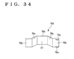
- the conductive member 70A has a flat top surface 70d, inclined first surfaces 70c, and second surfaces 70b parallel to the top surface.
- the top surface 70d is a plate-like cover member contact portion that will be in contact with the cover member 60.
- the second surfaces 70b are plate-like end portions parallel to the cover member contact portion.
- the first surfaces 70c are plate-like connection portions that connect the cover member contact portion with the end portions.
- the first surfaces 70c are inclined with respect to the cover member contact portion and end portions.
- surfaces 70a of the second surfaces 70b which are connection sites facing the second electrode 20, form contact portions ⁇ 1 that are electrically connected to and in a surface contact with the second electrode 20.
- the contact portions ⁇ 1 of the conductive member 70A and the second electrode 20 can be displaced, conduction defects can occur, and current collection efficiency can be decreased.
- the contact force of the conductive member 70A with the second electrode 20 is strong, the second electrode 20 can be damaged. For this reason, it is preferred that the conductive member 70A could be elastically deformed and be disposed in a state of compression by the cover member 60 and the second electrode 20.
- the conductive member 70A can be mechanically brought into contact with the second electrode 20 by an appropriate pressurizing force. Therefore, current collection from the second electrode 20 can be performed with good stability, without damaging the second electrode 20. In addition, even when the distance between the cover member 60 and the second electrode 20 changes due to variations in the external air temperature, the conductive member 70A can deform to accommodate this change. Therefore, conduction between the cover member 60 and the second electrode 20 can be ensured at all times and insufficient conduction caused by changes in air temperature can be prevented.
- the elastic constant of the conductive member 70A is usually 2-50 N/mm, preferably 5-20 N/mm.
- the top surface 70d of the conductive member 70A is a site that will be in contact with the cover member 60 and may be fixed to the cover member 60, for example, with a two-side adhesive tape.
- the first surfaces 70c and the second surfaces 70b can provide for elasticity matching the size of the separation portion 80 or the structural body 50 that will be used, by appropriately adjusting the shape of the first and second surfaces by changing the inclination angle, length, thickness, or width thereof.
- the elasticity of the conductive member 70 can be appropriately adjusted by providing the first surface 70c with necking portions.
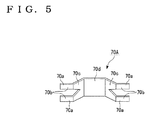
- one second surface 70b is provided with respect to one first surface 70c, but such a shape of the conductive member 70A is not limiting and, for example, as shown in FIG. 5 , the first surfaces 70c can be branched from the intermediate portion thereof and a plurality of second surfaces 70b may be provided with respect to one first surface 70c in the conductive member 70A. With such a configuration, even if an obstacle appears in one surface 70a, which is in contact with the second electrode 20 in the conductive member 70A, the other surface 70a serves as a backup.
- Part of the conductive member 70A may be elastically deformed as in the present embodiment, or for example, as shown in FIG. 6 , the conductive member 70A having a curved shape, that is, the arch-shaped the conductive member 70A can be used and thus the entire conductive member 70 can be elastically deformed.
- Power collected by the conductive member 70 can be taken to the outside of the photoelectric conversion element 1 by a well-known conventional method.
- the power can be taken to the outside of the photoelectric conversion element 1 by connecting a wiring 77 to the conductive member 70 by soldering or the like and leading the wiring 77 to the outside via a through hole (not shown in the figure) provided in the cover member 60.
- the wiring 77 is not particularly limited and a well-known conventional wiring can be used.
- the through hole used when leading the wiring 77 to the outside of the photoelectric conversion element 1 is sealed with a resin or the like.
- the separation portion 80 is a space formed between the second electrode 20 and the cover member 60 and is preferably in a sealed and dried state. As a result, good electric connection of the conductive member 70A and the second electrode 20 can be maintained. In particular, where a dew point of the separation portion 80 is equal to or less than -40°C, condensation is prevented even at a low-temperature guaranteed limit of the photoelectric conversion element 1A and the photoelectric conversion element 1A with excellent resistance to environment can be obtained.
- the conductive member 70A is sandwiched between the cover member 60 and the second electrode 20. Therefore, the conductive member 70A is fixed, without soldering, in a predetermined position on the second electrode 20. Further, the conductive member 70A is electrically connected by contact to the second electrode 20. For this reason, when the electricity generated by the structural body 50 is taken out, the current can be conveniently collected from the conductive member 70A.
- the second electrode 20 and structural body 50 in particular, the porous oxide semiconductor layer 13
- the photoelectric conversion element 1A current collection can be conveniently performed without degrading the photoelectric conversion characteristic.
- FIG. 7 is a cross-sectional view showing schematically a photoelectric conversion element 1B of the second embodiment of the present invention.
- components similar to those of the photoelectric conversion element 1A of the first embodiment are assigned with same reference numerals and explanation thereof is herein omitted.
- the photoelectric conversion element 1B according to the second embodiment differs from the photoelectric conversion element 1A of the first embodiment in that a wiring 90 is disposed on the first electrode 10, a conductive member 70B is further provided, and the conductive member 70B is electrically connected to the first electrode 10 via the wiring 90.
- a wiring 77 that takes out the power collected in the same manner as in the first embodiment to the outside of the photoelectric conversion element 1 is electrically connected to the conductive member 70B.
- the wiring 90 is a current-collecting wiring provided so as to surround the porous oxide semiconductor layer 13 on the surface of the first electrode 10 and is electrically connected to the first electrode 10.
- the wiring 90 can be formed, for example, from silver, gold, platinum, aluminum, nickel, and titanium.
- the width of the wiring is preferably 300 ⁇ m to 1 cm in order to prevent light transmissivity of the first electrode 10 from being significantly decreased. It is even more preferred that the wiring width be as small as 500 ⁇ m or less.
- the thickness of the wiring 90 is for example, 0.1-50 ⁇ m. Any material causing passivation cannot be necessarily used to form the wiring 90.
- a protective layer 91 composed for example of glass with a low melting point be provided on the surface of the wiring 90 to protect the wiring 90 from corrosion induced by the electrolytic solution.
- the conductive member 70B is in contact with the wiring 90 formed on the first electrode 10, forms a contact portion ⁇ 2, and is electrically connected to the first electrode 10.
- the surface area of the wiring 90 (or the first electrode 10) that is exposed to the separation portion 80 is much smaller than the surface area of the second electrode 20. Therefore, only one end of the conductive member 70B is in contact with the wiring 90 (or the first electrode 10) and the other end is in contact with an insulating film 22 provided on the second electrode 20, as shown in FIG. 7 , by contrast with the configuration according to the first embodiment in which both ends of the conductive member 70B are in contact with the second electrode 20.
- the other end of the conductive member 70B is disposed so as to be separated from the second electrode 20 by the insulating film 22. Further, the conductive member 70B has a shape such that one second surface 70b from among the two second surfaces 70b in the conductive member 70A is perpendicular to the top surface 70d.
- the conductive member 70B be elastically deformable and disposed in a state of compression by the cover member 60 and the first electrode 10, similarly to the conductive member 70A.
- the material of the insulating film 22 is not particularly limited and, for example, PET, PEN, and paper can be used.
- the thickness of the insulating film is preferably 25 ⁇ m to 200 ⁇ m.
- the conductive member 70B is sandwiched by the cover member 60 and the first electrode 10, and both ends of the conductive member are fixed to the second electrode 20 and the first electrode 10, respectively. Further, the conductive member 70B is electrically connected by the wiring 90 to the first electrode 10. Therefore, when electric current is collected from the first electrode 10, since it is not necessary to connect the wiring or the like to the first electrode 10 by soldering, current collection can be performed without damaging the first electrode 10 or the structural body 50 by the heat generated by soldering. Further, since the conductive member 70B is electrically connected by contact to the first electrode 10, current collection can be conveniently performed from the first electrode 10. In addition, when the cover member 60 is provided and the separation portion 80 is maintained in a sealed and dried state, good electric connection of the conductive member 70B and the first electrode 10 can be obtained.
- the conductive member 70A is used separately, as shown in FIG. 7 , to collect current from the second electrode 20 in the same manner as in the first embodiment.
- the yield can be increased without damaging the first electrode 10, the second electrode 20, and the structural body 50 and the current can be conveniently collected from the first electrode 10 and the second electrode 20.
- the first electrode 10 and the conductive member 70B are electrically connected by the wiring 90, but the first electrode 10 and the conductive member 70B can be also electrically connected directly, that is, without the wiring 90.
- FIG. 8 is a cross-sectional view of a photoelectric conversion element 1C of the present embodiment.
- FIG. 9 is a perspective view of a conductive member 170A provided in the photoelectric conversion element 1C shown in FIG. 8 .
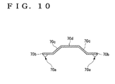
- FIG. 10 is a cross-sectional view of the conductive member 170A shown in FIG. 9 .
- components similar to those of the photoelectric conversion elements of the first and second embodiments are assigned with same reference numerals and explanation thereof is herein omitted.
- the photoelectric conversion element 1C of the third embodiment differs from the photoelectric conversion element 1A of the first embodiment in that connection sites 70a by which the conductive member 170A is electrically connected to the second electrode 20 have a protruding shape and a contact portion ⁇ 1 with the second electrode 20 forms a point contact.
- connection sites 70a at the second surfaces 70b that are in contact with the second electrode 20 have a protruding shape.
- the connection sites 70a bite into the second electrode 20 and are strongly fixed thereto.
- the conductive member 170A can readily break through the passivation layer and come into contact with the second electrode 20.
- this passivation layer can be broken through even easier and contact with the second electrode 20 can be attained even easier.
- the surface of the second electrode 20 be plastically deformed by applying pressure to the contact portion.
- the connection site 70a of the conductive member 170A sinks to a depth of equal to or greater than 250 nm from the average surface of the second electrode 20.
- the passivation layer that has been formed on the second electrode 20 is crushed through to connect electrically the conductive member 170A and the second electrode 20 and therefore the electric resistance can be reduced. Further, due to point contact, a sufficient pressurizing force can be obtained.
- the passivation layer formed on the surface of the second electrode 20 can be broken through by just applying a pressure to the contact portion ⁇ 1 of the conductive member 170A and the second electrode 20 via the cover member 60, good electric connection, that is, decreased electric resistance, can be conveniently attained without conducting surface treatment of the second electrode 20 and conductive member 170A.
- connection site 70a can be conveniently formed in a desired convex shape by machining with a laser or the like.
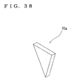
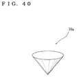
- the connection site 70a has a triangular plate shape as shown in FIG. 38 , but it may also have a tetragonal pyramidal shape (see FIG. 39 ) and a conical shape (see FIG. 40 ).
- the conductive member 170A used in the present embodiment also can be a conductive member provided with a necking portion in the first surface 70c, a conductive member in which the first surface 70c is divided in the intermediate section and a plurality of second surfaces 70b are provided with respect to one first surface 70c, and a conductive member composed of a curved surface.
- FIG. 11 is a perspective view illustrating an example of the conductive member 170A provided with a necking portion in the first surface 70c.
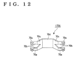
- FIG. 12 is a perspective view illustrating an example of the conductive member provided with a plurality of second surfaces 70b with respect to one first surface 70c. As shown in FIG.
- FIG. 13 is a side view illustrating schematically another example of the conductive member 170A. As shown in FIG. 13 , by using the conductive member 70 with a curved surface, that is, the conductive member 70 of an arch-like shape, it is possible to ensure the efficient transfer of force when the conductive member 170A is pressurized and break through the passivation layer reliably.
- the wiring 90 can be provided at the first electrode 10 and a state can be obtained in which the conductive member 170B is electrically connected to the first electrode 10 via the wiring 90.
- the connection site 70a of the conductive member 170B that is in contact with the insulating film 22 do not have a protruding shape. In this case, the connection site 70a can be prevented from passing through the insulating film 22 and electrically connecting to the second electrode 20.
- the conductive members 170A, 170B be elastically deformable similarly to the conductive member 70A and be disposed in a state of compression by the cover member 60 and the first electrode 10.
- the elastic constants of the conductive members 170A, 170B are also similar to that of the conductive member 70A.
- FIGS. 15 to 17 are cross-sectional views illustrating schematically the photoelectric conversion elements (1D-1F) of the fourth to sixth embodiments.
- components similar to those of the photoelectric conversion elements (1A-1C) of the first to third embodiments are assigned with same reference numerals and explanation thereof is herein omitted.
- the photoelectric conversion elements (1D-1F) of the fourth to sixth embodiments differ from the photoelectric conversion elements (1A-1C) of the first to third embodiments in that a drying means 81 is provided in the separation portion 80.
- the photoelectric conversion element 1D of the fourth embodiment shown in FIG. 15 is obtained by providing the drying means 81 in the separation portion 80 of the photoelectric conversion element 1A of the first embodiment.
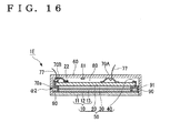
- the photoelectric conversion element 1E of the fifth embodiment shown in FIG. 16 is obtained by providing the drying means 81 in the separation portion 80 of the photoelectric conversion element 1B of the second embodiment.
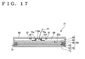
- the photoelectric conversion element 1F of the sixth embodiment shown in FIG. 17 is obtained by providing the drying means 81 in the separation portion 80 of the photoelectric conversion element 1C of the third embodiment.
- a drying agent such as silica gel or molecular sieves can be used as the drying means 81.
- the drying means 81 is provided in the separation portion 80, even if moisture penetrates into the separation portion 80, the drying means 81 can absorb the moisture maintain the separation portion 80 in a dried state. Therefore, the dry state of the separation portion 80 can be maintained with good stability for a long time and good electric connection between the second electrode 20 and the conductive members 70A, 170A or between the first electrode 10 and the conductive member 70B can be maintained. Therefore, photoelectric conversion elements (1D-1F) with excellent resistance to environment can be obtained.
- the photoelectric conversion element 1F of the sixth embodiment that is obtained by providing the photoelectric conversion element 1C of the third embodiment with the drying means 81, by providing the drying means 81 in the separation portion 80, it is possible to prevent a passivation layer from being formed again in the contact portion ⁇ 1 and to suppress the increase in electric resistance even after the contact portion ⁇ 1 has been formed by the conductive member 170B piercing through the passivation layer formed on the second electrode 20.
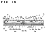
- FIG. 18 is a cross-sectional view illustrating schematically a photoelectric conversion element 1G according to the seventh embodiment.
- components similar to those of the photoelectric conversion elements of the first to sixth embodiments are assigned with same reference numerals and explanation thereof is herein omitted.
- the photoelectric conversion element 1G of the seventh embodiment includes a structural body 50A and a structural body 50a.
- the structural body 50A is composed of at least a conductive first electrode 10A provided with a porous oxide semiconductor layer 13 supporting a sensitizing dye, a second electrode 20A provided opposite the first electrode 10A, and an electrolyte 30A provided in at least part of a space between the first electrode 10A and the second electrode 20A.
- the structural body 50a is composed of at least a conductive first electrode 10a provided with a porous oxide semiconductor layer 13 supporting a sensitizing dye, a second electrode 20a provided opposite the first electrode 10a, and an electrolyte 30a provided in at least part of a space between the first electrode 10a and the second electrode 20a.
- the photoelectric conversion element 1G further includes a conductive member 70C that electrically connects the second electrode 20A of one structural body 50A and the first electrode 10a of the other structural body 50a.
- material that causes passivation cannot be necessarily used to constitute the wiring 90.
- the first base material 11 may be a module in which a plurality (four in the example shown in the figure) of cell units C having formed therein a power-generating layer composed of the transparent conductive film 12 and the porous oxide semiconductor layer 13 are two-dimensionally arranged on the one surface 11a of the first base material.
- connection site 70a of the conductive member 70C that is in contact with the second electrode 20A preferably has a protruding shape.
- the conductive member 70C is fixed to the cover member 60.
- the conductive member 70C is sandwiched between the cover member 60 and the first electrode 10a and also between the cover member 60 and the second electrode 20A.
- the second electrode 20A of the one structural body 50A and the wiring 90a of the other structural body 50a can be brought into contact with good positional accuracy and the reliability of electric connection can be increased.
- the structural bodies 50A, 50a can be conveniently ensured by electrically connecting the one structural body 50A with the other structural body 50a by using the conductive member 70C.
- the conductive member 70C is sandwiched between the cover member 60 and the first electrode 10a and also between the cover member 60 and the second electrode 20A.
- the structural body 50 namely, the wiring 90, the second electrode 20 or the like, can be prevented from damage caused by the heat generated during soldering, and the photoelectric conversion characteristic can be prevented from being degraded.
- the present invention is not limited to this configuration and three or more structural bodies may be used so that the adjacent structural bodies are electrically connected by using the conductive members 70C.
- the conductive member 170A or 170B in the same manner as in the first to third embodiments of the present invention when current collection is performed from the first electrode 10 and the second electrode 20, it is possible to collect current conveniently from the first electrode 10 and the second electrode 20.
- the conductive member 170A such as used in the third embodiment, it is possible to ensure electric conduction by breaking through the passivation layer formed on the second electrode 20 and therefore the electric resistance can be reduced.
- the drying means 81 can be provided in the separation portion 80. Where the drying means 81 is provided, even if moisture penetrates into the separation portion 80, the drying means 81 can absorb the moisture and maintain the separation portion 80 in a dried state. Therefore, the dry state of the separation portion 80 can be maintained with good stability for a long time and good electric connection between the second electrode 20 and the conductive members 170A, 70C or between the first electrode 10 and the conductive members 170B, 70C can be maintained. Therefore, the photoelectric conversion element 1G with excellent resistance to environment can be obtained.
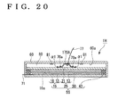
- FIG. 20 is a cross-sectional view illustrating schematically a photoelectric conversion element 1H according to the eighth embodiment.
- components similar to those of the photoelectric conversion element 1A of the first embodiment are assigned with same reference numerals and explanation thereof is herein omitted.
- the photoelectric conversion element 1H of the present embodiment is essentially constituted by a structural body 55 composed of at least a third electrode 25 composed of an electrically conductive member provided with a porous oxide semiconductor layer 13 supporting a photosensitive dye, a conductive fourth electrode 15, and an electrolyte 30 provided in at least part of a space between the third electrode 25 and the fourth electrode 15. Further, the photoelectric conversion element 1H also has a cover member 60 that covers the structural body 55 so that a separation portion 80 is provided between the third electrode 25 and the cover member and the fourth electrode 15 is exposed and at least one conductive member 170A provided at a surface 60a of the cover member 60 that faces the third electrode 25. The conductive member 170A is electrically connected by contact to the third electrode 25.
- the structural body 55 and the cover member 60 may have flexibility.
- a resin is used as the cover member 60, and sealing ability can be increased by providing a gas barrier film (not shown in the figure).
- a gas barrier film not shown in the figure.
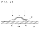
- the cover member 60 be caused to apply a pressure to the conductive member 170A by pushing from the outside or reducing the internal pressure, as shown in FIG. 41 , to ensure a pressurizing force of the conductive member 170A.
- the porous oxide semiconductor layer 13 is formed on a conductive metal substrate 21.
- the metal substrate 21 is similar to the metal substrate 21 forming the second electrode 20 in the first embodiment.
- the porous oxide semiconductor layer 13 is similar to the porous oxide semiconductor layer 13 constituting the first electrode 10 of the first embodiment.
- the fourth electrode 15 is a transparent electrode composed of a conductive substrate, for example, a fourth base material 16 and a transparent conductive film 12 provided on one surface 16a of the fourth base material 16.
- the fourth base material 16 and the transparent conductive film 12 are respectively similar to the first base material 11 and the transparent conductive film 12 forming the first electrode 10 of the first embodiment.
- the electrolyte 30, sealing resin 40, and cover member 60 are similar to those of the first embodiment.
- the conductive member 170A may be the conductive member 70A of the first embodiment.
- the conductive member 170A is also sandwiched between the cover member 60 and the third electrode 25 and electrically connected to the third electrode 25 of the structural body 55.
- current collection can be conveniently performed from the third electrode 25. Since no soldering or the like is required, the structural body 55 can be prevented from damage induced by the heat generated during soldering, and the degradation of the photoelectric conversion characteristic can be prevented.
- the contact portion ⁇ 1 of the conductive member 170A and the third electrode 25 is brought into contact by causing plastic deformation and contact thereof is ensured by piercing the passivation layer formed on the third electrode 25. Therefore, the electric resistance can be decreased.
- FIG. 21 is a cross-sectional view illustrating schematically a photoelectric conversion element 201A according to the ninth embodiment of the present invention.
- components similar to those of the photoelectric conversion elements of the first to eighth embodiments are assigned with same reference numerals and explanation thereof is herein omitted.
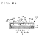
- the photoelectric conversion element 201A shown in FIG. 21 represents an example in which wiring portions 85A, 85B are wiring portions formed, for example, by a printing method, and the locations where the wiring portions 85A, 85B are provided are on the inner surface of the cover member 60.
- the photoelectric conversion element 201A of the ninth embodiment is essentially constituted by a structural body 50 composed of at least a conductive first electrode 10 provided with a porous oxide semiconductor layer 13 supporting a photosensitive dye, a second electrode 20 diposed opposite the first electrode 10, an electrolyte 30 provided in at least part of a space between the first electrode 10 and the second electrode 20, and sealing resins 40, 91 bonding together the first electrode 10 and the second electrode 20 and sealing the electrolyte 30, a cover member 60 that covers the structural body 50 and forms a separation portion 80 between the cover member and the second electrode 20, and wiring 90 provided so as to surround the porous oxide semiconductor layer 13 on the surface of the first electrode 10.
- the wiring portion 85A for ensuring electric connection with the second electrode 20 is provided on the inner surface of the cover member 60 on the separation portion 80 side.
- the photoelectric conversion element 201A also has a conductive member 270A that is pressurized by and brought into contact with the second electrode 20 and the wiring portion 85A, and a conductive member 270B which electrically connects the wiring portion 85B to the first electrode 10.
- the conductive member 270A is disposed in a path for taking out the output from the second electrode 20, and the conductive member 270B is disposed in the path for taking out the output from the first electrode 10.
- the wiring portions 85A, 85B are provided on the inner surface of the cover member 60 on the separation portion 80 side. In the present embodiment, these portions are printed wiring portions formed on the inner surface of the cover member 60.
- the wiring portions 85A, 85B are formed by print coating an electrically conductive paste on the inner surface of the cover member 60 by a printing method such as a screen printing method.
- a conductive member similar to the conductive member 170A of the fourth embodiment, but additionally having a convex second connection site 70e on top surface 70d on the cover member 60 side is used as the conductive member 270A.
- parts of the wiring portion 85A and the second electrode 20 are plastically deformed by pressurization-induced contact.
- the contact portions ⁇ 1 and ⁇ 2 of the conductive member 270A penetrate to a depth of equal to or greater than 250 nm from the average surface of the second electrode 20 and the wiring portion 85A.
- the conductive member 270A pierces the passivation layer formed on the second electrode 20 and is electrically connected to the second electrode 20 and the wiring portion 85A. Therefore, the electric resistance can be reduced.
- a conductive member similar to the conductive member 170B or the conductive member 70B, but additionally having a concave second connection site 70e on the top surface 70d on the cover member 60 side can be used as the cover member 270B.
- the conductive member 270A is preferably provided so as to be electrically connected to the central portion of the one surface 20c of the second electrode 20. As a result, current collection can be performed with high efficiency from the center of the one surface 20c of the second electrode 20. Further, it is preferred that a plurality of sites 70a (first connection sites) which are the sites of the conductive member 270A that are in contact with the second electrode 20 and a plurality of sites 70e (second connection sites) which are the cites of the conductive member that are in contact with the wiring portion 85 be provided. With such a configuration, even if an obstacle appears in one of the first connection sites 70a, other first connection sites serve as a backup.
- the cover member 60 is provided so that the separation portion 80 is provided between the cover member and the second electrode 20 in order to obtain a dry state of the contact portions ⁇ 1 and ⁇ 2 of the conductive members 270A, 270B and the first electrode 10, second electrode 20, and wirings 85A, 85B.
- the cover member 60 covers the structural body 50 and may cover the entire structural body 50 or may cover the structural body 50 so that the second electrode 20 is covered and the first electrode 10 is exposed.
- cover member 60 when the cover member 60 covers the entire structural body 50, at least a portion of the cover member on the first electrode 10 side has light transmissivity.
- a resin, glass, or a metal plate can be used as the cover member 60, and the cover member 60 can be appropriately selected for use correspondingly to the shape required to cover the structural body 50.
- the structural body 50 is covered so that the first electrode 10 is exposed, for example, aluminum, which is a lightweight metal that is easy to process and excels in corrosion resistance, can be used as a material constituting the cover member 60.
- the resin When a resin is used as the cover member 60, the resin can be provided with a gas barrier film (not shown in the figure) such as a vapor-deposited aluminum film, alumina film, silica film, and polyvinyl alcohol film to increase sealing ability.
- a gas barrier film such as a vapor-deposited aluminum film, alumina film, silica film, and polyvinyl alcohol film to increase sealing ability.
- the wiring portions 85A, 85B are formed on the inner surface of the cover member 60, but in this case, for example, an insulating film is formed over the entire surface of the cover member 60 serving as a region at least for carrying the wiring portions 85A, 85B on the inner surface and outer surface of the cover member 60, and the wiring portions 85A, 85B are formed on the insulating film. This is done to prevent the wiring portions 85A, 85B and the first electrode 10 from short circuiting.
- Through holes 87A, 87B through which the separation portion 80 communicates with the outside are formed in the cover member 60.
- Through connectors 86A, 86B are inserted, in a state of insulation from the cover member 60, into the through holes 87A, 87B.
- One end side of the through connectors 86A, 86B (first terminals) exposed inside the separation portion 80 is electrically connected to the wiring portion 85 provided on the inner surface side of the cover member 60, and the other end side is exposed to the outside.
- current collection from the first electrode 10 and the second electrode 20 is performed via the conductive members 270A, 270B, wiring portions 85B, 85A, and through connectors 86A, 86B.
- the conductive member 270B is electrically connected by contact to the wiring 90 formed at the first electrode 10. Since the surface area of the wiring 90 exposed to the separation portion 80 is much smaller than the surface area of the second electrode 20, the two ends are not in contact, as in the conductive member 270A, only one end of the conductive member 270B is in contact with the wiring 90, and the other end is in contact with the insulating film 22 provided on the second electrode 20. In order to prevent the first connection site 70a of the conductive member that is in contact with the insulating film 22 from passing through the insulating film 22 and being electrically connected to the second electrode 20, it is preferred that the first connection site 70a do not have a convex shape.
- the conductive member 270A is sandwiched between the cover member 60 and the second electrode 20. Therefore, the conductive member 270A is fixed, without soldering, in a predetermined position on the second electrode 20. Further, the conductive member 270A is electrically connected by contact to the second electrode 20 and the wiring portion 85A, and the second electrode 20 and the through connector 86A are electrically connected to each other.
- the conductive member 270B is sandwiched between the cover member 60 and the first electrode 10. Therefore, the conductive member 270B is fixed, without soldering, in a predetermined position on the first electrode 10. Further, the conductive member 270B is electrically connected by contact to the first electrode 10 and the wiring portion 85B, and the first electrode 10 and the through connector 86B are electrically connected to each other.
- the first electrode 10, the second electrode 20, or the structural body 50 in particular, the porous oxide semiconductor layer 13
- current collection can be conveniently performed without degrading the photoelectric conversion characteristic.
- the first connection site 70a by which the conductive member 270A comes into contact with the second electrode 20 has a convex (protruding) shape. Therefore, the first connection site 70a can bite into the second electrode 20, and the conductive member 270A can be more strongly fixed to the second electrode 20. Even in the case in which a passivation layer such as an oxide film has formed on the one surface 20c of the second electrode 20, this passivation layer can be easily broken through and contact with the second electrode 20 and the wiring portion 85A can be easily attained.
- the first connection site 70a has a sharp convex shape
- this passivation layer can be broken through even easier and contact with the second electrode 20 and the wiring portion 85A can be attained even easier.
- a sufficient pressurizing force acting upon the wiring portion 85A and the second electrode 20 and connection reliability can be improved.
- the passivation layer formed on the second electrode 20 can be broken through by just pressurizing the contact portions ⁇ 1, ⁇ 2 of the conductive member 270A with the second electrode 20 and the wiring portion 85A via the cover member 60. Therefore, good electric connection, that is, reduction in electric resistance, can be ensured without performing surface treatment of the second electrode 20 and wiring portions 85A or the conductive member 270A. It is preferred that the protruding shape of the conductive member 270A be appropriately adjusted correspondingly to the distance of the separation portion 80 between the structural body 50 and the cover member 60 so as to prevent the application of an excess pressure to the contact portion. In this case, current collection can be performed without damaging the structural body 50.
- the first connection site 70a and the second connection site 70e can be conveniently formed in a desired convex shape by machining with a laser or the like.
- the second connection site 70e of the conductive member 270A is in contact with the wiring portion 85A and made convex.
- the second connection site 70e can be caused to bite into the wiring portion 85A, and the conductive member 270A can be fixed stronger to the wiring portion 85A. Therefore, sufficient conduction between the wiring portion 85A and the conductive member 270A can be ensured and the occurrence of poor conduction can be sufficiently prevented.
- the wiring portion 85A at the cover member 60 it is possible to ensure the conduction to the outside more conveniently than in the case in which the wiring portion 85A is not provided.
- the photoelectric conversion element 201A also has the following advantages.
- the conductive member 270A is provided, the conductive member 270A is positioned between the second electrode 20 and the wiring portion 85A provided on the inner surface of the cover member 60, and the distance between the cover member 60 with the wiring portion 85A and the second electrode 20 is reduced by pushing the cover member 60.
- the convex second connection site 70e of the conductive member 270A bites into the wiring portion 85A and is supported in the fixed position.
- convex first connection site 70a moves along the second electrode 20, the second connection site 70e serving as a pivot point.
- the passivation layer of the upper surface of the second electrode 20 along which the second connection site 70e moves undergoes plastic deformation and is broken through, whereby reliable electric connection of the first connection site 70a and the second electrode 20 is ensured.
- the conductive member 270A efficiently pierces through the passivation layer formed on the second electrode 20 and conduction is established by just applying an appropriate pressure to the cover member 60 when the cover member 60 is mounted. Therefore, the electric resistance can be conveniently reduced.
- FIG. 22 is a perspective view illustrating schematically the conductive member 270A for use in the photoelectric conversion element according to the ninth embodiment of the present invention.
- FIG. 23 is a cross-sectional view illustrating the conductive member shown in FIG. 22 .
- the conductive member 270A is composed of a flat top surface 70d, inclined first surfaces 70c, second surfaces 70b parallel to the top surface 70d, convex connection sites (first connection sites) 70a formed at the second surface 70b, and a convex connection site (second connection site) 70e formed at the top surface 70d.
- the second connection site 70e provided at the top surface 70d of the conductive member 270A will come into contact with the wiring portion 85A provided on the lower surface of the cover member 60, and the first connection site 70a provided at the second surface 70b will come into contact with the fist electrode 10 or the second electrode 20.
- the first surfaces 70c and the second surfaces 70b can be provided with elasticity matching the size of the separation portion 80 or the structural body 50 that will be used, by appropriately adjusting the shape of the first and second surfaces by changing the inclination angle, length, thickness, or width thereof or by providing a necking portion.
- one second surface 70b is provided with respect to one first surface 70c, but such a shape of conductive member 270A is not limiting and, for example, the first surfaces 70c can be branched off from the intermediate portion thereof and a plurality of second surfaces 70b may be provided with respect to one first surface 70c.
- the conductive member 270A be formed from an elastically deformable material. In such a case, an appropriate pressurizing force can be maintained. When the pressurizing force is insufficient, the passivation layer of the second electrode 20 can grow again. Further, when the pressurizing force is too strong, the conductive member 270A can pierce the second electrode 20 and the wiring portion 85A and the first electrode 10 can be crushed via the second electrode 20.
- an elastically deformable conductive member 270A in contact with the second electrode 20 of the structural body 50 and the wiring portion 85A, it is possible to inhibit the damage of the second electrode 20, structural body 50, and wiring portion 85A, increase the yield, and prevent the passivation layer from growing again and increasing the resistance value.
- the conductive member 270A is preferably fixed in a state of compression between the cover member 60 and the wiring portion 85A. In this case, mechanical contact with the second electrode 10 can be ensured by an appropriate pressurizing force. In addition, even when the distance between the cover member 60 and the second electrode 20 changes due to variations in the external air temperature, the conductive member 270A can deform to accommodate this change. Therefore, conduction between the cover member 60 and the second electrode 20 can be ensured at all times and insufficient conduction caused by changes in air temperature can be prevented.
- the elastic constant of the conductive members 270A, 270B is similar to that of the conductive member 70A.
- a drying agent can be provided as a drying means 81 in at least part of the separation portion 80.
- the drying agent can absorb the moisture and maintain the separation portion 80 in a dried state.
- the penetration of moisture into the structural body 50 and formation of the passivation layer again on the second electrode 20 can be inhibited more effectively. Therefore, good electric connection of the second electrode 20 to the wiring portion 85A and the conductive member 270A can be maintained and the initial resistance value can be maintained over a long period. Therefore, a photoelectric conversion element with excellent resistance to environment can be obtained.
- FIG. 24 is a cross-sectional view illustrating schematically a photoelectric conversion element 201B according to the tenth embodiment.
- components similar to those of the photoelectric conversion elements of the ninth embodiment are assigned with same reference numerals and explanation thereof is herein omitted.
- a gasket GT is used to join the first base material 11 and the cover member 60.
- the gasket GT performs sealing at the outer circumferential end ED of the first base material 11, while providing the separation portion 80 between the first electrode 10 and the cover member 60 so as to incorporate the second electrode 20 therein.
- gasket GT is used for sealing at the outer circumferential end ED of the first base material 11, while providing the separation portion 80 between the first electrode 10 and the cover member 60 so as to incorporate the second electrode 20 constituting the structural body 50 therein.
- the cover member 60 By so covering the second electrode 20 in a dry state by the cover member 60, it is possible to maintain the separation portion 80 in a dried state. Therefore, the formation of a passivation layer on the one surface 20c of the second electrode 20 can be inhibited. Further, the penetration of moisture or the like into the structural body 50 can be inhibited.
- the aforementioned drying means 81 is preferably provided in the separation portion 80 to maintain the dry state.
- FIG. 25 is a view illustrating schematically a photoelectric conversion element 201C according to the eleventh embodiment.
- components similar to those of the photoelectric conversion elements of the ninth and tenth embodiments are assigned with same reference numerals and explanation thereof is herein omitted.
- the photoelectric conversion element 201C shown in FIG. 25 is an example of the photoelectric conversion element in which wiring portions 85A, 85B are printed wirings composed for example of silver, the locations where the wiring portions 85A, 85B are provided are on the inner surface of the cover member 60, and the wiring portions 85A, 85B are taken out from the flanks 85a of the cover member.
- the wiring portions 85A, 85B are printed wiring portions formed from the inner surface to the outer surface of the cover member 60 in the region from the separation portion 80 side to the outer surface.
- an insulating film is formed on the surface of the cover member 60 and the printed wirings are formed on the insulating film.
- the wiring portions 85A, 85B are formed by coating an electrically conductive paste on a region from the inner surface to the outer surface of the cover member 60 by a printing method such as screen printing.
- Connectors 88A, 88B (second terminal) are fixed to the cover member 60, and the connectors 88A, 88B and the printed wiring portions 85A, 85B are electrically connected.
- current collection can be also conveniently performed from the first electrode 10 and the second electrode 20 at the connectors 88A, 88B via the conductive members 270A, 270B and the printed wiring portions 85A, 85B.
- the wiring portions 85A, 85B are constituted by printed wiring portions, but conductor portions of a flexible printed circuit board (first flexible printed circuit board) may be also used instead of the printed wiring portions.
- the required configuration can be obtained by pasting the flexible printed circuit board on the inner surface and outer surface of the cover member 60 with an adhesive or the like.
- the gasket GT is used in the same manner as in the photoelectric conversion element 201B according to the tenth embodiment.
- the gasket GT seals the outer circumferential ends ED of the first electrode 10 and the cover member 60, while providing the separation portion 80 therebetween, so that the second electrode 20 is inside the separation portion.
- FIG. 26 is a cross-sectional view illustrating schematically a photoelectric conversion element 201D according to the twelfth embodiment.
- components similar to those of the photoelectric conversion elements of the ninth and tenth embodiments are assigned with same reference numerals and explanation thereof is herein omitted.
- the wiring portions are etching wirings formed for example from copper, and the wiring portions are provided on a flexible printed circuit board 89 having gas barrier properties.
- the flexible printed circuit board 89 is connected to an external take-out location via lead wires 102a, 102b (see FIG. 28 and FIG. 29 ).
- the external take-out location is a through connector 101 provided in a through hole 100 of the cover member 60.
- the flexible printed circuit board 89 (the second flexible printed circuit board) is provided inside the separation portion 80 formed between the structural body 50 and the cover member 60, so as to cover the conductive members 270A, 270B and also to position the conductive members 270A, 270B and seal the space between the flexible printed circuit board and the structural body 50.
- the wiring portion 85 is a conductor 92 of the flexible printed circuit board 89.
- the through hole 100 through which the separation portion 80 communicates with the outside is formed in the cover member 60, and the through connector 101 (third terminal) is inserted into the through hole 100 in a state of insulation from the cover member 60.
- the flexible printed circuit board (can be referred to hereinbelow as FPC") 89 is an article formed in a band-like shape, and conductors 92a, 92b are provided in the longitudinal direction between insulating layers 89A, 89B located on the front and rear surfaces.
- Terminal conductors 103a, 103b are formed on part of the front surface side of the FPC 89, and these terminal conductors 103a, 103b are electrically connected to the conductors 92a, 92b via through holes 104a, 104b, respectively, that are formed in the insulating layer 89A.
- the terminal conductors 103a, 103b and the terminal 101 are connected by lead wires 102a, 102b, respectively.
- the outputs from the first electrode 10 and the second electrode 20 are taken from the terminal 101 based on this configuration.
- the gasket GT is used in the same manner as in the photoelectric conversion element 201B according to the tenth embodiment.
- the gasket GT seals the outer circumferential ends ED of the first electrode 10 and the cover member 60, while providing the separation portion 80 therebetween, so that the second electrode 20 is inside the separation portion.
- the flexible printed circuit board 89 has gas barrier properties and therefore the cover member 60 is not necessarily required to have gas barrier properties.
- FIG. 27 is a view illustrating schematically a photoelectric conversion element 201E according to the thirteenth embodiment.
- components similar to those of the photoelectric conversion elements of the ninth to twelfth embodiments are assigned with same reference numerals and explanation thereof is herein omitted.
- the photoelectric conversion element 201E shown in FIG. 27 combines the features of the eleventh and twelfth embodiments.
- the flexible printed circuit board 89 (the second flexible printed circuit board) is provided inside the separation portion 80 formed between the structural body 50 and the cover member 60, so as to cover the conductive members 270A, 270B and also to position the conductive members 270A, 270B and seal the space between the flexible printed circuit board and the structural body 50.
- the wiring portion is a conductor of the flexible printed circuit board 89.
- the end portion of the flexible printed circuit board 89 is extended and a flank 85a of the cover member 60 serves as an external take-out location.
- the end portion of the flexible printed circuit board 89 is connected to a terminal 88 provided at the outer surface side of the cover member 60.
- the outputs of the first electrode and the second electrode 20 can be collected on the outer portion of the cover member 60 via the conductive members 270A, 270B, the conductor portion of the flexible printed circuit board 89, and the terminal 88.
- the photoelectric conversion element 201E of the present embodiment does not require to provide the terminal conductors 103a, 103b on the flexible printed circuit board 89, and it is also unnecessary to provide the through holes 104a, 104b. As a result, the photoelectric conversion element 201E can be less expensive than the photoelectric conversion element 201D.
- FIG. 30 is a cross-sectional view illustrating schematically a photoelectric conversion element 201F according to the fourteenth embodiment.
- components similar to those of the photoelectric conversion elements of the ninth to thirteenth embodiments are assigned with same reference numerals and explanation thereof is herein omitted.
- the photoelectric conversion element 201F shown in FIG. 30 is an example of configuration in which the wiring portion is an etching wiring composed for example of copper, the location where the wiring portion is provided is a flexible printed circuit board 89 having gas barrier properties, and the flexible printed circuit board 89 itself passes through a through hole 108 of the cover member that is an external take-out location and is extended to the outside.
- the configuration according to the fourteenth embodiment is obtained by partial modification of the configuration according to the above-described twelfth embodiment.
- an opening 108 communicating with the separation portion 80 is formed in the cover member 60.
- the flexible printed circuit board 89 has an extended end portion, and the end portion 89 is led out to the outside through the opening 108.
- the output of the second electrode 20 can be collected outside of the cover member 60 via the conductive member 270A and the conductor portion of the flexible printed circuit board 89.
- no wiring portion is provided outside the cover member 60.
- the configuration is safer than that of the photoelectric conversion element 201E of the thirteenth embodiment.
- the photoelectric conversion element 201D of the twelfth embodiment it is not necessary to provide the terminal conductors 103a, 103b at the flexible printed circuit board 89 in the photoelectric conversion element 201F of the present embodiment, and the through holes 104a, 104b are also not required.
- the photoelectric conversion element 201F can cost less than the photoelectric conversion element 201D.
- FIG. 31 is a view illustrating schematically a photoelectric conversion element 201G according to the fifteenth embodiment.
- components similar to those of the photoelectric conversion element of the ninth embodiment are assigned with same reference numerals and explanation thereof is herein omitted.
- a conductive member 270C that is in contact with a second electrode 20A of one structural body 50A and with a wiring 90a provided at a first electrode 10a of another structural body 50a and electrically connects the one structural body 50A to the other structural body 50a, a conductive member 270B electrically connected to the first electrode 10A and collecting current from the first electrode 10A, and a conductive member 270A electrically connected to the second electrode 20a and collecting current from the second electrode 20a.
- the structural bodies 50A and 50a are electrically connected to each other, and current collection can be conveniently performed from the second electrode 20a and the first electrode 10A, respectively.
- the conductive members 270A, 270C are brought into contact with the second electrodes 20A, 20a in a state in which the second connecting portions 70e of the conductive members 270A, 270C remain in a fixed position, the passivation layers of the second electrodes 20A, 20a can be effectively broken through by the first connection sites 70a of the conductive members 270A, 270C and electric connection of the conductive members 270A, 270C with the second electrodes 20A, 20a can be reliably ensured.
- Components similar to those of the ninth embodiment can be used as the second electrode 20, electrolyte 30, sealing resin 40, and cover member 60.
- Wirings 90A, 90a are provided on the surface of the first electrodes 10A, 10a, respectively.
- the structural body 50A and the structural body 50a are connected in series and therefore the voltage can be increased.
- FIG. 32 is a cross-sectional view illustrating schematically a photoelectric conversion element 201H according to the sixteenth embodiment.
- components similar to those of the photoelectric conversion element of the ninth embodiment or tenth embodiment are assigned with same reference numerals and explanation thereof is herein omitted.
- the photoelectric conversion element 201H of the sixteenth embodiment differs from the photoelectric conversion element of the ninth embodiment shown in FIG. 1 in that the conductive member 270A is provided on the light incidence side (on a third electrode 25 functioning as a working electrode).
- the drying means 81 shown in FIG. 21 is not clearly presented, but it may be incorporated in the photoelectric conversion element if necessary.
- Other features are similar to those of the ninth embodiment shown in FIG. 21 .
- the photoelectric conversion element 201H of the present embodiment is mainly constituted by a structural body 55 composed of at least a conductive third electrode 25 composed of a conductive member provided with a porous oxide semiconductor layer 13 supporting a sensitizing dye, a conductive fourth electrode 15, an electrolyte 30 provided in at least part of a space between the third electrode 25 and the fourth electrode 15, and a sealing resin 40 joining the third electrode 25 and the fourth electrode 15 and sealing the electrolyte.
- the photoelectric conversion element also has a cover member 60 that provides, together with the third electrode 25, a separation portion 80 and that covers the structural body 55 so that the fourth electrode 15 is exposed, and at least one conductive member 270A provided at a surface 60a of the cover member 60 facing the third electrode 25, wherein the conductive member 270A is brought into contact with and electrically connected to the third electrode 25.
- the arrangement of the conductive member 270B that ensures electric conduction between the fourth electrode 15 and the wiring portion 85B is similar to that in the ninth embodiment.
- the structural body 55 and the cover member 60 may be flexible. In this case, pressure is applied from the outside or the internal pressure is reduced to ensure a pressurizing force acting upon the conductive member 70.
- the conductive member 270A is also electrically connected to the third electrode 25 of the structural body 55 and therefore current collection can be conveniently performed from the third electrode 25.
- the structural body 55 can be prevented from damage caused by the heat generated during soldering, and the degradation of the photoelectric conversion characteristic can be prevented.
- contact portion ⁇ 1 of the conductive member 270A and the third electrode 25 contact is ensured by inducing plastic deformation and breaking through the passivation layer formed on the third electrode 25. Therefore, the electric resistance can be reduced.
- the photoelectric conversion element 201H in accordance with the present invention it is possible to provide a wiring 90 and a protective layer 91 on the transparent conductive film 12 of the fourth electrode 15, form a contact portion by bringing the wiring 90 into contact with the conductive member 70, form a contact portion, and collect current from the fourth electrode 15, in the same manner as in the photoelectric conversion element 201B of the tenth embodiment. Further, similarly to the photoelectric conversion element 201G of the fifteenth embodiment, it is also possible to connect electrically a plurality of the structural bodies 55 via the conductive member 70C.
- the second electrode 20 is constituted by a variety of metal substrates that can have a passivation surface, but the second electrode 20 is not limited to such a metal substrate in which a passivation layer can be formed on the surface, and may be, for example, a metal substrate having resistance to electrolyte solutions including iodine redox couples, such as Pt.
- the elastically deformable conductive member used in the third embodiment is not limited to those shown in FIGS. 9 to 13 and, for example, the conductive members shown in FIGS. 33 to 35 can be used. More specifically, the conductive member 70A shown in FIG. 33 is obtained by folding two connection portions 70c of the conductive member 70A shown in FIG. 9 and disposing the two second surfaces 70b below the top surface 70d. The conductive member 70A shown in FIG. 34 is obtained by providing the protruding connection sites 70a only on one second surface 70b from among the two second surfaces 70b. The conductive member 70A shown in FIG.
- first conductive member 70A 1 having a plurality of protruding connection sites 70a and a wavy second conductive member 70A 2 provided on the surface of the first conductive member 70A 1 that is on the side opposite that of the connection sites 70a.
- the second conductive member 70A 2 functions as a plate spring and therefore the conductive member 70A as a whole can be elastically deformed.
- the conductive member for use in the third embodiment may be such as shown in FIGS. 36 and 37 .
- a needle-shaped member 70h having a protruding connection site 70a at the distal end along the extending direction of the sleeve 70f and a coil spring 70g are accommodated inside the sleeve 70f.
- the conductive member 70A shown in FIG. 37 is constituted by the first conductive member 70A 1 shown in FIG. 35 .
- An elastically deformable insulating body 110 is provided on the first conductive member 70A 1 , and this insulating body 110 is disposed between the conductive member 70A and the cover member 60.
- the conductive member 70A is not by itself elastically deformable, elastic deformation thereof is enabled by the conductive member 70A and the insulating body 110, and the conductive member functions in the same manner as in the case in which the conductive member 70A is by itself elastically deformable.
- the insulating body 110 is constituted by a rubber having cushioning ability.
- a photoelectric conversion element corresponding to the third embodiment ( FIG. 8 ) was fabricated.
- a 10-cm square transparent conductive glass (A110U80R, manufactured by Asahi Glass Co., Ltd.) was washed, a silver paste was printed on the surface of the transparent conductive glass, and the paste was fired to obtain a wiring. Then, a paste (Ti-nanoxideT/sp, manufactured by Solaronix) for forming a titanium oxide porous film was printed on the surface of the transparent conductive glass and fired to fabricate a porous titanium oxide film.
- a paste was then produced by using titanium oxide particles with a primary particle size of 200 nm, a solvent, and a thickening agent, and the paste was printed and fired on the porous titanium oxide film to fabricate an optical confinement film.
- a wiring protective film composed of low-melting glass was then formed on the wiring.
- the above-described wiring, porous titanium oxide, optical confinement film, and wiring protection film were formed to obtain a 9-cm square power-generating region in the center of the transparent conductive glass.
- a solution was then prepared by dissolving a dye (Ruthenium 535, manufactured by Solaronix) in dehydrated ethanol to a concentration of 0.3 mM, and the above-described configuration was immersed into the solution overnight to support the dye on the porous titanium oxide electrode and produce the first electrode 10.
- a dye Ruthenium 535, manufactured by Solaronix
- a 9-cm square titanium foil with a thickness of 40 ⁇ m was washed and a platinum film with a thickness of several tens of nanometers was grown by a sputtering method on the titanium foil to produce the second electrode 20.
- An electrolytic solution was coated on the transparent conductive glass side of the first electrode 10, the glass was aligned with the titanium foil of the second electrode 20, the circumferential portions of an about 5 mm size were pasted together with an UV-curable resin to obtain a bag-like shape, and the structural body 50 was produced.
- the first electrode 10 and the second electrode 20 were sufficiently pressurized to reduce as much as possible the amount of the electrolytic solution remained therein.
- a beryllium copper member having four legs as connection sites was fabricated as the conductive member 170A.
- the legs were machined with the excimer laser to have a sharp protruding shape.
- the legs had a triangular plate shape and the following dimensions: thickness 0.8 mm, height 2 mm, apex angle 30°.
- the conductive member 170A as a whole had a plate spring shape, and the conductive member 170A that demonstrated a plastic deformation under a pressure of 10 N, that is, deformed elastically under 0-10 N was used. Wirings were electrically connected to the conductive member 170A by soldering.
- An aluminum alloy plate (the concave bottom surface had a square shape with a size of about 10 cm) with a concave portion with a depth of 3 mm formed on the inside of the outer circumferential region was used as the cover member 60.
- a through hole with a diameter of 3 mm was formed in the bottom surface of the concave portion of the cover member 60.
- An insulating two-side tape was attached in the center of the bottom surface of the cover member 60, and the conductive member 170A was attached to and set on the two-side tape. In this case, the take-out wiring electrically connected to the conductive member 170A was pulled out to the outside via the through hole of the cover member.
- Packaging and wiring were then performed by attaching the cover member 60 onto the first electrode 10 of the structural body 50 via a gasket. A photoelectric conversion element was thus obtained.
- a photoelectric conversion element corresponding to the sixth embodiment shown in FIG. 17 was fabricated.
- a photoelectric conversion element was fabricated in the same manner as in Example 1, except that a drying agent was provided on the inside of the cover member.
- a photoelectric conversion element corresponding to the fourth embodiment shown in FIG. 15 was fabricated.
- a photoelectric conversion element was fabricated in the same manner as in Example 2, except that a blunted connection site that was a tip of the conductive member of Example 1 (conductive member 70A), that is, the connection site that has not been provided with a protruding shape and had a flat surface, was used as the connection portion of the second electrode and the take-out wiring of the cover member, that is, as the conductive member.
- a photoelectric conversion element was fabricated in the same manner as in Example 2, except that the second electrode and the take-out wiring of the cover member were connected by soldering and a titanium foil coated with copper to a thickness of several tens of nanometers by sputtering was used as the second electrode.
- a photoelectric conversion element was fabricated in the same manner as in Comparative Example 1, except that a silver printed circuit was formed by screen printing on the second electrode, and this silver printed circuit and the take-out wiring of the cover member were electrically connected by a silver paste.
- a photoelectric conversion element was fabricated in the same manner as in Comparative Example 1, except that a sputtered copper film with a thickness of 300 mm was formed on the surface of the second electrode that faced the cover member, a copper foil with a thickness of 35 ⁇ m was attached to one surface of a fluororubber sponge in the form of a 20 mm x 20 mm x 5 mm rectangular parallelepiped, and the component obtained was inserted between the second electrode and the cover member so that the sputtered copper film was in contact with the copper foil.
- Example 1 Example 2
- Example 3 Embodiment Third embodiment Sixth embodiment Fourth embodiment Figure FIG. 8
- FIG. 17 FIG. 15
- Example 4 Example 5 Embodiment - - - Figure - - - First electrode Transparent conductive glass, porous titanium oxide film, Ruthenium Transparent conductive glass, porous titanium oxide film, Ruthenium Transparent conductive glass, porous titanium oxide film, porous titanium oxide film, porous titanium oxide film, porous titanium oxide film, porous titanium oxide
- Table 3 indicates that short circuiting and external appearance abnormalities of the cells were observed in none of the photoelectric conversion elements of Examples 1 to 5. By contrast, cell discoloration was observed in the photoelectric conversion element of Comparative Example 1. Therefore it can be supposed that in the photoelectric conversion elements of Examples 1 to 5, no obstacles have appeared in the porous semiconductor layer and the photoelectric conversion efficiency has not decreased. By contrast, in the photoelectric conversion element of Comparative Example 1, an obstacle has appeared in the porous semiconductor layer under the effect of heat and the photoelectric conversion efficiency has decreased.
- Example 1 In Example 1 in which no drying agent was provided, the resistance value increased by 38%, but this value was just about 0.07 ⁇ and sufficiently low.
- the photoelectric conversion element in accordance with the present invention current collection can be conveniently and efficiently performed without degrading the photoelectric conversion characteristic. Further, by disposing a drying agent in the cover member, it is possible to obtain excellent resistance to environment. By providing a site with a sharp protruding shape that comes into contact with the electrode of the conductive member 70, it is possible to reduce the resistance value.
- a photoelectric conversion element ( FIG. 24 ) corresponding to the tenth embodiment was fabricated.
- a structural body was obtained in the same manner as in Example 1.
- the first electrode 10 and the second electrode 20 were sufficiently pressurized to reduce as much as possible the amount of the electrolytic solution remained therein.
- a conductive member made from beryllium copper and having four first connection sites 70a composed of protruding portions and one second connection site 70e composed of a protruding portion was used as the conductive member 270A.
- the protruding portions were machined in the same manner as in Example 1.
- the conductive member 270A as a whole had a plate spring shape and demonstrated a plastic deformation under a pressure of 10 N, that is, deformed elastically under 0-10 N.
- the conductive member 270B was fabricated in the same manner as the conductive member 270A, except the protruding portions were not formed on each of the two second surfaces and one second surface from among the two second surfaces was perpendicular to the top surface.
- the conductive member 270B as a whole had a plate spring shape and demonstrated a plastic deformation under a pressure of 10 N, that is, deformed elastically under 0-10 N.
- An aluminum alloy plate (the concave bottom surface had a square shape with a size of about 10 cm) with a concave portion with a depth of 3 mm formed on the inside of the outer circumferential region, as shown in FIG. 24 , was used as the cover member 60.
- a paste for forming a printed wiring portion was then coated by a screen printing method on the bottom surface of the concave portion of the cover member 60 and dried. Two wiring portions were thus formed separately from each other on the bottom surface of the concave portion of the cover member 60.
- a two-side insulating tape was then attached to the bottom surface of the concave portion of the cover member 60, and the conductive members 270A and 270B were then attached to the two-side tape and prefixed.
- the second electrode was then covered with the cover member 60.
- the first connection site was brought into contact with the second electrode.
- the conductive member 270B one of the two second surfaces was placed on the second electrode, with an insulator being interposed therebetween, and the other second surface was placed to be in contact with the first electrode.
- the second connection site 70e of the conductive member 270A was brought into contact with the wiring portion 85A
- the second connection site 70e of the conductive member 270B was brought into contact with the wiring portion 85B.
- the outer circumferential portion of the first electrode of the structural body and the outer circumferential portion of the cover member 60 were then stacked, and the stacking zone was sealed with a gasket.
- the first electrode and the through connector 86B were electrically connected
- the second electrode 20 and the through connector 96A were electrically connected
- packaging and wiring were performed, and a photoelectric conversion element was obtained.
- a photoelectric conversion element ( FIG. 25 ) corresponding to the eleventh embodiment was fabricated.
- a photoelectric conversion element was fabricated in the same manner as in Example 6, except that the external take-out locations of the wiring portions 85A, 85B were at the flank 85a of the cover portion.
- the photoelectric conversion element was fabricated in the same manner as in Example 6, except that wiring portions 85A, 85B were printed wiring portions formed from the inner surface to the outer surface of the cover member 60 in the region from the separation portion 80 side to the outer surface.
- a photoelectric conversion element ( FIG. 26 ) corresponding to the twelfth embodiment was fabricated.
- a photoelectric conversion element was fabricated in the same manner as in Example 6, except that the wiring portion was an etching wiring composed of copper, this wiring portion was provided at a flexible printed circuit board (FPC) 89 having gas barrier properties, the FPC 89 was connected to an external take-out location by a lead wire 102, and an ABS resin was used for the cover member 60.
- FPC flexible printed circuit board
- a photoelectric conversion element ( FIG. 27 ) corresponding to the thirteenth embodiment was fabricated.
- a photoelectric conversion element was fabricated in the same manner as in Example 8, except that the external take-out location of the flexible printed circuit board 89 was at the flank of the cover member and the cover member was made from an aluminum alloy in the same manner as in Example 6.
- a photoelectric conversion element ( FIG. 30 ) corresponding to the fourteenth embodiment was fabricated.
- a photoelectric conversion element was fabricated in the same manner as in Example 8, except that a configuration was used in which the FPC 89 was by itself passed through a through hole 108 of the cover member 60 serving as an external take-out location and was extended to the outside.
- Table 4 illustrates configurations of Examples 6 to 10 fabricated in the above-described manner.
- Example 6 Example 7
- Example 8 Example 9
- Example 10 Embodiment Tenth embodiment Eleventh embodiment Twelfth embodiment Thirteenth embodiment Fourteenth embodiment Figure FIG. 24 FIG. 25 FIG. 26 FIG. 27 FIG. 30
- Wiring portion Silver printed wiring Silver printed wiring Copper etching wiring Copper etching wiring Copper etching wiring Wiring location Inner surface of cover member Inner surface of cover member FPC (gas barrier properties)
- FPC FPC gas barrier properties
- External take-out location Through hole of cover member Flank hole of cover member Through hole of cover member Flank of cover member Through hole of cover member Flank of cover member Through hole of cover member
- Conductive member and fixing-connecting method Pressurization only conductive member has the shape shown in FIG. 1
- Pressurization only conductive member has the shape shown in FIG.
- the "take-out resistance” as referred to herein is a resistance occurring between the second electrode 20, which is in contact with the conductive member 70A, and the wiring portion 85, more specifically the resistance measured between the second electrode 20 and the portions of the wiring portion 85 projecting from the cover member 60 to the outside of the photoelectric conversion element.
- Table 5 Take-out resistance ( ⁇ ) Example 6 0.07 Example 7 0.06 Example 8 0.06 Example 9 0.06 Example 10 0.06
- a contact resistance increase rate was calculated with respect to the photoelectric conversion elements of Examples 6 to 10 in the same manner as in Example 1. Observations were also conducted with respect to short circuiting and external appearance abnormalities of the photoelectric conversion elements (cells). The results are shown in Table 6. [Table 6] Contact resistance increase ratio (%) Short circuiting and external appearance abnormalities of the cells Example 6 1 A Example 7 0 A Example 8 1 A Example 9 1 A Example 10 1 A
- Table 5 demonstrates that a very low resistance value of 0.06-0.07 ⁇ was observed with respect to all of the photoelectric conversion elements fabricated in Examples 6 to 10. Therefore, it was found that the conductive members 70A, 70B in the photoelectric conversion elements in accordance with the present invention made contribution to stable power take-out from the photoelectric conversion elements to the outside. Further, according to the results shown in Table 6, short circuiting and external appearance abnormalities of the cells were observed in none of the photoelectric conversion elements of Examples 6 to 10. Therefore, it was supposed that in the photoelectric conversion elements of Examples 6 to 10, no obstacles have appeared in the porous semiconductor layer and the photoelectric conversion efficiency has not decreased.
- the present invention can be applied to wet solar cells (solar cells of a type using electrolytic solutions) such as dye-sensitized solar cells.
- drying means 85A, 85B ... wiring portion; 86A, 86B ... first terminal; 88 ... second terminal; 89 ... second flexible printed circuit board; 92 ... conductor of flexible printed circuit board; 101 ... third terminal; 87, 100, 108 ... through hole; ⁇ 1, ⁇ 2 ... contact portion.
Landscapes
- Chemical & Material Sciences (AREA)
- Chemical Kinetics & Catalysis (AREA)
- Electrochemistry (AREA)
- Engineering & Computer Science (AREA)
- Power Engineering (AREA)
- Microelectronics & Electronic Packaging (AREA)
- Photovoltaic Devices (AREA)
- Hybrid Cells (AREA)
- Sealing Battery Cases Or Jackets (AREA)
- Connection Of Batteries Or Terminals (AREA)
Abstract
The present invention provides a photoelectric conversion element in which current collection is conveniently performed without degrading a photoelectric conversion characteristic. The photoelectric conversion element in accordance with the present invention has: a structural body composed of at least a conductive first electrode provided with a porous oxide semiconductor layer supporting a sensitizing dye, a second electrode provided opposite the first electrode, and an electrolyte provided in at least part of the space between the first electrode and the second electrode; a cover member that covers the structural body and forms a separation portion between the cover member and the second electrode, and a conductive member provided in the separation portion, and having a connection site that is electrically connected to either the first electrode or the second electrode. Moreover, the conductive member is sandwiched between the cover member and the first electrode or the second electrode.
Description
- The present invention relates to a photoelectric conversion element, and more particularly to a photoelectric conversion element in which current collection can be conveniently performed without degrading the photoelectric conversion characteristic.
- Against the background of recent environmental problems and problems associated with natural resources, solar cells are expected as a source of clean energy. Among solar cells, the dye-sensitized solar cells (can be referred to hereinbelow as DSC) suggested by a Grätzel's group (Switzerland) have attracted attention as photoelectric conversion elements that makes it possible to obtain a high conversion efficiency at a low cost.
- A typical dye-sensitized solar cell uses conductive glass for both the first electrode and the second electrode. In such a case, a thin transparent conductive film is usually formed on the glass surface that is an insulator and therefore electric conductivity is imparted only to the surface on the inside of the cell. Therefore, the substrates should be disposed far apart from each other to collect the power generated inside each cell.
-
Patent Document 1 discloses a method using a conductive substrate (metal foil) for the second electrode. As a result, current collection can be performed directly from the rear surface of the second electrode, and it is not necessary to dispose the substrates far apart from each other. Therefore, such a configuration is useful when a plurality of cells are formed on one substrate (modularization) or the cell contour (the surrounding portions that do not generate power, such as terminals) are decreased in size. As a typical method for collecting current from such a second electrode composed of a metal foil, wirings are connected by soldering and current collection is performed by using the wirings. - However, in the method disclosed in
Patent Document 1, since the wirings should be connected to the substrate by soldering, the soldering heat is transferred to a dye-sensitized titanium oxide electrode that has low heat resistance and a photoelectric conversion characteristic can be degraded. - Patent Document 1: Japanese Patent Application Publication No.
2005-346971 - With the foregoing in view, it is an object of the present invention to provide a photoelectric conversion element in which current collection can be conveniently performed without degrading a photoelectric conversion characteristic.
- The present invention provides a photoelectric conversion element including: a structural body composed of at least a conductive first electrode provided with a porous oxide semiconductor layer supporting a sensitizing dye, a second electrode provided opposite the first electrode, and an electrolyte provided in at least part of a space between the first electrode and the second electrode; a cover member that covers the structural body and forms a separation portion between the cover member and the second electrode; and a conductive member provided in the separation portion and having a connection site that is electrically connected to either the first electrode or the second electrode, and the conductive member is sandwiched between the cover member and the first electrode or the second electrode.
- With the photoelectric conversion element in accordance with the present invention, since the conductive member is sandwiched between the cover member and the first electrode or the second electrode, the conductive member is fixed, without soldering, in a predetermined position on the first electrode or second electrode. Further, the first electrode or the second electrode and the conductive member are electrically connected. As a result, when the electricity generated by the structural body is taken out, current collection can be conveniently performed from the conductive member. In addition, since it is not necessary to solder the conductive member to the structural body, the porous oxide semiconductor layer can be prevented from degradation caused by the heat generated by soldering, and the degradation of the photoelectric conversion characteristic can be inhibited. Thus, with the photoelectric conversion element in accordance with the present invention, current collection can be conveniently performed without degrading the photoelectric conversion characteristic.
- The photoelectric conversion element may have a plurality of the structural bodies, wherein the conductive member may connect electrically a first electrode of one structural body from among two mutually adjacent structural bodies to a second electrode of the other structural body, and the conductive member may be sandwiched between the cover member and the first electrode of one of the structural bodies and sandwiched between the cover member and the second electrode of the other one of the structural bodies.
- It is preferred that the photoelectric conversion element further include a wiring portion provided at the cover member and electrically connected to the first electrode or the second electrode, wherein the conductive member is in contact with the wiring portion and has a first connection site composed of the connection site electrically connected to the first electrode or the second electrode and a second connection site that is in contact with the wiring portion and has a convex shape.
- In this case, since the second connection site of the conductive member is in contact with the wiring portion and has a convex shape, the second connection site can bite into the wiring portion and the conductive member can be strongly fixed to the wiring portion. Therefore, sufficient conduction between the wiring portion and the conductive member can be ensured and the occurrence of poor conduction can be sufficiently prevented. With the wiring portion being provided in the cover member, conduction with the outside can be established more easily than in a case where the wiring portion is not provided.
- In the photoelectric conversion element, it is preferred that the connection site have a protruding shape.
- Where the connection site has a protruding shape, the connection site bites into the first electrode or second electrode and therefore the conductive member is strongly fixed to the first electrode or second electrode. Further, even when a passivation layer such as an oxide film is formed on the surface of the first electrode or second electrode, the connection site can easily break through the passivation layer and can easily come into contact with the first electrode or second electrode.
- In the photoelectric conversion element, for example, at least a portion of the conductive member and the wiring portion is provided inside the separation portion.
- In the photoelectric conversion element, the wiring portion is a first printed wiring portion provided at the inner surface of the cover member on the separation portion side, and a first terminal that is electrically connected at one end to the first printed wiring portion through the cover member and exposed at the other end to the outside of the cover member is provided at the cover member.
- In this case, since the first terminal is exposed to the outside of the cover member, conduction to the outside can be ensured more conveniently.
- It is preferred that in the photoelectric conversion element the wiring portion be a second printed wiring portion provided in a region from the inner surface of the cover member on the separation portion side to the outer surface of the cover member along these surfaces, and a second terminal electrically connected to the second printed wiring portion be provided at the outer surface side of the cover member.
- In this case, since the second terminal is provided on the outer surface side of the cover member, conduction to the outside can be ensured more conveniently.
- It is preferred that in the photoelectric conversion element the wiring portion be a conductor portion of a first flexible printed circuit board provided in a region from the inner surface of the cover member on the separation portion side to the outer surface of the cover member along these surfaces, and a third terminal electrically connected to the conductor portion of the first flexible printed circuit board be provided at the outer surface side of the cover member.
- In this case, since the third terminal is provided on the outer surface side of the cover member, conduction to the outside can be ensured more conveniently. Further, it is usually difficult to provide a wiring portion on the cover member, which is a three-dimensional article, by using a printing method, but the first flexible printed circuit board already has the conductor portion. Therefore, the wiring portion can be easier disposed on the cover member by using the conductor portion of the first flexible printed circuit board as the wiring portion than by providing the second printed wiring portion as the wiring portion.
- Further, it is preferred that in the photoelectric conversion element a second flexible printed circuit board be provided inside the separation portion so as to cover the conductive member and seal a space between the flexible printed circuit board and the structural body, and the wiring portion be a conductor portion of the second flexible printed circuit board.
- In this case, since the space between the second flexible printed circuit board and the structural body is sealed, the penetration of moisture can be prevented more reliably that in the case in which this space is not sealed.
- In this case, it is preferred that a third terminal that passes through the cover member and has one end thereof located close to the inside of the separation portion and the other end exposed to the outside be provided in the cover member, and the conductor portion of the second flexible printed circuit board and the third terminal be electrically connected.
- In this case, the passage path of the electrical current can be shortened and therefore the take-out resistance can be reduced by comparison with the case in which the third terminal does not pass through the cover member.
- Alternatively, a through hole through which the separation portion communicates with the outside may be provided in the cover member, and a portion of the second flexible printed circuit board may be led to the outside via the through hole.
- The conductor portion of the second flexible printed circuit board is usually disposed between insulating films. Therefore, in a photoelectric conversion element in which the second flexible printed circuit board is not led out to the outside via a through hole of the cover member, a through hole should be formed in the insulating film to expose the conductor portion. Thus, it is necessary to conduct processing of the second flexible printed circuit board. By contrast, where a portion of the second flexible printed circuit board is led out to the outside through the through hole of the cover member, the conductor portion of the second flexible printed circuit board is directly led out through the through hole of the cover member. Therefore, no processing of the second flexible printed circuit board is required. As a result, cost of the photoelectric conversion element can be reduced.
- It is preferred that the conductive member in the photoelectric conversion element could be elastically deformed and be disposed in a compressed state between the cover member and the first electrode or the second electrode.
- In this case, the conductive member can be mechanically brought into contact with the first electrode or second electrode by an appropriate pressurizing force. In addition, even when the distance between the cover member and the first electrode or second electrode changes due to variations in the external air temperature, the conductive member can deform to accommodate this change. Therefore, conduction between the cover member and the first electrode or second electrode can be ensured at all times and insufficient conduction caused by changes in air temperature can be prevented.
- A configuration of the photoelectric conversion element in which the connection site of the conductive member has a protruding shape is effective when the first electrode or the second electrode is constituted by a metal that can form a passivation layer on the surface thereof. When a passivation layer is formed on the first electrode or second electrode, the take-out resistance of the first electrode or second electrode increases. With the photoelectric conversion element in which the connection site of the conductive member has a protruding shape, the passivation layer can be also pierced by the connection site, thereby enabling electric connection with the first electrode or second electrode.
- In this case, the metal includes, for example, titanium.
- It is also preferred that a drying means be provided inside the separation portion.
- In this case, even if moisture penetrates into the separation portion, the drying means can maintain the separation portion in a dry state by absorbing the moisture and good electric connection can be maintained between the second electrode and the conductive member or between the first electrode and the conduction member.
- With the photoelectric conversion element in accordance with the present invention, current collection can be conveniently performed from the conductive member when the electricity generated by the structural body is taken out. Further, since it is not necessary to solder the conductive member to the structural body, the porous semiconductor layer can be prevented from degradation caused by the heat generated by soldering. Therefore, it is possible to obtain photoelectric conversion element in which current collection can be conveniently performed without degrading the photoelectric conversion characteristic.
-
-
FIG. 1 is a cross-sectional view illustrating schematically a photoelectric conversion element according to the first embodiment of the present invention. -
FIG. 2 is a perspective view illustrating schematically a conductive member for use in the photoelectric conversion element according to the first embodiment of the present invention. -
FIG. 3 is a cross-sectional view illustrating the conductive member shown inFIG. 2 . -
FIG. 4 is a perspective view illustrating schematically another example of the conductive member provided in the photoelectric conversion element according to the first embodiment of the present invention. -
FIG. 5 is a perspective view illustrating schematically yet another example of the conductive member provided in the photoelectric conversion element according to the first embodiment of the present invention. -
FIG. 6 is a side view illustrating schematically another example of the conductive member provided in the photoelectric conversion element according to the first embodiment of the present invention. -
FIG. 7 is a cross-sectional view illustrating schematically a photoelectric conversion element according to the second embodiment of the present invention. -
FIG. 8 is a cross-sectional view illustrating schematically a photoelectric conversion element according to the third embodiment of the present invention. -
FIG. 9 is a perspective view illustrating schematically an example of the conductive member provided in the photoelectric conversion element according to the third embodiment of the present invention. -
FIG. 10 is a cross-sectional view illustrating the conductive member shown inFIG. 9 . -
FIG. 11 is a perspective view illustrating schematically another example of the conductive member provided in the photoelectric conversion element according to the third embodiment of the present invention. -
FIG. 12 is a perspective view illustrating schematically yet another example of the conductive member provided in the photoelectric conversion element according to the third embodiment of the present invention. -
FIG. 13 is a side view illustrating schematically another example of the conductive member provided in the photoelectric conversion element according to the third embodiment of the present invention. -
FIG. 14 is a cross-sectional view illustrating schematically another example of the photoelectric conversion element according to the third embodiment of the present invention. -
FIG. 15 is a cross-sectional view illustrating schematically a photoelectric conversion element according to the fourth embodiment of the present invention. -
FIG. 16 is a cross-sectional view illustrating schematically a photoelectric conversion element according to the fifth embodiment of the present invention. -
FIG. 17 is a cross-sectional view illustrating schematically a photoelectric conversion element according to the sixth embodiment of the present invention. -
FIG. 18 is a cross-sectional view illustrating schematically a photoelectric conversion element according to the seventh embodiment of the present invention. -
FIG. 19 is a perspective view illustrating schematically another example of the first electrode in the photoelectric conversion element according to the seventh embodiment of the present invention. -
FIG. 20 is a cross-sectional view illustrating schematically a photoelectric conversion element according to the eighth embodiment of the present invention. -
FIG. 21 is a cross-sectional view illustrating schematically a photoelectric conversion element according to the ninth embodiment of the present invention. -
FIG. 22 is a perspective view illustrating schematically a conductive member for use in the photoelectric conversion element according to the ninth embodiment of the present invention. -
FIG. 23 is a cross-sectional view illustrating the conductive member shown inFIG. 22 . -
FIG. 24 is a cross-sectional view illustrating schematically a photoelectric conversion element according to the tenth embodiment of the present invention. -
FIG. 25 is a cross-sectional view illustrating schematically a photoelectric conversion element according to the eleventh embodiment of the present invention. -
FIG. 26 is a cross-sectional view illustrating schematically a photoelectric conversion element according to the twelfth embodiment of the present invention. -
FIG. 27 is a cross-sectional view illustrating schematically a photoelectric conversion element according to the thirteenth embodiment of the present invention. -
FIG. 28 is a view illustrating schematically one surface side of a flexible printed circuit board. -
FIG. 29 is a view illustrating schematically another surface side of a flexible printed circuit board. -
FIG. 30 is a cross-sectional view illustrating schematically a photoelectric conversion element according to the fourteenth embodiment of the present invention. -
FIG. 31 is a cross-sectional view illustrating schematically a photoelectric conversion element according to the fifteenth embodiment of the present invention. -
FIG. 32 is a cross-sectional view illustrating schematically a photoelectric conversion element according to the sixteenth embodiment of the present invention. -
FIG. 33 is a perspective view illustrating another example of the conductive member for use in the photoelectric conversion element according to the third embodiment of the present invention. -
FIG. 34 is a perspective view illustrating another example of the conductive member for use in the photoelectric conversion element according to the third embodiment of the present invention. -
FIG. 35 is a perspective view illustrating another example of the conductive member for use in the photoelectric conversion element according to the third embodiment of the present invention. -
FIG. 36 is a cross-sectional view illustrating another example of the conductive member for use in the photoelectric conversion element according to the third embodiment of the present invention. -
FIG. 37 is a perspective view illustrating another example of the conductive member for use in the photoelectric conversion element according to the third embodiment of the present invention. -
FIG. 38 is a perspective view illustrating an example of shape of the first connection site or second connection site of the conductive members for use in the photoelectric conversion elements according to the third, fourth, and sixth to sixteenth embodiments of the present invention. -
FIG. 39 is a perspective view illustrating another example of shape of the first connection site or second connection site of the conductive members for use in the photoelectric conversion elements according to the third, fourth, and sixth to sixteenth embodiments of the present invention. -
FIG. 40 is a perspective view illustrating yet another example of shape of the first connection site or second connection site of the conductive members for use in the photoelectric conversion elements according to the third, fourth, and sixth to sixteenth embodiments of the present invention. -
FIG. 41 is a partial cross-sectional view illustrating schematically a photoelectric conversion element according to the third embodiment of the present invention in which the cover member is made of resin and which is in a state after the separation portion has been evacuated. - Embodiments of the present invention will be described below in detail with reference to the appended drawings, but the present invention is not limited to these embodiments and can be changed in a variety of ways, without departing from the scope and essence thereof.
-
FIG. 1 is a cross-sectional view of aphotoelectric conversion element 1A of the first embodiment of the present invention.FIG. 2 is a perspective view of aconductive member 70A provided in the present embodiment.FIG. 3 is a cross-sectional view of theconductive member 70A shown inFIG. 2 . - The
photoelectric conversion element 1A of the present embodiment includes astructural body 50 composed of at least a conductivefirst electrode 10 provided with a porousoxide semiconductor layer 13 supporting a sensitizing dye, asecond electrode 20 provided opposite thefirst electrode 10, and anelectrolyte 30 provided in at least part of a space between thefirst electrode 10 and thesecond electrode 20, acover member 60 that covers thestructural body 50 and forms aseparation portion 80 between the cover member and thesecond electrode 20, and aconductive member 70A in theseparation portion 80, the conductive member having aconnection site 70a electrically connected to thesecond electrode 20. - Each of the aforementioned components will be described below in greater detail.
- The
first electrode 10 is a conductive substrate provided with a porousoxide semiconductor layer 13 and is, for example, a transparent electrode composed of afirst base material 11, a transparentconductive film 12 provided on onesurface 11a of thefirst base material 11, and the porousoxide semiconductor layer 13 provided on the onesurface 11a of thefirst base material 11, with a transparentconductive film 12 being interposed therebetween. - A
wiring 71 that is used to take the power to the outside of thephotoelectric conversion element 1A is electrically connected to thefirst electrode 10. Thewiring 71 is not particularly limited and any conventional wiring can be used. Thewiring 71 is led out to the outside of thephotoelectric conversion element 1A via a through hole (not shown in the figure) provided in thecover member 60. In this case, the through hole used to lead out thewiring 71 is sealed with a resin or the like. - A substrate composed of a light-transmissive material is used as the
first base material 11. For example, any material that is usually used as a transparent substrate for a solar cell, such as glass, polyethylene terephthalate, polyethylene naphthalate, polycarbonate, and polyethersulfones, can be used.
A material with as excellent light transmissivity as possible is preferred as thefirst base material 11, and a substrate with a transmissivity of equal to or higher than 85% is even more preferred. - The porous
oxide semiconductor layer 13 is not particularly limited and any material that is usually used to form a porous semiconductor of a photoelectric conversion element can be used. Examples of suitable semiconductors include TiO2, SnO2, WO3, ZnO, Nb2O5, In2O3, ZrO2, Y2O3, and Al2O3. - A sensitizing dye is supported on the porous
oxide semiconductor layer 13, examples thereof including ruthenium complexes, iron complexes, metal complexes of a porphyrin system or phthalocyanine system and organic dyes such as eosin, rhodamine, merocyanine, and coumarin. The sensitizing dye can be appropriately selected for use correspondingly to the application or material of the porousoxide semiconductor layer 13. - The transparent
conductive film 12 is a thin film provided on the onesurface 11a of thefirst base material 11 to impart electric conductivity to thefirst electrode 10. The transparentconductive film 12 is preferably a thin film composed of a conductive metal oxide, so as to obtain a structure in which the transparency of thefist electrode 10 is not significantly degraded. - Examples of conductive metal oxides forming the transparent
conductive film 12 include tin-added indium oxide (ITO), fluorine-added tin oxide (FTO), tin oxide (SnO2), and zinc oxide (ZnO). The transparentconductive film 12 has a film composed of the aforementioned conductive oxide. The transparentconductive film 12 may be configured of a single layer of such a film or may be configured of a laminated body. - It is preferred that the transparent
conductive film 12 be a single-layer film composed only of FTO or a laminated film obtained by laminating a film composed of FTO on a film composed of ITO. In this case, it is possible to configure thefirst electrode 10 that excels in chemical resistance and heat resistance, demonstrates small light absorption in a visible range, and has high electric conductivity. - The
second electrode 20 can be configured of a variety of metal substrates with a passive surface, preferably a titanium plate. Further, if necessary, thesecond electrode 20 can have a catalyst film (not shown in the figure) composed of a metal such as Pt, C, or polyethylene dioxythiophene (PEDOT) on the surface facing thefirst electrode 10. In this case, it is preferred that the catalyst film be configured of a metal such as Pt. - The
electrolyte 30 is obtained by disposing an electrolytic solution between thefirst electrode 10 and thesecond electrode 20 and impregnating the porousoxide semiconductor layer 13 with the electrolytic solution and then gelling (pseudo-solidifying) the electrolytic solution by using an appropriate gelling agent to integrate the electrolyte with thefirst electrode 10 and thesecond electrode 20. Alternatively, a gelled electrolyte including oxide semiconductor particles or conductive particles can be used. - An organic solvent including redox species or an ionic liquid can be used as the electrolytic solution. An electrolyte obtained by introducing an appropriate gelling agent (a high-molecular gelling agent, a low-molecular gelling agent, various nanoparticles, carbon nanotubes, and the like) into such an electrolytic solution to decrease flowability may be also used.
- The organic solvent is not particularly limited and organic solvents such as acetonitrile, methoxyacetonitrile, propionitrile, propylene carbonate, ethylene carbonate, diethyl carbonate, and γ-butyrolactone can be used. Ionic liquids composed of cations having a quaternized nitrogen atom such as imidazolium cations, pyrrolidonium cations, and pyridinium cations and iodide ions, bistrifluoromethane sulfonylimide anions, dicyanoamide anions, and thiocyanic acid anions can be selected as the ionic liquid.
- Redox species are not particularly limited and those formed by adding iodine/iodide ions and bromine/bromide ions can be selected. For example, in the former case, the redox species can be provided by adding a iodide salt (lithium salt, derivatives of quaternary imidazolium salt, and tetraalkylammonium salts can be used individually or in combinations thereof) and iodine individually or in combinations thereof. If necessary, various additives such as 4-tert-butylpyridine, N-methylbenzimidazole, and guanidinium salt derivatives can be added to the electrolytic solution.
- The sealing
resin 40 is used to bond together thefirst electrode 10 and thesecond electrode 20 disposed opposite each other and to seal theelectrolyte 30 between thefirst electrode 10 and thesecond electrode 20. The sealingresin 40 is not particularly limited, provided it has excellent adhesiveness with respect to thefirst electrode 10 and thesecond electrode 20, but an adhesive composed of a thermoplastic resin having a carboxylic acid group in a molecular chain or a UV-curable resin are preferred. Specific examples of suitable resins include Himilan (Du Pont-Mitsui Polychemicals Co., Ltd.) and Bynel (Du Pont Co.). - The
structural body 50 is a dye-sensitized solar cell composed at least of thefist electrode 10, thesecond electrode 20, theelectrolyte 30 disposed between thefirst electrode 10 and thesecond electrode 20, and the sealingresin 40 that bonds thefirst electrode 10 and thesecond electrode 20 together and seals theelectrolyte 30. Thestructural body 50 may be a cell or a module. - The
cover member 60 covers thestructural body 50 and may cover the entirestructural body 50 or may cover thestructural body 50 so that thesecond electrode 20 is covered and thefirst electrode 10 is exposed. In this case, for example, theseparation portion 80 can be sealed by providing thecover member 60 at thestructural body 50, with a gasket (not shown in the figure) being interposed therebetween. By providing thecover member 60, it is possible to prevent moisture or the like from penetrating into thestructural body 50. In particular, when thecover member 60 covers the entirestructural body 50, at least a portion of the cover member on thefirst electrode 10 side has light transmissivity. A resin, glass, or a metal plate can be used as thecover member 60, and thecover member 60 can be appropriately selected for use correspondingly to the shape required to cover thestructural body 50. When thestructural body 50 is covered so that thefirst electrode 10 is exposed, for example, aluminum, which is a lightweight metal that is easy to process and excels in corrosion resistance, can be used as a material constituting thecover member 60. When a resin is used as thecover member 60, the resin can be provided with a gas barrier film (not shown in the figure) such as a vapor-deposited aluminum film, alumina film, silica film, and polyvinyl alcohol film to increase sealing ability. As a result, formation of a passivation layer on a contact portion α1, which is a contact portion of theconductive member 70A and thestructural body 50, can be inhibited and good electric connection can be ensured. - The
conductive member 70A is located in theseparation portion 80. Aconnection site 70a of theconductive member 70A forms the contact portion α1 together with thesecond electrode 20, and is electrically connected thereto. Theconductive member 70A is preferably provided to be electrically connected to a central portion of onesurface 20c of thesecond electrode 20. As a result, an electric current can be collected from the center of the onesurface 20c of thesecond electrode 20 that has a high current collection efficiency. - A material with good electric conductivity is preferably used to constitute the
conductive member 70A. Examples of such a material include copper or an alloy including copper. For example, beryllium copper having a high tensile strength and elasticity and excelling in strength and electric conductivity can be used as the alloy including copper. - In this configuration, the
conductive member 70A is sandwiched by thecover member 60 and thesecond electrode 20. - As shown in
FIG. 2 andFIG. 3 , theconductive member 70A has a flattop surface 70d, inclinedfirst surfaces 70c, andsecond surfaces 70b parallel to the top surface. Thetop surface 70d is a plate-like cover member contact portion that will be in contact with thecover member 60. The second surfaces 70b are plate-like end portions parallel to the cover member contact portion. Thefirst surfaces 70c are plate-like connection portions that connect the cover member contact portion with the end portions. Thefirst surfaces 70c are inclined with respect to the cover member contact portion and end portions. By forming theconductive member 70A to have a plurality of surfaces, it is possible to provide for suitable elasticity and enable elastic deformation of the conductive member. In theconductive member 70A of the present embodiment, surfaces 70a of thesecond surfaces 70b, which are connection sites facing thesecond electrode 20, form contact portions α1 that are electrically connected to and in a surface contact with thesecond electrode 20. In this case, where the contact force of theconductive member 70A with thesecond electrode 20 is weak, the contact portions α1 of theconductive member 70A and thesecond electrode 20 can be displaced, conduction defects can occur, and current collection efficiency can be decreased. Conversely, where the contact force of theconductive member 70A with thesecond electrode 20 is strong, thesecond electrode 20 can be damaged. For this reason, it is preferred that theconductive member 70A could be elastically deformed and be disposed in a state of compression by thecover member 60 and thesecond electrode 20. As a result, theconductive member 70A can be mechanically brought into contact with thesecond electrode 20 by an appropriate pressurizing force. Therefore, current collection from thesecond electrode 20 can be performed with good stability, without damaging thesecond electrode 20.
In addition, even when the distance between thecover member 60 and thesecond electrode 20 changes due to variations in the external air temperature, theconductive member 70A can deform to accommodate this change. Therefore, conduction between thecover member 60 and thesecond electrode 20 can be ensured at all times and insufficient conduction caused by changes in air temperature can be prevented. The elastic constant of theconductive member 70A is usually 2-50 N/mm, preferably 5-20 N/mm. - The
top surface 70d of theconductive member 70A is a site that will be in contact with thecover member 60 and may be fixed to thecover member 60, for example, with a two-side adhesive tape. - The first surfaces 70c and the
second surfaces 70b can provide for elasticity matching the size of theseparation portion 80 or thestructural body 50 that will be used, by appropriately adjusting the shape of the first and second surfaces by changing the inclination angle, length, thickness,
or width thereof. For example, as shown inFIG. 4 , the elasticity of the conductive member 70 can be appropriately adjusted by providing thefirst surface 70c with necking portions. - In the configuration shown in
FIGS. 2 and3 , onesecond surface 70b is provided with respect to onefirst surface 70c, but such a shape of theconductive member 70A is not limiting and, for example, as shown inFIG. 5 , thefirst surfaces 70c can be branched from the intermediate portion thereof and a plurality ofsecond surfaces 70b may be provided with respect to onefirst surface 70c in theconductive member 70A. With such a configuration, even if an obstacle appears in onesurface 70a, which is in contact with thesecond electrode 20 in theconductive member 70A, theother surface 70a serves as a backup. - Part of the
conductive member 70A may be elastically deformed as in the present embodiment, or for example, as shown inFIG. 6 , theconductive member 70A having a curved shape, that is, the arch-shaped theconductive member 70A can be used and thus the entire conductive member 70 can be elastically deformed. - Power collected by the conductive member 70 can be taken to the outside of the
photoelectric conversion element 1 by a well-known conventional method. For example, as shown inFIG. 11 , the power can be taken to the outside of thephotoelectric conversion element 1 by connecting awiring 77 to the conductive member 70 by soldering or the like and leading thewiring 77 to the outside via a through hole (not shown in the figure) provided in thecover member 60. Thewiring 77 is not particularly limited and a well-known conventional wiring can be used. The through hole used when leading thewiring 77 to the outside of thephotoelectric conversion element 1 is sealed with a resin or the like. - The
separation portion 80 is a space formed between thesecond electrode 20 and thecover member 60 and is preferably in a sealed and dried state. As a result, good electric connection of theconductive member 70A and thesecond electrode 20 can be maintained. In particular, where a dew point of theseparation portion 80 is equal to or less than -40°C, condensation is prevented even at a low-temperature guaranteed limit of thephotoelectric conversion element 1A and thephotoelectric conversion element 1A with excellent resistance to environment can be obtained. - In the
photoelectric conversion element 1A according to the first embodiment, theconductive member 70A is sandwiched between thecover member 60 and thesecond electrode 20. Therefore, theconductive member 70A is fixed, without soldering, in a predetermined position on thesecond electrode 20. Further, theconductive member 70A is electrically connected by contact to thesecond electrode 20. For this reason, when the electricity generated by thestructural body 50 is taken out, the current can be conveniently collected from theconductive member 70A. Further, when the current is collected from thesecond electrode 20, since it is not necessary to connect the wiring or the like to thesecond electrode 20 by soldering, thesecond electrode 20 and structural body 50 (in particular, the porous oxide semiconductor layer 13) can be prevented from being damaged or degraded by the heat generated during soldering, and the degradation of photoelectric conversion characteristic can be prevented. Accordingly, with thephotoelectric conversion element 1A, current collection can be conveniently performed without degrading the photoelectric conversion characteristic. - When the
separation portion 80 is maintained in a sealed and dried state by providing thecover member 60, good electric connection of theconductive member 70A and thesecond electrode 20 can be obtained. -
FIG. 7 is a cross-sectional view showing schematically aphotoelectric conversion element 1B of the second embodiment of the present invention. In the present embodiment, components similar to those of thephotoelectric conversion element 1A of the first embodiment are assigned with same reference numerals and explanation thereof is herein omitted. - The
photoelectric conversion element 1B according to the second embodiment differs from thephotoelectric conversion element 1A of the first embodiment in that awiring 90 is disposed on thefirst electrode 10, aconductive member 70B is further provided, and theconductive member 70B is electrically connected to thefirst electrode 10 via thewiring 90. Awiring 77 that takes out the power collected in the same manner as in the first embodiment to the outside of thephotoelectric conversion element 1 is electrically connected to theconductive member 70B. - The
wiring 90 is a current-collecting wiring provided so as to surround the porousoxide semiconductor layer 13 on the surface of thefirst electrode 10 and is electrically connected to thefirst electrode 10. Thewiring 90 can be formed, for example, from silver, gold, platinum, aluminum, nickel, and titanium. The width of the wiring is preferably 300 µm to 1 cm in order to prevent light transmissivity of thefirst electrode 10 from being significantly decreased. It is even more preferred that the wiring width be as small as 500 µm or less. The thickness of thewiring 90 is for example, 0.1-50 µm. Any material causing passivation cannot be necessarily used to form thewiring 90. - It is preferred that a
protective layer 91 composed for example of glass with a low melting point be provided on the surface of thewiring 90 to protect thewiring 90 from corrosion induced by the electrolytic solution. - In the present embodiment, the
conductive member 70B is in contact with thewiring 90 formed on thefirst electrode 10, forms a contact portion α2, and is electrically connected to thefirst electrode 10. In the present embodiment, the surface area of the wiring 90 (or the first electrode 10) that is exposed to theseparation portion 80 is much smaller than the surface area of thesecond electrode 20. Therefore, only one end of theconductive member 70B is in contact with the wiring 90 (or the first electrode 10) and the other end is in contact with an insulatingfilm 22 provided on thesecond electrode 20, as shown inFIG. 7 , by contrast with the configuration according to the first embodiment in which both ends of theconductive member 70B are in contact with thesecond electrode 20. In this case, the other end of theconductive member 70B is disposed so as to be separated from thesecond electrode 20 by the insulatingfilm 22. Further, theconductive member 70B has a shape such that onesecond surface 70b from among the twosecond surfaces 70b in theconductive member 70A is perpendicular to thetop surface 70d. - It is preferred that the
conductive member 70B be elastically deformable and disposed in a state of compression by thecover member 60 and thefirst electrode 10, similarly to theconductive member 70A. - The material of the insulating
film 22 is not particularly limited and, for example, PET, PEN, and paper can be used. The thickness of the insulating film is preferably 25 µm to 200 µm. - In the
photoelectric conversion element 1B of the second embodiment, theconductive member 70B is sandwiched by thecover member 60 and thefirst electrode 10, and both ends of the conductive member are fixed to thesecond electrode 20 and thefirst electrode 10, respectively. Further, theconductive member 70B is electrically connected by thewiring 90 to thefirst electrode 10. Therefore, when electric current is collected from thefirst electrode 10, since it is not necessary to connect the wiring or the like to thefirst electrode 10 by soldering, current collection can be performed without damaging thefirst electrode 10 or thestructural body 50 by the heat generated by soldering. Further, since theconductive member 70B is electrically connected by contact to thefirst electrode 10, current collection can be conveniently performed from thefirst electrode 10. In addition, when thecover member 60 is provided and theseparation portion 80 is maintained in a sealed and dried state, good electric connection of theconductive member 70B and thefirst electrode 10 can be obtained. - In the
photoelectric conversion element 1B of the second embodiment, when current is collected from thesecond electrode 20, theconductive member 70A is used separately, as shown inFIG. 7 , to collect current from thesecond electrode 20 in the same manner as in the first embodiment. As a result, the yield can be increased without damaging thefirst electrode 10, thesecond electrode 20, and thestructural body 50 and the current can be conveniently collected from thefirst electrode 10 and thesecond electrode 20. - In the present embodiment, the
first electrode 10 and theconductive member 70B are electrically connected by thewiring 90, but thefirst electrode 10 and theconductive member 70B can be also electrically connected directly, that is, without thewiring 90. -
FIG. 8 is a cross-sectional view of aphotoelectric conversion element 1C of the present embodiment.FIG. 9 is a perspective view of aconductive member 170A provided in thephotoelectric conversion element 1C shown inFIG. 8 .FIG. 10 is a cross-sectional view of theconductive member 170A shown inFIG. 9 . In the present embodiment, components similar to those of the photoelectric conversion elements of the first and second embodiments are assigned with same reference numerals and explanation thereof is herein omitted. - The
photoelectric conversion element 1C of the third embodiment differs from thephotoelectric conversion element 1A of the first embodiment in thatconnection sites 70a by which theconductive member 170A is electrically connected to thesecond electrode 20 have a protruding shape and a contact portion α1 with thesecond electrode 20 forms a point contact. - In the
conductive member 170A used in the present embodiment,connection sites 70a at thesecond surfaces 70b that are in contact with thesecond electrode 20 have a protruding shape. As a result, theconnection sites 70a bite into thesecond electrode 20 and are strongly fixed thereto. Further, even when a passivation layer such as an oxide film has been formed on the onesurface 20c of thesecond electrode 20, theconductive member 170A can readily break through the passivation layer and come into contact with thesecond electrode 20. In particular, where theconnection sites 70a have a sharp protruding shape, when a passivation layer such as an oxide film has been formed on the onesurface 20c of thesecond electrode 20, this passivation layer can be broken through even easier and contact with thesecond electrode 20 can be attained even easier. - As for the contact portion α1 of the
conductive member 170A and thesecond electrode 20, it is preferred that the surface of thesecond electrode 20 be plastically deformed by applying pressure to the contact portion. In the portion in which plastic deformation has occurred, theconnection site 70a of theconductive member 170A sinks to a depth of equal to or greater than 250 nm from the average surface of thesecond electrode 20. As a result, the passivation layer that has been formed on thesecond electrode 20 is crushed through to connect electrically theconductive member 170A and thesecond electrode 20 and therefore the electric resistance can be reduced. Further, due to point contact, a sufficient pressurizing force can be obtained. - Therefore, since the passivation layer formed on the surface of the
second electrode 20 can be broken through by just applying a pressure to the contact portion α1 of theconductive member 170A and thesecond electrode 20 via thecover member 60, good electric connection, that is, decreased electric resistance, can be conveniently attained without conducting surface treatment of thesecond electrode 20 andconductive member 170A. - It is preferred that the protruding shape of the
conductive member 170A be appropriately adjusted correspondingly to the distance of theseparation portion 80 between thestructural body 50 and thecover member 60 so as to prevent the application of an excess pressure to the contact portion. In this case, current collection can be performed without damaging thestructural body 50. Theconnection site 70a can be conveniently formed in a desired convex shape by machining with a laser or the like. For example, in the present embodiment, theconnection site 70a has a triangular plate shape as shown inFIG. 38 , but it may also have a tetragonal pyramidal shape (seeFIG. 39 ) and a conical shape (seeFIG. 40 ). - Similarly to the
conductive member 70A used in the first embodiment and illustrated byFIG. 5 , theconductive member 170A used in the present embodiment also can be a conductive member provided with a necking portion in thefirst surface 70c, a conductive member in which thefirst surface 70c is divided in the intermediate section and a plurality ofsecond surfaces 70b are provided with respect to onefirst surface 70c, and a conductive member composed of a curved surface.FIG. 11 is a perspective view illustrating an example of theconductive member 170A provided with a necking portion in thefirst surface 70c.FIG. 12 is a perspective view illustrating an example of the conductive member provided with a plurality ofsecond surfaces 70b with respect to onefirst surface 70c. As shown inFIG. 12 , by providing a plurality of protruding sites in each of thesecond surfaces 70b, it is possible to increase further the positional stability of theconductive member 170A with respect to thesecond electrode 20 and also to facilitate the collection of current from thesecond electrode 20.FIG. 13 is a side view illustrating schematically another example of theconductive member 170A. As shown inFIG. 13 , by using the conductive member 70 with a curved surface, that is, the conductive member 70 of an arch-like shape, it is possible to ensure the efficient transfer of force when theconductive member 170A is pressurized and break through the passivation layer reliably. - Further, as shown in
FIG. 14 , in the present embodiment, when current collection is performed from thefirst electrode 10 in the same manner as in the second embodiment illustrated byFIG. 7 , thewiring 90 can be provided at thefirst electrode 10 and a state can be obtained in which theconductive member 170B is electrically connected to thefirst electrode 10 via thewiring 90. In this case, it is preferred that theconnection site 70a of theconductive member 170B that is in contact with the insulatingfilm 22 do not have a protruding shape. In this case, theconnection site 70a can be prevented from passing through the insulatingfilm 22 and electrically connecting to thesecond electrode 20. By so electrically connecting theconductive members first electrode 10 and thesecond electrode 20, respectively, it is possible to increase the yield, without damaging thefirst electrode 10, thesecond electrode 20, or thestructural body 50 and conduct current collection conveniently from thefist electrode 10 and thesecond electrode 20. Further, since theconductive members connection sites 70a, electric resistance can be decreased, as described hereinabove. - It is also preferred that the
conductive members conductive member 70A and be disposed in a state of compression by thecover member 60 and thefirst electrode 10. The elastic constants of theconductive members conductive member 70A. -
FIGS. 15 to 17 are cross-sectional views illustrating schematically the photoelectric conversion elements (1D-1F) of the fourth to sixth embodiments. In the fourth to sixth embodiments, components similar to those of the photoelectric conversion elements (1A-1C) of the first to third embodiments are assigned with same reference numerals and explanation thereof is herein omitted. - The photoelectric conversion elements (1D-1F) of the fourth to sixth embodiments differ from the photoelectric conversion elements (1A-1C) of the first to third embodiments in that a drying means 81 is provided in the
separation portion 80. - The
photoelectric conversion element 1D of the fourth embodiment shown inFIG. 15 is obtained by providing the drying means 81 in theseparation portion 80 of thephotoelectric conversion element 1A of the first embodiment. Thephotoelectric conversion element 1E of the fifth embodiment shown inFIG. 16 is obtained by providing the drying means 81 in theseparation portion 80 of thephotoelectric conversion element 1B of the second embodiment. Thephotoelectric conversion element 1F of the sixth embodiment shown inFIG. 17 is obtained by providing the drying means 81 in theseparation portion 80 of thephotoelectric conversion element 1C of the third embodiment. - For example, a drying agent such as silica gel or molecular sieves can be used as the drying means 81.
- Where the drying means 81 is provided in the
separation portion 80, even if moisture penetrates into theseparation portion 80, the drying means 81 can absorb the moisture maintain theseparation portion 80 in a dried state. Therefore, the dry state of theseparation portion 80 can be maintained with good stability for a long time and good electric connection between thesecond electrode 20 and theconductive members first electrode 10 and theconductive member 70B can be maintained. Therefore, photoelectric conversion elements (1D-1F) with excellent resistance to environment can be obtained. - In particular, in the
photoelectric conversion element 1F of the sixth embodiment that is obtained by providing thephotoelectric conversion element 1C of the third embodiment with the drying means 81, by providing the drying means 81 in theseparation portion 80, it is possible to prevent a passivation layer from being formed again in the contact portion α1 and to suppress the increase in electric resistance even after the contact portion α1 has been formed by theconductive member 170B piercing through the passivation layer formed on thesecond electrode 20. -
FIG. 18 is a cross-sectional view illustrating schematically aphotoelectric conversion element 1G according to the seventh embodiment. In the present embodiment, components similar to those of the photoelectric conversion elements of the first to sixth embodiments are assigned with same reference numerals and explanation thereof is herein omitted. - The
photoelectric conversion element 1G of the seventh embodiment includes astructural body 50A and astructural body 50a. Thestructural body 50A is composed of at least a conductivefirst electrode 10A provided with a porousoxide semiconductor layer 13 supporting a sensitizing dye, asecond electrode 20A provided opposite thefirst electrode 10A, and anelectrolyte 30A provided in at least part of a space between thefirst electrode 10A and thesecond electrode 20A. Thestructural body 50a is composed of at least a conductivefirst electrode 10a provided with a porousoxide semiconductor layer 13 supporting a sensitizing dye, asecond electrode 20a provided opposite thefirst electrode 10a, and anelectrolyte 30a provided in at least part of a space between thefirst electrode 10a and thesecond electrode 20a. In this configuration thefirst electrodes first electrode 10, thesecond electrodes second electrode 20, and theelectrolytes electrolyte 30. Thephotoelectric conversion element 1G further includes aconductive member 70C that electrically connects thesecond electrode 20A of onestructural body 50A and thefirst electrode 10a of the otherstructural body 50a. - Similarly to the fifth embodiment, material that causes passivation cannot be necessarily used to constitute the
wiring 90. - In the present embodiment, for example, as shown in
FIG. 19 , thefirst base material 11 may be a module in which a plurality (four in the example shown in the figure) of cell units C having formed therein a power-generating layer composed of the transparentconductive film 12 and the porousoxide semiconductor layer 13 are two-dimensionally arranged on the onesurface 11a of the first base material. As a result, it is possible to obtain a photoelectric conversion element of increased surface area and reduced weight that can be set to any element output. - One end of the
conductive member 70C is in contact with thesecond electrode 20A of the onestructural body 50A and the other end of the conductive member is in contact with thewiring 90a of the otherstructural body 50a, thereby electrically connecting them and establishing electric conduction between the onestructural body 50A and the otherstructural body 50a. Theconnection site 70a of theconductive member 70C that is in contact with thesecond electrode 20A preferably has a protruding shape. As a result, similarly to the configuration of the third embodiment, the passivation layer is pierced through, contact portions α1, α2 are formed, and electric connection is ensured, whereby the electric resistance is reduced. - Further, in the present embodiment, the
conductive member 70C is fixed to thecover member 60. Thus, theconductive member 70C is sandwiched between thecover member 60 and thefirst electrode 10a and also between thecover member 60 and thesecond electrode 20A. As a result, in theconductive member 70C, thesecond electrode 20A of the onestructural body 50A and thewiring 90a of the otherstructural body 50a can be brought into contact with good positional accuracy and the reliability of electric connection can be increased. - Thus, electric conduction between the
structural bodies structural body 50A with the otherstructural body 50a by using theconductive member 70C. Further, theconductive member 70C is sandwiched between thecover member 60 and thefirst electrode 10a and also between thecover member 60 and thesecond electrode 20A. As a result, no soldering is required, thestructural body 50, namely, thewiring 90, thesecond electrode 20 or the like, can be prevented from damage caused by the heat generated during soldering, and the photoelectric conversion characteristic can be prevented from being degraded. - In the example shown in the figure, two structural bodies are used, but the present invention is not limited to this configuration and three or more structural bodies may be used so that the adjacent structural bodies are electrically connected by using the
conductive members 70C. - Further, by using the
conductive member first electrode 10 and thesecond electrode 20, it is possible to collect current conveniently from thefirst electrode 10 and thesecond electrode 20. In particular, when current collection is performed from thesecond electrode 20, by using theconductive member 170A such as used in the third embodiment, it is possible to ensure electric conduction by breaking through the passivation layer formed on thesecond electrode 20 and therefore the electric resistance can be reduced. - Similarly to the fourth to sixth embodiments, the drying means 81 can be provided in the
separation portion 80. Where the drying means 81 is provided, even if moisture penetrates into theseparation portion 80, the drying means 81 can absorb the moisture and maintain theseparation portion 80 in a dried state. Therefore, the dry state of theseparation portion 80 can be maintained with good stability for a long time and good electric connection between thesecond electrode 20 and theconductive members first electrode 10 and theconductive members photoelectric conversion element 1G with excellent resistance to environment can be obtained. -
FIG. 20 is a cross-sectional view illustrating schematically aphotoelectric conversion element 1H according to the eighth embodiment. In the present embodiment, components similar to those of thephotoelectric conversion element 1A of the first embodiment are assigned with same reference numerals and explanation thereof is herein omitted. - The
photoelectric conversion element 1H of the present embodiment is essentially constituted by astructural body 55 composed of at least athird electrode 25 composed of an electrically conductive member provided with a porousoxide semiconductor layer 13 supporting a photosensitive dye, a conductivefourth electrode 15, and anelectrolyte 30 provided in at least part of a space between thethird electrode 25 and thefourth electrode 15. Further, thephotoelectric conversion element 1H also has acover member 60 that covers thestructural body 55 so that aseparation portion 80 is provided between thethird electrode 25 and the cover member and thefourth electrode 15 is exposed and at least oneconductive member 170A provided at asurface 60a of thecover member 60 that faces thethird electrode 25. Theconductive member 170A is electrically connected by contact to thethird electrode 25. - In the present embodiment, the
structural body 55 and thecover member 60 may have flexibility. When a resin is used as thecover member 60, and sealing ability can be increased by providing a gas barrier film (not shown in the figure). As a result, the formation of a passivation layer on the contact portion α1 of theconductive member 170A and thestructural body 55 can be prevented and good electric connection can be maintained. In this case, it is preferred that thecover member 60 be caused to apply a pressure to theconductive member 170A by pushing from the outside or reducing the internal pressure, as shown inFIG. 41 , to ensure a pressurizing force of theconductive member 170A. - In the
third electrode 25 the porousoxide semiconductor layer 13 is formed on aconductive metal substrate 21. Themetal substrate 21 is similar to themetal substrate 21 forming thesecond electrode 20 in the first embodiment. Further, the porousoxide semiconductor layer 13 is similar to the porousoxide semiconductor layer 13 constituting thefirst electrode 10 of the first embodiment. - The
fourth electrode 15 is a transparent electrode composed of a conductive substrate, for example, afourth base material 16 and a transparentconductive film 12 provided on onesurface 16a of thefourth base material 16. Thefourth base material 16 and the transparentconductive film 12 are respectively similar to thefirst base material 11 and the transparentconductive film 12 forming thefirst electrode 10 of the first embodiment. - The
electrolyte 30, sealingresin 40, and covermember 60 are similar to those of the first embodiment. Theconductive member 170A may be theconductive member 70A of the first embodiment. - In the present embodiment, light is incident on the
photoelectric conversion element 1H from thefourth electrode 15 side. Therefore, when the entirestructural body 55 is covered with thecover member 60, it is preferred that at least a portion of thecover member 60 that is on thefourth electrode 15 side have light transmissivity. - In the
photoelectric conversion element 1H of the present embodiment, theconductive member 170A is also sandwiched between thecover member 60 and thethird electrode 25 and electrically connected to thethird electrode 25 of thestructural body 55. As a result, current collection can be conveniently performed from thethird electrode 25. Since no soldering or the like is required, thestructural body 55 can be prevented from damage induced by the heat generated during soldering, and the degradation of the photoelectric conversion characteristic can be prevented. The contact portion α1 of theconductive member 170A and thethird electrode 25 is brought into contact by causing plastic deformation and contact thereof is ensured by piercing the passivation layer formed on thethird electrode 25. Therefore, the electric resistance can be decreased. -
FIG. 21 is a cross-sectional view illustrating schematically aphotoelectric conversion element 201A according to the ninth embodiment of the present invention. In the present embodiment, components similar to those of the photoelectric conversion elements of the first to eighth embodiments are assigned with same reference numerals and explanation thereof is herein omitted. - The
photoelectric conversion element 201A shown inFIG. 21 represents an example in whichwiring portions wiring portions cover member 60. - The
photoelectric conversion element 201A of the ninth embodiment is essentially constituted by astructural body 50 composed of at least a conductivefirst electrode 10 provided with a porousoxide semiconductor layer 13 supporting a photosensitive dye, asecond electrode 20 diposed opposite thefirst electrode 10, anelectrolyte 30 provided in at least part of a space between thefirst electrode 10 and thesecond electrode 20, and sealingresins first electrode 10 and thesecond electrode 20 and sealing theelectrolyte 30, acover member 60 that covers thestructural body 50 and forms aseparation portion 80 between the cover member and thesecond electrode 20, andwiring 90 provided so as to surround the porousoxide semiconductor layer 13 on the surface of thefirst electrode 10. Thewiring portion 85A for ensuring electric connection with thesecond electrode 20 is provided on the inner surface of thecover member 60 on theseparation portion 80 side. Thephotoelectric conversion element 201A also has aconductive member 270A that is pressurized by and brought into contact with thesecond electrode 20 and thewiring portion 85A, and aconductive member 270B which electrically connects thewiring portion 85B to thefirst electrode 10. Theconductive member 270A is disposed in a path for taking out the output from thesecond electrode 20, and theconductive member 270B is disposed in the path for taking out the output from thefirst electrode 10. - The
wiring portions cover member 60 on theseparation portion 80 side. In the present embodiment, these portions are printed wiring portions formed on the inner surface of thecover member 60.
Thewiring portions cover member 60 by a printing method such as a screen printing method. - A conductive member similar to the
conductive member 170A of the fourth embodiment, but additionally having a convexsecond connection site 70e ontop surface 70d on thecover member 60 side is used as theconductive member 270A. In the contact portions α1 and α2 of theconductive member 270A with thesecond electrode 20 and with thewiring portion 85A, respectively, parts of thewiring portion 85A and thesecond electrode 20 are plastically deformed by pressurization-induced contact. In particular, in the plastically deformed portions, the contact portions α1 and α2 of theconductive member 270A penetrate to a depth of equal to or greater than 250 nm from the average surface of thesecond electrode 20 and thewiring portion 85A. Thus, theconductive member 270A pierces the passivation layer formed on thesecond electrode 20 and is electrically connected to thesecond electrode 20 and thewiring portion 85A. Therefore, the electric resistance can be reduced. A conductive member similar to theconductive member 170B or theconductive member 70B, but additionally having a concavesecond connection site 70e on thetop surface 70d on thecover member 60 side can be used as thecover member 270B. - The
conductive member 270A is preferably provided so as to be electrically connected to the central portion of the onesurface 20c of thesecond electrode 20. As a result, current collection can be performed with high efficiency from the center of the onesurface 20c of thesecond electrode 20. Further, it is preferred that a plurality ofsites 70a (first connection sites) which are the sites of theconductive member 270A that are in contact with thesecond electrode 20 and a plurality ofsites 70e (second connection sites) which are the cites of the conductive member that are in contact with the wiring portion 85 be provided. With such a configuration, even if an obstacle appears in one of thefirst connection sites 70a, other first connection sites serve as a backup. - The
cover member 60 is provided so that theseparation portion 80 is provided between the cover member and thesecond electrode 20 in order to obtain a dry state of the contact portions α1 and α2 of theconductive members first electrode 10,second electrode 20, andwirings cover member 60 covers thestructural body 50 and may cover the entirestructural body 50 or may cover thestructural body 50 so that thesecond electrode 20 is covered and thefirst electrode 10 is exposed. - In particular, when the
cover member 60 covers the entirestructural body 50, at least a portion of the cover member on thefirst electrode 10 side has light transmissivity. A resin, glass, or a metal plate can be used as thecover member 60, and thecover member 60 can be appropriately selected for use correspondingly to the shape required to cover thestructural body 50. When thestructural body 50 is covered so that thefirst electrode 10 is exposed, for example, aluminum, which is a lightweight metal that is easy to process and excels in corrosion resistance, can be used as a material constituting thecover member 60. When a resin is used as thecover member 60, the resin can be provided with a gas barrier film (not shown in the figure) such as a vapor-deposited aluminum film, alumina film, silica film, and polyvinyl alcohol film to increase sealing ability. As a result, formation of a passivation layer on a contact portion α1, which is a contact portion of theconductive members first electrode 10 and thesecond electrode 20, can be inhibited and good electric connection can be ensured. - As described hereinabove, the
wiring portions cover member 60, but in this case, for example, an insulating film is formed over the entire surface of thecover member 60 serving as a region at least for carrying thewiring portions cover member 60, and thewiring portions wiring portions first electrode 10 from short circuiting. - Through
holes separation portion 80 communicates with the outside are formed in thecover member 60. Throughconnectors cover member 60, into the throughholes connectors separation portion 80 is electrically connected to the wiring portion 85 provided on the inner surface side of thecover member 60, and the other end side is exposed to the outside. With such a configuration, current collection from thefirst electrode 10 and thesecond electrode 20 is performed via theconductive members wiring portions connectors - In the present embodiment, the
conductive member 270B is electrically connected by contact to thewiring 90 formed at thefirst electrode 10. Since the surface area of thewiring 90 exposed to theseparation portion 80 is much smaller than the surface area of thesecond electrode 20, the two ends are not in contact, as in theconductive member 270A, only one end of theconductive member 270B is in contact with thewiring 90, and the other end is in contact with the insulatingfilm 22 provided on thesecond electrode 20. In order to prevent thefirst connection site 70a of the conductive member that is in contact with the insulatingfilm 22 from passing through the insulatingfilm 22 and being electrically connected to thesecond electrode 20, it is preferred that thefirst connection site 70a do not have a convex shape. - In the
photoelectric conversion element 201A according to the ninth embodiment, theconductive member 270A is sandwiched between thecover member 60 and thesecond electrode 20. Therefore, theconductive member 270A is fixed, without soldering, in a predetermined position on thesecond electrode 20. Further, theconductive member 270A is electrically connected by contact to thesecond electrode 20 and thewiring portion 85A, and thesecond electrode 20 and the throughconnector 86A are electrically connected to each other. - Likewise, the
conductive member 270B is sandwiched between thecover member 60 and thefirst electrode 10. Therefore, theconductive member 270B is fixed, without soldering, in a predetermined position on thefirst electrode 10. Further, theconductive member 270B is electrically connected by contact to thefirst electrode 10 and thewiring portion 85B, and thefirst electrode 10 and the throughconnector 86B are electrically connected to each other. - Therefore electric conduction to the outside can be conveniently performed, and when electricity generated by the
structural body 50 is taken out, current collection can be conveniently performed from theconductive members - Further, when current collection is performed from the
first electrode 10 and thesecond electrode 20, it is not necessary to connect the wirings or the like by soldering. Therefore, thefirst electrode 10, thesecond electrode 20, or the structural body 50 (in particular, the porous oxide semiconductor layer 13) can be prevented from being damaged or degraded by the heat generated in soldering, and degradation of the photoelectric conversion characteristic can be inhibited. For this reason, with thephotoelectric conversion element 201A, current collection can be conveniently performed without degrading the photoelectric conversion characteristic. - Further, the
first connection site 70a by which theconductive member 270A comes into contact with thesecond electrode 20 has a convex (protruding) shape. Therefore, thefirst connection site 70a can bite into thesecond electrode 20, and theconductive member 270A can be more strongly fixed to thesecond electrode 20. Even in the case in which a passivation layer such as an oxide film has formed on the onesurface 20c of thesecond electrode 20, this passivation layer can be easily broken through and contact with thesecond electrode 20 and thewiring portion 85A can be easily attained. In particular, where thefirst connection site 70a has a sharp convex shape, even when a passivation layer such as an oxide film has been formed on the onesurface 20c of thesecond electrode 20, this passivation layer can be broken through even easier and contact with thesecond electrode 20 and thewiring portion 85A can be attained even easier. Furthermore, by ensuring point contact of thefirst connection site 70a with thesecond electrode 20 and of the second connection site 7e with thewiring portion 85A, it is possible to obtain a sufficient pressurizing force acting upon thewiring portion 85A and thesecond electrode 20 and connection reliability can be improved. Therefore, when thecover member 60 is used, the passivation layer formed on thesecond electrode 20 can be broken through by just pressurizing the contact portions α1, α2 of theconductive member 270A with thesecond electrode 20 and thewiring portion 85A via thecover member 60. Therefore, good electric connection, that is, reduction in electric resistance, can be ensured without performing surface treatment of thesecond electrode 20 andwiring portions 85A or theconductive member 270A. It is preferred that the protruding shape of theconductive member 270A be appropriately adjusted correspondingly to the distance of theseparation portion 80 between thestructural body 50 and thecover member 60 so as to prevent the application of an excess pressure to the contact portion. In this case, current collection can be performed without damaging thestructural body 50. Thefirst connection site 70a and thesecond connection site 70e can be conveniently formed in a desired convex shape by machining with a laser or the like. - Further, in the
photoelectric conversion element 201A, thesecond connection site 70e of theconductive member 270A is in contact with thewiring portion 85A and made convex. As a result, thesecond connection site 70e can be caused to bite into thewiring portion 85A, and theconductive member 270A can be fixed stronger to thewiring portion 85A. Therefore, sufficient conduction between thewiring portion 85A and theconductive member 270A can be ensured and the occurrence of poor conduction can be sufficiently prevented. Further, by providing thewiring portion 85A at thecover member 60, it is possible to ensure the conduction to the outside more conveniently than in the case in which thewiring portion 85A is not provided. - The
photoelectric conversion element 201A also has the following advantages. Thus, when theconductive member 270A is provided, theconductive member 270A is positioned between thesecond electrode 20 and thewiring portion 85A provided on the inner surface of thecover member 60, and the distance between thecover member 60 with thewiring portion 85A and thesecond electrode 20 is reduced by pushing thecover member 60. In this case, the convexsecond connection site 70e of theconductive member 270A bites into thewiring portion 85A and is supported in the fixed position. Where theconductive member 270A is compressed in this state, convexfirst connection site 70a moves along thesecond electrode 20, thesecond connection site 70e serving as a pivot point. As a result, the passivation layer of the upper surface of thesecond electrode 20 along which thesecond connection site 70e moves undergoes plastic deformation and is broken through, whereby reliable electric connection of thefirst connection site 70a and thesecond electrode 20 is ensured. Thus, where thecover member 60 is provided, theconductive member 270A efficiently pierces through the passivation layer formed on thesecond electrode 20 and conduction is established by just applying an appropriate pressure to thecover member 60 when thecover member 60 is mounted. Therefore, the electric resistance can be conveniently reduced. -
FIG. 22 is a perspective view illustrating schematically theconductive member 270A for use in the photoelectric conversion element according to the ninth embodiment of the present invention.FIG. 23 is a cross-sectional view illustrating the conductive member shown inFIG. 22 . Theconductive member 270A is composed of a flattop surface 70d, inclinedfirst surfaces 70c,second surfaces 70b parallel to thetop surface 70d, convex connection sites (first connection sites) 70a formed at thesecond surface 70b, and a convex connection site (second connection site) 70e formed at thetop surface 70d. By forming theconductive member 270A having a plurality of surfaces, it is possible to provide the conductive member with appropriate elasticity. - The
second connection site 70e provided at thetop surface 70d of theconductive member 270A will come into contact with thewiring portion 85A provided on the lower surface of thecover member 60, and thefirst connection site 70a provided at thesecond surface 70b will come into contact with thefist electrode 10 or thesecond electrode 20. The first surfaces 70c and thesecond surfaces 70b can be provided with elasticity matching the size of theseparation portion 80 or thestructural body 50 that will be used, by appropriately adjusting the shape of the first and second surfaces by changing the inclination angle, length, thickness, or width thereof or by providing a necking portion. - In the configuration shown in
FIGS. 22 and23 , onesecond surface 70b is provided with respect to onefirst surface 70c, but such a shape ofconductive member 270A is not limiting and, for example, thefirst surfaces 70c can be branched off from the intermediate portion thereof and a plurality ofsecond surfaces 70b may be provided with respect to onefirst surface 70c. - It is preferred that the
conductive member 270A be formed from an elastically deformable material. In such a case, an appropriate pressurizing force can be maintained. When the pressurizing force is insufficient, the passivation layer of thesecond electrode 20 can grow again. Further, when the pressurizing force is too strong, theconductive member 270A can pierce thesecond electrode 20 and thewiring portion 85A and thefirst electrode 10 can be crushed via thesecond electrode 20. By providing such an elastically deformableconductive member 270A in contact with thesecond electrode 20 of thestructural body 50 and thewiring portion 85A, it is possible to inhibit the damage of thesecond electrode 20,structural body 50, andwiring portion 85A, increase the yield, and prevent the passivation layer from growing again and increasing the resistance value. - In this configuration, the
conductive member 270A is preferably fixed in a state of compression between thecover member 60 and thewiring portion 85A. In this case, mechanical contact with thesecond electrode 10 can be ensured by an appropriate pressurizing force. In addition, even when the distance between thecover member 60 and thesecond electrode 20 changes due to variations in the external air temperature, theconductive member 270A can deform to accommodate this change. Therefore, conduction between thecover member 60 and thesecond electrode 20 can be ensured at all times and insufficient conduction caused by changes in air temperature can be prevented. The elastic constant of theconductive members conductive member 70A. - A drying agent can be provided as a drying means 81 in at least part of the
separation portion 80. As a result, even if moisture penetrates into theseparation portion 80, the drying agent can absorb the moisture and maintain theseparation portion 80 in a dried state. As a result, the penetration of moisture into thestructural body 50 and formation of the passivation layer again on thesecond electrode 20 can be inhibited more effectively. Therefore, good electric connection of thesecond electrode 20 to thewiring portion 85A and theconductive member 270A can be maintained and the initial resistance value can be maintained over a long period. Therefore, a photoelectric conversion element with excellent resistance to environment can be obtained. -
FIG. 24 is a cross-sectional view illustrating schematically aphotoelectric conversion element 201B according to the tenth embodiment. In the present embodiment, components similar to those of the photoelectric conversion elements of the ninth embodiment are assigned with same reference numerals and explanation thereof is herein omitted. - In the
photoelectric conversion element 201B according to the tenth embodiment illustrated byFIG. 24 , a gasket GT is used to join thefirst base material 11 and thecover member 60. The gasket GT performs sealing at the outer circumferential end ED of thefirst base material 11, while providing theseparation portion 80 between thefirst electrode 10 and thecover member 60 so as to incorporate thesecond electrode 20 therein. - Thus, in the present embodiment, gasket GT is used for sealing at the outer circumferential end ED of the
first base material 11, while providing theseparation portion 80 between thefirst electrode 10 and thecover member 60 so as to incorporate thesecond electrode 20 constituting thestructural body 50 therein. By so covering thesecond electrode 20 in a dry state by thecover member 60, it is possible to maintain theseparation portion 80 in a dried state. Therefore, the formation of a passivation layer on the onesurface 20c of thesecond electrode 20 can be inhibited. Further, the penetration of moisture or the like into thestructural body 50 can be inhibited. In this case, the aforementioned drying means 81 is preferably provided in theseparation portion 80 to maintain the dry state. As a result, good electric connection of thefirst electrode 10 and theconductive member 270B can be maintained, good electric connection of thesecond electrode 20 to thewiring portion 85A and theconductive member 270A can be maintained, and
the initial resistance value can be maintained over a long period. Therefore, a photoelectric conversion element 201 with excellent resistance to environment can be obtained. -
FIG. 25 is a view illustrating schematically a photoelectric conversion element 201C according to the eleventh embodiment. In the present embodiment, components similar to those of the photoelectric conversion elements of the ninth and tenth embodiments are assigned with same reference numerals and explanation thereof is herein omitted. - The photoelectric conversion element 201C shown in
FIG. 25 is an example of the photoelectric conversion element in whichwiring portions wiring portions cover member 60, and thewiring portions flanks 85a of the cover member. - More specifically, in the photoelectric conversion element 201C according to the eleventh embodiment, the
wiring portions cover member 60 in the region from theseparation portion 80 side to the outer surface. In this case, an insulating film is formed on the surface of thecover member 60 and the printed wirings are formed on the insulating film. Thus, similarly to the ninth embodiment, thewiring portions cover member 60 by a printing method such as screen printing. -
Connectors cover member 60, and theconnectors wiring portions first electrode 10 and thesecond electrode 20 at theconnectors conductive members wiring portions - In the present embodiment, the
wiring portions cover member 60 with an adhesive or the like. - In the photoelectric conversion element 201C of the eleventh embodiment, the gasket GT is used in the same manner as in the
photoelectric conversion element 201B according to the tenth embodiment. The gasket GT seals the outer circumferential ends ED of thefirst electrode 10 and thecover member 60, while providing theseparation portion 80 therebetween, so that thesecond electrode 20 is inside the separation portion. -
FIG. 26 is a cross-sectional view illustrating schematically aphotoelectric conversion element 201D according to the twelfth embodiment. In the present embodiment, components similar to those of the photoelectric conversion elements of the ninth and tenth embodiments are assigned with same reference numerals and explanation thereof is herein omitted. - In the
photoelectric conversion element 201D shown inFIG. 26 , the wiring portions are etching wirings formed for example from copper, and the wiring portions are provided on a flexible printedcircuit board 89 having gas barrier properties. The flexible printedcircuit board 89 is connected to an external take-out location vialead wires FIG. 28 andFIG. 29 ). In this example, the external take-out location is a throughconnector 101 provided in a throughhole 100 of thecover member 60. - More specifically, in the
photoelectric conversion element 201D of the twelfth embodiment, the flexible printed circuit board 89 (the second flexible printed circuit board) is provided inside theseparation portion 80 formed between thestructural body 50 and thecover member 60, so as to cover theconductive members conductive members structural body 50. In the present embodiment, the wiring portion 85 is aconductor 92 of the flexible printedcircuit board 89. The throughhole 100 through which theseparation portion 80 communicates with the outside is formed in thecover member 60, and the through connector 101 (third terminal) is inserted into the throughhole 100 in a state of insulation from thecover member 60. - As shown in
FIG. 28 andFIG. 29 , the flexible printed circuit board (can be referred to hereinbelow as FPC") 89 is an article formed in a band-like shape, andconductors layers Terminal conductors FPC 89, and theseterminal conductors conductors holes layer 89A. Theterminal conductors lead wires first electrode 10 and thesecond electrode 20 are taken from the terminal 101 based on this configuration. - In the
photoelectric conversion element 201D of the twelfth embodiment, the gasket GT is used in the same manner as in thephotoelectric conversion element 201B according to the tenth embodiment. The gasket GT seals the outer circumferential ends ED of thefirst electrode 10 and thecover member 60, while providing theseparation portion 80 therebetween, so that thesecond electrode 20 is inside the separation portion. - In the photoelectric conversion elements of the present embodiment and the below-described fourteenth embodiment, the flexible printed
circuit board 89 has gas barrier properties and therefore thecover member 60 is not necessarily required to have gas barrier properties. -
FIG. 27 is a view illustrating schematically aphotoelectric conversion element 201E according to the thirteenth embodiment. In the present embodiment, components similar to those of the photoelectric conversion elements of the ninth to twelfth embodiments are assigned with same reference numerals and explanation thereof is herein omitted. - More specifically, the
photoelectric conversion element 201E shown inFIG. 27 combines the features of the eleventh and twelfth embodiments. Thus, in the thirteenth embodiment, the flexible printed circuit board 89 (the second flexible printed circuit board) is provided inside theseparation portion 80 formed between thestructural body 50 and thecover member 60, so as to cover theconductive members conductive members structural body 50. In the present embodiment, the wiring portion is a conductor of the flexible printedcircuit board 89. In thephotoelectric conversion element 201E, the end portion of the flexible printedcircuit board 89 is extended and aflank 85a of thecover member 60 serves as an external take-out location. The end portion of the flexible printedcircuit board 89 is connected to a terminal 88 provided at the outer surface side of thecover member 60. In this configuration, the outputs of the first electrode and thesecond electrode 20 can be collected on the outer portion of thecover member 60 via theconductive members circuit board 89, and the terminal 88. By contrast with thephotoelectric conversion element 201D of the twelfth embodiment, thephotoelectric conversion element 201E of the present embodiment does not require to provide theterminal conductors circuit board 89, and it is also unnecessary to provide the throughholes photoelectric conversion element 201E can be less expensive than thephotoelectric conversion element 201D. -
FIG. 30 is a cross-sectional view illustrating schematically aphotoelectric conversion element 201F according to the fourteenth embodiment. In the present embodiment, components similar to those of the photoelectric conversion elements of the ninth to thirteenth embodiments are assigned with same reference numerals and explanation thereof is herein omitted. - More specifically, the
photoelectric conversion element 201F shown inFIG. 30 is an example of configuration in which the wiring portion is an etching wiring composed for example of copper, the location where the wiring portion is provided is a flexible printedcircuit board 89 having gas barrier properties, and the flexible printedcircuit board 89 itself passes through a throughhole 108 of the cover member that is an external take-out location and is extended to the outside. - In other words, the configuration according to the fourteenth embodiment is obtained by partial modification of the configuration according to the above-described twelfth embodiment. Thus, in the fourteenth embodiment, an
opening 108 communicating with theseparation portion 80 is formed in thecover member 60. In thephotoelectric conversion element 201F, the flexible printedcircuit board 89 has an extended end portion, and theend portion 89 is led out to the outside through theopening 108. With thephotoelectric conversion element 201F, the output of thesecond electrode 20 can be collected outside of thecover member 60 via theconductive member 270A and the conductor portion of the flexible printedcircuit board 89. In thephotoelectric conversion element 201F of the present embodiment, no wiring portion is provided outside thecover member 60. Therefore, the configuration is safer than that of thephotoelectric conversion element 201E of the thirteenth embodiment. Further, by contrast with thephotoelectric conversion element 201D of the twelfth embodiment, it is not necessary to provide theterminal conductors circuit board 89 in thephotoelectric conversion element 201F of the present embodiment, and the throughholes photoelectric conversion element 201F can cost less than thephotoelectric conversion element 201D. -
FIG. 31 is a view illustrating schematically a photoelectric conversion element 201G according to the fifteenth embodiment. In the present embodiment, components similar to those of the photoelectric conversion element of the ninth embodiment are assigned with same reference numerals and explanation thereof is herein omitted. - In the present embodiment, there are provided a conductive member 270C that is in contact with a
second electrode 20A of onestructural body 50A and with awiring 90a provided at afirst electrode 10a of anotherstructural body 50a and electrically connects the onestructural body 50A to the otherstructural body 50a, aconductive member 270B electrically connected to thefirst electrode 10A and collecting current from thefirst electrode 10A, and aconductive member 270A electrically connected to thesecond electrode 20a and collecting current from thesecond electrode 20a. In this case, a conductive member similar to theconductive member 70C, except that a convex second connectingsite 70e is provided on thecover member 60 side of thetop surface 70d, is used as the conductive member 270C. With such a configuration, thestructural bodies second electrode 20a and thefirst electrode 10A, respectively. In addition, since theconductive members 270A, 270C are brought into contact with thesecond electrodes portions 70e of theconductive members 270A, 270C remain in a fixed position, the passivation layers of thesecond electrodes first connection sites 70a of theconductive members 270A, 270C and electric connection of theconductive members 270A, 270C with thesecond electrodes - Components similar to those of the ninth embodiment can be used as the
second electrode 20,electrolyte 30, sealingresin 40, and covermember 60.Wirings first electrodes structural body 50A and thestructural body 50a are connected in series and therefore the voltage can be increased. -
FIG. 32 is a cross-sectional view illustrating schematically aphotoelectric conversion element 201H according to the sixteenth embodiment. In the present embodiment, components similar to those of the photoelectric conversion element of the ninth embodiment or tenth embodiment are assigned with same reference numerals and explanation thereof is herein omitted. - The
photoelectric conversion element 201H of the sixteenth embodiment differs from the photoelectric conversion element of the ninth embodiment shown inFIG. 1 in that theconductive member 270A is provided on the light incidence side (on athird electrode 25 functioning as a working electrode). In thephotoelectric conversion element 201H of the sixteenth embodiment, the drying means 81 shown inFIG. 21 is not clearly presented, but it may be incorporated in the photoelectric conversion element if necessary. Other features are similar to those of the ninth embodiment shown inFIG. 21 . - More specifically, the
photoelectric conversion element 201H of the present embodiment is mainly constituted by astructural body 55 composed of at least a conductivethird electrode 25 composed of a conductive member provided with a porousoxide semiconductor layer 13 supporting a sensitizing dye, a conductivefourth electrode 15, anelectrolyte 30 provided in at least part of a space between thethird electrode 25 and thefourth electrode 15, and a sealingresin 40 joining thethird electrode 25 and thefourth electrode 15 and sealing the electrolyte. The photoelectric conversion element also has acover member 60 that provides, together with thethird electrode 25, aseparation portion 80 and that covers thestructural body 55 so that thefourth electrode 15 is exposed, and at least oneconductive member 270A provided at asurface 60a of thecover member 60 facing thethird electrode 25, wherein theconductive member 270A is brought into contact with and electrically connected to thethird electrode 25. The arrangement of theconductive member 270B that ensures electric conduction between thefourth electrode 15 and thewiring portion 85B is similar to that in the ninth embodiment. In the present embodiment, thestructural body 55 and thecover member 60 may be flexible. In this case, pressure is applied from the outside or the internal pressure is reduced to ensure a pressurizing force acting upon the conductive member 70. - In the
photoelectric conversion element 201H of the present embodiment, theconductive member 270A is also electrically connected to thethird electrode 25 of thestructural body 55 and therefore current collection can be conveniently performed from thethird electrode 25. In particular, since no soldering or the like is required, thestructural body 55 can be prevented from damage caused by the heat generated during soldering, and the degradation of the photoelectric conversion characteristic can be prevented. Further, in the contact portion α1 of theconductive member 270A and thethird electrode 25, contact is ensured by inducing plastic deformation and breaking through the passivation layer formed on thethird electrode 25. Therefore, the electric resistance can be reduced. - In the
photoelectric conversion element 201H in accordance with the present invention, it is possible to provide awiring 90 and aprotective layer 91 on the transparentconductive film 12 of thefourth electrode 15, form a contact portion by bringing thewiring 90 into contact with the conductive member 70, form a contact portion, and collect current from thefourth electrode 15, in the same manner as in thephotoelectric conversion element 201B of the tenth embodiment. Further, similarly to the photoelectric conversion element 201G of the fifteenth embodiment, it is also possible to connect electrically a plurality of thestructural bodies 55 via theconductive member 70C. Further, by combining these features, similarly to photoelectric conversion elements in the twelfth to fifteenth embodiments, it is possible to perform current collection from thethird electrode 25 and thefourth electrode 15 by using theconductive members structural bodies 55 to each other, and perform current collection from thethird electrode 25 and thefourth electrode 15 together or from thethird electrode 25 and thefourth electrode 15 individually. - The first to sixteenth embodiments of the present invention are described above, but the present invention is not limited to the above-described first to sixteenth embodiments.
- For example, in the first to sixteenth embodiments, the
second electrode 20 is constituted by a variety of metal substrates that can have a passivation surface, but thesecond electrode 20 is not limited to such a metal substrate in which a passivation layer can be formed on the surface, and may be, for example, a metal substrate having resistance to electrolyte solutions including iodine redox couples, such as Pt. - Further, the elastically deformable conductive member used in the third embodiment is not limited to those shown in
FIGS. 9 to 13 and, for example, the conductive members shown inFIGS. 33 to 35 can be used. More specifically, theconductive member 70A shown inFIG. 33 is obtained by folding twoconnection portions 70c of theconductive member 70A shown inFIG. 9 and disposing the twosecond surfaces 70b below thetop surface 70d. Theconductive member 70A shown inFIG. 34 is obtained by providing the protrudingconnection sites 70a only on onesecond surface 70b from among the twosecond surfaces 70b. Theconductive member 70A shown inFIG. 35 is constituted by a flat firstconductive member 70A1 having a plurality of protrudingconnection sites 70a and a wavy secondconductive member 70A2 provided on the surface of the firstconductive member 70A1 that is on the side opposite that of theconnection sites 70a. In theconductive member 70A shown inFIG. 35 , the secondconductive member 70A2 functions as a plate spring and therefore theconductive member 70A as a whole can be elastically deformed. - The conductive member for use in the third embodiment may be such as shown in
FIGS. 36 and37 . In theconductive member 70A shown inFIG. 36 a needle-shapedmember 70h having a protrudingconnection site 70a at the distal end along the extending direction of thesleeve 70f and acoil spring 70g are accommodated inside thesleeve 70f. Theconductive member 70A shown inFIG. 37 is constituted by the firstconductive member 70A1 shown inFIG. 35 . An elastically deformable insulatingbody 110 is provided on the firstconductive member 70A1, and this insulatingbody 110 is disposed between theconductive member 70A and thecover member 60. In this case, although theconductive member 70A is not by itself elastically deformable, elastic deformation thereof is enabled by theconductive member 70A and the insulatingbody 110, and the conductive member functions in the same manner as in the case in which theconductive member 70A is by itself elastically deformable. The insulatingbody 110 is constituted by a rubber having cushioning ability. - The contents of the present invention will be described below more specifically on the basis of examples thereof, but the present invention is not limited to the following examples.
- In the present example, a photoelectric conversion element corresponding to the third embodiment (
FIG. 8 ) was fabricated. - A 10-cm square transparent conductive glass (A110U80R, manufactured by Asahi Glass Co., Ltd.) was washed, a silver paste was printed on the surface of the transparent conductive glass, and the paste was fired to obtain a wiring. Then, a paste (Ti-nanoxideT/sp, manufactured by Solaronix) for forming a titanium oxide porous film was printed on the surface of the transparent conductive glass and fired to fabricate a porous titanium oxide film. A paste was then produced by using titanium oxide particles with a primary particle size of 200 nm, a solvent, and a thickening agent, and the paste was printed and fired on the porous titanium oxide film to fabricate an optical confinement film. A wiring protective film composed of low-melting glass was then formed on the wiring.
- The above-described wiring, porous titanium oxide, optical confinement film, and wiring protection film were formed to obtain a 9-cm square power-generating region in the center of the transparent conductive glass.
- A solution was then prepared by dissolving a dye (Ruthenium 535, manufactured by Solaronix) in dehydrated ethanol to a concentration of 0.3 mM, and the above-described configuration was immersed into the solution overnight to support the dye on the porous titanium oxide electrode and produce the
first electrode 10. - A 9-cm square titanium foil with a thickness of 40 µm was washed and a platinum film with a thickness of several tens of nanometers was grown by a sputtering method on the titanium foil to produce the
second electrode 20. - An electrolytic solution was coated on the transparent conductive glass side of the
first electrode 10, the glass was aligned with the titanium foil of thesecond electrode 20, the circumferential portions of an about 5 mm size were pasted together with an UV-curable resin to obtain a bag-like shape, and thestructural body 50 was produced. In this case, thefirst electrode 10 and thesecond electrode 20 were sufficiently pressurized to reduce as much as possible the amount of the electrolytic solution remained therein. - A beryllium copper member having four legs as connection sites was fabricated as the
conductive member 170A. The legs were machined with the excimer laser to have a sharp protruding shape. The legs had a triangular plate shape and the following dimensions: thickness 0.8 mm, height 2 mm,apex angle 30°. - The
conductive member 170A as a whole had a plate spring shape, and theconductive member 170A that demonstrated a plastic deformation under a pressure of 10 N, that is, deformed elastically under 0-10 N was used. Wirings were electrically connected to theconductive member 170A by soldering. - An aluminum alloy plate (the concave bottom surface had a square shape with a size of about 10 cm) with a concave portion with a depth of 3 mm formed on the inside of the outer circumferential region was used as the
cover member 60. A through hole with a diameter of 3 mm was formed in the bottom surface of the concave portion of thecover member 60. An insulating two-side tape was attached in the center of the bottom surface of thecover member 60, and theconductive member 170A was attached to and set on the two-side tape. In this case, the take-out wiring electrically connected to theconductive member 170A was pulled out to the outside via the through hole of the cover member. Packaging and wiring were then performed by attaching thecover member 60 onto thefirst electrode 10 of thestructural body 50 via a gasket. A photoelectric conversion element was thus obtained. - In the present example, a photoelectric conversion element corresponding to the sixth embodiment shown in
FIG. 17 was fabricated. - More specifically, a photoelectric conversion element was fabricated in the same manner as in Example 1, except that a drying agent was provided on the inside of the cover member.
- In the present example, a photoelectric conversion element corresponding to the fourth embodiment shown in
FIG. 15 was fabricated. - More specifically, a photoelectric conversion element was fabricated in the same manner as in Example 2, except that a blunted connection site that was a tip of the conductive member of Example 1 (
conductive member 70A), that is, the connection site that has not been provided with a protruding shape and had a flat surface, was used as the connection portion of the second electrode and the take-out wiring of the cover member, that is, as the conductive member. - A photoelectric conversion element was fabricated in the same manner as in Example 2, except that the second electrode and the take-out wiring of the cover member were connected by soldering and a titanium foil coated with copper to a thickness of several tens of nanometers by sputtering was used as the second electrode.
- A photoelectric conversion element was fabricated in the same manner as in Comparative Example 1, except that a silver printed circuit was formed by screen printing on the second electrode, and this silver printed circuit and the take-out wiring of the cover member were electrically connected by a silver paste.
- A photoelectric conversion element was fabricated in the same manner as in Comparative Example 1, except that a sputtered copper film with a thickness of 300 mm was formed on the surface of the second electrode that faced the cover member, a copper foil with a thickness of 35 µm was attached to one surface of a fluororubber sponge in the form of a 20 mm x 20 mm x 5 mm rectangular parallelepiped, and the component obtained was inserted between the second electrode and the cover member so that the sputtered copper film was in contact with the copper foil.
- The configurations of Examples 1 to 5 and Comparative Example 1 fabricated in the above-described manner are presented in Table 1.
[Table 1] Example 1 Example 2 Example 3 Embodiment Third embodiment Sixth embodiment Fourth embodiment Figure FIG. 8 FIG. 17 FIG. 15 First electrode Transparent conductive glass, porous titanium oxide film, Ruthenium Transparent conductive glass, porous titanium oxide film, Ruthenium Transparent conductive glass, porous titanium oxide film, Ruthenium Second electrode Titanium foil Titanium foil Titanium foil Second electrode treatment Sputtering of platinum film Sputtering of platinum film Sputtering of platinum film Connection portion formation method Sharp tip, conductive member Sharp tip, conductive member Blunt tip, conductive member Cover member Aluminum, box-like shape Aluminum, box-like shape Aluminum, box-like shape Drying agent No Yes Yes Comparative Example 1 Example 4 Example 5 Embodiment - - - Figure - - - First electrode Transparent conductive glass, porous titanium oxide film, Ruthenium Transparent conductive glass, porous titanium oxide film, Ruthenium Transparent conductive glass, porous titanium oxide film, Ruthenium Second electrode Titanium foil Titanium foil Titanium foil Second electrode treatment Sputtering of copper film Sputtering of copper film Sputtering of copper film Connection portion formation method Soldering Silver printed circuit is formed Copper foil + cushion pressurization Cover member Aluminum, box-like shape Aluminum, box-like shape Aluminum, box-like shape Drying agent Yes Yes Yes - In the photoelectric conversion elements fabricated in Examples 1 to 5 and Comparative Example 1, the initial electric resistance of the contact portion α1 of the
conductive member 170A and thesecond electrode 20, that is, the initial value of the take-out resistance was measured between a center (C1 inFIG. 9 ) of the surface where theconductive member 170A is in contact with thecover member 60 and one end (C2 inFIG. 8 ) of thesecond electrode 20. The results are shown in Table 2.[Table 2] Initial resistance value (Ω) Example 1 0.05 Example 2 0.05 Example 3 0.22 Example 4 1.07 Example 5 0.86 Comparative Example 1 0.04 - A resistance value after storing for 500 h at 85°C and 85% RH was measured with respect to the photoelectric conversion elements of Examples 1 to 5 and Comparative Example 1 and a contact resistance increase ratio was calculated. Observations were also conducted with respect to the short circuit and external appearance abnormalities of the photoelectric conversion elements (cells). The results are shown in Table 3.
- When the initial contact resistance value was denoted by R0 and the resistance value after storing for 500 h was denoted by R, the contact resistance increase ratio was calculated by the following formula:

[Table 3] Contact resistance increase ratio (%) Short circuiting and external appearance abnormalities of the cells Example 1 38 A Example 2 0 A Example 3 11 A Example 4 -1 A Example 5 6 A Comparative Example 1 0 B (discoloration) - Table 3 indicates that short circuiting and external appearance abnormalities of the cells were observed in none of the photoelectric conversion elements of Examples 1 to 5. By contrast, cell discoloration was observed in the photoelectric conversion element of Comparative Example 1. Therefore it can be supposed that in the photoelectric conversion elements of Examples 1 to 5, no obstacles have appeared in the porous semiconductor layer and the photoelectric conversion efficiency has not decreased. By contrast, in the photoelectric conversion element of Comparative Example 1, an obstacle has appeared in the porous semiconductor layer under the effect of heat and the photoelectric conversion efficiency has decreased.
- In Example 1 in which no drying agent was provided, the resistance value increased by 38%, but this value was just about 0.07 Ω and sufficiently low.
- In Examples 2 to 5 and Comparative Example 1, even when the photoelectric conversion elements were stored for 500 h at 85°C and 85% RH, the resistance value thereof has not changed or was sufficiently low.
- As described hereinabove, in the photoelectric conversion element in accordance with the present invention, current collection can be conveniently and efficiently performed without degrading the photoelectric conversion characteristic. Further, by disposing a drying agent in the cover member, it is possible to obtain excellent resistance to environment. By providing a site with a sharp protruding shape that comes into contact with the electrode of the conductive member 70, it is possible to reduce the resistance value.
- In the present example, a photoelectric conversion element (
FIG. 24 ) corresponding to the tenth embodiment was fabricated. - A structural body was obtained in the same manner as in Example 1. In this case, the
first electrode 10 and thesecond electrode 20 were sufficiently pressurized to reduce as much as possible the amount of the electrolytic solution remained therein. - A conductive member made from beryllium copper and having four
first connection sites 70a composed of protruding portions and onesecond connection site 70e composed of a protruding portion was used as theconductive member 270A. The protruding portions were machined in the same manner as in Example 1. - The
conductive member 270A as a whole had a plate spring shape and demonstrated a plastic deformation under a pressure of 10 N, that is, deformed elastically under 0-10 N. - The
conductive member 270B was fabricated in the same manner as theconductive member 270A, except the protruding portions were not formed on each of the two second surfaces and one second surface from among the two second surfaces was perpendicular to the top surface. - The
conductive member 270B as a whole had a plate spring shape and demonstrated a plastic deformation under a pressure of 10 N, that is, deformed elastically under 0-10 N. - An aluminum alloy plate (the concave bottom surface had a square shape with a size of about 10 cm) with a concave portion with a depth of 3 mm formed on the inside of the outer circumferential region, as shown in
FIG. 24 , was used as thecover member 60. A paste for forming a printed wiring portion was then coated by a screen printing method on the bottom surface of the concave portion of thecover member 60 and dried. Two wiring portions were thus formed separately from each other on the bottom surface of the concave portion of thecover member 60. Two through holes with a diameter of 3 mm were thereafter formed by drilling in thecover member 60 and the wiring portions, and a through connector 86 made from copper, having a diameter of 2.5 mm and a length of 5 mm, and functioning as a external wiring was then inserted into each of the through holes. - A two-side insulating tape was then attached to the bottom surface of the concave portion of the
cover member 60, and theconductive members - The second electrode was then covered with the
cover member 60. In this case, in theconductive member 270A, the first connection site was brought into contact with the second electrode. In theconductive member 270B, one of the two second surfaces was placed on the second electrode, with an insulator being interposed therebetween, and the other second surface was placed to be in contact with the first electrode. Thesecond connection site 70e of theconductive member 270A was brought into contact with thewiring portion 85A, and thesecond connection site 70e of theconductive member 270B was brought into contact with thewiring portion 85B. The outer circumferential portion of the first electrode of the structural body and the outer circumferential portion of thecover member 60 were then stacked, and the stacking zone was sealed with a gasket. As a result, the first electrode and the throughconnector 86B were electrically connected, thesecond electrode 20 and the through connector 96A were electrically connected, packaging and wiring were performed, and a photoelectric conversion element was obtained. - In the present example, a photoelectric conversion element (
FIG. 25 ) corresponding to the eleventh embodiment was fabricated. - More specifically, a photoelectric conversion element was fabricated in the same manner as in Example 6, except that the external take-out locations of the
wiring portions flank 85a of the cover portion. Thus, the photoelectric conversion element was fabricated in the same manner as in Example 6, except thatwiring portions cover member 60 in the region from theseparation portion 80 side to the outer surface. - In the present example, a photoelectric conversion element (
FIG. 26 ) corresponding to the twelfth embodiment was fabricated. - More specifically, a photoelectric conversion element was fabricated in the same manner as in Example 6, except that the wiring portion was an etching wiring composed of copper, this wiring portion was provided at a flexible printed circuit board (FPC) 89 having gas barrier properties, the
FPC 89 was connected to an external take-out location by a lead wire 102, and an ABS resin was used for thecover member 60. - In the present example, a photoelectric conversion element (
FIG. 27 ) corresponding to the thirteenth embodiment was fabricated. - More specifically, a photoelectric conversion element was fabricated in the same manner as in Example 8, except that the external take-out location of the flexible printed
circuit board 89 was at the flank of the cover member and the cover member was made from an aluminum alloy in the same manner as in Example 6. - In the present example, a photoelectric conversion element (
FIG. 30 ) corresponding to the fourteenth embodiment was fabricated. - More specifically, a photoelectric conversion element was fabricated in the same manner as in Example 8, except that a configuration was used in which the
FPC 89 was by itself passed through a throughhole 108 of thecover member 60 serving as an external take-out location and was extended to the outside. - Table 4 illustrates configurations of Examples 6 to 10 fabricated in the above-described manner.
-
[Table 4] Example 6 Example 7 Example 8 Example 9 Example 10 Embodiment Tenth embodiment Eleventh embodiment Twelfth embodiment Thirteenth embodiment Fourteenth embodiment Figure FIG. 24 FIG. 25 FIG. 26 FIG. 27 FIG. 30 Wiring portion Silver printed wiring Silver printed wiring Copper etching wiring Copper etching wiring Copper etching wiring Wiring location Inner surface of cover member Inner surface of cover member FPC (gas barrier properties) FPC FPC (gas barrier properties) External take-out location Through hole of cover member Flank hole of cover member Through hole of cover member Flank of cover member Through hole of cover member Conductive member and fixing-connecting method Pressurization only (conductive member has the shape shown in FIG. 1 )Pressurization only (conductive member has the shape shown in FIG. 1 )Pressurization only (conductive member has the shape shown in PIG. 1) Pressurization only (conductive member has the shape shown in FIG. 1 )Pressurization only (conductive member has the shape shown in FIG. 1 )Material of cover member Aluminum alloy (surface with alumite insulation) Aluminum alloy (surface with alumite insulation) ABS Aluminum alloy Perforated ABS - The "take-out resistance" as referred to herein is a resistance occurring between the
second electrode 20, which is in contact with theconductive member 70A, and the wiring portion 85, more specifically the resistance measured between thesecond electrode 20 and the portions of the wiring portion 85 projecting from thecover member 60 to the outside of the photoelectric conversion element. The results are shown in Table 5.[Table 5] Take-out resistance (Ω) Example 6 0.07 Example 7 0.06 Example 8 0.06 Example 9 0.06 Example 10 0.06 - A contact resistance increase rate was calculated with respect to the photoelectric conversion elements of Examples 6 to 10 in the same manner as in Example 1. Observations were also conducted with respect to short circuiting and external appearance abnormalities of the photoelectric conversion elements (cells). The results are shown in Table 6.
[Table 6] Contact resistance increase ratio (%) Short circuiting and external appearance abnormalities of the cells Example 6 1 A Example 7 0 A Example 8 1 A Example 9 1 A Example 10 1 A - Table 5 demonstrates that a very low resistance value of 0.06-0.07 Ω was observed with respect to all of the photoelectric conversion elements fabricated in Examples 6 to 10. Therefore, it was found that the
conductive members - Further, a "Moisture Penetration Test" was conducted with respect to the photoelectric conversion elements fabricated in Examples 6 to 10.
- In the "Moisture Penetration Test", a wet test paper was placed into an inner space of the assembled photoelectric conversion element and the photoelectric conversion element was stored for 500 h under an environment at 80°C and 85% RH. Where the relative humidity of the wet test paper became equal to or less than 10% RH (measured under normal temperature),
the photoelectric conversion element was determined to be acceptable (A), and when the relative humidity exceeded 10% RH, the photoelectric conversion element was determined to be unacceptable (B). The results are shown in Table 7.[Table 7] Moisture Penetration Test Example 6 A Example 7 A Example 8 A Example 9 A Example 10 A - From Table 7, all of the photoelectric conversion elements fabricated in Examples 6 to 10 were acceptable in the "Moisture Penetration Test". Therefore, the photoelectric conversion elements of Examples 6 to 10 were all found to excel in air tightness, regardless of the difference between the configurations thereof.
- The present invention can be applied to wet solar cells (solar cells of a type using electrolytic solutions) such as dye-sensitized solar cells.
- 1A, 1B, 1C, 1D, 1E, 1F, 1G, 1H, 201A, 201B, 201C, 201D, 201E, 201F, 201G, 201H ... photoelectric conversion element; 10, 10A, 10a ... first electrode; 13 ... porous oxide semiconductor layer; 20, 20A, 20a ... second electrode; 30, 30A, 30a ... electrolyte; 40, 40A, 40a ... sealing resin; 50, 50A, 50a, 55 ... structural body; 60 ... cover member; 70, 70A, 70B, 70C, 170A, 170B, 270A, 270B ... conductive member; 71, 77 ... wiring; 80 ... separation portion; 81 ... drying means; 85A, 85B ... wiring portion; 86A, 86B ... first terminal; 88 ... second terminal; 89 ... second flexible printed circuit board; 92 ... conductor of flexible printed circuit board; 101 ... third terminal; 87, 100, 108 ... through hole; α1, α2 ... contact portion.
Claims (15)
- A photoelectric conversion element, comprising:a structural body composed of at least a conductive first electrode provided with a porous oxide semiconductor layer supporting a sensitizing dye, a second electrode provided opposite the first electrode, and an electrolyte provided in at least part of a space between the first electrode and the second electrode;a cover member that covers the structural body and forms a separation portion between the cover member and the second electrode; anda conductive member provided in the separation portion, and having a connection site that is electrically connected to either the first electrode or the second electrode, whereinthe conductive member is sandwiched between the cover member and the first electrode or the second electrode.
- The photoelectric conversion element according to claim 1, comprising the structural body in a plurality, wherein
the conductive member connects electrically a first electrode of one structural body from among two mutually adjacent structural bodies to a second electrode of the other structural body, and
the conductive member is sandwiched between the cover member and the first electrode of one of the structural bodies and sandwiched between the cover member and the second electrode of the other one of the structural bodies. - The photoelectric conversion element according to claim 1, further comprising:a wiring portion provided at the cover member and electrically connected to the first electrode or the second electrode, whereinthe conductive member is in contact with the wiring portion disposed between the first electrode or the second electrode and the cover member, and hasa first connection site composed of the connection site electrically connected to the first electrode or the second electrode, and a second connection site that is in contact with the wiring portion and has a convex shape.
- The photoelectric conversion element according to claim 3, wherein at least a portion of the conductive member and the wiring portion is provided inside the separation portion.
- The photoelectric conversion element according to claim 3 or 4, wherein
the wiring portion is a first wiring portion provided at an inner surface of the cover member on the separation portion side, and
a first terminal which is electrically connected at one end thereof to the printed wiring portion through the cover member and which is exposed at the other end thereof to the outside of the cover member is provided at the cover member. - The photoelectric conversion element according to claim 3 or 4, wherein
the wiring portion is a second wiring portion provided in a region from the inner surface of the cover member on the separation portion side to the outer surface of the cover member along these surfaces, and
a second terminal electrically connected to the second printed wiring portion is provided on the outer surface side of the cover member. - The photoelectric conversion element according to claim 3 or 4, wherein
the wiring portion is a conductor portion of a first flexible printed circuit board provided in a region from the inner surface of the cover member on the separation portion side to the outer surface of the cover member along these surfaces, and
a third terminal electrically connected to the conductor portion of the first flexible printed circuit board is provided on the outer surface side of the cover member. - The photoelectric conversion element according to claim 3 or 4, wherein
a second flexible printed circuit board is provided inside the separation portion so as to cover the conductive member and seal a space between the flexible printed circuit board and the structural body, and
the wiring portion is a conductor portion of the second flexible printed circuit board. - The photoelectric conversion element according to claim 8, wherein
a third terminal that passes through the cover member and has one end thereof facing the inside of the separation portion and the other end thereof exposed to the outside is provided in the cover member, and the conductor portion of the second flexible printed circuit board and the third terminal are electrically connected. - The photoelectric conversion element according to claim 8, wherein
a through hole through which the separation portion communicates with the outside is provided in the cover member, and a portion of the second flexible printed circuit board is led to the outside via the through hole. - The photoelectric conversion element according to any one of claims 1 to 10, wherein the connection site has a protruding shape.
- The photoelectric conversion element according to any one of claims 1 to 11, wherein the conductive member can be elastically deformed and disposed in a compressed state between the cover member and the second electrode.
- The photoelectric conversion element according to any one of claims 1 to 12, wherein the first electrode or the second electrode is constituted by a metal that can form a passive state.
- The photoelectric conversion element according to claim 13, wherein the metal includes titanium.
- The photoelectric conversion element according to any one of claims 1 to 14, wherein drying means is provided inside the separation portion.
Applications Claiming Priority (3)
| Application Number | Priority Date | Filing Date | Title |
|---|---|---|---|
| JP2008137879 | 2008-05-27 | ||
| JP2008138065 | 2008-05-27 | ||
| PCT/JP2009/002260 WO2009144898A1 (en) | 2008-05-27 | 2009-05-22 | Photoelectric conversion element |
Publications (1)
| Publication Number | Publication Date |
|---|---|
| EP2287959A1 true EP2287959A1 (en) | 2011-02-23 |
Family
ID=41376788
Family Applications (1)
| Application Number | Title | Priority Date | Filing Date |
|---|---|---|---|
| EP09754407A Withdrawn EP2287959A1 (en) | 2008-05-27 | 2009-05-22 | Photoelectric conversion element |
Country Status (8)
| Country | Link |
|---|---|
| US (1) | US20110120520A1 (en) |
| EP (1) | EP2287959A1 (en) |
| JP (1) | JP5255632B2 (en) |
| KR (1) | KR20100136551A (en) |
| CN (1) | CN102047495A (en) |
| AU (1) | AU2009252641B2 (en) |
| TW (1) | TW201010099A (en) |
| WO (1) | WO2009144898A1 (en) |
Families Citing this family (9)
| Publication number | Priority date | Publication date | Assignee | Title |
|---|---|---|---|---|
| WO2011152319A1 (en) * | 2010-05-31 | 2011-12-08 | 三洋電機株式会社 | Solar cell module and solar cell module manufacturing method |
| CN102971668B (en) * | 2011-07-01 | 2016-08-03 | 松下电器产业株式会社 | Camera head |
| WO2013005360A1 (en) * | 2011-07-01 | 2013-01-10 | パナソニック株式会社 | Image capture device |
| US20150372248A1 (en) * | 2013-02-06 | 2015-12-24 | Fujikura Ltd. | Dye-sensitized solar cell element |
| JP5945012B2 (en) * | 2013-02-06 | 2016-07-05 | 株式会社フジクラ | Dye-sensitized solar cell element |
| JP5412593B1 (en) * | 2013-03-27 | 2014-02-12 | 株式会社フジクラ | Dye-sensitized solar cell element |
| WO2015098914A1 (en) * | 2013-12-24 | 2015-07-02 | 株式会社フジクラ | Photoelectric conversion element |
| JP6267035B2 (en) * | 2014-03-28 | 2018-01-24 | 積水化学工業株式会社 | Built-in structure of dye-sensitized solar cell and slat for power generation blind |
| JP6353274B2 (en) * | 2014-05-23 | 2018-07-04 | Nok株式会社 | Gasket for electronic devices |
Family Cites Families (6)
| Publication number | Priority date | Publication date | Assignee | Title |
|---|---|---|---|---|
| EP1289035A2 (en) * | 2001-08-29 | 2003-03-05 | Matsushita Electric Industrial Co., Ltd. | Composite electrode for reducing oxygen |
| JP4025150B2 (en) * | 2001-08-29 | 2007-12-19 | 松下電器産業株式会社 | Driving method of power generation cell |
| US20070125420A1 (en) * | 2003-08-06 | 2007-06-07 | Fujikura Ltd. | Photoelectric converter and method for manufacturing same |
| JP4545429B2 (en) * | 2003-08-06 | 2010-09-15 | 株式会社フジクラ | Photoelectric conversion element and manufacturing method thereof |
| JP4570867B2 (en) * | 2003-12-25 | 2010-10-27 | 株式会社フジクラ | Photoelectric conversion element |
| JP4606777B2 (en) | 2004-05-31 | 2011-01-05 | 株式会社フジクラ | Wet solar cell |
-
2009
- 2009-05-22 AU AU2009252641A patent/AU2009252641B2/en not_active Expired - Fee Related
- 2009-05-22 JP JP2010514354A patent/JP5255632B2/en not_active Expired - Fee Related
- 2009-05-22 CN CN2009801190763A patent/CN102047495A/en active Pending
- 2009-05-22 EP EP09754407A patent/EP2287959A1/en not_active Withdrawn
- 2009-05-22 WO PCT/JP2009/002260 patent/WO2009144898A1/en not_active Ceased
- 2009-05-22 KR KR1020107025865A patent/KR20100136551A/en not_active Ceased
- 2009-05-26 TW TW098117476A patent/TW201010099A/en unknown
-
2010
- 2010-11-23 US US12/953,203 patent/US20110120520A1/en not_active Abandoned
Non-Patent Citations (1)
| Title |
|---|
| See references of WO2009144898A1 * |
Also Published As
| Publication number | Publication date |
|---|---|
| AU2009252641B2 (en) | 2012-02-16 |
| KR20100136551A (en) | 2010-12-28 |
| WO2009144898A1 (en) | 2009-12-03 |
| CN102047495A (en) | 2011-05-04 |
| US20110120520A1 (en) | 2011-05-26 |
| JP5255632B2 (en) | 2013-08-07 |
| AU2009252641A1 (en) | 2009-12-03 |
| JPWO2009144898A1 (en) | 2011-10-06 |
| TW201010099A (en) | 2010-03-01 |
Similar Documents
| Publication | Publication Date | Title |
|---|---|---|
| AU2009252641B2 (en) | Photoelectric conversion element | |
| JP5346932B2 (en) | Photoelectric conversion element module and method for manufacturing photoelectric conversion element module | |
| EP2287960B1 (en) | Photoelectric conversion element | |
| JP5430971B2 (en) | Method for manufacturing photoelectric conversion element and method for manufacturing photoelectric conversion element module | |
| JP5430970B2 (en) | Method for manufacturing photoelectric conversion element and method for manufacturing photoelectric conversion element module | |
| JP5351553B2 (en) | Photoelectric conversion element module | |
| US9330854B2 (en) | Dye-sensitized solar cell and process of manufacturing same, dye-sensitized solar cell module and process of manufacturing same | |
| WO2014162639A1 (en) | Dye-sensitised solar cell element | |
| CN107924764A (en) | Photo-electric conversion element | |
| JP5451106B2 (en) | Photoelectric conversion element module | |
| JP5377786B1 (en) | Dye-sensitized solar cell element | |
| WO2014122859A1 (en) | Dye-sensitized solar cell element | |
| JP5933013B2 (en) | Dye-sensitized solar cell element for low illumination | |
| JP6076573B1 (en) | Photoelectric conversion element | |
| JP2014225331A (en) | Dye-sensitized solar cell element | |
| JP2006012731A (en) | Photoelectric conversion module and manufacturing method thereof | |
| JP5945012B2 (en) | Dye-sensitized solar cell element |
Legal Events
| Date | Code | Title | Description |
|---|---|---|---|
| PUAI | Public reference made under article 153(3) epc to a published international application that has entered the european phase |
Free format text: ORIGINAL CODE: 0009012 |
|
| 17P | Request for examination filed |
Effective date: 20101210 |
|
| AK | Designated contracting states |
Kind code of ref document: A1 Designated state(s): AT BE BG CH CY CZ DE DK EE ES FI FR GB GR HR HU IE IS IT LI LT LU LV MC MK MT NL NO PL PT RO SE SI SK TR |
|
| AX | Request for extension of the european patent |
Extension state: AL BA RS |
|
| DAX | Request for extension of the european patent (deleted) | ||
| STAA | Information on the status of an ep patent application or granted ep patent |
Free format text: STATUS: THE APPLICATION HAS BEEN WITHDRAWN |
|
| 18W | Application withdrawn |
Effective date: 20111123 |