EP2287592A1 - Mikrooptisches Bauelement und Verfahren zu seiner Herstellung - Google Patents
Mikrooptisches Bauelement und Verfahren zu seiner Herstellung Download PDFInfo
- Publication number
- EP2287592A1 EP2287592A1 EP09010782A EP09010782A EP2287592A1 EP 2287592 A1 EP2287592 A1 EP 2287592A1 EP 09010782 A EP09010782 A EP 09010782A EP 09010782 A EP09010782 A EP 09010782A EP 2287592 A1 EP2287592 A1 EP 2287592A1
- Authority
- EP
- European Patent Office
- Prior art keywords
- substrate
- waveguide
- microresonators
- side walls
- component according
- Prior art date
- Legal status (The legal status is an assumption and is not a legal conclusion. Google has not performed a legal analysis and makes no representation as to the accuracy of the status listed.)
- Granted
Links
- 238000004519 manufacturing process Methods 0.000 title claims description 10
- 238000000034 method Methods 0.000 title description 8
- 238000010276 construction Methods 0.000 title 1
- 239000000758 substrate Substances 0.000 claims abstract description 56
- VYPSYNLAJGMNEJ-UHFFFAOYSA-N Silicium dioxide Chemical compound O=[Si]=O VYPSYNLAJGMNEJ-UHFFFAOYSA-N 0.000 claims abstract description 11
- 229910052710 silicon Inorganic materials 0.000 claims abstract description 9
- 239000010703 silicon Substances 0.000 claims abstract description 9
- 229920000642 polymer Polymers 0.000 claims abstract description 4
- 230000008878 coupling Effects 0.000 claims description 17
- 238000010168 coupling process Methods 0.000 claims description 17
- 238000005859 coupling reaction Methods 0.000 claims description 17
- XUIMIQQOPSSXEZ-UHFFFAOYSA-N Silicon Chemical compound [Si] XUIMIQQOPSSXEZ-UHFFFAOYSA-N 0.000 description 7
- 230000003287 optical effect Effects 0.000 description 7
- 239000003365 glass fiber Substances 0.000 description 6
- 229920003229 poly(methyl methacrylate) Polymers 0.000 description 6
- 239000004926 polymethyl methacrylate Substances 0.000 description 6
- 229920002120 photoresistant polymer Polymers 0.000 description 5
- KFZMGEQAYNKOFK-UHFFFAOYSA-N Isopropanol Chemical compound CC(C)O KFZMGEQAYNKOFK-UHFFFAOYSA-N 0.000 description 4
- 239000000126 substance Substances 0.000 description 3
- BLIQUJLAJXRXSG-UHFFFAOYSA-N 1-benzyl-3-(trifluoromethyl)pyrrolidin-1-ium-3-carboxylate Chemical compound C1C(C(=O)O)(C(F)(F)F)CCN1CC1=CC=CC=C1 BLIQUJLAJXRXSG-UHFFFAOYSA-N 0.000 description 2
- OAYXUHPQHDHDDZ-UHFFFAOYSA-N 2-(2-butoxyethoxy)ethanol Chemical compound CCCCOCCOCCO OAYXUHPQHDHDDZ-UHFFFAOYSA-N 0.000 description 2
- HZAXFHJVJLSVMW-UHFFFAOYSA-N 2-Aminoethan-1-ol Chemical compound NCCO HZAXFHJVJLSVMW-UHFFFAOYSA-N 0.000 description 2
- CSCPPACGZOOCGX-UHFFFAOYSA-N Acetone Chemical compound CC(C)=O CSCPPACGZOOCGX-UHFFFAOYSA-N 0.000 description 2
- KRHYYFGTRYWZRS-UHFFFAOYSA-N Fluorane Chemical compound F KRHYYFGTRYWZRS-UHFFFAOYSA-N 0.000 description 2
- NTIZESTWPVYFNL-UHFFFAOYSA-N Methyl isobutyl ketone Chemical compound CC(C)CC(C)=O NTIZESTWPVYFNL-UHFFFAOYSA-N 0.000 description 2
- UIHCLUNTQKBZGK-UHFFFAOYSA-N Methyl isobutyl ketone Natural products CCC(C)C(C)=O UIHCLUNTQKBZGK-UHFFFAOYSA-N 0.000 description 2
- 229910004298 SiO 2 Inorganic materials 0.000 description 2
- 239000008367 deionised water Substances 0.000 description 2
- 238000001514 detection method Methods 0.000 description 2
- 238000000609 electron-beam lithography Methods 0.000 description 2
- 238000005516 engineering process Methods 0.000 description 2
- 238000005530 etching Methods 0.000 description 2
- 239000000835 fiber Substances 0.000 description 2
- 239000011521 glass Substances 0.000 description 2
- 239000000463 material Substances 0.000 description 2
- 239000004005 microsphere Substances 0.000 description 2
- 235000012239 silicon dioxide Nutrition 0.000 description 2
- 239000000377 silicon dioxide Substances 0.000 description 2
- 239000012780 transparent material Substances 0.000 description 2
- VYZAMTAEIAYCRO-UHFFFAOYSA-N Chromium Chemical compound [Cr] VYZAMTAEIAYCRO-UHFFFAOYSA-N 0.000 description 1
- 229910013641 LiNbO 3 Inorganic materials 0.000 description 1
- 239000000853 adhesive Substances 0.000 description 1
- 230000001070 adhesive effect Effects 0.000 description 1
- 239000002313 adhesive film Substances 0.000 description 1
- 230000015556 catabolic process Effects 0.000 description 1
- 229910052804 chromium Inorganic materials 0.000 description 1
- 239000011651 chromium Substances 0.000 description 1
- 239000013078 crystal Substances 0.000 description 1
- 238000006731 degradation reaction Methods 0.000 description 1
- 239000003822 epoxy resin Substances 0.000 description 1
- 238000011898 label-free detection Methods 0.000 description 1
- GQYHUHYESMUTHG-UHFFFAOYSA-N lithium niobate Chemical compound [Li+].[O-][Nb](=O)=O GQYHUHYESMUTHG-UHFFFAOYSA-N 0.000 description 1
- 238000001459 lithography Methods 0.000 description 1
- 238000002844 melting Methods 0.000 description 1
- 230000008018 melting Effects 0.000 description 1
- 238000002156 mixing Methods 0.000 description 1
- 229920000647 polyepoxide Polymers 0.000 description 1
- 238000002360 preparation method Methods 0.000 description 1
- 238000004886 process control Methods 0.000 description 1
- 239000010453 quartz Substances 0.000 description 1
- 238000000926 separation method Methods 0.000 description 1
- 238000004557 single molecule detection Methods 0.000 description 1
- 239000002904 solvent Substances 0.000 description 1
Images
Classifications
-
- G—PHYSICS
- G02—OPTICS
- G02B—OPTICAL ELEMENTS, SYSTEMS OR APPARATUS
- G02B6/00—Light guides; Structural details of arrangements comprising light guides and other optical elements, e.g. couplings
- G02B6/10—Light guides; Structural details of arrangements comprising light guides and other optical elements, e.g. couplings of the optical waveguide type
- G02B6/12—Light guides; Structural details of arrangements comprising light guides and other optical elements, e.g. couplings of the optical waveguide type of the integrated circuit kind
- G02B6/12007—Light guides; Structural details of arrangements comprising light guides and other optical elements, e.g. couplings of the optical waveguide type of the integrated circuit kind forming wavelength selective elements, e.g. multiplexer, demultiplexer
-
- G—PHYSICS
- G02—OPTICS
- G02B—OPTICAL ELEMENTS, SYSTEMS OR APPARATUS
- G02B6/00—Light guides; Structural details of arrangements comprising light guides and other optical elements, e.g. couplings
- G02B6/24—Coupling light guides
- G02B6/26—Optical coupling means
- G02B6/28—Optical coupling means having data bus means, i.e. plural waveguides interconnected and providing an inherently bidirectional system by mixing and splitting signals
- G02B6/293—Optical coupling means having data bus means, i.e. plural waveguides interconnected and providing an inherently bidirectional system by mixing and splitting signals with wavelength selective means
- G02B6/29331—Optical coupling means having data bus means, i.e. plural waveguides interconnected and providing an inherently bidirectional system by mixing and splitting signals with wavelength selective means operating by evanescent wave coupling
- G02B6/29335—Evanescent coupling to a resonator cavity, i.e. between a waveguide mode and a resonant mode of the cavity
- G02B6/29338—Loop resonators
- G02B6/29343—Cascade of loop resonators
-
- G—PHYSICS
- G01—MEASURING; TESTING
- G01N—INVESTIGATING OR ANALYSING MATERIALS BY DETERMINING THEIR CHEMICAL OR PHYSICAL PROPERTIES
- G01N21/00—Investigating or analysing materials by the use of optical means, i.e. using sub-millimetre waves, infrared, visible or ultraviolet light
- G01N21/75—Systems in which material is subjected to a chemical reaction, the progress or the result of the reaction being investigated
- G01N21/77—Systems in which material is subjected to a chemical reaction, the progress or the result of the reaction being investigated by observing the effect on a chemical indicator
- G01N2021/7769—Measurement method of reaction-produced change in sensor
- G01N2021/7789—Cavity or resonator
-
- G—PHYSICS
- G01—MEASURING; TESTING
- G01N—INVESTIGATING OR ANALYSING MATERIALS BY DETERMINING THEIR CHEMICAL OR PHYSICAL PROPERTIES
- G01N2201/00—Features of devices classified in G01N21/00
- G01N2201/08—Optical fibres; light guides
- G01N2201/0873—Using optically integrated constructions
Definitions
- the invention relates to a micro-optical component for coupling laser light to microresonators and to a method for its production.
- the microresonator is a toroid which has a high quality factor (Q factor) compared to conventional resonator geometries such as disks or spheres.
- Q factor quality factor
- the toroid consists of silicon dioxide (SiO 2 ) and stands on one foot of silicon (Si), which is located on a substrate that also consists of Si.
- a device which allows the coupling of laser light from at least one waveguide to a plurality of, preferably toroidal microresonators, wherein the at least one waveguide is aligned parallel to the substrate with the micro-resonators.
- the means for simple and defined delivery of a detected Substance provides in the detection zone in which the micro-resonators are located.
- the first side walls and the second side walls are mechanically fixed to one another.
- the at least one waveguide which is suitable for guiding laser light, is preferably a rib waveguide.
- a polymeric rib waveguide in particular a rib waveguide made of polymethyl methacrylate (PMMA) is suitable.
- the at least two microresonators have according to D.K. Armani et al. each in the form of a located on a foot spheroid or toroid.
- the optical coupling of the laser light to the at least two microresonators is produced by the at least one waveguide located on the second substrate.
- the coupling of the laser light takes place according to the so-called flip-chip principle :
- the substrate with the at least one waveguide is reversed and approximated from above to the at least two microresonators.
- the laser light couples into the at least two microresonators through the lateral evanescent field of the at least one waveguide one.
- the vertical spacing of the two substrates is preferably set so that the overlap of the waveguide mode and the microresonator mode is maximal, whereby the desired optical coupling of the laser light to the at least two microresonators is optimized.
- the at least one waveguide is thus aligned parallel to the first substrate on which the at least two microresonators are located, without it touching the microresonators or the first substrate.
- This feature of the present invention provides the Prerequisite for the simultaneous optical coupling of laser light to at least two micro-resonators.
- a transparent material preferably quartz glass or PMMA is selected for the second substrate, which moreover has a smaller refractive index than the at least one waveguide, so that the light can be guided by total reflection in at least one waveguide.
- two waveguides are provided, between which the at least two micro-resonators are arranged.
- the device By placing a second waveguide next to the at least two microresonators, the device is suitable as a narrow-band add / drop filter in optical telecommunications, in particular to filter selected frequencies through the at least two microresonators and coupled into the second waveguide.
- the first side walls and the second side walls are firmly connected to one another and therefore do not have to be held relative to one another.
- a passive adjustment is possible.
- the two side walls of silicon or a transparent material, preferably quartz glass or a polymer.
- the two side walls together with both substrates form a closed microfluidic channel.
- this arrangement is preferably suitable for directing a substance to be detected from the outside by means of the capillary forces occurring in the microfluidic channel into a detection zone in the microfluidic channel.
- a microoptical component according to the invention can be produced in particular by the following method.
- the first substrate is coated with a photoresist which serves as an etching mask.
- a photoresist which serves as an etching mask.
- the substrate is structured in such a way that at least two microresonators, each configured in the form of a rotationally symmetrical body located on one foot, are formed.
- a layer of a suitable material is spin-coated onto the second substrate. After appropriate exposure and development there is a separation of the at least one waveguide.
- a rib waveguide is produced in this way.
- the at least one waveguide, which is located on the second substrate is then approximated by reversing the second substrate in accordance with the flip-chip principle to the at least two microresonators.
- the second substrate is transparent in order to be able to make an adjustment by means of a microscope.
- the two substrates are thereby firmly connected to one another, in that the structuring of the two side walls in each case is integrated into the production method of each of the two substrates.
- This type of embodiment is a significant advantage over the otherwise usual and expensive bonding technique.
- the microfluidic channel is formed by a suitable process control in the production of both substrates, prior to the flip- chip approach is carried out. Subsequently, the two substrates are firmly connected.
- the microfluidic channel is formed by the use of an additional material, in particular of adhesive, which preferably contains epoxy resin, or of adhesive film, according to the flip-chip process .
- the essential advantage of a microoptical component according to the invention is that the two substrates are firmly connected to one another and therefore do not have to be held relative to one another. This type of attachment makes it possible to easily realize a microfluidic channel and also perform a passive adjustment.
- the at least one waveguide is straight and robust and can thus be coupled simultaneously to several microresonators in parallel.
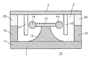
- FIG. 1 shows schematically the structure of a microoptical component 10 according to the invention .
- a toroid 14 made of SiO 2 is applied by means of a disk 13 on a foot 12 made of silicon, wherein the base 12 is firmly fixed to the first substrate 1, which likewise consists of silicon connected is. Furthermore, two side walls 15, 16 are attached to the first substrate 1 .
- On the second substrate 2 of quartz glass there are two rib waveguides 21, 22 made of PMMA.
- the second substrate 2 is provided with two side walls 25, 26 .
- an oxidized silicon wafer was first coated with a photoresist. Subsequently, the resist was using Electron beam lithography exposed and developed. The structured photoresist was used in the next step as an etching mask, wherein the glass was structured with buffered hydrofluoric acid. The photoresist was removed in the following step with acetone. Thereafter, the obtained slices were undercut with xenon difluoride to be melted in the last step by means of a CO 2 laser.
- an oxidized silicon wafer was first coated with a photoresist, which was then exposed by electron beam lithography and developed. Then, the obtained slices were undercut with xenon difluoride, finally to be melted by means of a hot plate.
- the first substrate 1 was provided with two side walls 15, 16 .
- the preparation of the rib waveguides from PMMA was carried out on a quartz glass substrate, onto which a layer of PMMA was spun on and the solvent was expelled in a subsequent baking step. Subsequently, the two waveguides were exposed by means of UV lithography with a chromium / quartz mask. In a second exposure step, the lithographic edges of the two waveguides were defined.
- the waveguides were developed by means of a developer solution consisting of methyl isobutyl ketone (MIBK) and isopropanol (IPA) in a mixing ratio of 1: 1.
- MIBK methyl isobutyl ketone
- IPA isopropanol
- GG developer consisting of 20% de-ionized water, 60% 2- (2-butoxyethoxy) ethanol, 15% tetra-hydro-1-4-oxazine and 5% 2-aminoethanol
- BDG Stopper consisting of 20% de-ionized water, 80% 2- (2-butoxyethoxy) ethanol used.
- the waveguides were singulated with a wafer saw, with the saw cut being made at a distance of about 20 ⁇ m from the waveguide edge.
- the second substrate 2 was equipped with two side walls 25, 26 simultaneously with the production of the rib waveguides 21, 22 .
- the rib waveguides 21, 22 which are located on the second substrate 2 were then approximated by reversing the second substrate 2 according to the flip-chip principle to the plurality of microresonators located on the first substrate 1 .
- the vertical spacing of the two substrates was adjusted so that the overlap of the waveguide mode and the microresonator mode became maximum. In this way, the optical coupling of the laser light to the at least two microresonators was set as optimally as possible.
- the two side walls 25, 26 of the second substrate 2 have been approximated to the two side walls 15, 16 of the first substrate 1 so as to be fixedly connected together as shown in FIG .
- the microfluidic channel 3 was formed together with the first substrate 1 and the second substrate 2 .
Landscapes
- Physics & Mathematics (AREA)
- General Physics & Mathematics (AREA)
- Optics & Photonics (AREA)
- Engineering & Computer Science (AREA)
- Microelectronics & Electronic Packaging (AREA)
- Optical Integrated Circuits (AREA)
Abstract
Description
- Die Erfindung betrifft ein mikrooptisches Bauelement zur Ankopplung von Laserlicht an Mikroresonatoren und ein Verfahren zu seiner Herstellung.
- Die Möglichkeit der Ankopplung von Laserlicht an einzelne Mikroresonatoren besitzt im Hinblick auf den Einsatz der Mikroresonatoren als Detektoren eine wichtige Bedeutung. A. M. Armani, R. P. Kulkarni, S. E. Fraser, R. C. Flagan und K. J. Vahala beschreiben in Label-Free, Single-Molecule Detection with Optical Microcavities, Science 317, S. 783-86, 2007, den markerfreien Nachweis von einzelnen Molekülen, die auf der Oberfläche eines Mikroresonators aufgebracht sind. Als Mikroresonator dient ein Toroid, der im Vergleich zu üblichen Resonatorgeometrien wie Scheiben oder Kugeln einen hohen Gütefaktor (Q-Faktor) besitzt. Der Toroid besteht aus Siliziumdioxid (SiO2) und steht auf einem Fuß aus Silizium (Si), der sich auf einem Substrat befindet, das ebenfalls aus Si besteht.
- D. K. Armani, T. J. Kippenberg, S. M. Spillane und K. J. Vahala beschreiben in Ultra-high-Q toroid microcavity on a chip, Nature 421, S. 925-28, 2003, die Ankopplung von Laserlicht an einzelne Mikroresonatoren durch ausgedünnte Glasfasern. Allerdings lässt sich damit die Ankopplung an mehr als zwei Mikroresonatoren nur schwer realisieren. Ursache hierfür ist der ausgedünnte Bereich der Glasfaser, der für die Ankopplung eingesetzt wird. Aufgrund des geringen Durchmessers der Glasfaser (ca. 1-2 µm) ist diese sehr empfindlich gegenüber mechanischer Belastung und der ausgedünnte Bereich ist bedingt durch die Herstellung nicht vollständig gerade. Somit ist es schwierig, den ausgedünnten Bereich der Glasfaser parallel zum Substrat auszurichten, ohne das Substrat zu berühren. Außerdem erfolgt innerhalb von 2-3 Tagen eine Degradation der Glasfaser.
- Q. Lai, W. Hunziker und H. Melchior stellen in Silica on Si waveguides for self-aligned fibre array coupling using flip-chip Si V-groove technique, Electronics Letters 32, S. 1916-1917, 1996, das so genannte Flip-Chip-Prinzip zur Stirnkopplung einer Glasfaser an Wellenleiter dar.
- Q. Liu, K. S. Chiang und K. P. Lor zeigen in Long-period gratings in polymer ridge waveguides, Optics Express 13, S. 1150-60, 2005, die Vorteile von polymeren Rippenwellenleitern gegenüber Rippenwellenleitern aus Glas oder aus Kristallen wie Lithiumniobat (LiNbO3) oder Silizium auf.
- In J. Laine, Design and Applications of Optical Microsphere Resonators, Dissertation, Helsinki University of Technology, S. 20-21, 2003, ist schematisch die Annäherung eines ersten Substrats, das einen Wellenleiter enthält, mittels des Flip-Chip-Prinzip an zwei Mikrosphären, die auf ein zweites Substrat aufgebracht sind, dargestellt. Über die relative Positionierung der beiden Substrate wird keine Aussage getätigt.
- Ausgehend hiervon ist es die Aufgabe der vorliegenden Erfindung, ein mikrooptisches Bauelement zur Ankopplung von Laserlicht an Mikroresonatoren und ein Verfahren zu seiner Herstellung vorzuschlagen, die die vorher genannten Nachteile und Einschränkungen nicht aufweisen.
- Insbesondere soll eine Vorrichtung bereitgestellt werden, die die Ankopplung von Laserlicht aus mindestens einem Wellenleiter an mehrere, vorzugsweise toroide Mikroresonatoren ermöglicht, wobei der mindestens eine Wellenleiter parallel zum Substrat mit den Mikroresonatoren ausgerichtet ist.
- Weiterhin soll eine Vorrichtung vorgeschlagen werden, die Mittel zur einfachen und definierten Zuführung einer nachzuweisenden Substanz in die Nachweiszone, in der sich die Mikroresonatoren befinden, bereitstellt.
- Schließlich soll ein Verfahren angegeben werden, mit dem sich der mindestens eine Wellenleiter, die mehreren Mikroresonatoren und die Mittel zur Zuführung der nachzuweisenden Substanz auf möglichst einfache Weise herstellen lassen.
- Diese Aufgabe wird gelöst im Hinblick auf das Bauelement durch die Merkmale des Anspruchs 1 und im Hinblick auf das Herstellungsverfahren durch die Schritte des Anspruchs 9. Die Unteransprüche beschreiben jeweils vorteilhafte Ausgestaltungen.
- Ein erfindungsgemäßes mikrooptisches Bauelement zur Ankopplung von Laserlicht an Mikroresonatoren besitzt zumindest die folgenden Bestandteile:
- mindestens einen Wellenleiter, bevorzugt einen oder zwei Wellenleiter zur Führung von Laserlicht,
- mindestens zwei Mikroresonatoren, die jeweils die Form eines sich auf einem Fuß befindlichen rotationssymmetrischen Körpers, bevorzugt eines Toroids oder Sphäroids (Rotationsellipsoid), der auch gebogen oder konisch ausgestaltet sein kann, aufweisen,
- ein erstes Substrat, auf dem sich die mindestens zwei Mikroresonatoren befinden und das auf zwei Seiten mit ersten Seitenwänden versehen ist,
- ein zweites, bevorzugt transparentes Substrat, auf dem sich der mindestens eine Wellenleiter befindet und das auf zwei Seiten mit zweiten Seitenwänden versehen ist,
- Erfindungsgemäß sind die ersten Seitenwände und die zweiten Seitenwände mechanisch fest miteinander verbunden.
- Der mindestens eine Wellenleiter, der zur Führung von Laserlicht geeignet ist, ist bevorzugt ein Rippenwellenleiter. Gemäß Liu et al. eignet sich hierzu vorzugsweise ein polymerer Rippenwellenleiter, insbesondere ein Rippenwellenleiter aus Polymethylmethacrylat (PMMA).
- Die mindestens zwei Mikroresonatoren weisen gemäß D. K. Armani et al. jeweils die Form eines sich auf einem Fuß befindlichen Sphäroids oder Toroids auf.
- Die optische Ankopplung des Laserlichts an die mindestens zwei Mikroresonatoren wird durch den mindestens einen Wellenleiter hergestellt, der sich auf dem zweiten Substrat befindet. Die Ankopplung des Laserlichts erfolgt hierbei nach dem so genannten Flip-Chip-Prinzip: Das Substrat mit dem mindestens einen Wellenleiter liegt umgedreht und von oben angenähert an den mindestens zwei Mikroresonatoren.
- Nimmt der laterale Abstand zwischen dem mindestens einen Wellenleiter und den mindestens zwei Mikroresonatoren einen Wert im Bereich der Wellenlänge des Lichtes, bevorzugt von 400 nm bis 3000 nm, an, koppelt das Laserlicht durch das seitliche evaneszente Feld des mindesten einen Wellenleiters in die mindestens zwei Mikroresonatoren ein. Der vertikale Abstand der beiden Substrate ist vorzugsweise so eingestellt, dass der Überlapp der Wellenleitermode und Mikroresonatormode maximal ist, wodurch die gewünschte optische Ankopplung des Laserlichts an die mindestens zwei Mikroresonatoren optimiert ist.
- Mit der vorliegenden Erfindung wird somit der mindestens eine Wellenleiter parallel zum ersten Substrat, worauf sich die mindestens zwei Mikroresonatoren befinden, ausgerichtet, ohne dass dieser die Mikroresonatoren oder das erste Substrat berührt. Diese Eigenschaft der vorliegenden Erfindung stellt die Voraussetzung für die gleichzeitige optische Ankopplung von Laserlicht an mindestens zwei Mikroresonatoren dar.
- In einer bevorzugten Ausgestaltung wird für das zweite Substrat ein transparentes Material, vorzugsweise Quarzglas oder PMMA ausgewählt, das darüber hinaus einen kleineren Brechungsindex als der mindestens eine Wellenleiter aufweist, so dass das Licht mittels Totalreflexion im mindestens einen Wellenleiter geführt werden kann.
- In einer besonderen Ausgestaltung sind zwei Wellenleiter vorgesehen, zwischen denen die mindestens zwei Mikroresonatoren angeordnet sind. Durch Platzierung eines zweiten Wellenleiters neben den mindestens zwei Mikroresonatoren eignet sich das Bauelement als schmalbandiges Add-/Drop-Filter in der optischen Telekommunikation, insbesondere um ausgewählte Frequenzen durch die mindestens zwei Mikroresonatoren zu filtern und in den zweiten Wellenleiter einzukoppeln.
- Erfindungsgemäß sind die ersten Seitenwände und die zweiten Seitenwände fest miteinander verbunden und müssen daher nicht relativ zueinander gehalten werden. Durch diese Befestigung ist auch eine passive Justage möglich. Vorzugsweise bestehen die beiden Seitenwände aus Silizium oder einem transparenten Material, bevorzugt Quarzglas oder einem Polymer.
- In einer besonders bevorzugten Ausgestaltung bilden die beiden Seitenwände zusammen mit beiden Substraten einen geschlossenen mikrofluidischen Kanal. Diese Anordnung ist im Hinblick auf die Verwendung der mindestens zwei Mikroresonatoren als Detektoren vorzugsweise dazu geeignet, um eine zu detektierende Substanz von außen mittels der im mikrofluidischen Kanal auftretenden Kapillarkräfte definiert in eine Nachweiszone im mikrofluidischen Kanal zu leiten.
- Ein erfindungsgemäßes mikrooptisches Bauelement lässt sich insbesondere mit dem folgenden Verfahren herstellen.
- Zur Herstellung der Mikrotoroide wird zunächst das erste Substrat mit einem Photoresist, der als Ätzmaske dient, belackt. Durch Belichtung und Entwicklung des Resists und anschließendes Aufschmelzen wird das Substrat derart strukturiert, dass mindestens zwei Mikroresonatoren, die jeweils in Form eines sich auf einem Fuß befindlichen rotationssymmetrischen Körpers ausgestaltet sind, ausgebildet werden.
- Zur Herstellung des mindestens einen Wellenleiters wird zunächst eine Schicht aus einem geeigneten Material auf das zweite Substrat aufgeschleudert. Nach entsprechender Belichtung und Entwicklung erfolgt eine Vereinzelung des mindestens einen Wellenleiters. Vorzugsweise wird auf diese Weise ein Rippenwellenleiter hergestellt.
- Erfindungsgemäß wird dann der mindestens eine Wellenleiter, der sich auf dem zweiten Substrat befindet, durch Umdrehen des zweiten Substrates gemäß dem Flip-Chip-Prinzip den mindestens zwei Mikroresonatoren angenähert. Für die Annäherung ist es vorteilhaft, dass das zweite Substrat transparent ist, um eine Justierung mittels eines Mikroskops vornehmen zu können.
- In einer bevorzugten Ausgestaltung werden die beiden Substrate dadurch fest miteinander verbunden, indem die Strukturierung der beiden Seitenwände jeweils in das Herstellungsverfahren eine jeden der beiden Substrate integriert ist. Diese Art der Ausgestaltung ist ein wesentlicher Vorteil gegenüber der sonst üblichen und aufwendigen Bonding-Technik.
- In einer besonders bevorzugten Ausgestaltung wird der mikrofluidische Kanal durch eine geeignete Verfahrensführung bei der Herstellung beider Substrate geformt, die vor der Flip-Chip-Annäherung durchgeführt wird. Anschließend werden die beiden Substrate fest miteinander verbunden.
- In einer alternativen Ausgestaltung wird der mikrofluidische Kanal durch den Einsatz eines zusätzlichen Materials, insbesondere von Klebstoff, der vorzugsweise Epoxidharz enthält, oder von Klebefolie, nach dem Flip-Chip-Prozess gebildet.
- Der wesentliche Vorteil eines erfindungsgemäßen mikrooptischen Bauelements liegt darin, dass die beiden Substrate fest miteinander verbunden sind und daher nicht relativ zueinander gehalten werden müssen. Diese Art der Befestigung ermöglicht es, auf einfache Weise einen mikrofluidischen Kanal zu realisieren und außerdem eine passive Justage durchzuführen.
- Im Gegensatz zur Glasfaser-Technik ist der mindestens eine Wellenleiter gerade und robust und lässt sich somit gleichzeitig an mehrere Mikroresonatoren parallel ankoppeln.
- Die Erfindung wird im Folgenden anhand von Ausführungsbeispielen mit Hilfe der Figur näher erläutert.
- Fig. 1 zeigt schematisch den Aufbau eines erfindungsgemäßen mikrooptischen Bauelements 10. Ein Toroid 14 aus SiO2 ist mittels einer Scheibe 13 auf einem Fuß 12 aus Silizium aufgebracht, wobei der Fuß 12 fest mit dem ersten Substrat 1, das ebenfalls aus Silizium besteht, fest verbunden ist. Weiterhin sind am ersten Substrat 1 zwei Seitenwände 15, 16 angebracht. Auf dem zweiten Substrat 2 aus Quarzglas befinden sich zwei Rippenwellenleiter 21, 22 aus PMMA. Außerdem ist das zweite Substrat 2 mit zwei Seitenwänden 25, 26 versehen.
- Zur Herstellung der als Mikrotoroide ausgestalteten Mikroresonatoren wurde zunächst ein oxidierter Silizium-Wafer mit einem Photoresist belackt. Anschließend wurde der Resist mittels Elektronenstrahl-Lithographie belichtet und entwickelt. Der strukturierte Photolack diente im nächsten Schritt als Ätzmaske, wobei das Glas mit gepufferter Flusssäure strukturiert wurde. Der Photolack wurde im folgenden Schritt mit Aceton entfernt. Danach wurden die erhaltenen Scheiben mit Xenondifluorid unterätzt, um im letzten Schritt mit Hilfe eines CO2-Lasers aufgeschmolzen zu werden.
- Alternativ wurde zunächst ein oxidierter Silizium-Wafer mit einem Photoresist belackt, der anschließend mittels Elektronenstrahl-Lithographie belichtet und entwickelt wurde. Dann wurden die erhaltenen Scheiben mit Xenondifluorid unterätzt, um schließlich mittels einer heißen Platte aufgeschmolzen zu werden.
- Gleichzeitig mit der Herstellung der Mikrotoroide wurde das erste Substrat 1 mit zwei Seitenwänden 15, 16 versehen.
- Die Herstellung der Rippenwellenleiter aus PMMA erfolgte auf einem Quarzglas-Substrat, auf das eine Schicht aus PMMA aufgeschleudert und das Lösungsmittel in einem anschließenden Backschritt ausgetrieben wurde. Anschließend wurden die beiden Wellenleiter.mittels UV-Lithographie mit einer Chrom/ Quarz-Maske belichtet. In einem zweiten Belichtungsschritt wurden die lithographischen Kanten der beiden Wellenleiter definiert.
- Im Anschluss erfolgte die Entwicklung der Wellenleiter mittels einer Entwicklerlösung, die aus Methylisobutylketon (MIBK) und Isopropanol (IPA) im Mischungsverhältnis 1:1 besteht. Alternativ wurde ein sog. GG-Entwickler, bestehend aus 20% de-ionisiertem Wasser, 60% 2-(2-butoxyethoxy) Ethanol, 15% Tetra-hydro-1-4-oxazine und 5% 2-Aminoethanol, und ein BDG-Stopper, bestehend aus 20% de-ionisiertem Wasser, 80% 2-(2-butoxyethoxy) Ethanol eingesetzt.
- Im letzten Schritt wurden die Wellenleiter mit einer Wafersäge vereinzelt, wobei der Sägeschnitt in einem Abstand von ca. 20 µm von der Wellenleiterkante erfolgte. Auch hier wurde das zweite Substrat 2 gleichzeitig mit der Herstellung der Rippenwellenleiter 21, 22 mit zwei Seitenwänden 25, 26 ausgestattet.
- Erfindungsgemäß wurden dann die Rippenwellenleiter 21, 22, die sich auf dem zweiten Substrat 2 befinden, durch Umdrehen des zweiten Substrats 2 gemäß dem Flip-Chip-Prinzip den mehreren Mikroresonatoren, die sich auf dem ersten Substrat 1 befanden, angenähert. Der vertikale Abstand der beiden Substrate wurde dabei so eingestellt, dass der Überlapp der Wellenleitermode und der Mikroresonatormode maximal wurde. Auf diese Weise wurde die optische Ankopplung des Laserlichts an die mindestens zwei Mikroresonatoren möglichst optimal eingestellt.
- Gleichzeitig mit dieser Annäherung wurden die beiden Seitenwände 25, 26 des zweiten Substrats 2 den beiden Seitenwänden 15, 16 des ersten Substrats 1 so angenähert, dass diese, wie in Fig. 1 dargestellt, fest miteinander verbunden wurden. Damit wurde zusammen mit dem ersten Substrat 1 und dem zweiten Substrat 2 der mikrofluidische Kanal 3 ausgebildet.
Claims (10)
- Mikrooptisches Bauelement (10) zur Ankopplung von Laserlicht an Mikroresonatoren, die mindestens einen Wellenleiter (21) für Laserlicht und mindestens zwei Mikroresonatoren, die jeweils in Form eines sich auf einem Fuß (12) befindlichen rotationssymmetrischen Körpers ausgestaltet sind, aufweisen, dadurch gekennzeichnet, dass die mindestens zwei Mikroresonatoren auf einem ersten Substrat (1), das mit ersten Seitenwänden (15, 16) versehen ist, und der mindestens eine Wellenleiter (21) auf einem zweiten Substrat (2), das mit zweiten Seitenwänden (25, 26) versehen ist, derart aufgebracht sind, dass die ersten Seitenwände (15, 16) und die zweiten Seitenwände (25, 36) fest miteinander verbunden sind.
- Mikrooptisches Bauelement nach Anspruch 1, dadurch gekennzeichnet, dass die ersten Seitenwände (15, 16) und die zweiten Seitenwände (15, 16) derart miteinander verbunden sind, dass sie einen mikrofluidischen Kanal (3) ausbilden, worin sich der mindestens eine Wellenleiter (21) und die mindestens zwei Mikroresonatoren befinden.
- Mikrooptisches Bauelement nach Anspruch 1 oder 2, dadurch gekennzeichnet, dass die beiden Seitenwände aus Silizium, Quarzglas oder einem transparenten Polymer bestehen.
- Mikrooptisches Bauelement nach einem der Ansprüche 1 bis 3, dadurch gekennzeichnet, dass das zweite Substrat (2) transparent ist und einen kleineren Brechungsindex als der mindestens seine Wellenleiter (21) aufweist.
- Mikrooptisches Bauelement nach einem der Ansprüche 1 bis 4, dadurch gekennzeichnet, dass der mindestens eine Wellenleiter (21)als polymerer Rippenwellenleiter ausgebildet ist.
- Mikrooptisches Bauelement nach einem der Ansprüche 1 bis 5, dadurch gekennzeichnet, dass zwei zur Einkopplung von Laserlicht geeigneten Wellenleiter (21, 22) vorgesehen sind, zwischen denen die mindestens zwei Mikroresonatoren angeordnet sind.
- Mikrooptisches Bauelement nach einem der Ansprüche 1 bis 6, dadurch gekennzeichnet, dass laterale Abstand zwischen dem mindestens einen Wellenleiter (21) und den mindestens zwei Mikroresonatoren von 400 nm bis 3000 nm beträgt.
- Mikrooptisches Bauelement nach einem der Ansprüche 1 bis 7, dadurch gekennzeichnet, dass die mindestens zwei Mikroresonatoren jeweils in Form eines sich auf einem Fuß (12) befindlichen Toroids (14) oder Sphäroids ausgestaltet sind.
- Verfahren zur Herstellung eines mikrooptischen Bauelements nach einem der Ansprüche 1 bis 8, dadurch gekennzeichnet, dass der mindestens eine Wellenleiter (21), der sich auf dem zweiten Substrat (2) befindet, durch Umdrehen des zweiten Substrates (2) den mindestens zwei Mikroresonatoren, die sich auf dem ersten Substrat (1) befinden, derart angenähert wird, dass sich gleichzeitig die beiden Seitenwände (25, 26) des zweiten Substrats (2) den beiden Seitenwänden (15, 16) des ersten Substrats (1) so annähern, dass sie fest miteinander verbunden werden.
- Mikrooptisches Bauelement nach Anspruch 9, dadurch gekennzeichnet, dass sich die beiden Seitenwände (25, 26) des zweiten Substrats (2) den beiden Seitenwänden (15, 16) des ersten Substrats (1) so annähern, dass sie zusammen mit dem ersten Substrat (1) und dem zweiten Substrat (2) den mikrofluidischen Kanal (3) ausbilden.
Priority Applications (2)
| Application Number | Priority Date | Filing Date | Title |
|---|---|---|---|
| EP09010782.2A EP2287592B1 (de) | 2009-08-22 | 2009-08-22 | Mikrooptisches Bauelement mit einem mikrofluidischen Kanal und Verfahren zu dessen Herstellung |
| US12/860,354 US8358884B2 (en) | 2009-08-22 | 2010-08-20 | Microoptical component and method for its manufacture |
Applications Claiming Priority (1)
| Application Number | Priority Date | Filing Date | Title |
|---|---|---|---|
| EP09010782.2A EP2287592B1 (de) | 2009-08-22 | 2009-08-22 | Mikrooptisches Bauelement mit einem mikrofluidischen Kanal und Verfahren zu dessen Herstellung |
Publications (2)
| Publication Number | Publication Date |
|---|---|
| EP2287592A1 true EP2287592A1 (de) | 2011-02-23 |
| EP2287592B1 EP2287592B1 (de) | 2014-11-12 |
Family
ID=41580084
Family Applications (1)
| Application Number | Title | Priority Date | Filing Date |
|---|---|---|---|
| EP09010782.2A Not-in-force EP2287592B1 (de) | 2009-08-22 | 2009-08-22 | Mikrooptisches Bauelement mit einem mikrofluidischen Kanal und Verfahren zu dessen Herstellung |
Country Status (2)
| Country | Link |
|---|---|
| US (1) | US8358884B2 (de) |
| EP (1) | EP2287592B1 (de) |
Cited By (2)
| Publication number | Priority date | Publication date | Assignee | Title |
|---|---|---|---|---|
| DE102011107360A1 (de) | 2011-06-29 | 2013-01-03 | Karlsruher Institut für Technologie | Mikrooptisches Element, mikrooptisches Array und optisches Sensorensystem |
| CN104792730A (zh) * | 2015-04-17 | 2015-07-22 | 山东大学 | 一种基于光波导激光结构的血糖浓度探测器及其制备方法与应用 |
Families Citing this family (4)
| Publication number | Priority date | Publication date | Assignee | Title |
|---|---|---|---|---|
| EP2581771A1 (de) * | 2011-10-14 | 2013-04-17 | Astrium Limited | Resonator mit verringerten Verlusten |
| DE102014012981A1 (de) * | 2014-09-02 | 2016-03-03 | Karlsruher Institut für Technologie | Vollpolymere Mikroresonatoren |
| WO2017115279A1 (en) * | 2015-12-28 | 2017-07-06 | Masdar Institute Of Science And Technology | A method to suspend an optical resonator in a fluid using segmented waveguides |
| US20230299550A1 (en) * | 2022-03-08 | 2023-09-21 | AOSense, Inc. | Low-strain mounting method for a transportable optical resonator |
Citations (8)
| Publication number | Priority date | Publication date | Assignee | Title |
|---|---|---|---|---|
| US5663790A (en) * | 1993-04-08 | 1997-09-02 | Pharmacia Biosensor Ab | Method and apparatus for determination of refractive index |
| WO2002008815A1 (en) * | 1999-12-07 | 2002-01-31 | California Institute Of Technology | Optical routing/switching based on control of waveguide-ring resonator coupling |
| US20050013529A1 (en) * | 2003-07-18 | 2005-01-20 | Chiu Raymond C. | Microring resonator and method for manufacturing |
| WO2005019798A2 (en) | 2003-08-13 | 2005-03-03 | The Regents Of The University Of Michigan | Biochemical sensors with micro-resonators |
| US20050162656A1 (en) * | 2004-01-27 | 2005-07-28 | Zhiping Zhou | Apparatus and method for detecting change of dielectric constant |
| WO2006108096A2 (en) * | 2005-04-06 | 2006-10-12 | President And Fellows Of Harvard College | Method and apparatus for measuring and monitoring distances, physical properties, and phase changes of light reflected from a surface based on a ring-resonator |
| US20070237460A1 (en) * | 2006-04-07 | 2007-10-11 | Xudong Fan | Hollow Core Optical Ring Resonator Sensor, Sensing Methods, and Methods of Fabrication |
| US20070269901A1 (en) * | 2002-10-02 | 2007-11-22 | Armani Andrea M | Biological and chemical microcavity resonant sensors and methods of detecting molecules |
Family Cites Families (1)
| Publication number | Priority date | Publication date | Assignee | Title |
|---|---|---|---|---|
| US566790A (en) * | 1896-09-01 | Half to james e |
-
2009
- 2009-08-22 EP EP09010782.2A patent/EP2287592B1/de not_active Not-in-force
-
2010
- 2010-08-20 US US12/860,354 patent/US8358884B2/en not_active Expired - Fee Related
Patent Citations (8)
| Publication number | Priority date | Publication date | Assignee | Title |
|---|---|---|---|---|
| US5663790A (en) * | 1993-04-08 | 1997-09-02 | Pharmacia Biosensor Ab | Method and apparatus for determination of refractive index |
| WO2002008815A1 (en) * | 1999-12-07 | 2002-01-31 | California Institute Of Technology | Optical routing/switching based on control of waveguide-ring resonator coupling |
| US20070269901A1 (en) * | 2002-10-02 | 2007-11-22 | Armani Andrea M | Biological and chemical microcavity resonant sensors and methods of detecting molecules |
| US20050013529A1 (en) * | 2003-07-18 | 2005-01-20 | Chiu Raymond C. | Microring resonator and method for manufacturing |
| WO2005019798A2 (en) | 2003-08-13 | 2005-03-03 | The Regents Of The University Of Michigan | Biochemical sensors with micro-resonators |
| US20050162656A1 (en) * | 2004-01-27 | 2005-07-28 | Zhiping Zhou | Apparatus and method for detecting change of dielectric constant |
| WO2006108096A2 (en) * | 2005-04-06 | 2006-10-12 | President And Fellows Of Harvard College | Method and apparatus for measuring and monitoring distances, physical properties, and phase changes of light reflected from a surface based on a ring-resonator |
| US20070237460A1 (en) * | 2006-04-07 | 2007-10-11 | Xudong Fan | Hollow Core Optical Ring Resonator Sensor, Sensing Methods, and Methods of Fabrication |
Non-Patent Citations (4)
| Title |
|---|
| AM ARMANI, RP KULKARNI, SE FRASER, RC FLAGAN, KJ VAHALA: "Label-free, single-molecule detection with optical microcavities", SCIENCE, vol. 317, 10 August 2007 (2007-08-10), pages 783 - 787, XP002566438 * |
| J. LAINE: "Resonators, Dissertation", 2003, HELSINKI UNIVERSITY OF TECHNOLOGY, article "Design and Applications of Optical Microsphere", pages: 20 - 21 |
| Q. LAI, W. HUNZIKER, H. MELCHIOR: "Silica on Si waveguides for self-aligned fibre array coupling using flip-chip Si V-groove technique", ELECTRONICS LETTERS, vol. 32, 1996, pages 1916 - 1917 |
| Q. LIU, K. S. CHIANG, K. P. LOR ZEIGEN: "Long-period gratings in polymer ridge waveguides", OPTICS EXPRESS, vol. 13, 2005, pages 1150 - 60 |
Cited By (4)
| Publication number | Priority date | Publication date | Assignee | Title |
|---|---|---|---|---|
| DE102011107360A1 (de) | 2011-06-29 | 2013-01-03 | Karlsruher Institut für Technologie | Mikrooptisches Element, mikrooptisches Array und optisches Sensorensystem |
| WO2013000553A1 (de) | 2011-06-29 | 2013-01-03 | Karlsruher Institut für Technologie | Mikrooptisches element, mikrooptisches array und optisches sensorsystem |
| US9176051B2 (en) | 2011-06-29 | 2015-11-03 | Karlsruher Institut Fuer Technologie | Micro-optical element, micro-optical array, and optical sensor system |
| CN104792730A (zh) * | 2015-04-17 | 2015-07-22 | 山东大学 | 一种基于光波导激光结构的血糖浓度探测器及其制备方法与应用 |
Also Published As
| Publication number | Publication date |
|---|---|
| US20110044581A1 (en) | 2011-02-24 |
| EP2287592B1 (de) | 2014-11-12 |
| US8358884B2 (en) | 2013-01-22 |
Similar Documents
| Publication | Publication Date | Title |
|---|---|---|
| DE69433402T2 (de) | Polymerische mikrostrukturen,die die kopplung zwischen einer optischen faser und einem wellenleiter vereinfachen | |
| EP2287592B1 (de) | Mikrooptisches Bauelement mit einem mikrofluidischen Kanal und Verfahren zu dessen Herstellung | |
| DE69839387T2 (de) | Optischer wellenleiterschaltkreis und ein diesen enthaltendes optisches wellenleitermodul | |
| DE112012003394B4 (de) | Photonisch integrierte Schaltungsvorrichtung und Verfahren zu dessen Herstellung, Kopplungssystem einer photonisch integrierten Schaltung und Kopplungseinheit eines photonischen Chip | |
| EP1250618B1 (de) | Verfahren zur herstellung einer gitterstruktur, optisches element, evaneszentfeldsensorplatte, mikrotiterplatte und nachrichtentechnischer optischer koppler sowie vorrichtung zur überwachung einer wellenlänge | |
| DE69816605T2 (de) | Verfahren zur herstellung eines optischen elements und optisches element daraus | |
| DE69917007T2 (de) | Wellenlänge multiplexer/demultilexer optische vorrichtung | |
| CH693368A5 (de) | Verfahren zur Herstellung eines Beugungsgitters, Lichtleiterbauteil sowie deren Verwendungen. | |
| DE102018110001A1 (de) | Optische schaltung und verfahren zum herstellen derselben | |
| DE69933651T2 (de) | Herstellung von diffraktionsgittern für optisches signal vorrichtungen und diese enthaltende optische signal vorrichtungen | |
| EP2219059A2 (de) | Verfahren zur Herstellung einer elektro-optischen Leiterplatte mit Lichtwellenleiterstrukturen | |
| EP0883825B1 (de) | Verfahren zur herstellung optischer bauelemente mit angekoppelten lichtwellenleitern und nach diesem verfahren hergestellte optische bauelemente | |
| EP0043475B1 (de) | Verfahren zur Herstellung einer integrierten mikrooptischen Vorrichtung zur Verwendung mit Multimode-Lichtfasern | |
| EP1715368B1 (de) | Verfahren zur Herstellung eines Bauteils zur optischen Kopplung | |
| DE112004000346T5 (de) | Passive Ausrichtung optischer Fasern mit optischen Elementen | |
| DE3011166A1 (de) | Verfahren zur herstellung einer optischen wellenleiteranordnung | |
| DE102015222328A1 (de) | Optische Komponente und Verfahren zu deren Herstellung | |
| WO1997028473A1 (de) | Verfahren zur herstellung von optischen bauelementen und optisches bauelement | |
| DE112019004628T5 (de) | Optische lichtleiter und verfahren zur die herstellung desselben | |
| DE102016015587B4 (de) | Substrat und dessen Herstellung | |
| DE102013204606A1 (de) | Wellenleiter-Resonator-Bauelement und Verfahren zu seiner Herstellung | |
| DE19523526C2 (de) | Mikrooptisches Bauelement | |
| DE4200396C1 (de) | ||
| EP2195692B1 (de) | Wellenleiteranordnung und integrierte optik mit herstellungsverfahren | |
| EP1090319A1 (de) | Optisches kopplungselement |
Legal Events
| Date | Code | Title | Description |
|---|---|---|---|
| PUAI | Public reference made under article 153(3) epc to a published international application that has entered the european phase |
Free format text: ORIGINAL CODE: 0009012 |
|
| AK | Designated contracting states |
Kind code of ref document: A1 Designated state(s): AT BE BG CH CY CZ DE DK EE ES FI FR GB GR HR HU IE IS IT LI LT LU LV MC MK MT NL NO PL PT RO SE SI SK SM TR |
|
| AX | Request for extension of the european patent |
Extension state: AL BA RS |
|
| APBK | Appeal reference recorded |
Free format text: ORIGINAL CODE: EPIDOSNREFNE |
|
| APBN | Date of receipt of notice of appeal recorded |
Free format text: ORIGINAL CODE: EPIDOSNNOA2E |
|
| APBR | Date of receipt of statement of grounds of appeal recorded |
Free format text: ORIGINAL CODE: EPIDOSNNOA3E |
|
| APBV | Interlocutory revision of appeal recorded |
Free format text: ORIGINAL CODE: EPIDOSNIRAPE |
|
| RIN1 | Information on inventor provided before grant (corrected) |
Inventor name: MAPPES, TIMO DR. Inventor name: HAUSER, MARIO Inventor name: KALT, HEINZ PROF. Inventor name: BECK, THORSTEN Inventor name: VANNAHME, CHRISTOPH Inventor name: GROSSMAN, TOBIAS |
|
| RIN1 | Information on inventor provided before grant (corrected) |
Inventor name: GROSSMANN, TOBIAS Inventor name: VANNAHME, CHRISTOPH Inventor name: BECK, TORSTEN Inventor name: MAPPES, TIMO DR. Inventor name: KALT, HEINZ PROF. Inventor name: HAUSER, MARIO |
|
| RIN1 | Information on inventor provided before grant (corrected) |
Inventor name: GROSSMANN, TOBIAS Inventor name: MAPPES, TIMO DR. Inventor name: BECK, TORSTEN Inventor name: HAUSER, MARIO Inventor name: KALT, HEINZ PROF. Inventor name: VANNAHME, CHRISTOPH |
|
| 17P | Request for examination filed |
Effective date: 20110617 |
|
| 17Q | First examination report despatched |
Effective date: 20110726 |
|
| REG | Reference to a national code |
Ref country code: DE Ref legal event code: R079 Ref document number: 502009010198 Country of ref document: DE Free format text: PREVIOUS MAIN CLASS: G01N0021550000 Ipc: G02B0006293000 |
|
| GRAP | Despatch of communication of intention to grant a patent |
Free format text: ORIGINAL CODE: EPIDOSNIGR1 |
|
| RIC1 | Information provided on ipc code assigned before grant |
Ipc: G01N 21/77 20060101ALI20140506BHEP Ipc: G01N 21/55 20140101ALI20140506BHEP Ipc: G02B 6/293 20060101AFI20140506BHEP Ipc: G02B 6/12 20060101ALI20140506BHEP |
|
| INTG | Intention to grant announced |
Effective date: 20140603 |
|
| GRAS | Grant fee paid |
Free format text: ORIGINAL CODE: EPIDOSNIGR3 |
|
| GRAA | (expected) grant |
Free format text: ORIGINAL CODE: 0009210 |
|
| AK | Designated contracting states |
Kind code of ref document: B1 Designated state(s): AT BE BG CH CY CZ DE DK EE ES FI FR GB GR HR HU IE IS IT LI LT LU LV MC MK MT NL NO PL PT RO SE SI SK SM TR |
|
| REG | Reference to a national code |
Ref country code: GB Ref legal event code: FG4D Free format text: NOT ENGLISH |
|
| REG | Reference to a national code |
Ref country code: CH Ref legal event code: NV Representative=s name: ROTTMANN, ZIMMERMANN + PARTNER AG, CH Ref country code: CH Ref legal event code: EP |
|
| REG | Reference to a national code |
Ref country code: AT Ref legal event code: REF Ref document number: 696081 Country of ref document: AT Kind code of ref document: T Effective date: 20141115 |
|
| REG | Reference to a national code |
Ref country code: IE Ref legal event code: FG4D Free format text: LANGUAGE OF EP DOCUMENT: GERMAN |
|
| REG | Reference to a national code |
Ref country code: DE Ref legal event code: R096 Ref document number: 502009010198 Country of ref document: DE Effective date: 20141224 |
|
| REG | Reference to a national code |
Ref country code: NL Ref legal event code: VDEP Effective date: 20141112 |
|
| PG25 | Lapsed in a contracting state [announced via postgrant information from national office to epo] |
Ref country code: ES Free format text: LAPSE BECAUSE OF FAILURE TO SUBMIT A TRANSLATION OF THE DESCRIPTION OR TO PAY THE FEE WITHIN THE PRESCRIBED TIME-LIMIT Effective date: 20141112 Ref country code: LT Free format text: LAPSE BECAUSE OF FAILURE TO SUBMIT A TRANSLATION OF THE DESCRIPTION OR TO PAY THE FEE WITHIN THE PRESCRIBED TIME-LIMIT Effective date: 20141112 Ref country code: PT Free format text: LAPSE BECAUSE OF FAILURE TO SUBMIT A TRANSLATION OF THE DESCRIPTION OR TO PAY THE FEE WITHIN THE PRESCRIBED TIME-LIMIT Effective date: 20150312 Ref country code: NO Free format text: LAPSE BECAUSE OF FAILURE TO SUBMIT A TRANSLATION OF THE DESCRIPTION OR TO PAY THE FEE WITHIN THE PRESCRIBED TIME-LIMIT Effective date: 20150212 Ref country code: IS Free format text: LAPSE BECAUSE OF FAILURE TO SUBMIT A TRANSLATION OF THE DESCRIPTION OR TO PAY THE FEE WITHIN THE PRESCRIBED TIME-LIMIT Effective date: 20150312 Ref country code: NL Free format text: LAPSE BECAUSE OF FAILURE TO SUBMIT A TRANSLATION OF THE DESCRIPTION OR TO PAY THE FEE WITHIN THE PRESCRIBED TIME-LIMIT Effective date: 20141112 Ref country code: FI Free format text: LAPSE BECAUSE OF FAILURE TO SUBMIT A TRANSLATION OF THE DESCRIPTION OR TO PAY THE FEE WITHIN THE PRESCRIBED TIME-LIMIT Effective date: 20141112 |
|
| PG25 | Lapsed in a contracting state [announced via postgrant information from national office to epo] |
Ref country code: SE Free format text: LAPSE BECAUSE OF FAILURE TO SUBMIT A TRANSLATION OF THE DESCRIPTION OR TO PAY THE FEE WITHIN THE PRESCRIBED TIME-LIMIT Effective date: 20141112 Ref country code: CY Free format text: LAPSE BECAUSE OF FAILURE TO SUBMIT A TRANSLATION OF THE DESCRIPTION OR TO PAY THE FEE WITHIN THE PRESCRIBED TIME-LIMIT Effective date: 20141112 Ref country code: GR Free format text: LAPSE BECAUSE OF FAILURE TO SUBMIT A TRANSLATION OF THE DESCRIPTION OR TO PAY THE FEE WITHIN THE PRESCRIBED TIME-LIMIT Effective date: 20150213 Ref country code: LV Free format text: LAPSE BECAUSE OF FAILURE TO SUBMIT A TRANSLATION OF THE DESCRIPTION OR TO PAY THE FEE WITHIN THE PRESCRIBED TIME-LIMIT Effective date: 20141112 Ref country code: PL Free format text: LAPSE BECAUSE OF FAILURE TO SUBMIT A TRANSLATION OF THE DESCRIPTION OR TO PAY THE FEE WITHIN THE PRESCRIBED TIME-LIMIT Effective date: 20141112 Ref country code: HR Free format text: LAPSE BECAUSE OF FAILURE TO SUBMIT A TRANSLATION OF THE DESCRIPTION OR TO PAY THE FEE WITHIN THE PRESCRIBED TIME-LIMIT Effective date: 20141112 |
|
| PG25 | Lapsed in a contracting state [announced via postgrant information from national office to epo] |
Ref country code: DK Free format text: LAPSE BECAUSE OF FAILURE TO SUBMIT A TRANSLATION OF THE DESCRIPTION OR TO PAY THE FEE WITHIN THE PRESCRIBED TIME-LIMIT Effective date: 20141112 Ref country code: RO Free format text: LAPSE BECAUSE OF FAILURE TO SUBMIT A TRANSLATION OF THE DESCRIPTION OR TO PAY THE FEE WITHIN THE PRESCRIBED TIME-LIMIT Effective date: 20141112 Ref country code: CZ Free format text: LAPSE BECAUSE OF FAILURE TO SUBMIT A TRANSLATION OF THE DESCRIPTION OR TO PAY THE FEE WITHIN THE PRESCRIBED TIME-LIMIT Effective date: 20141112 Ref country code: EE Free format text: LAPSE BECAUSE OF FAILURE TO SUBMIT A TRANSLATION OF THE DESCRIPTION OR TO PAY THE FEE WITHIN THE PRESCRIBED TIME-LIMIT Effective date: 20141112 Ref country code: SK Free format text: LAPSE BECAUSE OF FAILURE TO SUBMIT A TRANSLATION OF THE DESCRIPTION OR TO PAY THE FEE WITHIN THE PRESCRIBED TIME-LIMIT Effective date: 20141112 |
|
| REG | Reference to a national code |
Ref country code: DE Ref legal event code: R097 Ref document number: 502009010198 Country of ref document: DE |
|
| PLBE | No opposition filed within time limit |
Free format text: ORIGINAL CODE: 0009261 |
|
| STAA | Information on the status of an ep patent application or granted ep patent |
Free format text: STATUS: NO OPPOSITION FILED WITHIN TIME LIMIT |
|
| 26N | No opposition filed |
Effective date: 20150813 |
|
| PGFP | Annual fee paid to national office [announced via postgrant information from national office to epo] |
Ref country code: CH Payment date: 20150824 Year of fee payment: 7 Ref country code: GB Payment date: 20150824 Year of fee payment: 7 Ref country code: DE Payment date: 20150820 Year of fee payment: 7 |
|
| PG25 | Lapsed in a contracting state [announced via postgrant information from national office to epo] |
Ref country code: IT Free format text: LAPSE BECAUSE OF FAILURE TO SUBMIT A TRANSLATION OF THE DESCRIPTION OR TO PAY THE FEE WITHIN THE PRESCRIBED TIME-LIMIT Effective date: 20141112 |
|
| PG25 | Lapsed in a contracting state [announced via postgrant information from national office to epo] |
Ref country code: SI Free format text: LAPSE BECAUSE OF FAILURE TO SUBMIT A TRANSLATION OF THE DESCRIPTION OR TO PAY THE FEE WITHIN THE PRESCRIBED TIME-LIMIT Effective date: 20141112 |
|
| PG25 | Lapsed in a contracting state [announced via postgrant information from national office to epo] |
Ref country code: LU Free format text: LAPSE BECAUSE OF FAILURE TO SUBMIT A TRANSLATION OF THE DESCRIPTION OR TO PAY THE FEE WITHIN THE PRESCRIBED TIME-LIMIT Effective date: 20150822 Ref country code: MC Free format text: LAPSE BECAUSE OF FAILURE TO SUBMIT A TRANSLATION OF THE DESCRIPTION OR TO PAY THE FEE WITHIN THE PRESCRIBED TIME-LIMIT Effective date: 20141112 |
|
| REG | Reference to a national code |
Ref country code: IE Ref legal event code: MM4A |
|
| REG | Reference to a national code |
Ref country code: FR Ref legal event code: ST Effective date: 20160429 |
|
| PG25 | Lapsed in a contracting state [announced via postgrant information from national office to epo] |
Ref country code: IE Free format text: LAPSE BECAUSE OF NON-PAYMENT OF DUE FEES Effective date: 20150822 |
|
| PG25 | Lapsed in a contracting state [announced via postgrant information from national office to epo] |
Ref country code: FR Free format text: LAPSE BECAUSE OF NON-PAYMENT OF DUE FEES Effective date: 20150831 |
|
| REG | Reference to a national code |
Ref country code: AT Ref legal event code: MM01 Ref document number: 696081 Country of ref document: AT Kind code of ref document: T Effective date: 20150822 |
|
| REG | Reference to a national code |
Ref country code: CH Ref legal event code: PCAR Free format text: NEW ADDRESS: GARTENSTRASSE 28 A, 5400 BADEN (CH) |
|
| PG25 | Lapsed in a contracting state [announced via postgrant information from national office to epo] |
Ref country code: AT Free format text: LAPSE BECAUSE OF NON-PAYMENT OF DUE FEES Effective date: 20150822 |
|
| REG | Reference to a national code |
Ref country code: DE Ref legal event code: R119 Ref document number: 502009010198 Country of ref document: DE |
|
| PG25 | Lapsed in a contracting state [announced via postgrant information from national office to epo] |
Ref country code: MT Free format text: LAPSE BECAUSE OF FAILURE TO SUBMIT A TRANSLATION OF THE DESCRIPTION OR TO PAY THE FEE WITHIN THE PRESCRIBED TIME-LIMIT Effective date: 20141112 |
|
| REG | Reference to a national code |
Ref country code: CH Ref legal event code: PL |
|
| GBPC | Gb: european patent ceased through non-payment of renewal fee |
Effective date: 20160822 |
|
| PG25 | Lapsed in a contracting state [announced via postgrant information from national office to epo] |
Ref country code: LI Free format text: LAPSE BECAUSE OF NON-PAYMENT OF DUE FEES Effective date: 20160831 Ref country code: CH Free format text: LAPSE BECAUSE OF NON-PAYMENT OF DUE FEES Effective date: 20160831 |
|
| PG25 | Lapsed in a contracting state [announced via postgrant information from national office to epo] |
Ref country code: SM Free format text: LAPSE BECAUSE OF FAILURE TO SUBMIT A TRANSLATION OF THE DESCRIPTION OR TO PAY THE FEE WITHIN THE PRESCRIBED TIME-LIMIT Effective date: 20141112 Ref country code: BG Free format text: LAPSE BECAUSE OF FAILURE TO SUBMIT A TRANSLATION OF THE DESCRIPTION OR TO PAY THE FEE WITHIN THE PRESCRIBED TIME-LIMIT Effective date: 20141112 Ref country code: HU Free format text: LAPSE BECAUSE OF FAILURE TO SUBMIT A TRANSLATION OF THE DESCRIPTION OR TO PAY THE FEE WITHIN THE PRESCRIBED TIME-LIMIT; INVALID AB INITIO Effective date: 20090822 |
|
| PG25 | Lapsed in a contracting state [announced via postgrant information from national office to epo] |
Ref country code: BE Free format text: LAPSE BECAUSE OF NON-PAYMENT OF DUE FEES Effective date: 20150831 Ref country code: DE Free format text: LAPSE BECAUSE OF NON-PAYMENT OF DUE FEES Effective date: 20170301 Ref country code: GB Free format text: LAPSE BECAUSE OF NON-PAYMENT OF DUE FEES Effective date: 20160822 |
|
| PG25 | Lapsed in a contracting state [announced via postgrant information from national office to epo] |
Ref country code: TR Free format text: LAPSE BECAUSE OF FAILURE TO SUBMIT A TRANSLATION OF THE DESCRIPTION OR TO PAY THE FEE WITHIN THE PRESCRIBED TIME-LIMIT Effective date: 20141112 |
|
| PG25 | Lapsed in a contracting state [announced via postgrant information from national office to epo] |
Ref country code: MK Free format text: LAPSE BECAUSE OF FAILURE TO SUBMIT A TRANSLATION OF THE DESCRIPTION OR TO PAY THE FEE WITHIN THE PRESCRIBED TIME-LIMIT Effective date: 20141112 |