EP2286180B1 - Measuring the shape and thickness variation of a wafer with high slopes - Google Patents
Measuring the shape and thickness variation of a wafer with high slopes Download PDFInfo
- Publication number
- EP2286180B1 EP2286180B1 EP09747614.7A EP09747614A EP2286180B1 EP 2286180 B1 EP2286180 B1 EP 2286180B1 EP 09747614 A EP09747614 A EP 09747614A EP 2286180 B1 EP2286180 B1 EP 2286180B1
- Authority
- EP
- European Patent Office
- Prior art keywords
- wafer
- tilted
- wafer holder
- phase
- interferograms
- Prior art date
- Legal status (The legal status is an assumption and is not a legal conclusion. Google has not performed a legal analysis and makes no representation as to the accuracy of the status listed.)
- Active
Links
Images


Classifications
-
- G—PHYSICS
- G01—MEASURING; TESTING
- G01B—MEASURING LENGTH, THICKNESS OR SIMILAR LINEAR DIMENSIONS; MEASURING ANGLES; MEASURING AREAS; MEASURING IRREGULARITIES OF SURFACES OR CONTOURS
- G01B11/00—Measuring arrangements characterised by the use of optical techniques
- G01B11/24—Measuring arrangements characterised by the use of optical techniques for measuring contours or curvatures
- G01B11/2441—Measuring arrangements characterised by the use of optical techniques for measuring contours or curvatures using interferometry
-
- G—PHYSICS
- G01—MEASURING; TESTING
- G01B—MEASURING LENGTH, THICKNESS OR SIMILAR LINEAR DIMENSIONS; MEASURING ANGLES; MEASURING AREAS; MEASURING IRREGULARITIES OF SURFACES OR CONTOURS
- G01B11/00—Measuring arrangements characterised by the use of optical techniques
- G01B11/02—Measuring arrangements characterised by the use of optical techniques for measuring length, width or thickness
- G01B11/06—Measuring arrangements characterised by the use of optical techniques for measuring length, width or thickness for measuring thickness ; e.g. of sheet material
-
- G—PHYSICS
- G01—MEASURING; TESTING
- G01B—MEASURING LENGTH, THICKNESS OR SIMILAR LINEAR DIMENSIONS; MEASURING ANGLES; MEASURING AREAS; MEASURING IRREGULARITIES OF SURFACES OR CONTOURS
- G01B11/00—Measuring arrangements characterised by the use of optical techniques
- G01B11/30—Measuring arrangements characterised by the use of optical techniques for measuring roughness or irregularity of surfaces
-
- G—PHYSICS
- G01—MEASURING; TESTING
- G01B—MEASURING LENGTH, THICKNESS OR SIMILAR LINEAR DIMENSIONS; MEASURING ANGLES; MEASURING AREAS; MEASURING IRREGULARITIES OF SURFACES OR CONTOURS
- G01B9/00—Measuring instruments characterised by the use of optical techniques
- G01B9/02—Interferometers
- G01B9/02015—Interferometers characterised by the beam path configuration
- G01B9/02017—Interferometers characterised by the beam path configuration with multiple interactions between the target object and light beams, e.g. beam reflections occurring from different locations
- G01B9/02021—Interferometers characterised by the beam path configuration with multiple interactions between the target object and light beams, e.g. beam reflections occurring from different locations contacting different faces of object, e.g. opposite faces
-
- G—PHYSICS
- G01—MEASURING; TESTING
- G01B—MEASURING LENGTH, THICKNESS OR SIMILAR LINEAR DIMENSIONS; MEASURING ANGLES; MEASURING AREAS; MEASURING IRREGULARITIES OF SURFACES OR CONTOURS
- G01B9/00—Measuring instruments characterised by the use of optical techniques
- G01B9/02—Interferometers
- G01B9/02015—Interferometers characterised by the beam path configuration
- G01B9/02027—Two or more interferometric channels or interferometers
- G01B9/02028—Two or more reference or object arms in one interferometer
-
- G—PHYSICS
- G01—MEASURING; TESTING
- G01B—MEASURING LENGTH, THICKNESS OR SIMILAR LINEAR DIMENSIONS; MEASURING ANGLES; MEASURING AREAS; MEASURING IRREGULARITIES OF SURFACES OR CONTOURS
- G01B2290/00—Aspects of interferometers not specifically covered by any group under G01B9/02
- G01B2290/45—Multiple detectors for detecting interferometer signals
Definitions
- This application relates to radiation-based inspection techniques and more particularly to interferometric profilometry systems and methods which may be used to measure the shape, and thickness variation of a wafer with high slopes.
- Described herein are exemplary systems and methods which may be used to measure the surface height on both sides and the thickness variation of a wafer with high surface slopes.
- numerous specific details are set forth in order to provide a thorough understanding of various embodiments. However, it will be understood by those skilled in the art that the various embodiments may be practiced without the specific details. In other instances, well-known methods, procedures, components, and circuits have not been described in detail so as not to obscure the particular embodiments.
- Embodiments described herein may be used in conjunction with two unequal path length interferometers (such as Fizeau interferometers), contemporaneously acquiring two sets of intensity frames that record interferograms generated with wavefronts reflected from both sides of a wafer surfaces and from the reference flats. These intensity frames may be acquired sequentially, by changing the wavelength in a measurement system. The wavelength can be changed mechanically, or, preferably, with a tunable laser light source.
- the phrase contemporaneous events refers to events which happen within a reasonable time period of one another, given the technical circumstances.
- the methods described herein take advantage of the fact that the high spatial slope of the optical path difference (OPD) between a wafer surface and a reference flat can be locally nulled or reduced by changing tilt of the wafer.
- OPD optical path difference
- the interferogram moves around on the imaging plane or the measuring area of the wafer surface shifts if the tilt of the wafer changes. This is because an interferogram only appears at the area where spatial slope of OPD is small and the measurement is only accomplished at the area where the interferogram is visible.
- a map of partial wafer surface may be achieved from each measurement at a tilt position of the wafer. Multiple such maps that correspond to different parts of the wafer surface may be required to measure a wafer with high surface slopes.
- system and method of an embodiment of the invention may be able to produce a height map that covers a wafer surface with high slopes by combining multiple maps of partial wafer surface measurements.
- system and method of a preferred embodiment of the invention may be able to construct the surface height maps on a part of or whole wafer on both sides simultaneously and may be able to measure thickness variation of a wafer without errors results from the cavity path difference.
- the system and method of an embodiment of the invention employs two reference flats that are larger in size than the measuring wafer. While the center part of reference flats forms the interferograms with the wafer surfaces, their outside annular area generates the interferogram of themselves.
- the invention is not only able to determine the location of a testing wafer very precisely by finding out its shade on the reference flats but also is able to monitor the relative tilt change of reference flats with every measurement. Consequently, it is capable of measuring the wafer edge location without the influence of the surface slopes at the wafer edge thereby significantly increases the measurement repeatability.
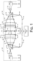
- Fig. 1 is a schematic illustration of an interferometer assembly according to embodiments.
- the unequal path interferometer may be a Fizeau interferometer.
- the unequal path interferometer may be a Twyman-Green interferometer.
- An overview of an embodiment of the invention is shown in Fig. 1 .
- a wafer 160 may be placed in a cavity in the center between two improved Fizeau interferometers 120 and 140, such that both wafer sides 161 and 162 are minimally obscured by the holding devices 172, 174.
- the interferometers 120 and 140 may operate in the following way: light is emitted from an illuminator 110 along fibers 122, 142, reflected at a polarizing beam splitter 126, 146 and passes through a quarter-wave plate 128, 148 aligned at 45 degrees to the polarization direction of the polarizing beam splitter 126, 146.
- Two multimode optic fibers 142 and 122 collect the light from the illuminator 110 and carry it to the two source locations 144 and 124 of the two interferometer channels 140 and 120. The light is circularly polarized after the quarter-wave plate. This beam then propogates to the lens 130, 150, where it is collimated with a beam diameter larger than the wafer diameter.
- the collimated beam then falls on the reference flat 132,152, where part of the light is reflected at the reference surface, and another part is transmitted.
- the central part of the transmitted beam is reflected at the test surface 161,162; and the outer part of the transmitted beam travels on to the opposite reference flat 152,132, where it is reflected at the reference surface 153,133.
- the light reflected at the wafer surface 161,162 constitutes the wafer test beam.
- the light reflected at the opposite reference surface 133,153 constitutes the cavity ring test beam; and the light reflected at the reference surface constitutes the reference beam. All three reflected beams travel back through the reference flat 152,132 and through the collimator lens 150,130 to the quarter-wave plate 148,128. After the quarter-wave plate, the beams are linearly polarized with the plane of polarization of the reflected beams rotated 90 degrees compared to the outgoing beams.
- the reflected beams When the reflected beams reach the beam splitter 146,126, they are transmitted and directed to an imaging lens 154,134, which relays the beams to a detector 156,136, where the interference patterns between the test beams (reflected from the wafer 160) and the reference beams occur.
- the detector 156,136 may consist of a video camera, the signal of which is digitized and further processed in a computer 158,138.
- the computers 158 and 138 of each interferometer channel are connected for data exchange and synchronization. Alternatively, one common computer could be used to receive the camera signals of both channels. Computers 158,138 are further discussed with reference to Fig. 3 .
- the data acquisition is now described in more detail for interferometer channel 140.
- the second interferometer channel 120 behaves in an equivalent way.
- the two reference surfaces 153, 133 and the wafer 160 are substantially parallel.
- the interference pattern appears on detector 156.
- wafer holding devices 172, 174 may be actively tilted by holding device motors 170,176 in a controlled way between data acquisitions to allow measurements of local areas on the wafer with high slopes.
- an area may be considered to have a high slope when a surface slopes greater than wavelength divided by twice w, where w is the pixel width.
- the wafer tilting may be performed to null the local high slopes in a region of interest of the wafer, which corresponds to a certain sensing area of the detectors 156,136. In such embodiments, predictions may be made as to what tilt may yield a complete dataset covering the full area of the wafer.
- a wafer with high surface slope may be measured by an adequate sequence of tilts of the wafer.
- the wafer holding devices 172 and 174 are a right body or can not move relatively. In such embodiments, the wafer holding devices 172 and 174 are always tilted together by either the holding device motors 170 or 176. This allows for the free shape of the wafer to be more accurately measured.
- any suitable wafer holding device may be used, with a preferred holder being a vertical wafer pallet minimizing the stress on the wafer to be held. In such embodiments, this may allow for the free shape of the wafer to be more accurately measured.
- the wafer holding device may be implemented by using two computer controlled piezo-actuated flexures allowing the angles to be precisely controlled.
- a phase-shifting data acquisition method is applied to extract the interferometric fringe phase.
- extracting phases of each of the interferograms may be effected by a computer.
- recording the multiple optical interferograms may be effected by means of a CCD camera.
- Fig. 2A is a flowchart illustrating operations of a method which may be used to measure the shape and thickness of a wafer with high slope areas according to an embodiment.
- an interferometer may be initiated.
- a test object such as, but not limited to, a wafer is placed in the interferometer.
- the interferometer may be a Fizeau interferometer, a Twyman-Green interferometer, or the like.
- coherent light is supplied to a test object.
- the coherent light may be supplied by a tunable laser or the like.
- an interferometer records interference patterns.
- recording the multiple optical interferograms may be effected by means of a CCD camera.
- phases for interferograms are extracted from data recorded by the interferometer.
- extracting phases of the interferograms from each channel of the interferometer may be effected by a computer.
- the process of extracting phases may be affected by two computers.
- analysis of these interferograms allows for the determination of various information, such as but not limited to, local areas of interest on the surface of the object that have high slopes. These areas of high slope do not produce height or thickness information as the reflected light returns at such an angle as it is not received by the detectors.
- the object surface is analyzed to determine in there are any areas of high slope which may require further analysis to determine their properties. If at operation 226, there are local areas of interest for additional analysis, then at operation 231 the wafer may be titled by the wafer holding devices. In operation, predictions may be made as to what tilt sequence may yield a complete dataset covering the full area of the wafer.
- additional interferograms are produced through repeating operations 206 to 216 until there are no longer unmeasured high slope areas. If at operation 226, there are no areas that may require additional analysis due to high slopes, then at operation 236 complete parameter maps of the object surface may be produced. In some embodiments, a computer may stitch together all partial surfaces that are taken at different tilts and partially overlap each other and thereby produce a measurement that covers the entire object surface.
- Additional information relating to the wafer properties may be obtained through analysis of phase maps obtained from the interferograms.
- the surface parameters may be determined as follows: A corresponds to the front surface height of the wafer, B corresponds to the back surface height of the wafer, C-(A+B) corresponds to the thickness variation in the wafer.
- Fig. 2B is a flowchart illustrating operations of a method which may be used to measure the shape and thickness variation of a wafer according to an embodiment.
- the laser is activated at a first wavelength.
- the laser 110 generates electromagnetic radiation in a range of wavelengths to interferometer 120,140.
- radiation reflected is captured.
- radiation reflected is captured as the wavelength of radiation is changing.
- the reflected radiation is directed by interferometer 120,140, contemporaneously, multiple interferograms to detector 136,156 (e.g., a CCD camera or other suitable recording planes).
- contemporaneous events may be defined as events that occur within a reasonable time period of one another, given the technical circumstances.
- the detector 136,156 may include a frame grabber for storing images; alternatively, the computer 138,158 may be configured to provide this function. In any event, the images obtained by the detector 136,156 are supplied to the computer 138,158 for processing to produce the desired profiles in a suitable form for immediate display, or storage for subsequent utilization.
- interference patterns in the reflected radiation are captured.
- one or more parameters are determined from the phases obtained in operation 230.
- the surface parameters may be determined as follows: A corresponds to the front surface height of the wafer 160, B corresponds to the back surface height of the wafer, C-(A+B) corresponds to the thickness variation in the wafer 160.
- parameter maps for the entire object may be produced.
- a computer may stitch together all partial surfaces that overlap each other and thereby produce a measurement that covers the entire object surface.
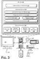
- Fig. 3 is a schematic illustration of one embodiment of a computing system which may be used to implement the computer 138,158 of Fig. 1 .
- the computer system 300 includes a computer 308 and one or more accompanying input/output devices 306 including a display 302 having a screen 304, a keyboard 310, other I/O device(s) 312, and a mouse 314.
- the other device(s) 312 can include a touch screen, a voice-activated input device, a track ball, and any other device that allows the system 300 to receive input from a developer and/or a user.
- the computer 308 includes system hardware 320 and random access memory and/or read-only memory 330.
- a file store 380 is communicatively connected to computer 308.
- File store 380 may be internal such as, e.g., one or more hard drives, or external such as, e.g., one or more external hard drives, network attached storage, or a separate storage network.
- Memory 330 includes an operating system 340 for managing operations of computer 308.
- operating system 340 includes a hardware interface module 354 that provides an interface to system hardware 320.
- operating system 340 includes one or more file systems 350 that manage files used in the operation of computer 308 and a process control subsystem 352 that manages processes executing on computer 308.
- Operating system 340 further includes a system call interface module 342 that provides an interface between the operating system 340 and one or more application modules 362.
- one or more application modules and/or libraries executing on computer 308 make calls to the system call interface module 342 to execute one or more commands on the computer's processor.
- the system call interface module 342 invokes the services of the file system(s) 350 to manage the files required by the command(s) and the process control subsystem 352 to manage the process required by the command(s).
- the file system(s) 350 and the process control subsystem 352 in turn, invoke the services of the hardware interface module 354 to interface with the system hardware 320.
- Operating system 340 may be embodied as a UNIX operating system or any derivative thereof (e.g., Linux, Solaris, etc.) or as a Windows® brand operating system.
- computer system 300 includes one or more modules to implement hybrid database query caching.
- computer system 300 includes a surface analysis module 362 which implements the operations described with reference to Fig. 2A and Fig. 2B .
Landscapes
- Physics & Mathematics (AREA)
- General Physics & Mathematics (AREA)
- Instruments For Measurement Of Length By Optical Means (AREA)
- Length Measuring Devices By Optical Means (AREA)
Description
- This application relates to radiation-based inspection techniques and more particularly to interferometric profilometry systems and methods which may be used to measure the shape, and thickness variation of a wafer with high slopes.
-
-
Fig. 1 is a schematic illustration of an interferometer assembly according to embodiments. -
Fig. 2A is a flowchart illustrating operations of a method which may be used to measure the shape and thickness of a wafer with high slopes according to an embodiment. -
Fig. 2B is a flowchart illustrating operations of a method which may be used to measure the shape and thickness of a wafer with high slopes according to an embodiment. -
Fig. 3 is a schematic illustration of an integrated visible pilot beam for non-visible interferometric device according to an embodiment. - The invention is defined by the independent claims. Embodiments of the invention are set out in the dependent claims.
- Described herein are exemplary systems and methods which may be used to measure the surface height on both sides and the thickness variation of a wafer with high surface slopes. In the following description, numerous specific details are set forth in order to provide a thorough understanding of various embodiments. However, it will be understood by those skilled in the art that the various embodiments may be practiced without the specific details. In other instances, well-known methods, procedures, components, and circuits have not been described in detail so as not to obscure the particular embodiments.
- Embodiments described herein may be used in conjunction with two unequal path length interferometers (such as Fizeau interferometers), contemporaneously acquiring two sets of intensity frames that record interferograms generated with wavefronts reflected from both sides of a wafer surfaces and from the reference flats. These intensity frames may be acquired sequentially, by changing the wavelength in a measurement system. The wavelength can be changed mechanically, or, preferably, with a tunable laser light source. As used herein, the phrase contemporaneous events refers to events which happen within a reasonable time period of one another, given the technical circumstances. As used herein, the term "contemporaneous" should not be construed to mean "simultaneous." Embodiments of an interferometer assembly for contemporaneous acquisition of multiple sets of intensity frames are described in
U.S. Patent No. 6,847,458 to Freischlad, et al. , entitled METHOD AND APPARATUS FOR MEASURING THE SHAPE AND THICKNESS VARIATION OF POLISHED OPAQUE PLATES. - In general, the methods described herein take advantage of the fact that the high spatial slope of the optical path difference (OPD) between a wafer surface and a reference flat can be locally nulled or reduced by changing tilt of the wafer. This implies that the interferogram moves around on the imaging plane or the measuring area of the wafer surface shifts if the tilt of the wafer changes. This is because an interferogram only appears at the area where spatial slope of OPD is small and the measurement is only accomplished at the area where the interferogram is visible. A map of partial wafer surface may be achieved from each measurement at a tilt position of the wafer. Multiple such maps that correspond to different parts of the wafer surface may be required to measure a wafer with high surface slopes.
- In general, the system and method of an embodiment of the invention may be able to produce a height map that covers a wafer surface with high slopes by combining multiple maps of partial wafer surface measurements.
- In general, the system and method of a preferred embodiment of the invention may be able to construct the surface height maps on a part of or whole wafer on both sides simultaneously and may be able to measure thickness variation of a wafer without errors results from the cavity path difference.
- In general, the system and method of an embodiment of the invention employs two reference flats that are larger in size than the measuring wafer. While the center part of reference flats forms the interferograms with the wafer surfaces, their outside annular area generates the interferogram of themselves. In some embodiments, the invention is not only able to determine the location of a testing wafer very precisely by finding out its shade on the reference flats but also is able to monitor the relative tilt change of reference flats with every measurement. Consequently, it is capable of measuring the wafer edge location without the influence of the surface slopes at the wafer edge thereby significantly increases the measurement repeatability.
-
Fig. 1 is a schematic illustration of an interferometer assembly according to embodiments. In some embodiments, the unequal path interferometer may be a Fizeau interferometer. In some embodiments, the unequal path interferometer may be a Twyman-Green interferometer. An overview of an embodiment of the invention is shown inFig. 1 . For wafer measurement, awafer 160 may be placed in a cavity in the center between two improved Fizeauinterferometers wafer sides holding devices interferometers illuminator 110 alongfibers beam splitter wave plate beam splitter optic fibers illuminator 110 and carry it to the twosource locations interferometer channels lens - The light reflected at the wafer surface 161,162 constitutes the wafer test beam. The light reflected at the opposite reference surface 133,153 constitutes the cavity ring test beam; and the light reflected at the reference surface constitutes the reference beam. All three reflected beams travel back through the reference flat 152,132 and through the collimator lens 150,130 to the quarter-wave plate 148,128. After the quarter-wave plate, the beams are linearly polarized with the plane of polarization of the reflected beams rotated 90 degrees compared to the outgoing beams. When the reflected beams reach the beam splitter 146,126, they are transmitted and directed to an imaging lens 154,134, which relays the beams to a detector 156,136, where the interference patterns between the test beams (reflected from the wafer 160) and the reference beams occur.
- The detector 156,136 may consist of a video camera, the signal of which is digitized and further processed in a computer 158,138. The
computers Fig. 3 . - The data acquisition is now described in more detail for
interferometer channel 140. Thesecond interferometer channel 120 behaves in an equivalent way. The tworeference surfaces wafer 160 are substantially parallel. Thus, the interference pattern appears ondetector 156. There is a central area of interference fringes imposed on the wafer surface, generated by interference of the wafer test beam, with the reference beam. In addition, there is an area surrounding thewafer 160 with interference fringes generated by the cavity ring test beam and the reference beam. Depending on the slopes of the wafer surfaces, there may be a zone without any interference fringes. This zone without fringes is caused by the test beam being reflected at such high angles that it does not reach the camera. - In some embodiments, wafer holding
devices wafer holding devices wafer holding devices device motors - In order to obtain height maps from the interference patterns, a phase-shifting data acquisition method is applied to extract the interferometric fringe phase. In some embodiments, extracting phases of each of the interferograms may be effected by a computer. In some embodiments, recording the multiple optical interferograms may be effected by means of a CCD camera.
-
Fig. 2A is a flowchart illustrating operations of a method which may be used to measure the shape and thickness of a wafer with high slope areas according to an embodiment. Atoperation 201, an interferometer may be initiated. In some embodiments, a test object such as, but not limited to, a wafer is placed in the interferometer. By way of example and not limitation, the interferometer may be a Fizeau interferometer, a Twyman-Green interferometer, or the like. Atoperation 206, coherent light is supplied to a test object. In some embodiments, the coherent light may be supplied by a tunable laser or the like. Atoperation 211, an interferometer records interference patterns. In some embodiments, recording the multiple optical interferograms may be effected by means of a CCD camera. Atoperation 216, phases for interferograms are extracted from data recorded by the interferometer. In some embodiments, extracting phases of the interferograms from each channel of the interferometer may be effected by a computer. In some embodiments, the process of extracting phases may be affected by two computers. - In some embodiments, analysis of these interferograms allows for the determination of various information, such as but not limited to, local areas of interest on the surface of the object that have high slopes. These areas of high slope do not produce height or thickness information as the reflected light returns at such an angle as it is not received by the detectors. At
operation 226, the object surface is analyzed to determine in there are any areas of high slope which may require further analysis to determine their properties. If atoperation 226, there are local areas of interest for additional analysis, then atoperation 231 the wafer may be titled by the wafer holding devices. In operation, predictions may be made as to what tilt sequence may yield a complete dataset covering the full area of the wafer. - Once the wafer has been tilted to the determined angle, additional interferograms are produced through repeating
operations 206 to 216 until there are no longer unmeasured high slope areas. If atoperation 226, there are no areas that may require additional analysis due to high slopes, then atoperation 236 complete parameter maps of the object surface may be produced. In some embodiments, a computer may stitch together all partial surfaces that are taken at different tilts and partially overlap each other and thereby produce a measurement that covers the entire object surface. - Additional information relating to the wafer properties may be obtained through analysis of phase maps obtained from the interferograms. By way of example and not limitation, arbitrarily identifying the phase of the interferogram formed by the front reference plate and the front of the wafer surface as A, and the phase of the interferogram formed by the back reference flat and the back surface of the wafer as B, and the phase of the interferogram formed by the cavity of the front reference flat and the back reference flat as C, then the surface parameters may be determined as follows: A corresponds to the front surface height of the wafer, B corresponds to the back surface height of the wafer, C-(A+B) corresponds to the thickness variation in the wafer.
-
Fig. 2B is a flowchart illustrating operations of a method which may be used to measure the shape and thickness variation of a wafer according to an embodiment. Atoperation 205 the laser is activated at a first wavelength. In operation, thelaser 110 generates electromagnetic radiation in a range of wavelengths to interferometer 120,140. - At
operation 210 radiation reflected is captured. In some embodiments, radiation reflected is captured as the wavelength of radiation is changing. The reflected radiation is directed by interferometer 120,140, contemporaneously, multiple interferograms to detector 136,156 (e.g., a CCD camera or other suitable recording planes). In some embodiments, contemporaneous events may be defined as events that occur within a reasonable time period of one another, given the technical circumstances. The detector 136,156 may include a frame grabber for storing images; alternatively, the computer 138,158 may be configured to provide this function. In any event, the images obtained by the detector 136,156 are supplied to the computer 138,158 for processing to produce the desired profiles in a suitable form for immediate display, or storage for subsequent utilization. Atoperation 215 interference patterns in the reflected radiation are captured. - If, at
operation 220, the amount of data acquired is not sufficient, then control passes tooperation 225 and the wavelength of the radiation generated bylaser 110 is changed. In some embodiments, if the amount of data acquired in not sufficient, the control passed tooperation 225 to keep changing its wavelength. For example, the wavelength may be increased or decreased by a predetermined amount. Control then passes back tooperation 210 and the reflected radiation is captured. Operations 210-225 are repeated until an adequate number of data samples are acquired, whereupon control passes tooperation 230 and one or more phases of interferograms are extracted from the data collected. In some embodiments, a control passed tooperation 225 to stop its wavelength changing while another control passed tooperation 230. In some embodiments, the phases of interferograms may be extracted and stored. - At
operation 235 one or more parameters are determined from the phases obtained inoperation 230. By way of example and not limitation, arbitrarily identifying the phase of the interferogram formed by thefront reference plate 133 and thefront 161 of thewafer 160 surface as A, and the phase of the interferogram formed by the back reference flat 1 53 and theback surface 162 of thewafer 160 as B, and the phase of the interferogram formed by the cavity of the front reference flat 133 and 153 as C, then the surface parameters may be determined as follows: A corresponds to the front surface height of thewafer 160, B corresponds to the back surface height of the wafer, C-(A+B) corresponds to the thickness variation in thewafer 160. - If at
operation 240, there are local areas on the object that have unmeasured parameters due to the high slope of the object at those locations, then atoperation 245 the object may be tilted.Operations 205 through 235 may then be performed until all local areas of interest with high slopes have been sufficiently mapped. - If at
operation 240, there are no additional local areas of interest with high slope, then atoperation 250 parameter maps for the entire object may be produced. In some embodiments, a computer may stitch together all partial surfaces that overlap each other and thereby produce a measurement that covers the entire object surface. -
Fig. 3 is a schematic illustration of one embodiment of a computing system which may be used to implement the computer 138,158 ofFig. 1 . Thecomputer system 300 includes acomputer 308 and one or more accompanying input/output devices 306 including adisplay 302 having ascreen 304, akeyboard 310, other I/O device(s) 312, and amouse 314. The other device(s) 312 can include a touch screen, a voice-activated input device, a track ball, and any other device that allows thesystem 300 to receive input from a developer and/or a user. Thecomputer 308 includessystem hardware 320 and random access memory and/or read-only memory 330. Afile store 380 is communicatively connected tocomputer 308.File store 380 may be internal such as, e.g., one or more hard drives, or external such as, e.g., one or more external hard drives, network attached storage, or a separate storage network. -
Memory 330 includes anoperating system 340 for managing operations ofcomputer 308. In one embodiment,operating system 340 includes ahardware interface module 354 that provides an interface tosystem hardware 320. In addition,operating system 340 includes one ormore file systems 350 that manage files used in the operation ofcomputer 308 and aprocess control subsystem 352 that manages processes executing oncomputer 308.Operating system 340 further includes a systemcall interface module 342 that provides an interface between theoperating system 340 and one ormore application modules 362. - In operation, one or more application modules and/or libraries executing on
computer 308 make calls to the systemcall interface module 342 to execute one or more commands on the computer's processor. The systemcall interface module 342 invokes the services of the file system(s) 350 to manage the files required by the command(s) and theprocess control subsystem 352 to manage the process required by the command(s). The file system(s) 350 and theprocess control subsystem 352, in turn, invoke the services of thehardware interface module 354 to interface with thesystem hardware 320. - The particular embodiment of
operating system 340 is not critical to the subject matter described herein.Operating system 340 may be embodied as a UNIX operating system or any derivative thereof (e.g., Linux, Solaris, etc.) or as a Windows® brand operating system. - In some embodiments,
computer system 300 includes one or more modules to implement hybrid database query caching. In the embodiment depicted inFig. 3 ,computer system 300 includes asurface analysis module 362 which implements the operations described with reference toFig. 2A andFig. 2B . - While the invention has been particularly shown and described with reference to a preferred embodiment and various alternate embodiments, it will be understood by persons skilled in the relevant art that various changes in form and details can be made therein without departing from the scope of the invention. While the invention has been particularly shown and described with reference to a preferred embodiment and various alternate embodiments, it will be understood by persons skilled in the relevant art that various changes in form and details can be made therein without departing from the scope of the invention.
- Thus, although embodiments have been described in language specific to structural features and/or methodological acts, it is to be understood that claimed subject matter may not be limited to the specific features or acts described. Rather, the specific features and acts are disclosed as sample forms of implementing the claimed subject matter.
Claims (23)
- A method for obtaining the shape and thickness variation of an object (160) with parallel surfaces such as a wafer comprising:initiating an unequal path interferometer assembly (201) having two unequal path interferometers, comprising:a first reference flat (132) in the first interferometer;a second reference flat (152) in the second interferometer;a cavity (D1) defined by a distance between the first reference flat (132) and the second reference flat (152);a wafer holder (172, 174) to receive the object (160) in the cavity such that an optical path remains open around the object at an outer annular area between the first reference flat (132) and the second reference flat (152), wherein the wafer holder comprises first and second wafer holding devices (172, 174); andat least one wafer holder motor (170, 176) coupled to the wafer holder (172, 174) such that the object (160) may be tilted in the cavity as to allow for measurements of local areas of interest, wherein the first and second wafer holding devices (172, 174) are tilted together simultaneously by the at least one wafer holder motor (170, 176);receiving an object (160) into the cavity;receiving a coherent tunable light source (206) to the unequal path interferometers assembly;recording multiple optical interferograms (211) in response to known phase shifts produced by changes in the wavelength of light from the tunable source;extracting phases of each of the interferograms (216) to produce multiple phase maps;determining each map from its corresponding interferogram;determining from each map local areas of interest with high slopes; tilting the wafer holder (231) to allow measurement of the high slope areas of interest; andprocessing measurement (236) that covers the entire surface of an object including the high slope areas of interest.
- The method according to claim 1, wherein extracting phases of each of the interferograms is performed contemporaneously.
- The method according to claim 1, wherein processing measurement that covers the entire surface of an object (160) including high slope areas comprises:receiving a coherent tunable light source (206) to the unequal path interferometers assembly after the wafer holder has been tilted (231) by the at least one wafer holder motors (170, 176);recording multiple optical interferograms in response to known phase shifts produced by changes in the wavelength of light from the tunable source;extracting phases of each of the interferograms to produce multiple phase maps;determining each map from its corresponding interferogram.
- The method according to claim 1, wherein a wafer holder (172, 174) to receive an object (160) in the cavity is configured to place the object at a first predetermined distance from a first reference surface (132) and a second different predetermined distance from a second reference surface (152).
- The method according to claim 1, further comprising:
determining the object's first surface (161) height in local areas of high slope by analyzing the phase of interferogram formed by the first reference surface (132) and the first object surface (161) after the object (160) has been tilted by the wafer holders (172, 174). - The method according to claim 1, further comprising:
determining the object's second surface (162) height in local areas of high slope by analyzing the phase of interferogram formed by the second reference surface (152) and the second object surface (162) after the object (160) has been tilted by the wafer holders (172, 174). - The method according to claim 1, further comprising:
determining the object (160) thickness variation at local areas of high slope by analyzing:the phase of interferogram formed by the first reference surface (132) and the second reference surface (152) after the object (160) has been tilted by the wafer holders (172, 174); andsubtracting the sum of:the phase of interferogram formed by the first reference surface (132) and the first object surface (161) after the object (160) has been tilted by the wafer holders (172, 174); andthe phase of interferogram formed by the second reference surface (152) and the second object surface (162) after the object (160) has been tilted by the wafer holders (172, 174). - The method according to claim 1, further comprising combining multiple maps of partial object surfaces (161, 162) to produce a map that covers the entire object surface.
- The method according to claim 1, wherein an area of high slope is defined by a region having a slope greater than the wavelength used in the system divided by twice the pixel size of the camera.
- The method according to claim 1, wherein extracting phases of each of the interferograms is effected by a computer (138, 158).
- The method according to claim 1, wherein recording the multiple optical interferograms is effected by means of a CCD camera.
- An unequal path interferometer system, comprising:an unequal path interferometer assembly comprising:a first reference flat (132) in a first unequal path interferometer;a second reference flat (152) in a second unequal path interferometer;a cavity (D1) defined by a distance between the first reference flat (132) and the second reference flat (152);a wafer holder (172, 174) to receive an object (160) in the cavity such that an optical path remains open around the object at an outer annular area between the first reference flat (132) and the second reference flat (152), wherein the wafer holder comprises first and second wafer holding devices (172, 174); andat least one wafer holder motor (170, 176) coupled to the wafer holder (172, 174) such that the object (160) may be tilted in the cavity as to allow for measurements of local areas of interest, wherein the first and second wafer holding devices (172, 174) are tilted together simultaneously by the at least one wafer holder motor (170, 176);a radiation targeting assembly (110) to direct a collimated radiation beam to the interferometer assembly;a radiation collecting assembly (136, 156) to collect radiation received from the interferometer assembly; anda controller (138, 158) comprising logic to:vary a wavelength of the collimated radiation beam;record interferograms formed by a plurality of surfaces;extract phases of each of the interferograms to produce multiple phase maps;determine each map from its corresponding interferogram;determine from each map local areas of interest with high slopes; tilt thewafer holder(172, 174) to allow measurement of the high slope areas of interest; andprocess measurement that covers the entire surface of the object (160) including the high slope areas of interest.
- The system according to claim 12, wherein extracting phases of each of the interferograms is performed contemporaneously.
- The system according to claim 12, wherein the logic to process measurement that covers the entire surface of an object (160) including the high slope areas of interest comprises logic to:receive a coherent tunable light source (110) to the unequal path interferometer assembly after the wafer holder (172, 174) has been tilted by the at least one wafer holder motor (170, 176);record multiple optical interferograms in response to known phase shifts produced by changes in the wavelength of light from the tunable source (110);extract phases of each of the interferograms to produce multiple phase maps;determine each map from its corresponding interferogram.
- The system according to claim 12, wherein the logic to process measurement that covers the entire surface of the object including the high slope areas of interest comprises logic such that the object's (160) first surface (161) height in local areas of high slope is determined by analyzing the phase of interferogram formed by the first reference surface (132) and the first object surface (161) after the object (160) has been tilted by the wafer holders (172, 174).
- The system according to claim 15, wherein the object's (160) second surface (162) height in local areas of high slope is determined by analyzing the phase of interferogram formed by the second reference surface (152) and the second object surface (162) after the object (160) has been tilted by the wafer holders (172, 174).
- The system according to claim 12, wherein the logic comprised in the controller comprises logic such that the object thickness variation on local areas of high slope is determined by analyzing:the phase of interferogram formed by the first reference surface (132) and the second reference surface (152) after the object (160) has been tilted by the wafer holders (172, 174); andsubtracting the sum of the phase of interferogram formed by the first reference surface (132) after the object (160) has been tilted by the wafer holders (172, 174) and the first object surface (161) and the phase of interferogram formed by the second reference surface (152) after the object (160) has been tilted by the wafer holders (172, 174) and the second object surface (162).
- The system according to claim 12, further configured to combine multiple maps of partial object surfaces (161, 162) to produce a map that covers the entire object surface.
- The system according to claim 12, wherein the radiation targeting assembly comprises a tunable laser (110).
- The system according to claim 12, wherein a wafer holder (172, 174) to receive an object (160) in the cavity is configured to place the object at a first predetermined distance from a first reference surface (132) and a second different predetermined distance from a second reference surface (152).
- The system according to claim 12, wherein the unequal path interferometer is a Fizeau interferometer.
- The system according to claim 12, wherein the unequal path interferometer is a Twyman-Green interferometer.
- The system according to claim 12, wherein an area of high slope is defined by a region having a slope greater the wavelength used in the system divided by twice the pixel size of the camera.
Applications Claiming Priority (2)
| Application Number | Priority Date | Filing Date | Title |
|---|---|---|---|
| US12/121,250 US7847954B2 (en) | 2008-05-15 | 2008-05-15 | Measuring the shape and thickness variation of a wafer with high slopes |
| PCT/US2009/044007 WO2009140533A2 (en) | 2008-05-15 | 2009-05-14 | Measuring the shape and thickness variation of a wafer with high slopes |
Publications (3)
| Publication Number | Publication Date |
|---|---|
| EP2286180A2 EP2286180A2 (en) | 2011-02-23 |
| EP2286180A4 EP2286180A4 (en) | 2017-06-14 |
| EP2286180B1 true EP2286180B1 (en) | 2020-02-05 |
Family
ID=41315846
Family Applications (1)
| Application Number | Title | Priority Date | Filing Date |
|---|---|---|---|
| EP09747614.7A Active EP2286180B1 (en) | 2008-05-15 | 2009-05-14 | Measuring the shape and thickness variation of a wafer with high slopes |
Country Status (4)
| Country | Link |
|---|---|
| US (1) | US7847954B2 (en) |
| EP (1) | EP2286180B1 (en) |
| JP (1) | JP5546533B2 (en) |
| WO (1) | WO2009140533A2 (en) |
Families Citing this family (15)
| Publication number | Priority date | Publication date | Assignee | Title |
|---|---|---|---|---|
| WO2013028196A1 (en) | 2011-08-25 | 2013-02-28 | Alliance For Sustainable Energy, Llc | On-line, continuous monitoring in solar cell and fuel cell manufacturing using spectral reflectance imaging |
| US20130226330A1 (en) * | 2012-02-24 | 2013-08-29 | Alliance For Sustainable Energy, Llc | Optical techniques for monitoring continuous manufacturing of proton exchange membrane fuel cell components |
| US9279663B2 (en) | 2012-07-30 | 2016-03-08 | Kla-Tencor Corporation | Method and apparatus to fold optics in tools for measuring shape and/or thickness of a large and thin substrate |
| US9702829B1 (en) * | 2013-04-09 | 2017-07-11 | Kla-Tencor Corporation | Systems and methods for wafer surface feature detection and quantification |
| US9632038B2 (en) | 2014-08-20 | 2017-04-25 | Kla-Tencor Corporation | Hybrid phase unwrapping systems and methods for patterned wafer measurement |
| US9651359B2 (en) | 2014-11-21 | 2017-05-16 | Kla-Tencor Corporation | Dual wavelength dual interferometer with combiner-splitter |
| JP6489999B2 (en) | 2015-11-19 | 2019-03-27 | 東芝メモリ株式会社 | Alignment method and pattern forming system |
| US10475712B2 (en) | 2016-09-30 | 2019-11-12 | Kla-Tencor Corporation | System and method for process-induced distortion prediction during wafer deposition |
| US10480935B2 (en) | 2016-12-02 | 2019-11-19 | Alliance For Sustainable Energy, Llc | Thickness mapping using multispectral imaging |
| US10236222B2 (en) * | 2017-02-08 | 2019-03-19 | Kla-Tencor Corporation | System and method for measuring substrate and film thickness distribution |
| US11164768B2 (en) | 2018-04-27 | 2021-11-02 | Kla Corporation | Process-induced displacement characterization during semiconductor production |
| US10782120B2 (en) | 2018-07-03 | 2020-09-22 | Kla Corporation | Dual-interferometry wafer thickness gauge |
| DE102020130814A1 (en) * | 2020-11-20 | 2022-05-25 | Universität Stuttgart | Single Frame Tilted Wave Interferometer |
| WO2022169442A1 (en) * | 2021-02-02 | 2022-08-11 | Kla Corporation | Three-motors configuration for adjusting wafer tilt and focus |
| CN113503822B (en) * | 2021-06-01 | 2023-08-18 | 南京中安半导体设备有限责任公司 | Method and device for measuring thickness of wafer |
Family Cites Families (12)
| Publication number | Priority date | Publication date | Assignee | Title |
|---|---|---|---|---|
| JPH03276044A (en) * | 1990-03-27 | 1991-12-06 | Ricoh Co Ltd | Method and instrument for measuring radius of curvature of curved surface |
| DE19602445A1 (en) * | 1996-01-24 | 1997-07-31 | Nanopro Luftlager Produktions | Device and method for measuring two opposing surfaces of a body |
| US6480286B1 (en) * | 1999-03-31 | 2002-11-12 | Matsushita Electric Inudstrial Co., Ltd. | Method and apparatus for measuring thickness variation of a thin sheet material, and probe reflector used in the apparatus |
| US7057741B1 (en) * | 1999-06-18 | 2006-06-06 | Kla-Tencor Corporation | Reduced coherence symmetric grazing incidence differential interferometer |
| JP4080866B2 (en) * | 2000-07-31 | 2008-04-23 | エーディーイー コーポレーション | Improvement of shape accuracy using new calibration method |
| US7019843B2 (en) * | 2001-05-10 | 2006-03-28 | Zygo Corporation | Method and apparatus for stage mirror mapping |
| US6925860B1 (en) * | 2003-02-21 | 2005-08-09 | Nanometrics Incorporated | Leveling a measured height profile |
| US6847458B2 (en) * | 2003-03-20 | 2005-01-25 | Phase Shift Technology, Inc. | Method and apparatus for measuring the shape and thickness variation of polished opaque plates |
| KR101295207B1 (en) * | 2003-09-15 | 2013-08-09 | 지고 코포레이션 | Interferometric analysis of surfaces |
| JP4133753B2 (en) * | 2003-11-11 | 2008-08-13 | フジノン株式会社 | Method of measuring optical interference of detour surface and interferometer device for detour surface measurement |
| WO2005067815A1 (en) * | 2004-01-05 | 2005-07-28 | Zygo Corporation | Stage alignment in lithography tools |
| JP4904844B2 (en) * | 2006-02-20 | 2012-03-28 | 株式会社ジェイテック | Ultra-precision shape measurement method |
-
2008
- 2008-05-15 US US12/121,250 patent/US7847954B2/en active Active
-
2009
- 2009-05-14 WO PCT/US2009/044007 patent/WO2009140533A2/en not_active Ceased
- 2009-05-14 JP JP2011509711A patent/JP5546533B2/en active Active
- 2009-05-14 EP EP09747614.7A patent/EP2286180B1/en active Active
Non-Patent Citations (1)
| Title |
|---|
| None * |
Also Published As
| Publication number | Publication date |
|---|---|
| EP2286180A2 (en) | 2011-02-23 |
| EP2286180A4 (en) | 2017-06-14 |
| JP2011521235A (en) | 2011-07-21 |
| US7847954B2 (en) | 2010-12-07 |
| US20090284734A1 (en) | 2009-11-19 |
| WO2009140533A3 (en) | 2010-04-01 |
| JP5546533B2 (en) | 2014-07-09 |
| WO2009140533A2 (en) | 2009-11-19 |
Similar Documents
| Publication | Publication Date | Title |
|---|---|---|
| US7847954B2 (en) | Measuring the shape and thickness variation of a wafer with high slopes | |
| US10575724B2 (en) | High resolution 3-D spectral domain optical imaging apparatus and method | |
| JP4951189B2 (en) | Frequency conversion phase shift interferometry | |
| KR102549714B1 (en) | Optical phase measurement method and system | |
| JP5306075B2 (en) | Imaging apparatus and imaging method using optical coherence tomography | |
| Wyant et al. | Recent advances in interferometric optical testing | |
| US20240401928A1 (en) | Determination of a change of object's shape | |
| CN106840001B (en) | The non-contact measurement apparatus and measurement method of optical lens center thickness | |
| US4387994A (en) | Optical system for surface topography measurement | |
| CN107407798B (en) | Microscope system with automatic focus adjustment by low coherence interferometry | |
| US20040184038A1 (en) | Method and apparatus for measuring the shape and thickness variation of polished opaque plates | |
| US5218424A (en) | Flying height and topography measuring interferometer | |
| CN109341519A (en) | For determining the method and system of the parameter in the interest region in structure | |
| KR20240035895A (en) | Interferometric lens aligner and method thereof | |
| US20210333396A1 (en) | 3d sensing depth camera | |
| US7667852B2 (en) | Measuring the shape, thickness variation, and material inhomogeneity of a wafer | |
| JP2892075B2 (en) | Measuring method of refractive index distribution and transmitted wavefront and measuring device used for this method | |
| Ye et al. | Simultaneous 3D measurement for infrared chips with speckle interferometry | |
| CN205538736U (en) | Optical element surface defect detection device based on transmission dual-wavelength synthetic aperture holography | |
| JP2013152191A (en) | Multi-wavelength interferometer | |
| Laopornpichayanuwat et al. | 3-D surface roughness profile of 316-stainless steel using vertical scanning interferometry with a superluminescent diode | |
| RU153452U1 (en) | INTERFERENCE DILATOMETER | |
| RU2559797C1 (en) | Method of dilatometry | |
| KR102854841B1 (en) | Imaging system and method for measuring fault of composite membrane | |
| CN205581024U (en) | Optical element surface defect detection device for transmission synthetic aperture digital holography |
Legal Events
| Date | Code | Title | Description |
|---|---|---|---|
| PUAI | Public reference made under article 153(3) epc to a published international application that has entered the european phase |
Free format text: ORIGINAL CODE: 0009012 |
|
| 17P | Request for examination filed |
Effective date: 20101215 |
|
| AK | Designated contracting states |
Kind code of ref document: A2 Designated state(s): AT BE BG CH CY CZ DE DK EE ES FI FR GB GR HR HU IE IS IT LI LT LU LV MC MK MT NL NO PL PT RO SE SI SK TR |
|
| AX | Request for extension of the european patent |
Extension state: AL BA RS |
|
| RIN1 | Information on inventor provided before grant (corrected) |
Inventor name: SAPPEY, ROMAIN Inventor name: TANG, SHOUHONG |
|
| RIN1 | Information on inventor provided before grant (corrected) |
Inventor name: TANG, SHOUHONG Inventor name: SAPPEY, ROMAIN |
|
| DAX | Request for extension of the european patent (deleted) | ||
| A4 | Supplementary search report drawn up and despatched |
Effective date: 20170515 |
|
| RIC1 | Information provided on ipc code assigned before grant |
Ipc: G01B 11/24 20060101AFI20170509BHEP Ipc: G01B 11/06 20060101ALI20170509BHEP Ipc: G01B 9/02 20060101ALI20170509BHEP Ipc: G01B 11/30 20060101ALI20170509BHEP |
|
| STAA | Information on the status of an ep patent application or granted ep patent |
Free format text: STATUS: EXAMINATION IS IN PROGRESS |
|
| 17Q | First examination report despatched |
Effective date: 20181114 |
|
| GRAP | Despatch of communication of intention to grant a patent |
Free format text: ORIGINAL CODE: EPIDOSNIGR1 |
|
| STAA | Information on the status of an ep patent application or granted ep patent |
Free format text: STATUS: GRANT OF PATENT IS INTENDED |
|
| INTG | Intention to grant announced |
Effective date: 20190930 |
|
| GRAS | Grant fee paid |
Free format text: ORIGINAL CODE: EPIDOSNIGR3 |
|
| GRAA | (expected) grant |
Free format text: ORIGINAL CODE: 0009210 |
|
| STAA | Information on the status of an ep patent application or granted ep patent |
Free format text: STATUS: THE PATENT HAS BEEN GRANTED |
|
| AK | Designated contracting states |
Kind code of ref document: B1 Designated state(s): AT BE BG CH CY CZ DE DK EE ES FI FR GB GR HR HU IE IS IT LI LT LU LV MC MK MT NL NO PL PT RO SE SI SK TR |
|
| REG | Reference to a national code |
Ref country code: GB Ref legal event code: FG4D |
|
| REG | Reference to a national code |
Ref country code: AT Ref legal event code: REF Ref document number: 1230222 Country of ref document: AT Kind code of ref document: T Effective date: 20200215 |
|
| REG | Reference to a national code |
Ref country code: DE Ref legal event code: R096 Ref document number: 602009061093 Country of ref document: DE |
|
| REG | Reference to a national code |
Ref country code: IE Ref legal event code: FG4D |
|
| REG | Reference to a national code |
Ref country code: CH Ref legal event code: EP |
|
| REG | Reference to a national code |
Ref country code: NL Ref legal event code: FP |
|
| PG25 | Lapsed in a contracting state [announced via postgrant information from national office to epo] |
Ref country code: PT Free format text: LAPSE BECAUSE OF FAILURE TO SUBMIT A TRANSLATION OF THE DESCRIPTION OR TO PAY THE FEE WITHIN THE PRESCRIBED TIME-LIMIT Effective date: 20200628 Ref country code: FI Free format text: LAPSE BECAUSE OF FAILURE TO SUBMIT A TRANSLATION OF THE DESCRIPTION OR TO PAY THE FEE WITHIN THE PRESCRIBED TIME-LIMIT Effective date: 20200205 Ref country code: NO Free format text: LAPSE BECAUSE OF FAILURE TO SUBMIT A TRANSLATION OF THE DESCRIPTION OR TO PAY THE FEE WITHIN THE PRESCRIBED TIME-LIMIT Effective date: 20200505 |
|
| REG | Reference to a national code |
Ref country code: LT Ref legal event code: MG4D |
|
| PG25 | Lapsed in a contracting state [announced via postgrant information from national office to epo] |
Ref country code: GR Free format text: LAPSE BECAUSE OF FAILURE TO SUBMIT A TRANSLATION OF THE DESCRIPTION OR TO PAY THE FEE WITHIN THE PRESCRIBED TIME-LIMIT Effective date: 20200506 Ref country code: BG Free format text: LAPSE BECAUSE OF FAILURE TO SUBMIT A TRANSLATION OF THE DESCRIPTION OR TO PAY THE FEE WITHIN THE PRESCRIBED TIME-LIMIT Effective date: 20200505 Ref country code: HR Free format text: LAPSE BECAUSE OF FAILURE TO SUBMIT A TRANSLATION OF THE DESCRIPTION OR TO PAY THE FEE WITHIN THE PRESCRIBED TIME-LIMIT Effective date: 20200205 Ref country code: LV Free format text: LAPSE BECAUSE OF FAILURE TO SUBMIT A TRANSLATION OF THE DESCRIPTION OR TO PAY THE FEE WITHIN THE PRESCRIBED TIME-LIMIT Effective date: 20200205 Ref country code: SE Free format text: LAPSE BECAUSE OF FAILURE TO SUBMIT A TRANSLATION OF THE DESCRIPTION OR TO PAY THE FEE WITHIN THE PRESCRIBED TIME-LIMIT Effective date: 20200205 Ref country code: IS Free format text: LAPSE BECAUSE OF FAILURE TO SUBMIT A TRANSLATION OF THE DESCRIPTION OR TO PAY THE FEE WITHIN THE PRESCRIBED TIME-LIMIT Effective date: 20200605 |
|
| PG25 | Lapsed in a contracting state [announced via postgrant information from national office to epo] |
Ref country code: ES Free format text: LAPSE BECAUSE OF FAILURE TO SUBMIT A TRANSLATION OF THE DESCRIPTION OR TO PAY THE FEE WITHIN THE PRESCRIBED TIME-LIMIT Effective date: 20200205 Ref country code: CZ Free format text: LAPSE BECAUSE OF FAILURE TO SUBMIT A TRANSLATION OF THE DESCRIPTION OR TO PAY THE FEE WITHIN THE PRESCRIBED TIME-LIMIT Effective date: 20200205 Ref country code: LT Free format text: LAPSE BECAUSE OF FAILURE TO SUBMIT A TRANSLATION OF THE DESCRIPTION OR TO PAY THE FEE WITHIN THE PRESCRIBED TIME-LIMIT Effective date: 20200205 Ref country code: SK Free format text: LAPSE BECAUSE OF FAILURE TO SUBMIT A TRANSLATION OF THE DESCRIPTION OR TO PAY THE FEE WITHIN THE PRESCRIBED TIME-LIMIT Effective date: 20200205 Ref country code: RO Free format text: LAPSE BECAUSE OF FAILURE TO SUBMIT A TRANSLATION OF THE DESCRIPTION OR TO PAY THE FEE WITHIN THE PRESCRIBED TIME-LIMIT Effective date: 20200205 Ref country code: DK Free format text: LAPSE BECAUSE OF FAILURE TO SUBMIT A TRANSLATION OF THE DESCRIPTION OR TO PAY THE FEE WITHIN THE PRESCRIBED TIME-LIMIT Effective date: 20200205 Ref country code: EE Free format text: LAPSE BECAUSE OF FAILURE TO SUBMIT A TRANSLATION OF THE DESCRIPTION OR TO PAY THE FEE WITHIN THE PRESCRIBED TIME-LIMIT Effective date: 20200205 |
|
| REG | Reference to a national code |
Ref country code: DE Ref legal event code: R097 Ref document number: 602009061093 Country of ref document: DE |
|
| REG | Reference to a national code |
Ref country code: AT Ref legal event code: MK05 Ref document number: 1230222 Country of ref document: AT Kind code of ref document: T Effective date: 20200205 |
|
| PLBE | No opposition filed within time limit |
Free format text: ORIGINAL CODE: 0009261 |
|
| STAA | Information on the status of an ep patent application or granted ep patent |
Free format text: STATUS: NO OPPOSITION FILED WITHIN TIME LIMIT |
|
| 26N | No opposition filed |
Effective date: 20201106 |
|
| PG25 | Lapsed in a contracting state [announced via postgrant information from national office to epo] |
Ref country code: CH Free format text: LAPSE BECAUSE OF NON-PAYMENT OF DUE FEES Effective date: 20200531 Ref country code: LI Free format text: LAPSE BECAUSE OF NON-PAYMENT OF DUE FEES Effective date: 20200531 Ref country code: MC Free format text: LAPSE BECAUSE OF FAILURE TO SUBMIT A TRANSLATION OF THE DESCRIPTION OR TO PAY THE FEE WITHIN THE PRESCRIBED TIME-LIMIT Effective date: 20200205 Ref country code: IT Free format text: LAPSE BECAUSE OF FAILURE TO SUBMIT A TRANSLATION OF THE DESCRIPTION OR TO PAY THE FEE WITHIN THE PRESCRIBED TIME-LIMIT Effective date: 20200205 Ref country code: AT Free format text: LAPSE BECAUSE OF FAILURE TO SUBMIT A TRANSLATION OF THE DESCRIPTION OR TO PAY THE FEE WITHIN THE PRESCRIBED TIME-LIMIT Effective date: 20200205 |
|
| PG25 | Lapsed in a contracting state [announced via postgrant information from national office to epo] |
Ref country code: PL Free format text: LAPSE BECAUSE OF FAILURE TO SUBMIT A TRANSLATION OF THE DESCRIPTION OR TO PAY THE FEE WITHIN THE PRESCRIBED TIME-LIMIT Effective date: 20200205 Ref country code: SI Free format text: LAPSE BECAUSE OF FAILURE TO SUBMIT A TRANSLATION OF THE DESCRIPTION OR TO PAY THE FEE WITHIN THE PRESCRIBED TIME-LIMIT Effective date: 20200205 |
|
| REG | Reference to a national code |
Ref country code: BE Ref legal event code: MM Effective date: 20200531 |
|
| PG25 | Lapsed in a contracting state [announced via postgrant information from national office to epo] |
Ref country code: LU Free format text: LAPSE BECAUSE OF NON-PAYMENT OF DUE FEES Effective date: 20200514 |
|
| PG25 | Lapsed in a contracting state [announced via postgrant information from national office to epo] |
Ref country code: BE Free format text: LAPSE BECAUSE OF NON-PAYMENT OF DUE FEES Effective date: 20200531 |
|
| PGFP | Annual fee paid to national office [announced via postgrant information from national office to epo] |
Ref country code: IE Payment date: 20210527 Year of fee payment: 13 Ref country code: GB Payment date: 20210527 Year of fee payment: 13 |
|
| PG25 | Lapsed in a contracting state [announced via postgrant information from national office to epo] |
Ref country code: TR Free format text: LAPSE BECAUSE OF FAILURE TO SUBMIT A TRANSLATION OF THE DESCRIPTION OR TO PAY THE FEE WITHIN THE PRESCRIBED TIME-LIMIT Effective date: 20200205 Ref country code: MT Free format text: LAPSE BECAUSE OF FAILURE TO SUBMIT A TRANSLATION OF THE DESCRIPTION OR TO PAY THE FEE WITHIN THE PRESCRIBED TIME-LIMIT Effective date: 20200205 Ref country code: CY Free format text: LAPSE BECAUSE OF FAILURE TO SUBMIT A TRANSLATION OF THE DESCRIPTION OR TO PAY THE FEE WITHIN THE PRESCRIBED TIME-LIMIT Effective date: 20200205 |
|
| PG25 | Lapsed in a contracting state [announced via postgrant information from national office to epo] |
Ref country code: MK Free format text: LAPSE BECAUSE OF FAILURE TO SUBMIT A TRANSLATION OF THE DESCRIPTION OR TO PAY THE FEE WITHIN THE PRESCRIBED TIME-LIMIT Effective date: 20200205 |
|
| GBPC | Gb: european patent ceased through non-payment of renewal fee |
Effective date: 20220514 |
|
| PG25 | Lapsed in a contracting state [announced via postgrant information from national office to epo] |
Ref country code: IE Free format text: LAPSE BECAUSE OF NON-PAYMENT OF DUE FEES Effective date: 20220514 |
|
| PG25 | Lapsed in a contracting state [announced via postgrant information from national office to epo] |
Ref country code: GB Free format text: LAPSE BECAUSE OF NON-PAYMENT OF DUE FEES Effective date: 20220514 |
|
| P01 | Opt-out of the competence of the unified patent court (upc) registered |
Effective date: 20230525 |
|
| PGFP | Annual fee paid to national office [announced via postgrant information from national office to epo] |
Ref country code: NL Payment date: 20250526 Year of fee payment: 17 |
|
| PGFP | Annual fee paid to national office [announced via postgrant information from national office to epo] |
Ref country code: DE Payment date: 20250529 Year of fee payment: 17 |
|
| PGFP | Annual fee paid to national office [announced via postgrant information from national office to epo] |
Ref country code: FR Payment date: 20250526 Year of fee payment: 17 |