US9702829B1 - Systems and methods for wafer surface feature detection and quantification - Google Patents
Systems and methods for wafer surface feature detection and quantification Download PDFInfo
- Publication number
- US9702829B1 US9702829B1 US14/246,895 US201414246895A US9702829B1 US 9702829 B1 US9702829 B1 US 9702829B1 US 201414246895 A US201414246895 A US 201414246895A US 9702829 B1 US9702829 B1 US 9702829B1
- Authority
- US
- United States
- Prior art keywords
- wafer
- phase
- map
- local
- interest
- Prior art date
- Legal status (The legal status is an assumption and is not a legal conclusion. Google has not performed a legal analysis and makes no representation as to the accuracy of the status listed.)
- Active
Links
- 238000000034 method Methods 0.000 title claims abstract description 95
- 238000001514 detection method Methods 0.000 title claims abstract description 57
- 238000011002 quantification Methods 0.000 title abstract description 12
- 230000007547 defect Effects 0.000 claims abstract description 105
- 230000008569 process Effects 0.000 claims description 44
- 238000001914 filtration Methods 0.000 claims description 11
- 238000007689 inspection Methods 0.000 claims description 9
- 238000004519 manufacturing process Methods 0.000 claims description 9
- 238000004891 communication Methods 0.000 claims description 2
- 238000005259 measurement Methods 0.000 abstract description 8
- 235000012431 wafers Nutrition 0.000 description 86
- 238000004458 analytical method Methods 0.000 description 13
- 230000008901 benefit Effects 0.000 description 6
- 238000010586 diagram Methods 0.000 description 4
- 239000000463 material Substances 0.000 description 4
- 230000003287 optical effect Effects 0.000 description 4
- 238000005516 engineering process Methods 0.000 description 3
- 230000010363 phase shift Effects 0.000 description 3
- 238000012876 topography Methods 0.000 description 3
- XUIMIQQOPSSXEZ-UHFFFAOYSA-N Silicon Chemical compound [Si] XUIMIQQOPSSXEZ-UHFFFAOYSA-N 0.000 description 2
- 230000008859 change Effects 0.000 description 2
- 230000002950 deficient Effects 0.000 description 2
- 238000013461 design Methods 0.000 description 2
- 238000012544 monitoring process Methods 0.000 description 2
- 230000009467 reduction Effects 0.000 description 2
- 239000004065 semiconductor Substances 0.000 description 2
- 229910052710 silicon Inorganic materials 0.000 description 2
- 239000010703 silicon Substances 0.000 description 2
- 239000000758 substrate Substances 0.000 description 2
- 230000002411 adverse Effects 0.000 description 1
- 238000013459 approach Methods 0.000 description 1
- 230000009286 beneficial effect Effects 0.000 description 1
- 230000000295 complement effect Effects 0.000 description 1
- 238000010276 construction Methods 0.000 description 1
- 230000010354 integration Effects 0.000 description 1
- 238000012545 processing Methods 0.000 description 1
- 230000000644 propagated effect Effects 0.000 description 1
- 238000005070 sampling Methods 0.000 description 1
- 230000035945 sensitivity Effects 0.000 description 1
Images


Classifications
-
- G—PHYSICS
- G01—MEASURING; TESTING
- G01N—INVESTIGATING OR ANALYSING MATERIALS BY DETERMINING THEIR CHEMICAL OR PHYSICAL PROPERTIES
- G01N21/00—Investigating or analysing materials by the use of optical means, i.e. using sub-millimetre waves, infrared, visible or ultraviolet light
- G01N21/84—Systems specially adapted for particular applications
- G01N21/88—Investigating the presence of flaws or contamination
- G01N21/95—Investigating the presence of flaws or contamination characterised by the material or shape of the object to be examined
- G01N21/9501—Semiconductor wafers
-
- G—PHYSICS
- G01—MEASURING; TESTING
- G01N—INVESTIGATING OR ANALYSING MATERIALS BY DETERMINING THEIR CHEMICAL OR PHYSICAL PROPERTIES
- G01N21/00—Investigating or analysing materials by the use of optical means, i.e. using sub-millimetre waves, infrared, visible or ultraviolet light
- G01N21/84—Systems specially adapted for particular applications
- G01N21/88—Investigating the presence of flaws or contamination
- G01N21/95—Investigating the presence of flaws or contamination characterised by the material or shape of the object to be examined
- G01N21/956—Inspecting patterns on the surface of objects
-
- G—PHYSICS
- G01—MEASURING; TESTING
- G01B—MEASURING LENGTH, THICKNESS OR SIMILAR LINEAR DIMENSIONS; MEASURING ANGLES; MEASURING AREAS; MEASURING IRREGULARITIES OF SURFACES OR CONTOURS
- G01B11/00—Measuring arrangements characterised by the use of optical techniques
- G01B11/30—Measuring arrangements characterised by the use of optical techniques for measuring roughness or irregularity of surfaces
- G01B11/303—Measuring arrangements characterised by the use of optical techniques for measuring roughness or irregularity of surfaces using photoelectric detection means
-
- G—PHYSICS
- G01—MEASURING; TESTING
- G01B—MEASURING LENGTH, THICKNESS OR SIMILAR LINEAR DIMENSIONS; MEASURING ANGLES; MEASURING AREAS; MEASURING IRREGULARITIES OF SURFACES OR CONTOURS
- G01B11/00—Measuring arrangements characterised by the use of optical techniques
- G01B11/30—Measuring arrangements characterised by the use of optical techniques for measuring roughness or irregularity of surfaces
- G01B11/306—Measuring arrangements characterised by the use of optical techniques for measuring roughness or irregularity of surfaces for measuring evenness
-
- G—PHYSICS
- G01—MEASURING; TESTING
- G01B—MEASURING LENGTH, THICKNESS OR SIMILAR LINEAR DIMENSIONS; MEASURING ANGLES; MEASURING AREAS; MEASURING IRREGULARITIES OF SURFACES OR CONTOURS
- G01B2210/00—Aspects not specifically covered by any group under G01B, e.g. of wheel alignment, caliper-like sensors
- G01B2210/56—Measuring geometric parameters of semiconductor structures, e.g. profile, critical dimensions or trench depth
Definitions
- the disclosure generally relates to the field of wafers, and particularly to systems and methods for wafer surface feature/defect detection and quantification.
- Thin polished plates such as silicon wafers and the like are a very important part of modern technology.
- a wafer for instance, may refer to a thin slice of semiconductor material used in the fabrication of integrated circuits and other devices.
- Other examples of thin polished plates may include magnetic disc substrates, gauge blocks and the like. While the technique described here refers mainly to wafers, it is to be understood that the technique also is applicable to other types of polished plates as well.
- the term wafer and the term thin polished plate may be used interchangeably in the present disclosure.
- the present disclosure is directed to a method for inspecting a wafer.
- the method includes: acquiring a set of intensity frames of at least one portion of a surface of the wafer; extracting an amplitude map of said at least one portion of the surface of the wafer based on said set of intensity frames; and performing defect detection based on the amplitude map.
- a further embodiment of the present disclosure is also directed to a method for inspecting a wafer.
- the method includes: acquiring a set of intensity frames of a surface of the wafer; extracting a phase map of at least one region of interest of the surface of the wafer based on said set of intensity frames; unwrapping the phase map utilizing a local one-dimensional phase unwrapping process, wherein the local one-dimensional phase unwrapping process is performed based on a plurality of linear unwrapping paths defined within said at least one region of interest; and performing defect detection based on the unwrapped phase map.
- An additional embodiment of the present disclosure is directed to a method for inspecting a wafer.
- the method includes: acquiring a set of intensity frames of a surface of the wafer; extracting a phase map of at least one region of interest of the surface of the wafer based on said set of intensity frames; unwrapping the phase map utilizing a local two-dimensional phase unwrapping process, wherein the local two-dimensional phase unwrapping process is performed for said at least one region of interest; and performing defect detection based on the unwrapped phase map.
- An additional embodiment of the present disclosure is directed to an interferometer system.
- the interferometer system includes: an interferometer configured for acquiring a set of intensity frames of a surface of a wafer, and a wafer surface feature detection module in communication with the interferometer.
- the wafer surface feature detection module is configured to: extract at least one of: an amplitude map of the surface of the wafer based on said set of intensity frames; and a phase map of at least one region of interest of the surface of the wafer based on said set of intensity frames; and perform defect detection based on said at least one of: the amplitude map and the phase map.
- FIG. 1 is an illustration depicting amplitude maps and phase maps of a front surface and a back surface of a portion of a wafer
- FIG. 2 is an illustration depicting an amplitude map and a phase map of a surface of a wafer
- FIG. 3 is a flow diagram illustrating a method for wafer feature/defect detection utilizing an amplitude map
- FIG. 4 is a flow diagram illustrating a method for wafer feature/defect detection utilizing both intensity and amplitude maps of a wafer surface
- FIG. 5 is an illustration depicting phase unwrapping paths for a local one-dimensional phase unwrapping process for a disk shaped defect
- FIG. 6 is an illustration depicting phase unwrapping paths for a local one-dimensional phase unwrapping process for an extended line defect
- FIG. 7 is an illustration depicting phase unwrapping paths for a local one-dimensional phase unwrapping process along the wafer edge
- FIG. 8 is an illustration depicting a wrapped phase acquired in a wafer edge region
- FIG. 9 is an illustration depicting a one-dimensionally unwrapped phase of the wafer edge region of FIG. 8 ;
- FIG. 10 is an illustration depicting the unwrapped phase filtered using a high-pass filter
- FIG. 11 illustrates an example of local geometry analysis utilizing a 3 ⁇ 3 image patch
- FIG. 12 illustrates an example of local geometry analysis utilizing a cross-shaped image patch
- FIG. 13 illustrates a reduction of errors associated with local phase unwrapping compared to errors associated with conventional global phase unwrapping.
- Wafer metrology tools and interferometer systems such as WaferSight metrology system from KLA-Tencor (disclosed in U.S. Pat. No. 6,847,458, the disclosure of which is incorporated herein by reference in its entirety), may scan both the front and back surfaces of a wafer at the same time. By combining wafer shape, edge roll-off, thickness or flatness, and topography measurements in a single scan, such wafer metrology tools may provide complete data sets that are necessary for wafer topography and geometry monitoring in wafer manufacturing.
- the present disclosure is directed to systems and methods for providing improved defect detection and quantification capabilities for systems such as wafer metrology tools and interferometer systems.
- the systems and methods in accordance with the present disclosure may detect surface defects on patterned or bare wafer surfaces and subsequently quantify them.
- amplitude maps of the wafer surfaces are obtained and are utilized in addition, or alternatively, to phase maps for wafer surface feature detection.
- local one-dimensional and/or two-dimensional unwrapping techniques are also disclosed and are utilized in certain embodiments in accordance with the present disclosure to provide height and depth information of the detected defects, further improving the detection capabilities of the measurement systems.
- a(x,y) is the background intensity that is related to the reflectance amplitude of both reference and object surfaces
- b(x,y) is the amplitude of the interferometric fringes, which is also related to the reflectance amplitude of both reference and object surfaces, and more importantly, it is related to the slope of measuring surface;
- ⁇ (x,y) is the phase of the interferometric fringes that is related to the optical path difference of the reference and the object (e.g., the measuring wafer) as well as the reflection phase difference between reference and object surfaces. Because the phase of a wave reflected from a surface depends on the surface optical property n&k, the interferometric fringe phase therefore cannot properly represent the measuring absolute surface height if the n&k changes over the field of view. However, the measured relative surface height variation does provide very useful information for the die-to-die or wafer-to-wafer surface variation monitoring.
- R(x,y) is related to the surface optical property n&k
- MTF( ) is related to the optical system MTF that is a function of surface slopes
- L x and L y are the surface samplings in x direction and y direction, respectively.
- the fringe amplitude map can be generated robustly using phase shift technologies, and it does not require phase unwrapping necessary for generating phase maps. Using amplitude maps therefore helps avoiding errors associated with conventional phase unwrapping processes.
- both sinc function and MTF function values decrease as the surface slope increases. This implies that the fringe amplitude at a position, where the surface slope has sudden changes or is much larger than the surrounding area, is much smaller than its neighboring area in the amplitude map so that it can be detected. The fringe phase at this position, however, may not be able to catch such sudden slope changes. This is because the fringe phase computation in phase shift technology, by design, may be insensitive to the fringe amplitude change so that it may be insensitive to such sudden slope change.
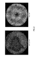
- a type of wafer defect called a slip is depicted in both the amplitude map and the phase map in FIG. 1 .
- the slip has sudden slope changes, it is clearly shown in both the front and the back side of amplitude maps.
- the back surface phase map also has some information related to the slip, the large slope causes the pixel drop out to lose sensitivity and robustness for effective detection of the slip.
- the front surface phase map e.g., the patterned side of phase map
- the slip information disappears due to conventional phase unwrapping errors. Therefore, in such situations, the amplitude maps provide very useful information for feature/defect detection.
- amplitude maps are useful for other types of feature/defect detections as well.
- Amplitude maps are sensitive to any defects where the surface has sudden slope changes and sudden refraction index (n&k) variations.
- n&k sudden refraction index
- FIG. 2 the amplitude map and the phase map generated from the same set of phase-shifted interferograms are shown.
- the amplitude map provides rich wafer information that the phase map does not have.
- the amplitude map can be utilized for detecting defects such as sudden film, slope, material changes and the like on wafer surfaces without departing from the spirit and scope of the present disclosure.
- FIG. 3 is a flow diagram illustrating a method 300 for wafer feature/defect detection utilizing, at least partially, the amplitude maps.
- the measurement system may be calibrated in step 302 .
- the calibration process may calibrate the phase shifting speed and the measurement cavity characteristics of the measurement system.
- the wafer to be measured referred to as the measuring wafer, may then be placed in the cavity in step 304 .
- Two sets of intensity frames that record interferograms on both sides of the wafer may be acquired in step 306 , and a fringe amplitude map may then be extracted from each set of these intensity frames in step 308 .
- the amplitude maps can be used for feature/defect detection in step 310 as previously described.
- the feature/defect detection process as described above is not limited to utilizing only the amplitude maps. That is, phase maps may also be extracted along with the amplitude maps from each set of these intensity frames in step 308 , and the amplitude maps and the phase maps can be used jointly for feature/defect detection in step 310 . It is also contemplated that various detection algorithms, such as local peak and valley, local root mean square, local slope or curvature, filtering, as well many other local surface metrics from other techniques may be utilized without departing from the spirit and scope of the present disclosure.
- the feature/defect detection method as described above is not required to perform feature/defect detection on both surfaces of the wafer. That is, method 300 may be configured to perform feature/defect detection on either or both sides of the wafer without departing from the spirit and scope of the present disclosure.
- FIG. 4 a flow diagram illustrating a method 400 utilizing both amplitude and phase maps of a wafer surface for wafer surface geometry analysis is shown. Steps 402 through 406 have been described above, wherein amplitude maps are generated based on acquired interferograms and used for feature/defect detection.
- the regions identified as being defective in step 404 may be reported and further processed utilizing their corresponding phase maps in order to obtain their height/depth information, as depicted in steps 408 and 410 of FIG. 4 .
- the phase maps can be constructed from acquired video frames with different phase shifts in the measurement system.
- the shape information such as area, length, and orientation of the detected defects can be calculated and reported for defect classification.
- the defect positions are sent to a phase unwrapping module to reconstruct the local surface height profiles in the defect regions in step 410 , from which, the height/depth information of the detected surface defects can be calculated in step 412 and then reported for the defect classification and quantification in step 414 .
- phase unwrapping processes can introduce errors and adversely affect the detection and quantification accuracies. For instance, due to the sharp surface geometry changes in the defect region, conventional phase unwrapping processes often fail to accurately reconstruct the wafer surface height map from the wrapped phase map in the defect regions of several important defects, resulting in many invalid data regions and inaccurate defect shapes, and thus severely affecting the accurate defect detection and quantification. Conventional two-dimensional phase unwrapping processes used for wafer surface reconstruction may also fail to generate satisfying wafer surface height maps on the pattern side, due to the sharp surface topography changes. It is noted, therefore, that the phase unwrapping module utilized in step 410 differs from conventional phase unwrapping processes in several respects and provides several improvements.
- phase unwrapping module utilized in step 410 . More specifically, a local one-dimensional phase unwrapping module, a local two-dimensional phase unwrapping module, as well as an integration technique will be described in details below.
- phase unwrapping techniques can be beneficial because, for many applications of the wafer surface geometry, the exact wafer surface height information is not required, only the local defect height/depth relative to the neighborhood background is needed. Performing phase unwrapping locally will effectively detect and quantify the wafer surface defects, and avoid the serious problems in the whole wafer phase unwrapping, which is only required for obtaining the exact wafer shape information.
- a process referred to as local one-dimensional (1D) phase unwrapping is utilized in step 410 .
- different paths for one-dimensional phase unwrapping can be selected according to the particular detected defect regions from intensity/amplitude maps. For example, if the defect region is a disk shape defect 500 as shown in FIG. 5 , the unwrapping paths can start from the defect centroid and end at the defect boundaries in several major directions 502 and 504 . In another example as shown in FIG. 6 , for a line shaped defect 600 , the one-dimensional phase unwrapping paths 602 can start from one side of the line and end on other side in the orthogonal directions of the line orientation.
- defect height/depth information can be extracted from the acquired phase map and reported as maximum height/depth, mean height/depth, or median height/depth for the defect quantification.
- phase unwrapping process is referred to as local one-dimensional phase unwrapping in the present disclosure because it is performed locally within proximity to each detected defect region, as opposed to a wafer as a whole.
- the phase unwrapping process itself is a one-dimensional process because each phase unwrapping is performed according to a one-dimensional path (as depicted in the examples shown in FIGS. 5 and 6 ). It is contemplated that various one-dimensional phase unwrapping techniques may be utilized to perform each specific unwrapping process, without departing from the spirit and scope of the present disclosure.
- FIG. 7 depicts another example of one-dimensional phase unwrapping.
- This one-dimensional phase unwrapping scheme is suitable for wafer edge region 700 defect detection and quantification.
- surface slope in the radial direction is much higher than in the tangential direction, thus the phase gradient is also much higher in the radial direction.
- the wafer edge region is converted into polar space in different surface sectors, allowing one-dimensional phase unwrapping to be performed locally for each sector.
- FIG. 7 eight major directions are selected to perform the one-dimensional phase unwrapping, and more directions can be used if higher angular characteristic adaption is required. Since the phase map has much lower gradient in the tangential direction, much improved surface reconstruction and defect shape definition in the wafer edge region can be obtained as shown in FIGS. 8-10 . More specifically, FIG. 8 shows a wrapped phase acquired in one wafer edge region, FIG. 9 shows the phase information shown in 8 unwrapped according to a unwrap path, and FIG. 10 shows the unwrapped phase filtered using a high-pass filter. For the slipline detection at the wafer edge region, the acquired phase data segment P(r1:r2, ⁇ 1: ⁇ 2) in the polar space, as shown in FIG.
- Unwrap 1D The unwrap function, Unwrap 1D , here corrects the radian phase angles in the given phase vector P(r, ⁇ 1: ⁇ 2) by adding multiples of ⁇ 2 ⁇ when the absolute jumps between consecutive elements of P(r, ⁇ 1: ⁇ 2) are greater than or equal to the jump tolerance of ⁇ radian. The result is shown in the FIG. 9 .
- the unwrapped, filtered phase can then be used directly for the surface defect detection and quantification, even if the intensity/amplitude maps are not available.
- a process referred to as local two-dimensional (2D) phase unwrapping is utilized in step 410 .
- different local processing area (which may be referred to as a small patch) of the image region can be used to perform the local phase unwrapping and the corresponding different filtering schemes can be used to extract the required surface information.
- an example of local geometry analysis utilizing a 3 ⁇ 3 image patch is used to perform the local two-dimensional phase unwrapping from the center pixel P5. Subsequently, a 3 ⁇ 3 Laplace filter is applied to the unwrapped image patch.
- FIG. 12 shows a cross-shaped image patch used to unwrap the phase from the center pixel P3 and the corresponding 5-pixel high-pass filter is applied on the unwrapped image patch.
- the cross-shaped image patch can be used to unwrapped the phase, and two one-dimensional three-pixel filters can then be used to calculate the local surface slopes in x- and y-directions, respectively.
- phase values of five pixels in the cross-shaped local patch can be expressed as: P ( x,y+ 1) P ( x ⁇ 1, y ) P ( x,y ) P ( x+ 1, y ) P ( x,y ⁇ 1)
- the corresponding local unwrapped cross patch is formed as: P ( x,y+ 1) P ( x ⁇ 1, y ) P ( x,y ) P ( x+ 1, y ) P ( x,y ⁇ 1)
- Unwrap 1D corrects the phase angle difference by adding multiples of ⁇ 2 ⁇ when the absolute phase jumps between these two phase values are greater than or equal to the jump tolerance of ⁇ radian. Then the phase slopes in the X and Y directions can be calculated using these unwrapped phase values as follows:
- this small patch two-dimensional phase unwrapping process is performed for each pixel within a detected defect region to unwrap the two-dimensional phase information for that region. While both these two phase unwrapping operations discussed above are performed only in one direction only for each phase pixel value, for general small patch phase unwrapping, two-dimensional phase unwrapping needs to be carried out to remove the phase jumps in the given local phase patch. It is also contemplated that this small patch two-dimensional phase unwrapping process may be performed for each pixel of the entire wafer image so as to produce an integrated, unwrapped and filtered phase map of the entire wafer.
- Such a process can be very useful for obtaining the geometry images for both bare and patterned wafers, with significant error reduction compared to conventional global phase unwrapping as shown in FIG. 13 .
- This is due to the important fact that any phase unwrapping error in the general two-dimensional phase unwrapping will be accumulated and propagated in the phase unwrapping process, while any phase unwrapping error in the local phase unwrapping will be local and therefore bounded both in location and magnitude.
- FIG. 13 it is clear that global phase unwrapping and filtering of the patterned wafer surface generates a lot of large phase unwrapping errors which limit the wafer geometry application.
- the small patch phase unwrapping and filtering process as described above is also very useful for obtaining local surface slopes for in-plane distortion (IPD) overlay error analysis of bare and patterned wafers. For instance, once the local surface slopes in x- and y-directions are calculated, they can be used to calculate overlay error and provide information for the overlay and leveling error analysis. It is contemplated that the small patch phase unwrapping and filtering process as described above can be used for various other purposes, such as wafer surface nanotopography analysis, overlay error analysis with local slope maps, stress analysis with the local curvature maps and the like without departing from the spirit and scope of the present disclosure. It is also contemplated that the local phase unwrapping methods described above can be used directly in the selected wafer regions to perform the high quality defect detection and quantification, without using the amplitude map.
- IPD in-plane distortion
- amplitude maps can be generated and used to perform defect detection and avoid errors associated with conventional global phase unwrapping.
- amplitude maps themselves cannot provide very useful height and depth information of the detected defects.
- the combined use of amplitude map and local unwrapped map can also allow the better feature/defect detection by using both the feature amplitude and phase maps, since very helpful complementary defect contrast information can be obtained.
- the local phase unwrapping and filtering described above for both one-dimensional and two-dimensional processes can be used directly for high quality detection and quantification of the surface defects, without using the amplitude map. In many applications, such as slipline detection, this method can provide even better results than from the amplitude map because the phase contrast may be greater than the amplitude contrast for such defects. Furthermore, the local phase unwrapping and filtering processes as described above can be used to generate the whole wafer map, reducing errors compared to conventional global phase unwrapping and providing local slope information for pattern overlay analysis, local curvature for surface stress analysis, or general surface shape variation for nanotopography analysis, as well as other applications.
- wafer inspections may include a thin slice of semiconductor material used in the fabrication of integrated circuits and other devices, as well as other thin polished plates such as magnetic disc substrates, gauge blocks and the like.
- the methods disclosed may be implemented as sets of instructions, through a single production device, and/or through multiple production devices. Further, it is understood that the specific order or hierarchy of steps in the methods disclosed are examples of exemplary approaches. Based upon design preferences, it is understood that the specific order or hierarchy of steps in the method can be rearranged while remaining within the scope and spirit of the disclosure.
- the accompanying method claims present elements of the various steps in a sample order, and are not necessarily meant to be limited to the specific order or hierarchy presented.
Landscapes
- Physics & Mathematics (AREA)
- Health & Medical Sciences (AREA)
- Life Sciences & Earth Sciences (AREA)
- Chemical & Material Sciences (AREA)
- Analytical Chemistry (AREA)
- Biochemistry (AREA)
- General Health & Medical Sciences (AREA)
- General Physics & Mathematics (AREA)
- Immunology (AREA)
- Pathology (AREA)
- Testing Or Measuring Of Semiconductors Or The Like (AREA)
- Length Measuring Devices By Optical Means (AREA)
- Investigating Materials By The Use Of Optical Means Adapted For Particular Applications (AREA)
Abstract
Description
I(x,y)=a(x,y)+b(x,y)cos [φ(x,y)]
Where:
Where:
FP(r,θ1:θ2)=
as shown in
P(x,y+1)
P(x−1,y)P(x,y)P(x+1,y)
P(x,y−1)
where Δx and Δy are pixel sizes in x and y directions, respectively.
Claims (25)
Priority Applications (1)
| Application Number | Priority Date | Filing Date | Title |
|---|---|---|---|
| US14/246,895 US9702829B1 (en) | 2013-04-09 | 2014-04-07 | Systems and methods for wafer surface feature detection and quantification |
Applications Claiming Priority (3)
| Application Number | Priority Date | Filing Date | Title |
|---|---|---|---|
| US201361809877P | 2013-04-09 | 2013-04-09 | |
| US201361835437P | 2013-06-14 | 2013-06-14 | |
| US14/246,895 US9702829B1 (en) | 2013-04-09 | 2014-04-07 | Systems and methods for wafer surface feature detection and quantification |
Publications (1)
| Publication Number | Publication Date |
|---|---|
| US9702829B1 true US9702829B1 (en) | 2017-07-11 |
Family
ID=59256983
Family Applications (1)
| Application Number | Title | Priority Date | Filing Date |
|---|---|---|---|
| US14/246,895 Active US9702829B1 (en) | 2013-04-09 | 2014-04-07 | Systems and methods for wafer surface feature detection and quantification |
Country Status (1)
| Country | Link |
|---|---|
| US (1) | US9702829B1 (en) |
Cited By (5)
| Publication number | Priority date | Publication date | Assignee | Title |
|---|---|---|---|---|
| CN109742017A (en) * | 2019-01-25 | 2019-05-10 | 北京半导体专用设备研究所(中国电子科技集团公司第四十五研究所) | Wafer reduction process |
| WO2021141835A1 (en) * | 2020-01-09 | 2021-07-15 | Kla Corporation | Projection and distance segmentation algorithm for wafer defect detection |
| US11238189B2 (en) * | 2014-02-12 | 2022-02-01 | Asml Netherlands B.V. | Process window optimizer |
| TWI872339B (en) * | 2021-06-02 | 2025-02-11 | 美商科磊股份有限公司 | Detection aided two-stage phase unwrapping on pattern wafer geometry measurement |
| CN119850532A (en) * | 2024-12-19 | 2025-04-18 | 广东省大湾区集成电路与系统应用研究院 | Phase unwrapping method, device, equipment, medium and product |
Citations (11)
| Publication number | Priority date | Publication date | Assignee | Title |
|---|---|---|---|---|
| US20030035113A1 (en) * | 2001-08-14 | 2003-02-20 | Jianmin Wang | Quadrature phase shift interferometer with unwrapping of phase |
| US20030155537A1 (en) * | 2001-12-04 | 2003-08-21 | Nova Measuring Instruments Ltd. | Method and system for monitoring a process of material removal from the surface of a patterned structure |
| US20040257587A1 (en) * | 2003-01-28 | 2004-12-23 | Rosakis Ares J. | Full-field optical measurements of surface properties of panels, substrates and wafers |
| US6847458B2 (en) | 2003-03-20 | 2005-01-25 | Phase Shift Technology, Inc. | Method and apparatus for measuring the shape and thickness variation of polished opaque plates |
| US20070146685A1 (en) * | 2005-11-30 | 2007-06-28 | Yoo Woo S | Dynamic wafer stress management system |
| US20090284734A1 (en) * | 2008-05-15 | 2009-11-19 | Kla-Tencor Corporation | Measuring the shape and thickness variation of a wafer with high slopes |
| US7664310B2 (en) | 2000-11-13 | 2010-02-16 | Kla-Tencor Corporation | Advanced phase shift inspection method |
| US7667852B2 (en) | 2007-05-16 | 2010-02-23 | Kla-Tencor Corporation | Measuring the shape, thickness variation, and material inhomogeneity of a wafer |
| US7796273B2 (en) | 2008-11-12 | 2010-09-14 | Zygo Corporation | Phase-shifting interferometry in the presence of vibration |
| US20120177282A1 (en) | 2011-01-07 | 2012-07-12 | Kla-Tencor Corporation | Methods and systems for improved localized feature quantification in surface metrology tools |
| US20140063024A1 (en) * | 2012-12-19 | 2014-03-06 | Iowa State University Research Foundation, Inc. | Three-dimensional range data compression using computer graphics rendering pipeline |
-
2014
- 2014-04-07 US US14/246,895 patent/US9702829B1/en active Active
Patent Citations (12)
| Publication number | Priority date | Publication date | Assignee | Title |
|---|---|---|---|---|
| US7664310B2 (en) | 2000-11-13 | 2010-02-16 | Kla-Tencor Corporation | Advanced phase shift inspection method |
| US20030035113A1 (en) * | 2001-08-14 | 2003-02-20 | Jianmin Wang | Quadrature phase shift interferometer with unwrapping of phase |
| US20030155537A1 (en) * | 2001-12-04 | 2003-08-21 | Nova Measuring Instruments Ltd. | Method and system for monitoring a process of material removal from the surface of a patterned structure |
| US20040257587A1 (en) * | 2003-01-28 | 2004-12-23 | Rosakis Ares J. | Full-field optical measurements of surface properties of panels, substrates and wafers |
| US6847458B2 (en) | 2003-03-20 | 2005-01-25 | Phase Shift Technology, Inc. | Method and apparatus for measuring the shape and thickness variation of polished opaque plates |
| US20070146685A1 (en) * | 2005-11-30 | 2007-06-28 | Yoo Woo S | Dynamic wafer stress management system |
| US7667852B2 (en) | 2007-05-16 | 2010-02-23 | Kla-Tencor Corporation | Measuring the shape, thickness variation, and material inhomogeneity of a wafer |
| US20090284734A1 (en) * | 2008-05-15 | 2009-11-19 | Kla-Tencor Corporation | Measuring the shape and thickness variation of a wafer with high slopes |
| US7796273B2 (en) | 2008-11-12 | 2010-09-14 | Zygo Corporation | Phase-shifting interferometry in the presence of vibration |
| US7796275B2 (en) | 2008-11-12 | 2010-09-14 | Zygo Corporation | Phase-shifting interferometry in the presence of vibration using phase bias |
| US20120177282A1 (en) | 2011-01-07 | 2012-07-12 | Kla-Tencor Corporation | Methods and systems for improved localized feature quantification in surface metrology tools |
| US20140063024A1 (en) * | 2012-12-19 | 2014-03-06 | Iowa State University Research Foundation, Inc. | Three-dimensional range data compression using computer graphics rendering pipeline |
Non-Patent Citations (4)
| Title |
|---|
| Dr. Munther Gdeisat and Dr Francis Lilley, One-Dimensional Phase Unwrapping Problem, Printed online at: http://www.ljmu.ac.uk/GERI/CEORG-Docs/OneDimensionalPhaseUnwrapping-Final.pdf, 11 pages, Print Date Apr. 7, 2014. |
| Dr. Munther Gdeisat and Dr Francis Lilley, One-Dimensional Phase Unwrapping Problem, Printed online at: http://www.ljmu.ac.uk/GERI/CEORG—Docs/OneDimensionalPhaseUnwrapping—Final.pdf, 11 pages, Print Date Apr. 7, 2014. |
| Dr. Munther Gdeisat and Dr Francis Lilley, Two-Dimensional Phase Unwrapping Problem, Printed online at: https://www.ljmu.ac.uk/GERI/CEORG-Docs/Two-Dimensional-Phase-Unwrapping-Final.pdf, 32 pages, Print Date Apr. 7, 2014. |
| Dr. Munther Gdeisat and Dr Francis Lilley, Two-Dimensional Phase Unwrapping Problem, Printed online at: https://www.ljmu.ac.uk/GERI/CEORG—Docs/Two—Dimensional—Phase—Unwrapping—Final.pdf, 32 pages, Print Date Apr. 7, 2014. |
Cited By (12)
| Publication number | Priority date | Publication date | Assignee | Title |
|---|---|---|---|---|
| US11238189B2 (en) * | 2014-02-12 | 2022-02-01 | Asml Netherlands B.V. | Process window optimizer |
| US20220147665A1 (en) * | 2014-02-12 | 2022-05-12 | Asml Netherlands B.V. | Process window optimizer |
| US12141507B2 (en) * | 2014-02-12 | 2024-11-12 | Asml Netherlands B.V. | Process window optimizer |
| CN109742017A (en) * | 2019-01-25 | 2019-05-10 | 北京半导体专用设备研究所(中国电子科技集团公司第四十五研究所) | Wafer reduction process |
| CN109742017B (en) * | 2019-01-25 | 2020-11-13 | 北京半导体专用设备研究所(中国电子科技集团公司第四十五研究所) | Wafer thinning process |
| WO2021141835A1 (en) * | 2020-01-09 | 2021-07-15 | Kla Corporation | Projection and distance segmentation algorithm for wafer defect detection |
| CN114946016A (en) * | 2020-01-09 | 2022-08-26 | 科磊股份有限公司 | Projection and distance cutting algorithm for wafer defect detection |
| US11610296B2 (en) | 2020-01-09 | 2023-03-21 | Kla Corporation | Projection and distance segmentation algorithm for wafer defect detection |
| CN114946016B (en) * | 2020-01-09 | 2024-01-26 | 科磊股份有限公司 | Projection and distance cutting algorithm for wafer defect detection |
| TWI872339B (en) * | 2021-06-02 | 2025-02-11 | 美商科磊股份有限公司 | Detection aided two-stage phase unwrapping on pattern wafer geometry measurement |
| CN119850532A (en) * | 2024-12-19 | 2025-04-18 | 广东省大湾区集成电路与系统应用研究院 | Phase unwrapping method, device, equipment, medium and product |
| CN119850532B (en) * | 2024-12-19 | 2025-09-30 | 广东省大湾区集成电路与系统应用研究院 | Phase unwrapping method, device, equipment, medium and product |
Similar Documents
| Publication | Publication Date | Title |
|---|---|---|
| US10935501B2 (en) | Sub-resolution defect detection | |
| US9255895B2 (en) | Angle-resolved antisymmetric scatterometry | |
| US9702829B1 (en) | Systems and methods for wafer surface feature detection and quantification | |
| CN104520982A (en) | Device-like scatterometry overlay targets | |
| JP2017111147A (en) | Whole wafer inspection method with selectable pixel density | |
| WO2013136620A1 (en) | Phase distribution analysis method and device for fringe image using high-dimensional brightness information, and program therefor | |
| US9632038B2 (en) | Hybrid phase unwrapping systems and methods for patterned wafer measurement | |
| CN106813596A (en) | A kind of self-calibration shadow Moire measuring three-dimensional profile method | |
| CN106767523B (en) | Method and device for improving phase precision | |
| US9019491B2 (en) | Method and apparatus for measuring shape and thickness variation of a wafer | |
| CN105444665B (en) | Location matching method in the measurement of multiple image sensor phase shift interference | |
| US10352691B1 (en) | Systems and methods for wafer structure uniformity monitoring using interferometry wafer geometry tool | |
| CN111121661B (en) | Narrow-band non-monochromatic light n +1 amplitude phase shift test algorithm for smooth surface topography measurement | |
| TWI450053B (en) | Diffraction based overlay linearity testing | |
| US8976337B2 (en) | Method of measuring mark position and measuring apparatus | |
| US9816942B2 (en) | Device and method for inspecting semiconductor materials | |
| US6859566B2 (en) | Method of analyzing fringe image having separate regions | |
| CN117760572A (en) | Dynamic demodulation method of low carrier frequency interference fringes based on two-frame difference and mirror phase shifting | |
| CN108775861A (en) | One kind being based on the dual wavelength time domain phase demodulating method of effective wavelength π/(2k) phase shift | |
| CN108613634B (en) | A method and device for detecting the surface shape of planar components by slope splicing | |
| CN105008903A (en) | Method and device for analyzing the surface of a substrate | |
| US8902429B1 (en) | Focusing detector of an interferometry system | |
| KR102723020B1 (en) | Method and device for examining the surface of an object containing dissimilar materials | |
| CN121297720A (en) | A method for detecting the warpage of VCSEL epitaxial wafers | |
| CN120102592A (en) | A laser damage automatic judgment device and method based on synchronous phase shifting |
Legal Events
| Date | Code | Title | Description |
|---|---|---|---|
| AS | Assignment |
Owner name: KLA-TENCOR CORPORATION, CALIFORNIA Free format text: ASSIGNMENT OF ASSIGNORS INTEREST;ASSIGNORS:CHEN, HAIGUANG;SINHA, JAYDEEP;KAMENSKY, SERGEY;AND OTHERS;SIGNING DATES FROM 20140404 TO 20140430;REEL/FRAME:032852/0200 |
|
| STCF | Information on status: patent grant |
Free format text: PATENTED CASE |
|
| MAFP | Maintenance fee payment |
Free format text: PAYMENT OF MAINTENANCE FEE, 4TH YEAR, LARGE ENTITY (ORIGINAL EVENT CODE: M1551); ENTITY STATUS OF PATENT OWNER: LARGE ENTITY Year of fee payment: 4 |
|
| MAFP | Maintenance fee payment |
Free format text: PAYMENT OF MAINTENANCE FEE, 8TH YEAR, LARGE ENTITY (ORIGINAL EVENT CODE: M1552); ENTITY STATUS OF PATENT OWNER: LARGE ENTITY Year of fee payment: 8 |