EP2284888A2 - Interposer, module and electronics device including the same - Google Patents
Interposer, module and electronics device including the same Download PDFInfo
- Publication number
- EP2284888A2 EP2284888A2 EP20100008048 EP10008048A EP2284888A2 EP 2284888 A2 EP2284888 A2 EP 2284888A2 EP 20100008048 EP20100008048 EP 20100008048 EP 10008048 A EP10008048 A EP 10008048A EP 2284888 A2 EP2284888 A2 EP 2284888A2
- Authority
- EP
- European Patent Office
- Prior art keywords
- substrate
- interposer
- wiring
- semiconductor chip
- module
- Prior art date
- Legal status (The legal status is an assumption and is not a legal conclusion. Google has not performed a legal analysis and makes no representation as to the accuracy of the status listed.)
- Ceased
Links
Images





Classifications
-
- H—ELECTRICITY
- H10—SEMICONDUCTOR DEVICES; ELECTRIC SOLID-STATE DEVICES NOT OTHERWISE PROVIDED FOR
- H10W—GENERIC PACKAGES, INTERCONNECTIONS, CONNECTORS OR OTHER CONSTRUCTIONAL DETAILS OF DEVICES COVERED BY CLASS H10
- H10W44/00—Electrical arrangements for controlling or matching impedance
- H10W44/20—Electrical arrangements for controlling or matching impedance at high-frequency [HF] or radio frequency [RF]
-
- H—ELECTRICITY
- H01—ELECTRIC ELEMENTS
- H01Q—ANTENNAS, i.e. RADIO AERIALS
- H01Q1/00—Details of, or arrangements associated with, antennas
- H01Q1/36—Structural form of radiating elements, e.g. cone, spiral, umbrella; Particular materials used therewith
- H01Q1/38—Structural form of radiating elements, e.g. cone, spiral, umbrella; Particular materials used therewith formed by a conductive layer on an insulating support
-
- H—ELECTRICITY
- H01—ELECTRIC ELEMENTS
- H01Q—ANTENNAS, i.e. RADIO AERIALS
- H01Q19/00—Combinations of primary active antenna elements and units with secondary devices, e.g. with quasi-optical devices, for giving the antenna a desired directional characteristic
- H01Q19/22—Combinations of primary active antenna elements and units with secondary devices, e.g. with quasi-optical devices, for giving the antenna a desired directional characteristic using a secondary device in the form of a single substantially straight conductive element
- H01Q19/24—Combinations of primary active antenna elements and units with secondary devices, e.g. with quasi-optical devices, for giving the antenna a desired directional characteristic using a secondary device in the form of a single substantially straight conductive element the primary active element being centre-fed and substantially straight, e.g. H-antenna
-
- H—ELECTRICITY
- H01—ELECTRIC ELEMENTS
- H01Q—ANTENNAS, i.e. RADIO AERIALS
- H01Q19/00—Combinations of primary active antenna elements and units with secondary devices, e.g. with quasi-optical devices, for giving the antenna a desired directional characteristic
- H01Q19/28—Combinations of primary active antenna elements and units with secondary devices, e.g. with quasi-optical devices, for giving the antenna a desired directional characteristic using a secondary device in the form of two or more substantially straight conductive elements
- H01Q19/30—Combinations of primary active antenna elements and units with secondary devices, e.g. with quasi-optical devices, for giving the antenna a desired directional characteristic using a secondary device in the form of two or more substantially straight conductive elements the primary active element being centre-fed and substantially straight, e.g. Yagi antenna
-
- H—ELECTRICITY
- H05—ELECTRIC TECHNIQUES NOT OTHERWISE PROVIDED FOR
- H05K—PRINTED CIRCUITS; CASINGS OR CONSTRUCTIONAL DETAILS OF ELECTRIC APPARATUS; MANUFACTURE OF ASSEMBLAGES OF ELECTRICAL COMPONENTS
- H05K1/00—Printed circuits
- H05K1/02—Details
- H05K1/14—Structural association of two or more printed circuits
- H05K1/141—One or more single auxiliary printed circuits mounted on a main printed circuit, e.g. modules, adapters
-
- H—ELECTRICITY
- H10—SEMICONDUCTOR DEVICES; ELECTRIC SOLID-STATE DEVICES NOT OTHERWISE PROVIDED FOR
- H10W—GENERIC PACKAGES, INTERCONNECTIONS, CONNECTORS OR OTHER CONSTRUCTIONAL DETAILS OF DEVICES COVERED BY CLASS H10
- H10W44/00—Electrical arrangements for controlling or matching impedance
- H10W44/501—Inductive arrangements
-
- H—ELECTRICITY
- H10—SEMICONDUCTOR DEVICES; ELECTRIC SOLID-STATE DEVICES NOT OTHERWISE PROVIDED FOR
- H10W—GENERIC PACKAGES, INTERCONNECTIONS, CONNECTORS OR OTHER CONSTRUCTIONAL DETAILS OF DEVICES COVERED BY CLASS H10
- H10W70/00—Package substrates; Interposers; Redistribution layers [RDL]
- H10W70/60—Insulating or insulated package substrates; Interposers; Redistribution layers
- H10W70/67—Insulating or insulated package substrates; Interposers; Redistribution layers characterised by their insulating layers or insulating parts
- H10W70/68—Shapes or dispositions thereof
-
- H—ELECTRICITY
- H10—SEMICONDUCTOR DEVICES; ELECTRIC SOLID-STATE DEVICES NOT OTHERWISE PROVIDED FOR
- H10W—GENERIC PACKAGES, INTERCONNECTIONS, CONNECTORS OR OTHER CONSTRUCTIONAL DETAILS OF DEVICES COVERED BY CLASS H10
- H10W70/00—Package substrates; Interposers; Redistribution layers [RDL]
- H10W70/60—Insulating or insulated package substrates; Interposers; Redistribution layers
- H10W70/67—Insulating or insulated package substrates; Interposers; Redistribution layers characterised by their insulating layers or insulating parts
- H10W70/69—Insulating materials thereof
- H10W70/698—Semiconductor materials that are electrically insulating, e.g. undoped silicon
-
- H—ELECTRICITY
- H10—SEMICONDUCTOR DEVICES; ELECTRIC SOLID-STATE DEVICES NOT OTHERWISE PROVIDED FOR
- H10W—GENERIC PACKAGES, INTERCONNECTIONS, CONNECTORS OR OTHER CONSTRUCTIONAL DETAILS OF DEVICES COVERED BY CLASS H10
- H10W72/00—Interconnections or connectors in packages
- H10W72/90—Bond pads, in general
-
- H—ELECTRICITY
- H10—SEMICONDUCTOR DEVICES; ELECTRIC SOLID-STATE DEVICES NOT OTHERWISE PROVIDED FOR
- H10W—GENERIC PACKAGES, INTERCONNECTIONS, CONNECTORS OR OTHER CONSTRUCTIONAL DETAILS OF DEVICES COVERED BY CLASS H10
- H10W90/00—Package configurations
- H10W90/20—Configurations of stacked chips
- H10W90/293—Configurations of stacked chips characterised by non-galvanic coupling between the chips, e.g. capacitive coupling
-
- H—ELECTRICITY
- H05—ELECTRIC TECHNIQUES NOT OTHERWISE PROVIDED FOR
- H05K—PRINTED CIRCUITS; CASINGS OR CONSTRUCTIONAL DETAILS OF ELECTRIC APPARATUS; MANUFACTURE OF ASSEMBLAGES OF ELECTRICAL COMPONENTS
- H05K1/00—Printed circuits
- H05K1/02—Details
- H05K1/0213—Electrical arrangements not otherwise provided for
- H05K1/0237—High frequency adaptations
- H05K1/024—Dielectric details, e.g. changing the dielectric material around a transmission line
-
- H—ELECTRICITY
- H05—ELECTRIC TECHNIQUES NOT OTHERWISE PROVIDED FOR
- H05K—PRINTED CIRCUITS; CASINGS OR CONSTRUCTIONAL DETAILS OF ELECTRIC APPARATUS; MANUFACTURE OF ASSEMBLAGES OF ELECTRICAL COMPONENTS
- H05K1/00—Printed circuits
- H05K1/16—Printed circuits incorporating printed electric components, e.g. printed resistors, capacitors or inductors
-
- H—ELECTRICITY
- H05—ELECTRIC TECHNIQUES NOT OTHERWISE PROVIDED FOR
- H05K—PRINTED CIRCUITS; CASINGS OR CONSTRUCTIONAL DETAILS OF ELECTRIC APPARATUS; MANUFACTURE OF ASSEMBLAGES OF ELECTRICAL COMPONENTS
- H05K2201/00—Indexing scheme relating to printed circuits covered by H05K1/00
- H05K2201/01—Dielectrics
- H05K2201/0183—Dielectric layers
- H05K2201/0191—Dielectric layers wherein the thickness of the dielectric plays an important role
-
- H—ELECTRICITY
- H05—ELECTRIC TECHNIQUES NOT OTHERWISE PROVIDED FOR
- H05K—PRINTED CIRCUITS; CASINGS OR CONSTRUCTIONAL DETAILS OF ELECTRIC APPARATUS; MANUFACTURE OF ASSEMBLAGES OF ELECTRICAL COMPONENTS
- H05K2201/00—Indexing scheme relating to printed circuits covered by H05K1/00
- H05K2201/09—Shape and layout
- H05K2201/09009—Substrate related
- H05K2201/09036—Recesses or grooves in insulating substrate
-
- H—ELECTRICITY
- H05—ELECTRIC TECHNIQUES NOT OTHERWISE PROVIDED FOR
- H05K—PRINTED CIRCUITS; CASINGS OR CONSTRUCTIONAL DETAILS OF ELECTRIC APPARATUS; MANUFACTURE OF ASSEMBLAGES OF ELECTRICAL COMPONENTS
- H05K2201/00—Indexing scheme relating to printed circuits covered by H05K1/00
- H05K2201/10—Details of components or other objects attached to or integrated in a printed circuit board
- H05K2201/10613—Details of electrical connections of non-printed components, e.g. special leads
- H05K2201/10621—Components characterised by their electrical contacts
- H05K2201/10674—Flip chip
-
- H—ELECTRICITY
- H10—SEMICONDUCTOR DEVICES; ELECTRIC SOLID-STATE DEVICES NOT OTHERWISE PROVIDED FOR
- H10W—GENERIC PACKAGES, INTERCONNECTIONS, CONNECTORS OR OTHER CONSTRUCTIONAL DETAILS OF DEVICES COVERED BY CLASS H10
- H10W44/00—Electrical arrangements for controlling or matching impedance
- H10W44/20—Electrical arrangements for controlling or matching impedance at high-frequency [HF] or radio frequency [RF]
- H10W44/203—Electrical connections
- H10W44/209—Vertical interconnections, e.g. vias
-
- H—ELECTRICITY
- H10—SEMICONDUCTOR DEVICES; ELECTRIC SOLID-STATE DEVICES NOT OTHERWISE PROVIDED FOR
- H10W—GENERIC PACKAGES, INTERCONNECTIONS, CONNECTORS OR OTHER CONSTRUCTIONAL DETAILS OF DEVICES COVERED BY CLASS H10
- H10W44/00—Electrical arrangements for controlling or matching impedance
- H10W44/20—Electrical arrangements for controlling or matching impedance at high-frequency [HF] or radio frequency [RF]
- H10W44/203—Electrical connections
- H10W44/216—Waveguides, e.g. strip lines
-
- H—ELECTRICITY
- H10—SEMICONDUCTOR DEVICES; ELECTRIC SOLID-STATE DEVICES NOT OTHERWISE PROVIDED FOR
- H10W—GENERIC PACKAGES, INTERCONNECTIONS, CONNECTORS OR OTHER CONSTRUCTIONAL DETAILS OF DEVICES COVERED BY CLASS H10
- H10W44/00—Electrical arrangements for controlling or matching impedance
- H10W44/20—Electrical arrangements for controlling or matching impedance at high-frequency [HF] or radio frequency [RF]
- H10W44/241—Electrical arrangements for controlling or matching impedance at high-frequency [HF] or radio frequency [RF] for passive devices or passive elements
- H10W44/248—Electrical arrangements for controlling or matching impedance at high-frequency [HF] or radio frequency [RF] for passive devices or passive elements for antennas
-
- H—ELECTRICITY
- H10—SEMICONDUCTOR DEVICES; ELECTRIC SOLID-STATE DEVICES NOT OTHERWISE PROVIDED FOR
- H10W—GENERIC PACKAGES, INTERCONNECTIONS, CONNECTORS OR OTHER CONSTRUCTIONAL DETAILS OF DEVICES COVERED BY CLASS H10
- H10W70/00—Package substrates; Interposers; Redistribution layers [RDL]
- H10W70/60—Insulating or insulated package substrates; Interposers; Redistribution layers
-
- H—ELECTRICITY
- H10—SEMICONDUCTOR DEVICES; ELECTRIC SOLID-STATE DEVICES NOT OTHERWISE PROVIDED FOR
- H10W—GENERIC PACKAGES, INTERCONNECTIONS, CONNECTORS OR OTHER CONSTRUCTIONAL DETAILS OF DEVICES COVERED BY CLASS H10
- H10W72/00—Interconnections or connectors in packages
- H10W72/20—Bump connectors, e.g. solder bumps or copper pillars; Dummy bumps; Thermal bumps
- H10W72/29—Bond pads specially adapted therefor
-
- H—ELECTRICITY
- H10—SEMICONDUCTOR DEVICES; ELECTRIC SOLID-STATE DEVICES NOT OTHERWISE PROVIDED FOR
- H10W—GENERIC PACKAGES, INTERCONNECTIONS, CONNECTORS OR OTHER CONSTRUCTIONAL DETAILS OF DEVICES COVERED BY CLASS H10
- H10W72/00—Interconnections or connectors in packages
- H10W72/50—Bond wires
- H10W72/541—Dispositions of bond wires
- H10W72/5449—Dispositions of bond wires not being orthogonal to a side surface of the chip, e.g. fan-out arrangements
-
- H—ELECTRICITY
- H10—SEMICONDUCTOR DEVICES; ELECTRIC SOLID-STATE DEVICES NOT OTHERWISE PROVIDED FOR
- H10W—GENERIC PACKAGES, INTERCONNECTIONS, CONNECTORS OR OTHER CONSTRUCTIONAL DETAILS OF DEVICES COVERED BY CLASS H10
- H10W72/00—Interconnections or connectors in packages
- H10W72/50—Bond wires
- H10W72/551—Materials of bond wires
- H10W72/552—Materials of bond wires comprising metals or metalloids, e.g. silver
- H10W72/5522—Materials of bond wires comprising metals or metalloids, e.g. silver comprising gold [Au]
-
- H—ELECTRICITY
- H10—SEMICONDUCTOR DEVICES; ELECTRIC SOLID-STATE DEVICES NOT OTHERWISE PROVIDED FOR
- H10W—GENERIC PACKAGES, INTERCONNECTIONS, CONNECTORS OR OTHER CONSTRUCTIONAL DETAILS OF DEVICES COVERED BY CLASS H10
- H10W72/00—Interconnections or connectors in packages
- H10W72/50—Bond wires
- H10W72/551—Materials of bond wires
- H10W72/552—Materials of bond wires comprising metals or metalloids, e.g. silver
- H10W72/5524—Materials of bond wires comprising metals or metalloids, e.g. silver comprising aluminium [Al]
-
- H—ELECTRICITY
- H10—SEMICONDUCTOR DEVICES; ELECTRIC SOLID-STATE DEVICES NOT OTHERWISE PROVIDED FOR
- H10W—GENERIC PACKAGES, INTERCONNECTIONS, CONNECTORS OR OTHER CONSTRUCTIONAL DETAILS OF DEVICES COVERED BY CLASS H10
- H10W72/00—Interconnections or connectors in packages
- H10W72/50—Bond wires
- H10W72/59—Bond pads specially adapted therefor
-
- H—ELECTRICITY
- H10—SEMICONDUCTOR DEVICES; ELECTRIC SOLID-STATE DEVICES NOT OTHERWISE PROVIDED FOR
- H10W—GENERIC PACKAGES, INTERCONNECTIONS, CONNECTORS OR OTHER CONSTRUCTIONAL DETAILS OF DEVICES COVERED BY CLASS H10
- H10W72/00—Interconnections or connectors in packages
- H10W72/90—Bond pads, in general
- H10W72/951—Materials of bond pads
- H10W72/952—Materials of bond pads comprising metals or metalloids, e.g. PbSn, Ag or Cu
-
- H—ELECTRICITY
- H10—SEMICONDUCTOR DEVICES; ELECTRIC SOLID-STATE DEVICES NOT OTHERWISE PROVIDED FOR
- H10W—GENERIC PACKAGES, INTERCONNECTIONS, CONNECTORS OR OTHER CONSTRUCTIONAL DETAILS OF DEVICES COVERED BY CLASS H10
- H10W90/00—Package configurations
- H10W90/701—Package configurations characterised by the relative positions of pads or connectors relative to package parts
- H10W90/721—Package configurations characterised by the relative positions of pads or connectors relative to package parts of bump connectors
- H10W90/724—Package configurations characterised by the relative positions of pads or connectors relative to package parts of bump connectors between a chip and a stacked insulating package substrate, interposer or RDL
-
- H—ELECTRICITY
- H10—SEMICONDUCTOR DEVICES; ELECTRIC SOLID-STATE DEVICES NOT OTHERWISE PROVIDED FOR
- H10W—GENERIC PACKAGES, INTERCONNECTIONS, CONNECTORS OR OTHER CONSTRUCTIONAL DETAILS OF DEVICES COVERED BY CLASS H10
- H10W90/00—Package configurations
- H10W90/701—Package configurations characterised by the relative positions of pads or connectors relative to package parts
- H10W90/751—Package configurations characterised by the relative positions of pads or connectors relative to package parts of bond wires
- H10W90/754—Package configurations characterised by the relative positions of pads or connectors relative to package parts of bond wires between a chip and a stacked insulating package substrate, interposer or RDL
Definitions
- the present invention relates to an interposer for intermediating electric connection and mechanical connection among a plurality of electronic devices with each wiring rule different from each other, a module, and an electronics device including the same.
- a single-digit or more gap between a pad pitch of a semiconductor chip whose miniaturization has been rapidly improved and a pad pitch of a substrate (mount substrate) on which the semiconductor chip is mounted.
- a gap leads to difficulty to reflect high performance obtained by progress of semiconductor technology and performance of a high function chip to a device or a system.
- the practically used pad pitch of the semiconductor chip has been improved to 50 ⁇ m or less, while the pad pitch of the mount substrate (for example, a Print Circuit Board (PCB)) is about 500 ⁇ m. It is expected that miniaturization of the pad pitch of the semiconductor chip will be improved according to scaling rule in the future. Meanwhile, miniaturization of the pad pitch of the PCB may be improved relatively slowly.
- PCB Print Circuit Board
- a signal line As the carrier frequency is increased, influence of the length becomes increased.
- a carrier of a digital circuit a signal with 400 MHz class clock frequency is used.
- high frequency band (from GHz to millimeter waveband) is used.
- High frequency has a short wavelength.
- half-wavelength of 60 GHz is 2.5 mm in vacuum and 1.2 mm on the PCB.
- the physical length of a certain signal line is equal to or more than half of the electric length of a carrier frequency, problematic signal resonance phenomenon is shown in the signal line.
- the silicon interposer according to Japanese Unexamined Patent Application Publication No. 2008-42904 is composed of a wiring for converting a wiring pitch (including a TSV (Through Silicon Via)) and a cavity (concave section) for the after-mentioned antenna part.
- the silicon interposer has a structure in which on an interposer substrate, an antenna pattern formed in another silicon substrate (upper silicon section) is integrated. Thereby, the connecting distance from a semiconductor chip as a high frequency analog circuit is decreased, and the signal quality is able to be improved.
- an interposer including a substrate having a front face and a rear face, a wiring that is formed on the front face side of the substrate and is electrically connected to a semiconductor chip, an electric device connected to the wiring, and a concave section that is formed from the rear face side of the substrate in a position corresponding to the electric device.
- concave section includes a penetrating shape obtained by totally removing the substrate at the bottom part of the concave section, in addition to a shape in which the substrate remains at the bottom part of the concave section.
- concave section that is formed from the rear face side of the substrate in a position corresponding to the electric device means a state that the concave section is in a position above which at least part of the electric device provided on the substrate is provided.
- a module including the interposer of the foregoing embodiment of the invention and a semiconductor chip mounted on the interposer
- an electronics device including the interposer of the foregoing embodiment of the invention, a semiconductor chip mounted on the interposer, and a mount substrate on which the interposer is mounted.
- the wiring and the electric device are previously provided on the substrate. Thereby, joint between the substrate and the wiring, patterning of the electric device such as an antenna and the semiconductor chip and the like are not necessitated. Accordingly, the manufacturing steps are simplified.
- the wiring and the electric device are provided on the substrate.
- the manufacturing steps are simplified. Thereby, reliability and yield ratio are able to be improved.
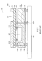
- FIG. 1 is a cross sectional view of a module according to an embodiment of the invention.
- FIG. 2 is a planar view of the module illustrated in FIG. 1 .
- FIG. 3 is a cross sectional view illustrating a module of another example.
- FIGs. 4A and 4B are characteristics diagrams of radio emission of the module illustrated in FIG. 1 .
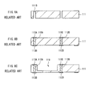
- FIGs. 5A to 5C are views illustrating a method of manufacturing the module illustrated in FIG. 1 in order of steps.
- FIGs. 6A to 6C are views illustrating steps following FIGs. 5A to 5C .
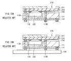
- FIG. 7 is a cross sectional view of a module according to a comparative example.
- FIGs. 8A to 8C are views illustrating a method of manufacturing the module illustrated in FIG. 7 in order of steps.
- FIGs. 9A to 9C are views illustrating steps following FIGs. 8A to 8C .
- FIGs. 10A to 10B are views illustrating steps following FIGs. 9A to 9C .
- FIG. 11 is a cross sectional view of a module according to a modified example.
- FIG. 12 illustrates a planar view of the module illustrated in FIG. 11 .
- FIG. 13 is a cross sectional view illustrating a module of another example.
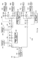
- FIG. 14 is a functional block diagram of an electronics device according to an application example of the module.
- FIG. 1 illustrates a cross sectional structure of a module 1A including an interposer 10A and a semiconductor chip 20 according to an embodiment of the invention.
- FIG. 2 illustrates a planar structure thereof.
- FIG. 1 is a cross sectional structure taken along line I-I of FIG. 2 .
- a dielectric layer 14 is formed on a substrate 11 including a concave section 19A.
- a wiring layer 16 and an electric device 17 (in this case, an antenna) are provided above the dielectric layer 14, the semiconductor chip 20 connected to a wiring layer 16 is provided.
- the interposer 10A connects the semiconductor chip 20 to a mount substrate 30 (in this case, a printed board) with a penetrating electrode 12 provided in the substrate 11 in between.
- a silicon (Si) substrate or a silicon carbide (SiC) substrate having a thickness from 50 to 400 ⁇ m both inclusive is desirably used to match with a material of the semiconductor chip 20 described later.
- a material of the substrate 11 is not limited thereto, but other semiconductor material or a dielectric material may be used. Examples of other semiconductor materials include SiGe and GaAs. Examples of dielectric materials include ceramic, glass (for example, Pyrex, SD2, and quartz), a resin (glass epoxy and BT resin), and an organic polymer.
- the substrate 11 is provided with the concave section 19A having a pit on the rear face side of the substrate 11 in a position corresponding to at least part of the antenna 17 provided in the dielectric layer 14.
- the concave section 19A is desirably formed in a position opposed to the antenna 17 described later, that is, is desirably formed to cover the entire antenna 17 in the overhead view as illustrated in FIG. 2 .
- the substrate 11 remains at the bottom part of the concave section 19A.
- the substrate 11 does not necessarily remain at the bottom part of the concave section 19A, but a penetrating aperture 19B formed by totally removing the substrate 11 may be adopted as illustrated in FIG. 3 .
- the substrate 11 is not totally removed, but part thereof remains.
- the concave section 19A may be formed in a palisade state or in a lattice pattern.
- the planar pattern of the concave section 19A (aperture 19B) is, for example, circular or rectangle.
- the planar pattern of the concave section 19A (aperture 19B) is not limited thereto, but is determined by relation with the shape and the size of an electric device arranged above the concave section 19A (aperture 19B).
- the substrate 11 includes the penetrating electrode 12 having a diameter of 50 ⁇ m, for example.
- the penetrating electrode 12 is formed from, for example, copper (Cu).
- Pads 13A and 13B are provided above and below the penetrating electrode 12.
- An insulating layer 11A is provided between the substrate 11 and the dielectric layer 14.
- a silicon nitride film (SiN) having a thickness, for example, from 0.01 to 0.3 ⁇ m both inclusive is formed on a silicon oxide film (SiO 2 ) having a thickness, for example, from 0.01 to 4 ⁇ m both inclusive.
- the insulting layer 11A functions as an etching stopper layer in providing the concave section 19A (aperture 19B) in the substrate 11.
- the insulating layer 11A is dispensable as a structure for attaining performance of a so-called membrane device having the concave section 19A (aperture 19B) such as the interposer 10A of this embodiment.
- the dielectric layer 14 is formed from a low dielectric constant material with small loss for a high frequency signal such as benzocyclobutene (BCB).
- the thickness of the dielectric layer 14 is determined by both electric characteristics and mechanical strength, and is, for example, from 1 ⁇ m to 20 ⁇ m both inclusive.
- an optimal film thickness of the dielectric layer 14 varies according to the wiring layout rule.
- the film thickness range is determined by viewpoint of wiring impedance matching. Specifically, for example, in the case of 50 ⁇ matching under the condition of wiring of 60 GHz, high frequency wiring with line/space of 50 ⁇ m/50 ⁇ m, and micro strip line, a film thickness of 20 ⁇ m is necessitated.
- the dielectric layer 14 is desirably manufactured by technique of forming a BCB film including a thin film of several ⁇ m or less to a thick film of several ten ⁇ m and a multilayer film technique.
- the dielectric layer 14 other material out of the generally used dielectric materials is able to be used, as long as such a material has small loss for a high frequency signal and has a strength to the degree with which a bridge structure is able to be retained even if the concave section 19A (aperture 19B) is provided in the substrate 11 as described above.
- a material has small loss for a high frequency signal and has a strength to the degree with which a bridge structure is able to be retained even if the concave section 19A (aperture 19B) is provided in the substrate 11 as described above.
- an inorganic material such as SiO 2
- diamond-like carbon (DLC) is able to be used.
- the wiring layer 16 and the antenna 17 are provided.
- the wiring layer 16 is composed of a combination of at least one or more multilayer wiring layers (in this case, one layer: wirings 16A and 16B) and an interlayer connection wiring layer (via contact 15A).
- the wiring layer 16 is made of a conductive material, for example, a metal material such as Al (aluminum) and AlCu (aluminum copper).
- the antenna 17 is an artificial Yagi antenna made of an Al wiring. It is needless to say that the device is not limited thereto, but other passive device such as a patch antenna and a slot antenna may be used. Further, a metal material other than Al may be used.
- the antenna 17 and the after-mentioned semiconductor chip 20 are desirably arranged in the proximity of each other.
- accumulated loss of the transmitting and receiving circuit is able to be decreased.
- a gold (Au) wire being about 1.5 mm long having a diameter of 20 ⁇ m has 0.8 nH parasitic inductance, and signal loss of about 1 dB is generated in 60GHz.
- the antenna 17 and the semiconductor chip 20 are arranged as in this embodiment, the distance between the antenna 17 and the semiconductor chip 20 becomes 200 ⁇ m, and signal loss is largely decreased down to 0.1 dB.
- the interlayer connection wiring layer is obtained by forming a through hole 14a in the dielectric layer 14A and filling the through hole 14a with a metal material.
- the form of the interlayer connection wiring layer is not limited thereto, and any shape is able to be adopted as long as wiring in different layers are connected to each other.
- FIG. 4A illustrates characteristics of reflectance characteristics (S11) of an artistic Yagi antenna with central frequency of 60 GHz.
- FIG. 4B illustrates calculation result of radio emission characteristics of far field (three dimensional illustration).
- the calculation result of the antenna gain of the membrane antenna is -5dBi, while the calculation result of the reference antenna that is not the membrane antenna is -10dBi. Accordingly, a high antenna gain is able to be obtained by providing the concave section 19A (aperture 19B) in a position opposed to the antenna 17 as in this embodiment.
- the semiconductor chip 20 is RFIC.
- the semiconductor chip 20 is a device that up-converts a signal in several hundred MHz band inputted from, for example, a base band chip to a signal in high frequency band as a signal in milliwave band, for example.
- the semiconductor chip 20 is connected to the wirings 16A and 16B with pads 21A and 21B and solder layers 22A and 22B in between.
- the wiring 16A is connected to the penetrating electrode 12 with the via 15A and the pad 13A in between. Meanwhile, the wiring 16B is connected to the antenna 17.
- the printed board 30 is a mount substrate on which many electronic parts such as a resistor and a condenser in addition to the module 1A (1B) are mounted, and configures an electronic circuit by connecting these electronic parts to each other by wiring.
- the module 1A (1B) may be manufactured, for example, by the method illustrated in FIGs. 5A to 5C and FIGs. 6A to 6C .
- the insulating layer 11A is formed. Specifically, an etching mask is patterned on the front face of the substrate 11 having a thickness of, for example, 400 ⁇ m. Next, the substrate 11 is etched in the thickness direction under vacuum condition by using a DRIE (Deep Reactive Ion Etching) apparatus to form the through hole 11B. Subsequently, the substrate 11 is heated at, for example, 1000 deg C to form an SiO 2 film having a thickness of 3 ⁇ m by thermal oxidation under water vapor atmosphere.
- DRIE Deep Reactive Ion Etching
- a SiN film having a thickness from 0.1 to 0.3 ⁇ m both inclusive is formed by, for example, CVD (Chemical Vapor Deposition) method to obtain the insulating film 11A.
- the penetrating electrode 12 is formed as illustrated in FIG. 5B .
- a seed layer (not illustrated)
- base titanium (Ti) having a thickness of, for example, 50 nm
- copper (Cu) thin film having a thickness of, for example, 300 nm were formed by, for example, PVD (Physical Vapor Deposition).
- PVD Physical Vapor Deposition
- CMP Chemical Mechanical Polishing
- an AlCu thin film having, for example, a diameter of 100 ⁇ m and a thickness of 100 nm is formed by, for example, photolithography and dry etching such as DRIE.
- the dielectric layer 14A, the via contact 15A, the wirings 16A and 16B, and the antenna 17 are formed. Specifically, first, on the top face of the substrate 11, the dielectric layer 14A is formed by spin coat method with the use of BCB as a low dielectric constant material. The through hole 14a that reaches the pad 13A is formed in the dielectric layer 14A. After that, the through hole 14a is filled with AlCu to form the via contact 15A. Next, on the dielectric layer 14A, the wirings 16A and 16B and the antenna 17 are formed by photolithography and dry etching. Next, by using a similar method, a dielectric layer 14C, via contacts 15B and 15C, and pads 16C and 16D are formed on the bottom face of the substrate 11.
- apertures 18A and 18B for connecting the semiconductor chip 20 with the wirings 16A and 16B are formed.
- the dielectric layer 14C is formed on the top face of the substrate 11 by spin coat method by using, for example, BCB
- the dielectric layer 14C in a region on which the semiconductor chip 20 is mounted is removed by photolithography and dry etching.
- a hard mask is formed on the bottom face of the substrate 11.
- the substrate 11 is etched by, for example, DRIE to form the concave section 19A (aperture 19B) and complete the interposer 10A having a desired membrane structure.
- etching conditions vertical process by SF 6 /C 4 H 8 known as Bosch process or dry process by XeF 2 is used. Further, wet process using tetramethylammonium hydroxide (TMAH) or potassium hydroxide (KOH) may be used.
- TMAH tetramethylammonium hydroxide
- KOH potassium hydroxide
- the semiconductor chip 20 is mounted on the top face of the interposer 10A.
- the pads 21A and 21B provided on the bottom face of the semiconductor chip 20 are thermally compression-bonded with the top face of the interposer 10A, for example, at 150 deg C and 100 kPa. Accordingly, joint between the semiconductor chip 20 and the interposer 10A is completed.
- the pads 16C and 16D of the interposer 10A are connected with pads 31A and 31B formed on the printed board 30 with bumps 32A and 32B in between, and the interposer 10A on which the semiconductor chip 20 is provided is mounted on the printed board 30. Thereby, the module 1A is completed.
- the dielectric layer 14 is formed on the substrate 11, and the wiring layer 16 and the antenna 17 are included in the dielectric layer 14. Further, the penetrating electrode 12 is provided in the substrate 11.
- the interposer 10A connects the printed board 30 and the semiconductor chip 20 provided on the interposer 10A with the penetrating electrode 12 in between. As described above, by using the interposer 10A, the semiconductor chip 20 and the printed board 30 with each wiring pitch different from each other are able to be relayed electrically and mechanically.
- the concave section 19A (aperture 19B) formed from the rear face side of the substrate 11 is provided. Thereby, parasitic capacity and eddy current between the substrate 11 and the antenna 17 are inhibited.
- the semiconductor chip 20 and the printed board 30 are connected based on a narrow wiring pitch in the connection section on the semiconductor chip 20 side and based on a wide wiring pitch in the connection section on the printed board 30 side.
- the pads composing the connection section and wirings for their connection are the wiring layer 16 provided in the dielectric layer 14 on the substrate 11 of the interposer 10A, the penetrating electrode 12, and the wiring layer 16 (the pads 13B and 16C and the via contact 15B) on the rear face side of the substrate 11.
- Their lines and spaces are formed by using a processing means of the semiconductor chip.
- processing is made by a single-digit or more refined processing technology or based on a rule equal to a wiring processing rule of semiconductor chips.
- the wiring layer 16 (the pads 13C and 16D and the via contact 15C) on the right side of the rear face side of the substrate 11 of the interposer 10A (10B) in FIG. 1 ( FIG. 3 ) is a dummy connection layer for achieving the mechanical balance in mounting on the printed board 30 or a GND (ground) connection layer of the substrate 11.
- FIG. 7 illustrates a cross sectional structure of an existing module 100 according to a comparative example.
- a second Si substrate 211 that has a wiring 216A and an antenna 217 on the bottom face and has a semiconductor chip (integrated circuit chip) 220 is jointed to a first Si substrate (interposer) 111 that has a concave section 119 by a joint metal.
- the concave section 119 is intended to contain the semiconductor chip 220.
- FIG. 8A the manufacturing steps illustrated in FIGs. 8A to 8C , FIGs. 9A to 9C , and FIGs. 10A to 10B may be used. Each step thereof will be hereinafter described in short.
- the first Si substrate 111 is processed to form a through hole 111B. After that, an insulating film (not illustrated) is formed.
- FIG. 8B after a penetrating electrode 112A is formed, pads 113A, 113B, 113C, and 113D are formed.
- FIG. 8C the concave section 119 is formed, and the first Si substrate 111 to become the interposer is formed.
- a dielectric layer 214 including wiring 216A and 216B and the antenna 217 is formed on the second Si substrate 211.
- the second Si substrate 211 is processed into a thin film by CMP.
- a concave section 219 is provided in the second Si substrate 211 to obtain a membrane structure.
- the semiconductor chip 220 is connected, and the second Si substrate 211 on which the semiconductor chip 220 is provided is formed.
- the first Si substrate 111 and the second Si substrate 211 are jointed by thermal compression bonding.
- the resultant is mounted on a printed board 130 by using solder to complete the module 100.
- penetrating electrodes 112A and 112B of the first Si substrate 111 are jointed to the wiring layer 216 provided on the bottom face of the second Si substrate 211. Since alignment precision of the joint step is low, it leads to restriction of miniaturization. In addition, in the case where transmission frequency is high, signal loss due to wiring mismatch or the like is shown. Further, wiring step for jointing the first Si substrate 111 to the second Si substrate 211 is necessitated. As described above, the manufacturing steps become complicated.
- the interposer 10A (10B) of this embodiment since the wiring layer 16 is provided in the dielectric layer 14 that is directly formed on the substrate 11, the foregoing steps are not necessitated. Thus, the manufacturing steps are able to be simplified.
- the dielectric layer 14 is formed on the substrate 11, and the wiring layer 16 and the antenna 17 are provide in the dielectric layer 14.
- the wiring area is able to be reduced. That is, the size of the module 1A (1B) is able to be decreased. Further, by using the penetrating electrode 12, other module is able to be layered on the module 1A (1B).
- the concave section 19A (or the aperture 19B penetrating the substrate 11) is provided on the rear face side of the substrate 11 in a position corresponding to at least part of the antenna 17.
- parasitic capacity and eddy current between the substrate and the device are inhibited. Accordingly, signal loss is able to be inhibited.
- FIG. 11 illustrates a cross sectional structure of the module 2A including the interposer 10C having the concave section 19A in the substrate 11
- FIG. 12 illustrates a planar structure thereof
- FIG. 13 illustrates a cross sectional structure of the module 2B including the interposer 10D having the aperture 19B in the substrate 11.
- FIG. 11 and FIG. 13 are a cross sectional structure taken along line II-II of FIG. 12 .
- the same referential symbols are affixed thereto and the descriptions thereof will be omitted.
- the interposer 10C (10D) connects the wiring layer 16 to the printed board 30 with a wiring 33.
- a chip-use connection section 23 is provided together with a wire pad for wire connection with the printed board 30 and a decoupling condenser (MIM capacitor) (not illustrated) for removing wiring noise is provided, in addition to the dielectric layer 14 in which the wiring layer 16 and the electric device 17 described in the foregoing embodiment are formed.
- MIM capacitor decoupling condenser
- the wiring layer 16 and the printed board 30 are connected by the wiring 33.
- the module 2A (2B) is able to be freely arranged on the printed board 30 in addition to the effect of the foregoing embodiment.
- the number of pins is small and device occupied area difference is smaller than in a BGA (Ball Grid Array) or the like, it is more inexpensive to adopt wiring by the wire 33 than manufacturing the penetrating electrode 12.
- the cost is able to be reduced.
- FIG. 14 illustrates a block configuration of the communication apparatus as an electronics device.
- Examples of the communication apparatus illustrated in FIG. 14 include a mobile phone, a personal digital assistant (PDA), and a wireless LAN apparatus.
- the communication apparatus includes a transmission circuit 300A (module), a receiving circuit 300B (module), a transmitting/receiving switch 301 for switching the transmitting/receiving route, a high frequency filter 302, and a transmitting/receiving antenna 303.
- the transmission circuit 300A includes two digital/analog converters (DAC) 311I and 311 Q, and two bandpass filters 312I and 312Q that respectively correspond to transmission data of I channel and transmission data of Q channel, a modulator 320, a transmission PLL (Phase-Locked Loop) circuit 313, and a power amplifier 314.
- the modulator 320 includes two buffer amplifiers 321I and 321Q and two mixers 322I and 322Q that respectively correspond to the foregoing two bandpass filters 312I and 312Q, a phase module 323, an adder 324, and a buffer amplifier 325.
- the receiving circuit 300B includes a high frequency section 330, a bandpass filter 341, a channel selection PLL circuit 342, an intermediate frequency circuit 350, a bandpass filter 343, a demodulator 360, an intermediate frequency PLL circuit 344, two bandpass filters 345I and 345Q and two analog/digital converters (ADC) 346I and 346Q that respectively correspond to receiving data of I channel and receiving data of Q channel.
- the high frequency section 330 includes a low noise amplifier 331, buffer amplifiers 332 and 334, and a mixer 333.
- the intermediate frequency circuit 350 includes buffer amplifiers 351 and 353 and an Auto Gain Controller (AGC) circuit 352.
- the modulator 360 includes a buffer amplifier 361, two mixers 362I and 362Q and two buffer amplifiers 363I and 363Q that respectively correspond to the foregoing two bandpass filters 345I and 345Q, and a phase module 364.
- each transmission data is processed in the following procedure. That is, first, the transmission data is converted to an analog signal in the DAC 311I and 311Q. Subsequently, signal components other than the band of the transmission signal are removed in the bandpass filters 312I and 312Q, and then the resultant signal is supplied to the modulator 320. Subsequently, in the modulator 320, the signal is supplied to the mixers 322I and 322Q via the buffer amplifiers 321I and 321Q, the resultant signal is mixed with a frequency signal corresponding to the transmission frequency supplied from the transmission PLL circuit 313, and then modulated.
- both mixed signals are added in the adder 324, and thereby one system transmission signal is obtained.
- the signal phase is shifted 90 degrees in the phase module 323.
- the I channel signal and the Q channel signal are modulated orthogonal to each other.
- the signal is supplied to the power amplifier 314 via the buffer amplifier 325.
- the signal is amplified to obtain a given transmission power.
- the signal amplified in the power amplifier 314 is supplied to the antenna 303 via the transmitting/receiving switch 301 and the high frequency filter 302, and thereby is wireless-transmitted via the antenna 303.
- the high frequency filter 302 functions as a bandpass filter for removing signal components other than the frequency band out of a transmitted or received signal in the communication apparatus.
- the signal is processed in the following procedure. That is, first, in the high frequency section 330, the received signal is amplified in the low noise amplifier 331. Subsequently, signal components other than the receiving frequency band are removed by the bandpass filter 341. After that, the signal is supplied to the mixer 333 via the buffer amplifier 332. Subsequently, the signal is mixed with a frequency signal supplied from the channel selection PPL circuit 342, and a given transmission channel signal is set as an intermediate frequency signal. Thereby, the signal is supplied to the intermediate frequency circuit 350 via the buffer amplifier 334.
- the signal is supplied to the bandpass filter 343 via the buffer amplifier 351. Thereby, signal components other than the band of the intermediate frequency signal are removed.
- the resultant signal subsequently becomes an almost constant gain signal in the AGC circuit 352.
- the signal is supplied to the demodulator 360 via the buffer amplifier 353.
- the signal is supplied to the mixers 362I and 362Q via the buffer amplifier 361.
- the signal is mixed with a frequency signal supplied from the intermediate frequency PPL circuit 344.
- the I channel signal component and the Q channel signal component are demodulated.
- the signal phase is shifted 90 degrees in the phase module 364.
- the I channel signal component and the Q channel signal component that are modulated perpendicular to each other are demodulated.
- the I channel signal and the Q channel signal are supplied to the bandpass filters 345I and 345Q, respectively, and thereby signal components other than the I channel signal and the Q channel signal are removed.
- the signal is supplied to the ADC 346I and 346Q to obtain digital data. Thereby, I channel receiving data and Q channel receiving data are obtained.
- the interposers 10A to 10D described in the foregoing embodiment and the foregoing modified example are applied to connect the antenna 303, the high frequency filter 302, the bandpass filters 341 and 343, the modulator 320, and the demodulator 360 to the mount substrate.
- the interposers 10A to 10D described in the foregoing embodiment and the foregoing modified example are applied to connect the antenna 303, the high frequency filter 302, the bandpass filters 341 and 343, the modulator 320, and the demodulator 360 to the mount substrate.
- the interposers 10A to 10D described in the foregoing embodiment and the foregoing modified example are applied to the connection between the foregoing respective elements and the mount substrate.
- application is not always limited thereto.
- the interposers 10A to 10D may be applied to the wiring connection in an integrated device composed of a CMOS device and an MEMS sensor with each miniaturization different from each other. In this case, effect similar to the foregoing effect is able to be obtained as well. Further, the interposers 10A to 10D are able to be applied to the integration of an analog circuit device and a digital circuit device.
- the penetrating electrode 12 is used for connecting the semiconductor chip 20 to the printer substrate 30.
- connection is made by a through-hole wiring, similar effect is obtained.
- the antenna 17 is used as an electric device (passive device).
- the device is not limited thereto, but an inductor or a coupler may be used.
- an electric device other than the passive device such as a high frequency switch and a varicap diode used as a coupling condenser of a high frequency transmission line, or a filter or a variable filter combined with an electric device may be used.
Landscapes
- Engineering & Computer Science (AREA)
- Microelectronics & Electronic Packaging (AREA)
- Variable-Direction Aerials And Aerial Arrays (AREA)
- Internal Circuitry In Semiconductor Integrated Circuit Devices (AREA)
- Structures For Mounting Electric Components On Printed Circuit Boards (AREA)
Abstract
Description
- 1. Field of the Invention
- The present invention relates to an interposer for intermediating electric connection and mechanical connection among a plurality of electronic devices with each wiring rule different from each other, a module, and an electronics device including the same.
- 2. Description of the Related Art
- There is a single-digit or more gap between a pad pitch of a semiconductor chip whose miniaturization has been rapidly improved and a pad pitch of a substrate (mount substrate) on which the semiconductor chip is mounted. Such a gap leads to difficulty to reflect high performance obtained by progress of semiconductor technology and performance of a high function chip to a device or a system. For example, the practically used pad pitch of the semiconductor chip has been improved to 50 µm or less, while the pad pitch of the mount substrate (for example, a Print Circuit Board (PCB)) is about 500 µm. It is expected that miniaturization of the pad pitch of the semiconductor chip will be improved according to scaling rule in the future. Meanwhile, miniaturization of the pad pitch of the PCB may be improved relatively slowly.
- In the past, as a means for compensating the pad pitch gap and electrically and mechanically bonding the semiconductor chip with the mount substrate, wiring made of gold (Au) or aluminum (Al) has been used. Specifically, the semiconductor chip is die-bonded (mechanically connected) onto an organic substrate having 500 µm class wiring rule, and wiring pads of the organic substrate and the semiconductor chip are wire-connected (electrically connected).
- In a signal line, as the carrier frequency is increased, influence of the length becomes increased. For a carrier of a digital circuit, a signal with 400 MHz class clock frequency is used. Meanwhile, for a carrier of a transmitting and receiving circuit, high frequency band (from GHz to millimeter waveband) is used. High frequency has a short wavelength. For example, half-wavelength of 60 GHz is 2.5 mm in vacuum and 1.2 mm on the PCB. In the case where the physical length of a certain signal line is equal to or more than half of the electric length of a carrier frequency, problematic signal resonance phenomenon is shown in the signal line. Thus, in view of securing signal quality, it is desirable that layout is made so that the length of the signal line is smaller than the half of the electric length of the transmission carrier signal. Accordingly, in recent years, a packaging smaller than that of a mounting mode with the use of a wire becomes available. A silicon interposer with which power loss reduction and improved signal quality by short wiring are expected attracts attention, and the technical development thereof has been actively made (for example, Japanese Unexamined Patent Application Publication No.
2008-42904 - The silicon interposer according to Japanese Unexamined Patent Application Publication No.
2008-42904 - However, in the interposer exemplified as above, there has been a disadvantage that its manufacturing steps such as jointing the silicon substrate provided with the antenna pattern and patterning the antenna section and the semiconductor chip section become complicated, and thus reliability and yield ratio are lowered.
- In view of the foregoing disadvantage, in the invention, it is desirable to provide an interposer with which the manufacturing steps are able to be simplified, a module, and an electronics device including the same.
- According to an embodiment of the invention, there is provided an interposer including a substrate having a front face and a rear face, a wiring that is formed on the front face side of the substrate and is electrically connected to a semiconductor chip, an electric device connected to the wiring, and a concave section that is formed from the rear face side of the substrate in a position corresponding to the electric device.
- In this case, "concave section" includes a penetrating shape obtained by totally removing the substrate at the bottom part of the concave section, in addition to a shape in which the substrate remains at the bottom part of the concave section.
Further, "concave section that is formed from the rear face side of the substrate in a position corresponding to the electric device" means a state that the concave section is in a position above which at least part of the electric device provided on the substrate is provided. - According to an embodiment of the invention, there is provided a module including the interposer of the foregoing embodiment of the invention and a semiconductor chip mounted on the interposer
- According to an embodiment of the invention, there is provided an electronics device including the interposer of the foregoing embodiment of the invention, a semiconductor chip mounted on the interposer, and a mount substrate on which the interposer is mounted.
- In the interposer, the module, and the electronics device including the same of the embodiment of the invention, the wiring and the electric device are previously provided on the substrate. Thereby, joint between the substrate and the wiring, patterning of the electric device such as an antenna and the semiconductor chip and the like are not necessitated. Accordingly, the manufacturing steps are simplified.
- In the interposer, the module, and the electronics device including the same of the embodiment of the invention, the wiring and the electric device are provided on the substrate. Thus, the manufacturing steps are simplified. Thereby, reliability and yield ratio are able to be improved.
- Other and further objects, features and advantages of the invention will appear more fully from the following description.
-
FIG. 1 is a cross sectional view of a module according to an embodiment of the invention. -
FIG. 2 is a planar view of the module illustrated inFIG. 1 . -
FIG. 3 is a cross sectional view illustrating a module of another example. -
FIGs. 4A and 4B are characteristics diagrams of radio emission of the module illustrated inFIG. 1 . -
FIGs. 5A to 5C are views illustrating a method of manufacturing the module illustrated inFIG. 1 in order of steps. -
FIGs. 6A to 6C are views illustrating steps followingFIGs. 5A to 5C . -
FIG. 7 is a cross sectional view of a module according to a comparative example. -
FIGs. 8A to 8C are views illustrating a method of manufacturing the module illustrated inFIG. 7 in order of steps. -
FIGs. 9A to 9C are views illustrating steps followingFIGs. 8A to 8C . -
FIGs. 10A to 10B are views illustrating steps followingFIGs. 9A to 9C . -
FIG. 11 is a cross sectional view of a module according to a modified example. -
FIG. 12 illustrates a planar view of the module illustrated inFIG. 11 . -
FIG. 13 is a cross sectional view illustrating a module of another example. -
FIG. 14 is a functional block diagram of an electronics device according to an application example of the module. - An embodiment of the invention will be hereinafter described with reference to the drawings in the following order:
- (1) Whole structure
- (2) Manufacturing method
- (1) Whole structure
-
FIG. 1 illustrates a cross sectional structure of amodule 1A including aninterposer 10A and asemiconductor chip 20 according to an embodiment of the invention.FIG. 2 illustrates a planar structure thereof.FIG. 1 is a cross sectional structure taken along line I-I ofFIG. 2 . In theinterposer 10A, adielectric layer 14 is formed on asubstrate 11 including aconcave section 19A. In thedielectric layer 14, awiring layer 16 and an electric device 17 (in this case, an antenna) are provided. Above thedielectric layer 14, thesemiconductor chip 20 connected to awiring layer 16 is provided. Theinterposer 10A connects thesemiconductor chip 20 to a mount substrate 30 (in this case, a printed board) with a penetratingelectrode 12 provided in thesubstrate 11 in between. - As the
substrate 11, for example, a silicon (Si) substrate or a silicon carbide (SiC) substrate having a thickness from 50 to 400 µm both inclusive is desirably used to match with a material of thesemiconductor chip 20 described later. By matching with the material of thesemiconductor chip 20, each thermal expansion coefficient becomes almost identical, and reliability of joint between thesemiconductor chip 20 and theinterposer 10A is thereby improved. A material of thesubstrate 11 is not limited thereto, but other semiconductor material or a dielectric material may be used. Examples of other semiconductor materials include SiGe and GaAs. Examples of dielectric materials include ceramic, glass (for example, Pyrex, SD2, and quartz), a resin (glass epoxy and BT resin), and an organic polymer. - The
substrate 11 is provided with theconcave section 19A having a pit on the rear face side of thesubstrate 11 in a position corresponding to at least part of theantenna 17 provided in thedielectric layer 14. In view of relation with inhibiting effect of signal loss, theconcave section 19A is desirably formed in a position opposed to theantenna 17 described later, that is, is desirably formed to cover theentire antenna 17 in the overhead view as illustrated inFIG. 2 . In this case, thesubstrate 11 remains at the bottom part of theconcave section 19A. However, thesubstrate 11 does not necessarily remain at the bottom part of theconcave section 19A, but a penetratingaperture 19B formed by totally removing thesubstrate 11 may be adopted as illustrated inFIG. 3 . Further, it is possible that thesubstrate 11 is not totally removed, but part thereof remains. Specifically, theconcave section 19A may be formed in a palisade state or in a lattice pattern. Further, the planar pattern of theconcave section 19A (aperture 19B) is, for example, circular or rectangle. However, the planar pattern of theconcave section 19A (aperture 19B) is not limited thereto, but is determined by relation with the shape and the size of an electric device arranged above theconcave section 19A (aperture 19B). - Further, the
substrate 11 includes the penetratingelectrode 12 having a diameter of 50 µm, for example. The penetratingelectrode 12 is formed from, for example, copper (Cu).Pads electrode 12. - An insulating
layer 11A is provided between thesubstrate 11 and thedielectric layer 14. In the insulatinglayer 11A, for example, a silicon nitride film (SiN) having a thickness, for example, from 0.01 to 0.3 µm both inclusive is formed on a silicon oxide film (SiO2) having a thickness, for example, from 0.01 to 4 µm both inclusive. As will be described later, theinsulting layer 11A functions as an etching stopper layer in providing theconcave section 19A (aperture 19B) in thesubstrate 11. However, the insulatinglayer 11A is dispensable as a structure for attaining performance of a so-called membrane device having theconcave section 19A (aperture 19B) such as theinterposer 10A of this embodiment. - The
dielectric layer 14 is formed from a low dielectric constant material with small loss for a high frequency signal such as benzocyclobutene (BCB). The thickness of thedielectric layer 14 is determined by both electric characteristics and mechanical strength, and is, for example, from 1 µm to 20 µm both inclusive. However, an optimal film thickness of thedielectric layer 14 varies according to the wiring layout rule. For example, for electric characteristics requisite, the film thickness range is determined by viewpoint of wiring impedance matching. Specifically, for example, in the case of 50 Ω matching under the condition of wiring of 60 GHz, high frequency wiring with line/space of 50 µm/50 µm, and micro strip line, a film thickness of 20 µm is necessitated. Further, considering line/space corresponding to a pad of a CMOS (Complementary Metal Oxide Semiconductor) in which narrow pitch and multiple pin are accelerated, 50 Ω matching is obtained in the case where the thickness is 12 µm when line/space is 30 µm/30 µm, the thickness is 6 µm when line/space is 15 µm/15 µm, and the thickness is 3 µm when line/space is 5 µm/5 µm. Thus, thedielectric layer 14 is desirably manufactured by technique of forming a BCB film including a thin film of several µm or less to a thick film of several ten µm and a multilayer film technique. Further, as thedielectric layer 14, other material out of the generally used dielectric materials is able to be used, as long as such a material has small loss for a high frequency signal and has a strength to the degree with which a bridge structure is able to be retained even if theconcave section 19A (aperture 19B) is provided in thesubstrate 11 as described above. Specifically, in addition to an inorganic material such as SiO2, diamond-like carbon (DLC) is able to be used. - In the
dielectric layer 14, thewiring layer 16 and theantenna 17 are provided. Thewiring layer 16 is composed of a combination of at least one or more multilayer wiring layers (in this case, one layer:wirings contact 15A). Thewiring layer 16 is made of a conductive material, for example, a metal material such as Al (aluminum) and AlCu (aluminum copper). In this case, theantenna 17 is an artificial Yagi antenna made of an Al wiring. It is needless to say that the device is not limited thereto, but other passive device such as a patch antenna and a slot antenna may be used. Further, a metal material other than Al may be used. To secure signal quality, theantenna 17 and the after-mentionedsemiconductor chip 20 are desirably arranged in the proximity of each other. By decreasing the distance between theantenna 17 and thesemiconductor chip 20, accumulated loss of the transmitting and receiving circuit is able to be decreased. For example, in the case where thesemiconductor chip 20 and theantenna 17 are connected through a wire, for example, a gold (Au) wire being about 1.5 mm long having a diameter of 20 µm has 0.8 nH parasitic inductance, and signal loss of about 1 dB is generated in 60GHz. Meanwhile, in the case where theantenna 17 and thesemiconductor chip 20 are arranged as in this embodiment, the distance between theantenna 17 and thesemiconductor chip 20 becomes 200 µm, and signal loss is largely decreased down to 0.1 dB. Further, by forming theantenna 17 above theconcave section 19A (aperture 19B) as described above, signal loss caused by the substrate is decreased, and a higher antenna gain is obtained. As illustrated inFIG. 1 ,FIG. 3 , andFIGs. 5A, 5B, and 5C , the interlayer connection wiring layer is obtained by forming a throughhole 14a in thedielectric layer 14A and filling the throughhole 14a with a metal material. However, the form of the interlayer connection wiring layer is not limited thereto, and any shape is able to be adopted as long as wiring in different layers are connected to each other. -
FIG. 4A illustrates characteristics of reflectance characteristics (S11) of an artistic Yagi antenna with central frequency of 60 GHz.FIG. 4B illustrates calculation result of radio emission characteristics of far field (three dimensional illustration). In the main lobe in the emission characteristics, the calculation result of the antenna gain of the membrane antenna is -5dBi, while the calculation result of the reference antenna that is not the membrane antenna is -10dBi. Accordingly, a high antenna gain is able to be obtained by providing theconcave section 19A (aperture 19B) in a position opposed to theantenna 17 as in this embodiment. - The
semiconductor chip 20 is RFIC. In this case, thesemiconductor chip 20 is a device that up-converts a signal in several hundred MHz band inputted from, for example, a base band chip to a signal in high frequency band as a signal in milliwave band, for example. Thesemiconductor chip 20 is connected to thewirings pads solder layers wiring 16A is connected to the penetratingelectrode 12 with the via 15A and thepad 13A in between. Meanwhile, thewiring 16B is connected to theantenna 17. - The printed
board 30 is a mount substrate on which many electronic parts such as a resistor and a condenser in addition to themodule 1A (1B) are mounted, and configures an electronic circuit by connecting these electronic parts to each other by wiring. - The
module 1A (1B) may be manufactured, for example, by the method illustrated inFIGs. 5A to 5C andFIGs. 6A to 6C . - (2) Manufacturing method
- First, as illustrated in
FIG. 5A , after a throughhole 11B is formed in thesubstrate 11, the insulatinglayer 11A is formed. Specifically, an etching mask is patterned on the front face of thesubstrate 11 having a thickness of, for example, 400 µm. Next, thesubstrate 11 is etched in the thickness direction under vacuum condition by using a DRIE (Deep Reactive Ion Etching) apparatus to form the throughhole 11B. Subsequently, thesubstrate 11 is heated at, for example, 1000 deg C to form an SiO2 film having a thickness of 3 µm by thermal oxidation under water vapor atmosphere. Next, on the SiO2 film on the front face of thesubstrate 11, a SiN film having a thickness from 0.1 to 0.3 µm both inclusive is formed by, for example, CVD (Chemical Vapor Deposition) method to obtain the insulatingfilm 11A. - Subsequently, the penetrating
electrode 12 is formed as illustrated inFIG. 5B . Specifically, for example, as a seed layer (not illustrated), on the surface of the throughhole 11B, base titanium (Ti) having a thickness of, for example, 50 nm and a copper (Cu) thin film having a thickness of, for example, 300 nm were formed by, for example, PVD (Physical Vapor Deposition). Next, after the throughhole 11B is filled with Cu by electrolytic copper plating, thesubstrate 11 is polished by CMP (Chemical Mechanical Polishing) to form the penetratingelectrode 12. Subsequently, as thepad 13A, thepad 13B, and apad 13C, an AlCu thin film having, for example, a diameter of 100 µm and a thickness of 100 nm is formed by, for example, photolithography and dry etching such as DRIE. - Next as illustrated in
FIG. 5C , thedielectric layer 14A, the viacontact 15A, thewirings antenna 17 are formed. Specifically, first, on the top face of thesubstrate 11, thedielectric layer 14A is formed by spin coat method with the use of BCB as a low dielectric constant material. The throughhole 14a that reaches thepad 13A is formed in thedielectric layer 14A. After that, the throughhole 14a is filled with AlCu to form the viacontact 15A. Next, on thedielectric layer 14A, thewirings antenna 17 are formed by photolithography and dry etching. Next, by using a similar method, adielectric layer 14C, viacontacts pads substrate 11. - Subsequently, as illustrated in
FIG. 6A , after thedielectric layer 14C is formed on the top face of thesubstrate 11,apertures semiconductor chip 20 with thewirings dielectric layer 14C is formed on the top face of thesubstrate 11 by spin coat method by using, for example, BCB, thedielectric layer 14C in a region on which thesemiconductor chip 20 is mounted is removed by photolithography and dry etching. Next, for example, a hard mask is formed on the bottom face of thesubstrate 11. After that, thesubstrate 11 is etched by, for example, DRIE to form theconcave section 19A (aperture 19B) and complete theinterposer 10A having a desired membrane structure. As etching conditions, vertical process by SF6/C4H8 known as Bosch process or dry process by XeF2 is used. Further, wet process using tetramethylammonium hydroxide (TMAH) or potassium hydroxide (KOH) may be used. At this time, since the insulatinglayer 11A provided between thesubstrate 11 and thedielectric layer 14 works as an etching stopper layer, etching is stopped in the insulatinglayer 11A. In the case where the thickness of the insulatinglayer 11A is small, overetching may be generated. - Next, as illustrated in
FIG. 6B , thesemiconductor chip 20 is mounted on the top face of theinterposer 10A. Specifically, thepads semiconductor chip 20 are thermally compression-bonded with the top face of theinterposer 10A, for example, at 150 deg C and 100 kPa. Accordingly, joint between thesemiconductor chip 20 and theinterposer 10A is completed. - Finally, as illustrated in
FIG. 6C , thepads interposer 10A are connected withpads board 30 withbumps interposer 10A on which thesemiconductor chip 20 is provided is mounted on the printedboard 30. Thereby, themodule 1A is completed. - In the
interposer 10A (10B) of this embodiment, thedielectric layer 14 is formed on thesubstrate 11, and thewiring layer 16 and theantenna 17 are included in thedielectric layer 14. Further, the penetratingelectrode 12 is provided in thesubstrate 11. Theinterposer 10A connects the printedboard 30 and thesemiconductor chip 20 provided on theinterposer 10A with the penetratingelectrode 12 in between. As described above, by using theinterposer 10A, thesemiconductor chip 20 and the printedboard 30 with each wiring pitch different from each other are able to be relayed electrically and mechanically. - Further, in the position corresponding to the
antenna 17 of thesubstrate 11, theconcave section 19A (aperture 19B) formed from the rear face side of thesubstrate 11 is provided. Thereby, parasitic capacity and eddy current between thesubstrate 11 and theantenna 17 are inhibited. - As described above, the
semiconductor chip 20 and the printedboard 30 are connected based on a narrow wiring pitch in the connection section on thesemiconductor chip 20 side and based on a wide wiring pitch in the connection section on the printedboard 30 side. The pads composing the connection section and wirings for their connection are thewiring layer 16 provided in thedielectric layer 14 on thesubstrate 11 of theinterposer 10A, the penetratingelectrode 12, and the wiring layer 16 (thepads contact 15B) on the rear face side of thesubstrate 11. Their lines and spaces are formed by using a processing means of the semiconductor chip. Thus, compared to a general mount substrate, processing is made by a single-digit or more refined processing technology or based on a rule equal to a wiring processing rule of semiconductor chips. The wiring layer 16 (thepads contact 15C) on the right side of the rear face side of thesubstrate 11 of theinterposer 10A (10B) inFIG. 1 (FIG. 3 ) is a dummy connection layer for achieving the mechanical balance in mounting on the printedboard 30 or a GND (ground) connection layer of thesubstrate 11. -
FIG. 7 illustrates a cross sectional structure of an existingmodule 100 according to a comparative example. In aninterposer 100A in the module, asecond Si substrate 211 that has awiring 216A and anantenna 217 on the bottom face and has a semiconductor chip (integrated circuit chip) 220 is jointed to a first Si substrate (interposer) 111 that has aconcave section 119 by a joint metal. Theconcave section 119 is intended to contain thesemiconductor chip 220. - To practically obtain such a
module 100, the manufacturing steps illustrated inFIGs. 8A to 8C ,FIGs. 9A to 9C , andFIGs. 10A to 10B may be used. Each step thereof will be hereinafter described in short. First, as illustrated inFIG. 8A , thefirst Si substrate 111 is processed to form a throughhole 111B. After that, an insulating film (not illustrated) is formed. Next, as illustrated inFIG. 8B , after a penetratingelectrode 112A is formed,pads FIG. 8C , theconcave section 119 is formed, and thefirst Si substrate 111 to become the interposer is formed. Next, as illustrated inFIG. 9A , adielectric layer 214 includingwiring antenna 217 is formed on thesecond Si substrate 211. After that, as illustrated inFIG. 9B , thesecond Si substrate 211 is processed into a thin film by CMP. Subsequently, as illustrated inFIG. 9C , aconcave section 219 is provided in thesecond Si substrate 211 to obtain a membrane structure. After that, thesemiconductor chip 220 is connected, and thesecond Si substrate 211 on which thesemiconductor chip 220 is provided is formed. Next, as illustrated inFIG. 10A , thefirst Si substrate 111 and thesecond Si substrate 211 are jointed by thermal compression bonding. After that, finally, as illustrated inFIG. 10B , the resultant is mounted on a printedboard 130 by using solder to complete themodule 100. - There is the following disadvantage in the
module 100 obtained as above and the manufacturing steps thereof. First, since two Si substrates are used, the module size is naturally increased. Thus, to compensate for such an increased size, a step of obtaining a thin film (FIG. 9B ) is necessitated. Further, in addition to forming theconcave section 119 in thefirst Si substrate 111, it is necessary to provide theconcave section 219 in a position opposed to theantenna 217 of thesecond Si substrate 211 for radio emission from theantenna 217. At this time, since thesecond Si substrate 211 is processed into a thin film as described above, there is a possibility that thesecond Si substrate 211 is easily broken. Further, in mounting thesecond Si substrate 211 on thefirst Si substrate 111, penetratingelectrodes first Si substrate 111 are jointed to thewiring layer 216 provided on the bottom face of thesecond Si substrate 211. Since alignment precision of the joint step is low, it leads to restriction of miniaturization. In addition, in the case where transmission frequency is high, signal loss due to wiring mismatch or the like is shown. Further, wiring step for jointing thefirst Si substrate 111 to thesecond Si substrate 211 is necessitated. As described above, the manufacturing steps become complicated. - Meanwhile, in the
interposer 10A (10B) of this embodiment, since thewiring layer 16 is provided in thedielectric layer 14 that is directly formed on thesubstrate 11, the foregoing steps are not necessitated. Thus, the manufacturing steps are able to be simplified. - As described above, in the
interposer 10A (10B) and themodule 1A (1B) including the same of this embodiment, thedielectric layer 14 is formed on thesubstrate 11, and thewiring layer 16 and theantenna 17 are provide in thedielectric layer 14. By integrating thesubstrate 11 and thewiring layer 16, the manufacturing steps are simplified, and the yield ratio is able to be improved. - Further, since the joint step that causes lowering of alignment precision is eliminated, characteristics of the
module 1A (1B) are improved. Further, since the manufacturing steps are reduced, the cost is able to be reduced. - Further, since the
semiconductor chip 20 and the printedboard 30 are connected with the penetratingelectrode 12 in between, the wiring area is able to be reduced. That is, the size of themodule 1A (1B) is able to be decreased. Further, by using the penetratingelectrode 12, other module is able to be layered on themodule 1A (1B). - Further, in the
interposer 10A (10B) and themodule 1A (1B) including the same of this embodiment, theconcave section 19A (or theaperture 19B penetrating the substrate 11) is provided on the rear face side of thesubstrate 11 in a position corresponding to at least part of theantenna 17. Thereby, parasitic capacity and eddy current between the substrate and the device are inhibited. Accordingly, signal loss is able to be inhibited. - Next, a description will be given of an interposer 10C (10D) and a
module 2A (2B) including the same according to a modified example of theinterposer 10A (10B) and themodule 1A (1B) including the same according to the foregoing embodiment.FIG. 11 illustrates a cross sectional structure of themodule 2A including the interposer 10C having theconcave section 19A in thesubstrate 11, andFIG. 12 illustrates a planar structure thereof.FIG. 13 illustrates a cross sectional structure of themodule 2B including theinterposer 10D having theaperture 19B in thesubstrate 11.FIG. 11 andFIG. 13 are a cross sectional structure taken along line II-II ofFIG. 12 . For the same elements as those of the first embodiment, the same referential symbols are affixed thereto and the descriptions thereof will be omitted. - The interposer 10C (10D) connects the
wiring layer 16 to the printedboard 30 with awiring 33. On thesubstrate 11, a chip-use connection section 23 is provided together with a wire pad for wire connection with the printedboard 30 and a decoupling condenser (MIM capacitor) (not illustrated) for removing wiring noise is provided, in addition to thedielectric layer 14 in which thewiring layer 16 and theelectric device 17 described in the foregoing embodiment are formed. - In the interposer 10C (10D) and the
module 2A (2B) including the same of this modified example, thewiring layer 16 and the printedboard 30 are connected by thewiring 33. Thus, there is an effect that themodule 2A (2B) is able to be freely arranged on the printedboard 30 in addition to the effect of the foregoing embodiment. Further, in the case where the number of pins is small and device occupied area difference is smaller than in a BGA (Ball Grid Array) or the like, it is more inexpensive to adopt wiring by thewire 33 than manufacturing the penetratingelectrode 12. Thus, there is an effect that the cost is able to be reduced. - Next, a description will be given with reference to
FIG. 14 of a configuration of a communication apparatus in which theinterposer 10A of the embodiment of the invention is used.FIG. 14 illustrates a block configuration of the communication apparatus as an electronics device. - Examples of the communication apparatus illustrated in
FIG. 14 include a mobile phone, a personal digital assistant (PDA), and a wireless LAN apparatus. For example, as illustrated inFIG. 14 , the communication apparatus includes atransmission circuit 300A (module), a receivingcircuit 300B (module), a transmitting/receivingswitch 301 for switching the transmitting/receiving route, ahigh frequency filter 302, and a transmitting/receivingantenna 303. - The
transmission circuit 300A includes two digital/analog converters (DAC) 311I and 311 Q, and twobandpass filters modulator 320, a transmission PLL (Phase-Locked Loop)circuit 313, and apower amplifier 314. Themodulator 320 includes twobuffer amplifiers 321I and 321Q and twomixers 322I and 322Q that respectively correspond to the foregoing twobandpass filters phase module 323, anadder 324, and abuffer amplifier 325. - The receiving
circuit 300B includes ahigh frequency section 330, abandpass filter 341, a channelselection PLL circuit 342, anintermediate frequency circuit 350, abandpass filter 343, ademodulator 360, an intermediatefrequency PLL circuit 344, twobandpass filters 345I and 345Q and two analog/digital converters (ADC) 346I and 346Q that respectively correspond to receiving data of I channel and receiving data of Q channel. Thehigh frequency section 330 includes alow noise amplifier 331,buffer amplifiers mixer 333. Theintermediate frequency circuit 350 includesbuffer amplifiers circuit 352. Themodulator 360 includes abuffer amplifier 361, twomixers 362I and 362Q and twobuffer amplifiers 363I and 363Q that respectively correspond to the foregoing twobandpass filters 345I and 345Q, and a phase module 364. - In the communication apparatus, in the case where transmission data of the I channel and transmission data of the Q channel is inputted to the
transmission circuit 300A, each transmission data is processed in the following procedure. That is, first, the transmission data is converted to an analog signal in theDAC bandpass filters modulator 320. Subsequently, in themodulator 320, the signal is supplied to themixers 322I and 322Q via thebuffer amplifiers 321I and 321Q, the resultant signal is mixed with a frequency signal corresponding to the transmission frequency supplied from thetransmission PLL circuit 313, and then modulated. After that, both mixed signals are added in theadder 324, and thereby one system transmission signal is obtained. At this time, for the frequency signal supplied to the mixer 322I, the signal phase is shifted 90 degrees in thephase module 323. Thereby, the I channel signal and the Q channel signal are modulated orthogonal to each other. Finally, the signal is supplied to thepower amplifier 314 via thebuffer amplifier 325. Thereby, the signal is amplified to obtain a given transmission power. The signal amplified in thepower amplifier 314 is supplied to theantenna 303 via the transmitting/receivingswitch 301 and thehigh frequency filter 302, and thereby is wireless-transmitted via theantenna 303. Thehigh frequency filter 302 functions as a bandpass filter for removing signal components other than the frequency band out of a transmitted or received signal in the communication apparatus. - Meanwhile, in the case where a signal is received by the receiving
circuit 300B from theantenna 303 via thehigh frequency filter 302 and the transmitting/receivingswitch 301, the signal is processed in the following procedure. That is, first, in thehigh frequency section 330, the received signal is amplified in thelow noise amplifier 331. Subsequently, signal components other than the receiving frequency band are removed by thebandpass filter 341. After that, the signal is supplied to themixer 333 via thebuffer amplifier 332. Subsequently, the signal is mixed with a frequency signal supplied from the channelselection PPL circuit 342, and a given transmission channel signal is set as an intermediate frequency signal. Thereby, the signal is supplied to theintermediate frequency circuit 350 via thebuffer amplifier 334. Subsequently, in theintermediate frequency circuit 350, the signal is supplied to thebandpass filter 343 via thebuffer amplifier 351. Thereby, signal components other than the band of the intermediate frequency signal are removed. The resultant signal subsequently becomes an almost constant gain signal in theAGC circuit 352. After that, the signal is supplied to thedemodulator 360 via thebuffer amplifier 353. Subsequently, in thedemodulator 360, the signal is supplied to themixers 362I and 362Q via thebuffer amplifier 361. After that, the signal is mixed with a frequency signal supplied from the intermediatefrequency PPL circuit 344. The I channel signal component and the Q channel signal component are demodulated. At this time, for the frequency signal supplied to the mixer 362I, the signal phase is shifted 90 degrees in the phase module 364. Thereby, the I channel signal component and the Q channel signal component that are modulated perpendicular to each other are demodulated. Finally, the I channel signal and the Q channel signal are supplied to thebandpass filters 345I and 345Q, respectively, and thereby signal components other than the I channel signal and the Q channel signal are removed. After that, the signal is supplied to theADC 346I and 346Q to obtain digital data. Thereby, I channel receiving data and Q channel receiving data are obtained. - In the communication apparatus, the
interposers 10A to 10D described in the foregoing embodiment and the foregoing modified example are applied to connect theantenna 303, thehigh frequency filter 302, thebandpass filters modulator 320, and thedemodulator 360 to the mount substrate. Thus, due to the action described in the foregoing embodiment, superior high frequency characteristics are obtained. - In the communication apparatus illustrated in
FIG. 14 , the description has been given of the case that theinterposers 10A to 10D described in the foregoing embodiment and the foregoing modified example are applied to the connection between the foregoing respective elements and the mount substrate. However, application is not always limited thereto. For example, theinterposers 10A to 10D may be applied to the wiring connection in an integrated device composed of a CMOS device and an MEMS sensor with each miniaturization different from each other. In this case, effect similar to the foregoing effect is able to be obtained as well. Further, theinterposers 10A to 10D are able to be applied to the integration of an analog circuit device and a digital circuit device. - While the invention has been described with reference to the embodiment and the modified example, the invention is not limited to the foregoing embodiment and the like, and various modifications may be made. For example, in the foregoing embodiment, the penetrating
electrode 12 is used for connecting thesemiconductor chip 20 to theprinter substrate 30. However, if connection is made by a through-hole wiring, similar effect is obtained. - Further, in the foregoing embodiment and the like, the
antenna 17 is used as an electric device (passive device). However, the device is not limited thereto, but an inductor or a coupler may be used. Further, an electric device other than the passive device such as a high frequency switch and a varicap diode used as a coupling condenser of a high frequency transmission line, or a filter or a variable filter combined with an electric device may be used. - The present application contains subject matter related to that disclosed in Japanese Priority Patent Application
JP 2009-184674 JP 2010-130266 - It should be understood by those skilled in the art that various modifications, combinations, sub-combinations and alternations may occur depending on design requirements and other factors insofar as they are within the scope of the appended claims or the equivalents thereof.
Claims (12)
- An interposer comprising:a substrate having a front face and a rear face;a wiring that is formed on the front face side of the substrate and is electrically connected to a semiconductor chip;an electric device connected to the wiring; anda concave section that is formed from the rear face side of the substrate in a position corresponding to the electric device.
- The interposer according to claim 1, wherein the electric device is a passive device.
- The interposer according to claim 2, wherein the passive device is an antenna, an inductor, or a coupler
- The interposer according to any one of claims 1 to 3, wherein a dielectric layer is provided on the substrate, and at least one layer of the wiring is provided in or on the dielectric layer.
- The interposer according to claim 4, wherein the dielectric layer contains an organic material.
- The interposer according to claim 4, wherein an insulating layer is provided between the substrate and the dielectric layer.
- The interposer according to any one of claims 1 to 6, wherein a penetrating electrode connected to the wiring is provided in the substrate.
- The interposer according to any one of claims 1 to 7, wherein the substrate is a semiconductor substrate or a dielectric substrate.
- The interposer according to claim 8, wherein the substrate is a silicon substrate.
- A module comprising:an interposer; anda semiconductor chip mounted on the interposer, wherein the interposer includesa substrate having a front face and a rear face, in which the semiconductor chip is mounted on the front face side,a wiring that is formed on the front face side of the substrate and is electrically connected to the semiconductor chip,an electric device connected to the wiring, anda concave section that is formed from the rear face side of the substrate in a position corresponding to the electric device.
- The module according to claim 10, wherein the semiconductor chip is electrically connected to a mount substrate with the wiring and a penetrating electrode provided in the substrate in between.
- An electronics device comprising:an interposer;a semiconductor chip mounted on the interposer; anda mount substrate electrically connected to the interposer, wherein the interposer includesa substrate having a front face and a rear face, in which the semiconductor chip is mounted on the front face side,a wiring that is formed on the front face side of the substrate and is electrically connected to the semiconductor chip,an electric device connected to the wiring, anda concave section that is formed from the rear face side of the substrate in a position corresponding to the electric device.
Applications Claiming Priority (2)
| Application Number | Priority Date | Filing Date | Title |
|---|---|---|---|
| JP2009184674A JP2011040882A (en) | 2009-08-07 | 2009-08-07 | High frequency device |
| JP2010130266A JP5641202B2 (en) | 2010-06-07 | 2010-06-07 | Interposer, module, and electronic device equipped with the same |
Publications (2)
| Publication Number | Publication Date |
|---|---|
| EP2284888A2 true EP2284888A2 (en) | 2011-02-16 |
| EP2284888A3 EP2284888A3 (en) | 2011-04-06 |
Family
ID=42732759
Family Applications (1)
| Application Number | Title | Priority Date | Filing Date |
|---|---|---|---|
| EP20100008048 Ceased EP2284888A3 (en) | 2009-08-07 | 2010-08-02 | Interposer, module and electronics device including the same |
Country Status (4)
| Country | Link |
|---|---|
| US (1) | US20110032685A1 (en) |
| EP (1) | EP2284888A3 (en) |
| CN (1) | CN101996979B (en) |
| TW (1) | TWI441307B (en) |
Cited By (2)
| Publication number | Priority date | Publication date | Assignee | Title |
|---|---|---|---|---|
| FR2976120A1 (en) * | 2011-06-01 | 2012-12-07 | St Microelectronics Sa | METHOD FOR MANUFACTURING AN INTEGRATED CIRCUIT COMPRISING AT LEAST ONE COPLANAR WAVEGUIDE |
| WO2013092098A1 (en) * | 2011-12-22 | 2013-06-27 | Siemens Aktiengesellschaft | Circuit carrier with a separate rf circuit and method for populating such a circuit carrier |
Families Citing this family (37)
| Publication number | Priority date | Publication date | Assignee | Title |
|---|---|---|---|---|
| US8831437B2 (en) * | 2009-09-04 | 2014-09-09 | Luxtera, Inc. | Method and system for a photonic interposer |
| JP2011040882A (en) * | 2009-08-07 | 2011-02-24 | Sony Corp | High frequency device |
| TW201210208A (en) * | 2010-08-27 | 2012-03-01 | Realtek Semiconductor Corp | Receiving device of communication system |
| FR2969398B1 (en) | 2010-12-20 | 2013-01-11 | St Microelectronics Sa | INTEGRATED EMITTER-RECEIVER IN MILLIMETER WAVES |
| US20130044448A1 (en) * | 2011-08-18 | 2013-02-21 | Biotronik Se & Co. Kg | Method for Mounting a Component to an Electric Circuit Board, Electric Circuit Board and Electric Circuit Board Arrangement |
| US20130242493A1 (en) * | 2012-03-13 | 2013-09-19 | Qualcomm Mems Technologies, Inc. | Low cost interposer fabricated with additive processes |
| JP6313744B2 (en) | 2012-03-23 | 2018-04-18 | エルジー イノテック カンパニー リミテッド | Wireless power receiver |
| TWI613686B (en) * | 2012-03-23 | 2018-02-01 | Lg伊諾特股份有限公司 | Method of manufacturing a wireless power receiver |
| TWI451826B (en) * | 2012-05-28 | 2014-09-01 | 臻鼎科技股份有限公司 | Multilayer circuit board and manufacturing method thereof |
| CN107278029A (en) * | 2012-12-21 | 2017-10-20 | 华为终端有限公司 | Electronic installation and grid array module |
| JP2014170811A (en) * | 2013-03-01 | 2014-09-18 | Sony Corp | Csp (chip size package) |
| US9368475B2 (en) | 2013-05-23 | 2016-06-14 | Industrial Technology Research Institute | Semiconductor device and manufacturing method thereof |
| TWI539572B (en) | 2013-05-23 | 2016-06-21 | 財團法人工業技術研究院 | Semiconductor device and method of manufacturing same |
| US20150207216A1 (en) * | 2013-06-04 | 2015-07-23 | Panasonic Intellectual Property Management Co., Ltd. | Wireless module |
| US9496617B2 (en) * | 2014-01-17 | 2016-11-15 | Qualcomm Incorporated | Surface wave launched dielectric resonator antenna |
| US9941226B2 (en) | 2014-12-15 | 2018-04-10 | Industrial Technology Research Institute | Integrated millimeter-wave chip package |
| CN204408283U (en) | 2015-02-15 | 2015-06-17 | 华为技术有限公司 | A kind of power tube syndeton of power amplifier and power amplifier |
| JP6429680B2 (en) * | 2015-03-03 | 2018-11-28 | パナソニック株式会社 | Antenna integrated module and radar device |
| US9786641B2 (en) * | 2015-08-13 | 2017-10-10 | International Business Machines Corporation | Packaging optoelectronic components and CMOS circuitry using silicon-on-insulator substrates for photonics applications |
| US11335651B2 (en) | 2015-12-22 | 2022-05-17 | Intel Corporation | Microelectronic devices designed with compound semiconductor devices and integrated on an inter die fabric |
| JP2017175000A (en) * | 2016-03-24 | 2017-09-28 | ローム株式会社 | Electronic component, manufacturing method thereof, and interposer |
| DE102016107678B4 (en) * | 2016-04-26 | 2023-12-28 | Infineon Technologies Ag | SEMICONDUCTOR DEVICES WITH ON-CHIP ANTENNAS AND THEIR PRODUCTION |
| US10130302B2 (en) * | 2016-06-29 | 2018-11-20 | International Business Machines Corporation | Via and trench filling using injection molded soldering |
| TWI686943B (en) * | 2016-11-23 | 2020-03-01 | 紐約州立大學研究基金會 | Photonics interposer optoelectronics |
| US20190287956A1 (en) * | 2016-12-30 | 2019-09-19 | Intel Corporation | Recessed semiconductor die in a die stack to accomodate a component |
| JP6602326B2 (en) * | 2017-02-06 | 2019-11-06 | 株式会社東芝 | Wireless device |
| US11067747B2 (en) | 2017-07-28 | 2021-07-20 | Cisco Technology, Inc. | Deposited Si photodetectors for silicon nitride waveguide based optical interposer |
| US10886590B2 (en) | 2017-10-11 | 2021-01-05 | Texas Instruments Incorporated | Interposer for connecting an antenna on an IC substrate to a dielectric waveguide through an interface waveguide located within an interposer block |
| KR102017159B1 (en) * | 2018-03-12 | 2019-09-02 | 삼성전자주식회사 | Antenna module |
| CN115995937A (en) * | 2021-10-18 | 2023-04-21 | 台达电子企业管理(上海)有限公司 | Power supply system and electronic equipment |
| US12610453B2 (en) | 2020-01-08 | 2026-04-21 | Delta Electronics (Shanghai) Co., Ltd. | Vertical power supply system and manufacturing method of connection board |
| DE102020200974A1 (en) * | 2020-01-28 | 2021-07-29 | Fraunhofer-Gesellschaft zur Förderung der angewandten Forschung e.V. | Antenna module |
| CN115298813A (en) * | 2020-03-31 | 2022-11-04 | 索尼半导体解决方案公司 | semiconductor device |
| JP6985477B1 (en) * | 2020-09-25 | 2021-12-22 | アオイ電子株式会社 | Semiconductor devices and methods for manufacturing semiconductor devices |
| TWI912832B (en) * | 2021-12-06 | 2026-01-21 | 群創光電股份有限公司 | Manufacturing method of communication device |
| CN114823557B (en) * | 2022-04-06 | 2025-06-03 | 甬矽半导体(宁波)有限公司 | Fan-out double-sided packaging structure and preparation method of fan-out double-sided packaging structure |
| TWI817662B (en) * | 2022-08-18 | 2023-10-01 | 友達光電股份有限公司 | Antenna module |
Citations (2)
| Publication number | Priority date | Publication date | Assignee | Title |
|---|---|---|---|---|
| JP2008042904A (en) | 2006-08-03 | 2008-02-21 | Internatl Business Mach Corp <Ibm> | Si-based package with integrated passive components for millimeter wave applications |
| US20080284003A1 (en) * | 2007-05-17 | 2008-11-20 | Chua Swee Kwang | Semiconductor Packages And Method For Fabricating Semiconductor Packages With Discrete Components |
Family Cites Families (11)
| Publication number | Priority date | Publication date | Assignee | Title |
|---|---|---|---|---|
| US4959705A (en) * | 1988-10-17 | 1990-09-25 | Ford Microelectronics, Inc. | Three metal personalization of application specific monolithic microwave integrated circuit |
| US6392296B1 (en) * | 1998-08-31 | 2002-05-21 | Micron Technology, Inc. | Silicon interposer with optical connections |
| JP3631667B2 (en) * | 2000-06-29 | 2005-03-23 | 京セラ株式会社 | Wiring board and its connection structure with waveguide |
| US6870438B1 (en) * | 1999-11-10 | 2005-03-22 | Kyocera Corporation | Multi-layered wiring board for slot coupling a transmission line to a waveguide |
| US7189595B2 (en) * | 2001-05-31 | 2007-03-13 | International Business Machines Corporation | Method of manufacture of silicon based package and devices manufactured thereby |
| JP4159378B2 (en) * | 2002-04-25 | 2008-10-01 | 三菱電機株式会社 | High frequency device and manufacturing method thereof |
| JP4553627B2 (en) * | 2004-04-30 | 2010-09-29 | 太陽誘電株式会社 | High frequency circuit module and wireless communication device |
| EP1775761A4 (en) * | 2004-07-06 | 2007-08-29 | Tokyo Electron Ltd | THROUGH SUBSTRATE AND INTERPOSITION DEVICE, AND METHOD OF MANUFACTURING THROUGH SUBSTRATE |
| US7855685B2 (en) * | 2007-09-28 | 2010-12-21 | Delphi Technologies, Inc. | Microwave communication package |
| US7710329B2 (en) * | 2007-11-26 | 2010-05-04 | Infineon Technologies Austria Ag | System including an inter-chip communication system |
| JP2011082450A (en) * | 2009-10-09 | 2011-04-21 | Elpida Memory Inc | Semiconductor device, and information processing system with the same |
-
2010
- 2010-07-30 TW TW99125503A patent/TWI441307B/en not_active IP Right Cessation
- 2010-07-30 US US12/847,240 patent/US20110032685A1/en not_active Abandoned
- 2010-07-30 CN CN201010241077XA patent/CN101996979B/en not_active Expired - Fee Related
- 2010-08-02 EP EP20100008048 patent/EP2284888A3/en not_active Ceased
Patent Citations (2)
| Publication number | Priority date | Publication date | Assignee | Title |
|---|---|---|---|---|
| JP2008042904A (en) | 2006-08-03 | 2008-02-21 | Internatl Business Mach Corp <Ibm> | Si-based package with integrated passive components for millimeter wave applications |
| US20080284003A1 (en) * | 2007-05-17 | 2008-11-20 | Chua Swee Kwang | Semiconductor Packages And Method For Fabricating Semiconductor Packages With Discrete Components |
Cited By (5)
| Publication number | Priority date | Publication date | Assignee | Title |
|---|---|---|---|---|
| FR2976120A1 (en) * | 2011-06-01 | 2012-12-07 | St Microelectronics Sa | METHOD FOR MANUFACTURING AN INTEGRATED CIRCUIT COMPRISING AT LEAST ONE COPLANAR WAVEGUIDE |
| US9240624B2 (en) | 2011-06-01 | 2016-01-19 | Stmicroelectronics Sa | Process for fabricating an integrated circuit comprising at least one coplanar waveguide |
| US9673088B2 (en) | 2011-06-01 | 2017-06-06 | Stmicroelectronics Sa | Process for fabricating an integrated circuit comprising at least one coplanar waveguide |
| US9818646B2 (en) | 2011-06-01 | 2017-11-14 | Stmicroelectronics Sa | Process for fabricating an integrated circuit comprising at least one coplanar waveguide |
| WO2013092098A1 (en) * | 2011-12-22 | 2013-06-27 | Siemens Aktiengesellschaft | Circuit carrier with a separate rf circuit and method for populating such a circuit carrier |
Also Published As
| Publication number | Publication date |
|---|---|
| TWI441307B (en) | 2014-06-11 |
| CN101996979A (en) | 2011-03-30 |
| US20110032685A1 (en) | 2011-02-10 |
| EP2284888A3 (en) | 2011-04-06 |
| CN101996979B (en) | 2013-03-06 |
| TW201138054A (en) | 2011-11-01 |
Similar Documents
| Publication | Publication Date | Title |
|---|---|---|
| EP2284888A2 (en) | Interposer, module and electronics device including the same | |
| US11508677B2 (en) | Semiconductor package for high-speed data transmission and manufacturing method thereof | |
| US10910705B2 (en) | Antenna in package device having substrate stack | |
| KR101007460B1 (en) | Manufacturing method of a module substrate device, and a high frequency module and its manufacturing method | |
| US7741162B2 (en) | Method for manufacturing high-frequency module device | |
| US8034664B2 (en) | Method of fabricating passive device applied to the three-dimensional package module | |
| JP6054276B2 (en) | High Q transformer located at least partially in non-semiconductor substrate | |
| US8169276B2 (en) | Vertical transmission line structure that includes bump elements for flip-chip mounting | |
| CN107204295B (en) | Electronic component package and method of manufacturing the same | |
| JP2006527499A (en) | Package for high frequency electronic equipment | |
| JP2002334806A (en) | High frequency module device | |
| US11824021B2 (en) | Semiconductor package for high-speed data transmission and manufacturing method thereof | |
| JP5641202B2 (en) | Interposer, module, and electronic device equipped with the same | |
| JP2007281846A (en) | RESONATOR, RESONATOR MANUFACTURING METHOD, AND COMMUNICATION DEVICE | |
| KR20040002389A (en) | High-frequency module and its manufacturing method | |
| Hoivik et al. | High-efficiency 60 GHz antenna fabricated using low-cost silicon micromachining techniques | |
| US8987851B2 (en) | Radio-frequency device package and method for fabricating the same | |
| US20250112357A1 (en) | Semiconductor package with rfic and antenna | |
| CN112701105B (en) | Semiconductor devices with embedded flexible circuits | |
| CN121794838A (en) | Antenna substrate and antenna module including the same | |
| CN119965180A (en) | Method for fabricating radio frequency multilayer circuits on fused silicon | |
| JP2012044063A (en) | Semiconductor module, communication module, and surface-mounted component |
Legal Events
| Date | Code | Title | Description |
|---|---|---|---|
| PUAI | Public reference made under article 153(3) epc to a published international application that has entered the european phase |
Free format text: ORIGINAL CODE: 0009012 |
|
| 17P | Request for examination filed |
Effective date: 20100802 |
|
| AK | Designated contracting states |
Kind code of ref document: A2 Designated state(s): AL AT BE BG CH CY CZ DE DK EE ES FI FR GB GR HR HU IE IS IT LI LT LU LV MC MK MT NL NO PL PT RO SE SI SK SM TR |
|
| AX | Request for extension of the european patent |
Extension state: BA ME RS |
|
| PUAL | Search report despatched |
Free format text: ORIGINAL CODE: 0009013 |
|
| AK | Designated contracting states |
Kind code of ref document: A3 Designated state(s): AL AT BE BG CH CY CZ DE DK EE ES FI FR GB GR HR HU IE IS IT LI LT LU LV MC MK MT NL NO PL PT RO SE SI SK SM TR |
|
| AX | Request for extension of the european patent |
Extension state: BA ME RS |
|
| RIC1 | Information provided on ipc code assigned before grant |
Ipc: H05K 1/14 20060101ALI20110302BHEP Ipc: H01L 23/64 20060101ALI20110302BHEP Ipc: H01P 5/107 20060101ALI20110302BHEP Ipc: H01L 23/14 20060101ALI20110302BHEP Ipc: H01L 23/498 20060101ALI20110302BHEP Ipc: H01Q 1/22 20060101ALI20110302BHEP Ipc: H01Q 23/00 20060101ALI20110302BHEP Ipc: H01Q 1/38 20060101ALI20110302BHEP Ipc: H01L 23/66 20060101AFI20101004BHEP |
|
| 17Q | First examination report despatched |
Effective date: 20120302 |
|
| STAA | Information on the status of an ep patent application or granted ep patent |
Free format text: STATUS: THE APPLICATION HAS BEEN REFUSED |
|
| 18R | Application refused |
Effective date: 20151111 |