EP2284513A1 - Wavelength multiplexed signal measurement device and method - Google Patents
Wavelength multiplexed signal measurement device and method Download PDFInfo
- Publication number
- EP2284513A1 EP2284513A1 EP09754578A EP09754578A EP2284513A1 EP 2284513 A1 EP2284513 A1 EP 2284513A1 EP 09754578 A EP09754578 A EP 09754578A EP 09754578 A EP09754578 A EP 09754578A EP 2284513 A1 EP2284513 A1 EP 2284513A1
- Authority
- EP
- European Patent Office
- Prior art keywords
- wavelength
- optical signal
- multiplexed optical
- electrical field
- total
- Prior art date
- Legal status (The legal status is an assumption and is not a legal conclusion. Google has not performed a legal analysis and makes no representation as to the accuracy of the status listed.)
- Granted
Links
Images
Classifications
-
- G—PHYSICS
- G01—MEASURING; TESTING
- G01J—MEASUREMENT OF INTENSITY, VELOCITY, SPECTRAL CONTENT, POLARISATION, PHASE OR PULSE CHARACTERISTICS OF INFRARED, VISIBLE OR ULTRAVIOLET LIGHT; COLORIMETRY; RADIATION PYROMETRY
- G01J3/00—Spectrometry; Spectrophotometry; Monochromators; Measuring colours
- G01J3/28—Investigating the spectrum
- G01J3/2889—Rapid scan spectrometers; Time resolved spectrometry
-
- G—PHYSICS
- G01—MEASURING; TESTING
- G01J—MEASUREMENT OF INTENSITY, VELOCITY, SPECTRAL CONTENT, POLARISATION, PHASE OR PULSE CHARACTERISTICS OF INFRARED, VISIBLE OR ULTRAVIOLET LIGHT; COLORIMETRY; RADIATION PYROMETRY
- G01J11/00—Measuring the characteristics of individual optical pulses or of optical pulse trains
Definitions
- the present invention relates to a measurement device and method for measuring the signal waveform at each wavelength of a wavelength-multiplexed optical signal.
- the optical signal to be measured is normally split into optical signals of the respective wavelengths by a wavelength separation device, and the amplitude is then measured based on the signal waveforms of the respective wavelengths by a measurement device.
- the wavelength separation device may be a multilayer film optical filter or a diffraction grating disclosed in Patent Document 1.
- the physical locations and temperatures of those elements need to be controlled with extremely high precision.
- Non-Patent Document 1 Keiji Okamoto and Fumihiko Ito, "Simultaneous WDM signal detection realized by ultrafast field sampling", Optics Express, Vol. 17, Issue 8, p.p. 6696-6702, published April 13, 2009 .
- Non-Patent Document 2 A material for presentation at ECOC 2008, which was held by the Convention of National Societies of Electrical Engineers of Europe (EUREL) in Brussels, Belgium, September 21-25, 2008: Keiji Okamoto and Fumihiko Ito, "Simultaneous WDM Signal Detection Realized by Ultrafast Field Sampling"
- Non-Patent Document 3 A research paper at the 2008 IEICE Communications Society Conference held on September 16-19, 2008: Keiji Okamoto and Fumihiko Ito, "Simultaneous WDM Signal Detection Realized by Ultrafast Field Sampling"
- the optical signal to be measured is split into optical signals of the respective wavelengths, and the optical signals of the respective wavelengths are extracted.
- the signal waveform of each of the optical signals is then measured. Therefore, in the case of optical signals having dense wavelength intervals, a high-precision wavelength separation device is required. Furthermore, the elements in the wavelength separation device need to be controlled with high precision, resulting in problems in costs and management.
- the present invention has been made in view of the above circumstances, and an object thereof is to provide a wavelength-multiplexed optical signal measurement device and the method thereof by which the signal amplitude at each wavelength of a wavelength-multiplexed optical signal can be measured without performing a wavelength separation, and optical signals having dense wavelength intervals can be processed.
- a wavelength-multiplexed optical signal measurement device has the following structure.
- the present invention can provide a wavelength-multiplexed optical signal measurement device and the method thereof by which the signal amplitude at each wavelength of a wavelength-multiplexed optical signal can be measured without performing a wavelength separation, and optical signals having dense wavelength intervals can be processed.
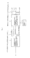
- Fig. 1 is a block diagram showing the structure of an embodiment of a measurement device that uses a wavelength-multiplexed optical signal measurement method according to the present invention.
- L represents a wavelength-multiplexed optical signal that is to be an optical signal to be measured.
- the wavelength-multiplexed optical signal L is formed by literally modulating light beams of wavelengths with different signals, and multiplexing those signals.
- the modulated signal corresponding to the frequency is represented by a i (t)
- the electrical field of a wavelength signal is expressed as:
- a i (t) is a complex number.
- the electrical field of a wavelength-multiplexed optical signal is b(t)
- the electrical field of the entire signal is the sum of the electrical fields of the respective wavelength signals, and can be expressed as:
- the minimum variation cycle is substantially equal to the inverse number of the bandwidth ⁇ f total of the entire wavelength-multiplexed optical signal. For example, in the case of a wavelength-multiplexed optical signal multiplexed at frequency intervals of 100 GHz, ⁇ f total is equal to 1 THz, and therefore, b(t) varies within the time of approximately 1 ps.
- This sequentially sampled electrical field sampling unit 11 measures the electrical field amplitude of measured optical signal L at M times at intervals of time T.
- the sequentially sampled electrical field sampling unit 11 measures b(t), b(t+T), b(t+2T), ..., and b(t+(M-1)T).
- T it is necessary to set T smaller than 1/ ⁇ f total .
- b(t) can be completely determined from the measured data string: b(t), b(t+T), b(t+2T), ..., and b(t+(M-1)T).
- b(t) is a complex number, and has a real part and a imaginary part. Therefore, the number of pieces of data obtained through this measurement process is 2M.
- 1/(MT) The inverse number 1/(MT) of the total observation time also needs to be set smaller than the frequency interval ⁇ f in the wavelength channels.
- 1/(MT) defines the smallest splittable frequency intervals when a wavelength-multiplexed optical signal is split according to the present invention. Measuring the amplitude of a wavelength-multiplexed optical signal is not possible in terms of speed by a conventional method involving a light receiving element, but can be realized by the following method.
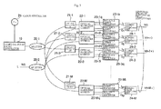
- Fig. 3 is a block diagram showing a specific structure of the above described sequentially sampled electrical field sampling unit 11.
- reference numeral 19 indicates a sampling pulse generator.
- Sampling pulse light L SP generated here is split into M lines by a splitter 20-1, and is supplied to one end of the input terminals of each of optical 90-degree hybrids 22-1 through 22-M via delay devices 21-1 through 21-M.
- the optical signal to be measured L that is wavelength-multiplexed is split into M lines by a splitter 20-2, and is supplied to the other end of the input terminals of each of the optical 90-degree hybrids 22-1 through 22-M.
- the delay devices 21-1 through 21-M each provide a time delay of an integral multiple of T such as 0, T, 2T, ..., (M-1)T in the path of split sampling pulse light, and may be placed in the split output path of the optical signal to be measured L.
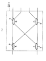
- the optical 90-degree hybrids 22-1 through 22-M are each formed with optical couplers a, b, c, and d, as shown in Fig. 4 .
- the difference between optical paths AB and AD in the drawing is set larger or smaller than the difference between optical paths CB and CD by ⁇ /4 ( ⁇ is a light wavelength).
- the pairs of optical signals obtained at the optical 90-degree hybrids 22-1 through 22-M are received by balanced light receiving elements 23-1 i through 23-M i and 23-1 q through 23-Mq, and are converted into electrical signals I 1 through I M and Q 1 through Q M .
- the converted signals are transmitted to numeric value computing units 24-1 through 24-M by the line.
- a clock generator 25 sets the clock slightly detuned from a part of a signal bit rate divided by an integer (approximately 1/10 through 1/1000, for example). More specifically, where F c represents the clock frequency,
- Patent Document 2 discloses a technique related to a light sampling method for observing locally-fast signal light that is repetitively input.
- the intensity modulation and frequency modulator in an optical signal are observed where one of the following conditions is satisfied: a first condition is that a light pulse generating unit generates sampling pulse light having a light pulse width shorter than the inverse number of the frequency variation of the signal light, and the intensity of the signal light hardly varies within the time of the pulse width of the sampling pulse light; a second condition is that the frequency of the optical signal to be measured L hardly varies within the time of the pulse width of the sampling pulse light L SP ; and a third condition is that the center frequency of the sampling pulse light L SP is substantially equal to the center frequency of the signal light. Accordingly, the electrical field amplitude of the optical signal can be determined from this intensity modulation and frequency modulator.
- the first and second conditions mean that the pulse width of the sampling pulse light L SP needs to be shorter than the variation time of the wavelength-multiplexed optical signal b(t) (the inverse number of ⁇ f total . This is equivalent to the spectral width of the sampling pulse light L SP being larger than ⁇ f total .
- the third condition means that the center frequency of the sampling pulse light L SP substantially matches the center wavelength of the entire wavelength-multiplexed optical signal.
- the spectral width of the sampling pulse light L SP to be used for sampling needs to cover the entire spectrum of the entire wavelength-multiplexed optical signal to be observed.
- the electrical field waveform Sam(t) of the sampling pulse light is set as:
- f s represents the center frequency of the sampling pulse light
- ⁇ s represents the initial phase of the sampling pulse light, the reference of which is the signal light.
- the amplitude of the sampling pulse light is standardized, and will be hereinafter expressed as follows including the phase:
- bm b(t+mT).
- the output light beams from the optical 90-degree hybrids 22-1 through 22-M are connected to the light receiving elements 23-1 i through 23-M i of the in-phase channel, and the light receiving elements 23-1 q through 23-Mq of the quadrature channel, and photocurrents I 1 through I M of the in-phase channel and photocurrents Q 1 through Q M of the quadrature channel are induced.
- the sizes of those photocurrents are expressed as:
- R and T represent a real part and an imaginary part, respectively.
- * represents the phase conjugate.
- the spectral width of each channel is smaller than the frequency interval ⁇ f between the channels, and this is true with respect to regular wavelength-multiplexed optical signals.
- the equation (7) is transformed into
- the total electrical field amplitude J m is in a Fourier transformation relationship with the amplitude a i (0) of each wavelength-multiplexed optical signal.
- the amplitude a i (0) of each wavelength channel can be determined by performing a Fourier inverse transforming operation on the total electrical field amplitude J m .
- the following calculation should be performed:
- the numeric value computing units 24-1 through 24-M shown in Fig. 3 calculate the total electrical field amplitude J m according to J m ⁇ I m +jQ m, which is based on the currents I m and Q m from the light receiving elements 23-m i and 23-mq.
- a sequentially sampled electrical field analyzing unit 12 calculates the signal amplitude a i (0) of each wavelength channel from the total electrical field amplitude J m , based on the equation (10).
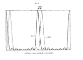
- the filter to be realized by performing a Fourier transformation can be substantially approximated by a sinc function (sin (x)/x) as shown in Fig. 5 , and has a transmission width of approximately 1/ (MT) and has a zero point every 1/ (2MT). Accordingly, where the adjacent channel interval ⁇ f is larger than 1/ (MT), signals of the respective channels can be separated. When the adjacent channel interval ⁇ f is equal to 1/(MT), the crosstalk can be minimized, as the center frequency of the adjacent channel is located at a zero point of the filter. The center frequency of the filter of each channel can be adjusted by varying f i in the equation (9).
- each delay time to be given by the delay devices 21-1 through 21-M is assumed to be exactly an integral multiple of T.
- a case where the time delays To through T M-1 to be realized by the delay devices 21-1 through 21-M in Fig. 3 are set as follows:
- ⁇ T m is a deviation from an ideal value of each delay.
- the sequentially sampled electrical field analyzing unit 12 stores J m (0) of the equation 15 obtained at a certain point of time into a memory unit 13.
- the sequentially sampled electrical field analyzing unit 12 extracts J m (0) from the memory unit 13 at the time of the calculation described below.
- Equation 16 K m ⁇ J m ⁇ J m 0 * Where the above is defined, the following is obtained from the equations (12) and (13):
- sampling pulse light is repetitively generated by the clock generator 25, and its generation frequency is slightly detuned from a part of the bit frequency divided by an integer. In this manner, the signal waveform (amplitude) at any time can be observed according to the principles of sampling oscilloscope.
- a wavelength-multiplexed optical signal can be observed by an entirely novel technique.
- the present invention enables an observation of a wavelength-multiplexed optical signal by an unconventional method by which Fourier analysis is numerically applied to a signal obtained by observing the total electrical field amplitude of the wavelength-multiplexed optical signal with an ultrafast observing unit. Accordingly, a wavelength-multiplexed optical signal can be observed without the use of an optical wavelength filter that is normally troublesome to be controlled.
Landscapes
- Physics & Mathematics (AREA)
- Spectroscopy & Molecular Physics (AREA)
- General Physics & Mathematics (AREA)
- Photometry And Measurement Of Optical Pulse Characteristics (AREA)
- Optical Communication System (AREA)
- Spectrometry And Color Measurement (AREA)
Abstract
Description
- The present invention relates to a measurement device and method for measuring the signal waveform at each wavelength of a wavelength-multiplexed optical signal.
- Conventionally, to measure the amplitude of a wavelength-multiplexed optical signal, the optical signal to be measured is normally split into optical signals of the respective wavelengths by a wavelength separation device, and the amplitude is then measured based on the signal waveforms of the respective wavelengths by a measurement device. The wavelength separation device may be a multilayer film optical filter or a diffraction grating disclosed in
Patent Document 1. However, in a case where wavelength intervals are set in a dense manner as in dense wavelength-multiplexed optical communications, to accurately perform a wavelength separation, the physical locations and temperatures of those elements need to be controlled with extremely high precision. -
- Patent Document 1: Japanese Patent Publication No.
3053294 - Patent Document 2: Japanese Patent Publication No.
3808820 - Although the following non-Patent Documents were issued after the application (Japanese Patent Application No.
2008-143480
Non-Patent Document 1: Keiji Okamoto and Fumihiko Ito, "Simultaneous WDM signal detection realized by ultrafast field sampling", Optics Express, Vol. 17, Issue 8, p.p. 6696-6702, published April 13, 2009.
Non-Patent Document 2: A material for presentation at ECOC 2008, which was held by the Convention of National Societies of Electrical Engineers of Europe (EUREL) in Brussels, Belgium, September 21-25, 2008: Keiji Okamoto and Fumihiko Ito, "Simultaneous WDM Signal Detection Realized by Ultrafast Field Sampling"
Non-Patent Document 3: A research paper at the 2008 IEICE Communications Society Conference held on September 16-19, 2008: Keiji Okamoto and Fumihiko Ito, "Simultaneous WDM Signal Detection Realized by Ultrafast Field Sampling" - As described above, to measure the signal amplitude at each wavelength of a conventional wavelength-multiplexed optical signal, the optical signal to be measured is split into optical signals of the respective wavelengths, and the optical signals of the respective wavelengths are extracted. The signal waveform of each of the optical signals is then measured. Therefore, in the case of optical signals having dense wavelength intervals, a high-precision wavelength separation device is required. Furthermore, the elements in the wavelength separation device need to be controlled with high precision, resulting in problems in costs and management.
- The present invention has been made in view of the above circumstances, and an object thereof is to provide a wavelength-multiplexed optical signal measurement device and the method thereof by which the signal amplitude at each wavelength of a wavelength-multiplexed optical signal can be measured without performing a wavelength separation, and optical signals having dense wavelength intervals can be processed.
- To achieve the above object, a wavelength-multiplexed optical signal measurement device according to the present invention has the following structure.
- (1) The wavelength-multiplexed optical signal measurement device includes: a sequentially sampled electrical field sampling unit that measures the total electrical field amplitude of a wavelength-multiplexed optical signal; and a sequentially sampled electrical field analyzing unit that applies Fourier analysis to the result of the measurement carried out by the sequentially sampled electrical field sampling unit, and calculates the electrical field amplitude of the signal component of each wavelength, the sequentially sampled electrical field sampling unit measuring the total electrical field amplitude Jm of the wavelength-multiplexed optical signal M times at intervals of time T (provided that, where the total bandwidth of the wavelength-multiplexed optical signal is Δftotal, the time T is set shorter than 1/Δftotal, and the
inverse number 1/(MT) of the total observation time is set smaller than the frequency interval Δf of adjacent wavelength channels), the sequentially sampled electrical field analyzing unit calculating the amplitude of the signal of each wavelength by determining a series of Fourier transformations of the total electrical field amplitude Jm (0 ≤ m ≤ M-1) determined by the sequentially sampled electrical field sampling unit. -
- (2) In the structure of (1), the sequentially sampled electrical field sampling unit includes: a light generating unit that generates sampling pulse light that has a spectral width larger than the total bandwidth Δftotal of the wavelength-multiplexed optical signal, and has a spectral center substantially matching the center wavelength of the entire wavelength-multiplexed optical signal light; a splitting unit that M-splits the sampling pulse light and the wavelength-multiplexed optical signal light; a delay unit that gives a time delay of an integral multiple of the time T in one of a path of the M-split sampling pulse light and a path of the wavelength-multiplexed optical signal light; M optical 90-degree hybrids that multiplex the sampling pulse light and the wavelength-multiplexed optical signal light at each split output after the splitting and delaying, and form signal light beams with phases separated 90 degrees from one another; M balance light receivers that receive light beams emitted from the M optical 90-degree hybrids, and obtain orthogonal currents Im and Qm (0 ≤ m ≤ M-1); and a computing unit that measures the values of the respective output currents Im and Qm of the M balance light receivers at arbitrary time, and determines the total electrical field amplitude Jm of the wavelength-multiplexed optical signal light according to Jm = Im+jQm.
-
- (3) In the structure of (2), when an error exists in the delay amount generated by the delay unit, the sequentially sampled electrical field sampling unit sets an electrical field amplitude obtained by observing a single wavelength of a constant amplitude beforehand as:
- Jm (0) (0 ≤ m ≤ M-1),
and sets the total electrical field amplitude of the wavelength-multiplexed optical signal as:- Jm (0 ≤ m ≤ M-1),
- with the total electrical field amplitude of the wavelength-multiplexed optical signal being regarded as:
- Km ≡ Jm Jm (0) * (* representing a phase conjugate).
- Jm (0) (0 ≤ m ≤ M-1),
-
- (4) In the structure of (2) or (3), the light generating unit repetitively generates the sampling pulse light, and detunes its generation frequency slightly from a part of the bit frequency divided by an integer.
A wavelength-multiplexed optical signal measurement method according to the present invention is implemented to carry out by the following procedures. -
- (5) The wavelength-multiplexed optical signal measurement method is designed for calculating the electrical field amplitude of the signal component of each wavelength by measuring the total electrical field amplitude of a wavelength-multiplexed optical signal and applying Fourier analysis to the result of the measurement, and includes the following procedures: measuring the total electrical field amplitude Jm of the wavelength-multiplexed optical signal M times at intervals of time T (provided that, where the total bandwidth of the wavelength-multiplexed optical signal is Δftotal, the time T is set shorter than 1/Δftotal, and the
inverse number 1/ (MT) of the total observation time is set smaller than the frequency interval Δf of adjacent wavelength channels), and applying Fourier analysis to the total electrical field amplitude Jm (0 ≤ m ≤ M-1), to calculate the amplitude of the signal of each wavelength. -
- (6) In the procedure of (5), the measurement of the total electrical field amplitude of the wavelength-multiplexed optical signal includes: generating sampling pulse light for the wavelength-multiplexed optical signal, the sampling pulse light having a spectral width larger than the total bandwidth Δftotal of the wavelength-multiplexed optical signal, the sampling pulse light having a spectral center substantially matching the center wavelength of the entire wavelength-multiplexed optical signal light; M-splitting the sampling pulse light and the wavelength-multiplexed optical signal; giving a time delay of an integral multiple of the time T in one of the path of the M-split sampling pulse light and the path of the wavelength-multiplexed optical signal; multiplexing the sampling pulse light and the wavelength-multiplexed optical signal at each split output after the splitting and delaying, and forming a pair of signal light beams with phases separated 90 degrees from each another; obtaining orthogonal currents Im and Qm (0 ≤ m ≤ M-1) of the pair of signal light beams; and measuring the values of the orthogonal currents Im and Qm at arbitrary time, and determining the total electrical field amplitude Jm of the wavelength-multiplexed optical signal according to Jm = Im+jQm.
-
- (7) In the procedure of (6), the measurement of the total electrical field amplitude of the wavelength-multiplexed optical signal includes: when an error exists in a delay amount generated by the delay unit, setting an electrical field amplitude obtained by observing a single wavelength of a constant amplitude beforehand as:
- Jm (0) (0 ≤ m ≤ M-1);
and setting the total electrical field amplitude of the wavelength-multiplexed optical signal as: - Jm (0 ≤ m ≤ M-1),
with the total electrical field amplitude of the wavelength-multiplexed optical signal being regarded as: - Km ≡ Jm Jm (0) * (* representing a phase conjugate).
- Jm (0) (0 ≤ m ≤ M-1);
-
- (8) In the procedures of (6) or (7), the sampling pulse light is repetitively generated, and its generation frequency is detuned slightly from a part of the bit frequency divided by an integer.
As described above, the wavelength-multiplexed optical signal measurement device and the method thereof having the above structure are characterized by measuring the total electrical field waveform of a wavelength-multiplexed optical signal with an ultrafast sequentially sampled electrical field sampling unit, and applying Fourier analysis to the measurement result, to calculate the electrical field waveforms of optical signals of the respective wavelengths. - As described above, the present invention can provide a wavelength-multiplexed optical signal measurement device and the method thereof by which the signal amplitude at each wavelength of a wavelength-multiplexed optical signal can be measured without performing a wavelength separation, and optical signals having dense wavelength intervals can be processed.
-
-
Fig. 1 is a block diagram showing the structure of an embodiment of a measurement device that uses a wavelength-multiplexed optical signal waveform measurement method according to the present invention. -
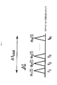
Fig. 2 is a drawing for explaining a wavelength-multiplexed signal that is the optical signal to be measured in the embodiment illustrated inFig. 1 . -
Fig. 3 is a block diagram showing the structure of a sequentially sampled electrical field sampling unit in the embodiment illustrated inFig. 1 . -
Fig. 4 is a block diagram showing a specific structure of an optical 90-degree hybrid illustrated inFig. 3 . -
Fig. 5 is a waveform chart for explaining the sinc function used in the above embodiment. - The following is a description of embodiments of the present invention, with reference to the accompanying drawings.
Fig. 1 is a block diagram showing the structure of an embodiment of a measurement device that uses a wavelength-multiplexed optical signal measurement method according to the present invention. InFig. 1 , L represents a wavelength-multiplexed optical signal that is to be an optical signal to be measured. The wavelength-multiplexed optical signal L is formed by literally modulating light beams of wavelengths with different signals, and multiplexing those signals. The frequency of the light beam of each wavelength is denoted by fi (i = 1, 2, ..., N). Where the modulated signal corresponding to the frequency is represented by ai(t), the electrical field of a wavelength signal is expressed as: -

In the equation, ai(t) is a complex number. Where the electrical field of a wavelength-multiplexed optical signal is b(t), the electrical field of the entire signal is the sum of the electrical fields of the respective wavelength signals, and can be expressed as: -

- The optical signal to be measured L (= b(t)) is guided to a sequentially sampled electrical
field sampling unit 11. This sequentially sampled electricalfield sampling unit 11 measures the electrical field amplitude of measured optical signal L at M times at intervals of time T. In other words, the sequentially sampled electricalfield sampling unit 11 measures b(t), b(t+T), b(t+2T), ..., and b(t+(M-1)T). - Here, it is necessary to set T smaller than 1/Δftotal. This is based on a sampling theorem, and only where the condition is satisfied, b(t) can be completely determined from the measured data string: b(t), b(t+T), b(t+2T), ..., and b(t+(M-1)T). Here, b(t) is a complex number, and has a real part and a imaginary part. Therefore, the number of pieces of data obtained through this measurement process is 2M.
- The
inverse number 1/(MT) of the total observation time also needs to be set smaller than the frequency interval Δf in the wavelength channels. As will be described later, 1/(MT) defines the smallest splittable frequency intervals when a wavelength-multiplexed optical signal is split according to the present invention.
Measuring the amplitude of a wavelength-multiplexed optical signal is not possible in terms of speed by a conventional method involving a light receiving element, but can be realized by the following method. -
Fig. 3 is a block diagram showing a specific structure of the above described sequentially sampled electricalfield sampling unit 11. InFig. 3 ,reference numeral 19 indicates a sampling pulse generator. Sampling pulse light LSP generated here is split into M lines by a splitter 20-1, and is supplied to one end of the input terminals of each of optical 90-degree hybrids 22-1 through 22-M via delay devices 21-1 through 21-M. Meanwhile, the optical signal to be measured L that is wavelength-multiplexed is split into M lines by a splitter 20-2, and is supplied to the other end of the input terminals of each of the optical 90-degree hybrids 22-1 through 22-M. - The delay devices 21-1 through 21-M each provide a time delay of an integral multiple of T such as 0, T, 2T, ..., (M-1)T in the path of split sampling pulse light, and may be placed in the split output path of the optical signal to be measured L.
The optical 90-degree hybrids 22-1 through 22-M are each formed with optical couplers a, b, c, and d, as shown inFig. 4 . The difference between optical paths AB and AD in the drawing is set larger or smaller than the difference between optical paths CB and CD by λ/4 (λ is a light wavelength). - The pairs of optical signals obtained at the optical 90-degree hybrids 22-1 through 22-M are received by balanced light receiving elements 23-1i through 23-Mi and 23-1q through 23-Mq, and are converted into electrical signals I1 through IM and Q1 through QM. The converted signals are transmitted to numeric value computing units 24-1 through 24-M by the line.
- All the wavelength channels for wavelength-multiplexed optical signals operate at bit rates (Bbps) that are synchronous with the same clock. Therefore, in the
optical sampling unit 11 illustrated inFig. 3 , aclock generator 25 sets the clock slightly detuned from a part of a signal bit rate divided by an integer (approximately 1/10 through 1/1000, for example). More specifically, where Fc represents the clock frequency, -

Here, ΔF represents detuned frequency. According to this clock, the sampling pulselight generating unit 19 generates the sampling pulse light LSP.
The sequentially sampled electricalfield sampling unit 11 having the above described structure is realized by applying the light sampling method and device disclosed inPatent Document 2.Patent Document 2 discloses a technique related to a light sampling method for observing locally-fast signal light that is repetitively input. By the technique, the intensity modulation and frequency modulator in an optical signal are observed where one of the following conditions is satisfied: a first condition is that a light pulse generating unit generates sampling pulse light having a light pulse width shorter than the inverse number of the frequency variation of the signal light, and the intensity of the signal light hardly varies within the time of the pulse width of the sampling pulse light; a second condition is that the frequency of the optical signal to be measured L hardly varies within the time of the pulse width of the sampling pulse light LSP; and a third condition is that the center frequency of the sampling pulse light LSP is substantially equal to the center frequency of the signal light. Accordingly, the electrical field amplitude of the optical signal can be determined from this intensity modulation and frequency modulator. - When the above first through third conditions are applied to the wavelength-multiplexed optical signal L (= b(t)), the first and second conditions mean that the pulse width of the sampling pulse light LSP needs to be shorter than the variation time of the wavelength-multiplexed optical signal b(t) (the inverse number of Δftotal. This is equivalent to the spectral width of the sampling pulse light LSP being larger than Δftotal.
- The third condition means that the center frequency of the sampling pulse light LSP substantially matches the center wavelength of the entire wavelength-multiplexed optical signal. To sum up those three conditions, the spectral width of the sampling pulse light LSP to be used for sampling needs to cover the entire spectrum of the entire wavelength-multiplexed optical signal to be observed.
- For ease of explanation hereafter, the electrical field waveform Sam(t) of the sampling pulse light is set as:
-

Here, δ(t) is a delta function that has an intensity only in the vicinity of t=0, and is zero in the other regions, and the sampling pulse light has an extremely short pulse width. Accordingly, this approximation can be performed. Further, fs represents the center frequency of the sampling pulse light, and φs represents the initial phase of the sampling pulse light, the reference of which is the signal light. For simplification, the amplitude of the sampling pulse light is standardized, and will be hereinafter expressed as follows including the phase: -

When the sampling pulse light is incident on the optical 90-degree hybrids 22-1 through 22-M, the delay devices 21-1 through 21-M give the delays of 0, T, 2T, ..., and (M-1)T, respectively. Accordingly, where t=t0 is set as the time at which the sampling pulse light reaches the first optical 90-degree hybrid 22-1, the amplitude Samm of the sampling pulse light incident on the mth optical 90-degree hybrid 22-m can be expressed as: -

Also, the amplitude bm (0 ≤ m ≤ M-1) of the wavelength-multiplexed optical signal at the time 0, T, 2T, ..., and (M-1)T at which the split sampling pulse light is incident on the respective optical 90-degree hybrids 22-1 through 22-M is expressed as: -

Here, bm = b(t+mT).
The output light beams from the optical 90-degree hybrids 22-1 through 22-M are connected to the light receiving elements 23-1i through 23-Mi of the in-phase channel, and the light receiving elements 23-1q through 23-Mq of the quadrature channel, and photocurrents I1 through IM of the in-phase channel and photocurrents Q1 through QM of the quadrature channel are induced. The sizes of those photocurrents are expressed as: -

Here, R and T represent a real part and an imaginary part, respectively. Also, * represents the phase conjugate. Where the equations (4) and (5) are substituted into the equation (6), and Jm ≡ Im+jQm, the following equation is established: -

For simplification, a case where the amplitude ai(mT) of each wavelength channel hardly varies during time MT is now described. Here, the spectral width of each channel is smaller than the frequency interval Δf between the channels, and this is true with respect to regular wavelength-multiplexed optical signals. In that case, the equation (7) is transformed into -

where Jm ≡ Im+jQm is proportional to the electrical field amplitude b(t) at time t=0.
In view of the above, the total electrical field amplitude Jm is in a Fourier transformation relationship with the amplitude ai(0) of each wavelength-multiplexed optical signal. Accordingly, the amplitude ai(0) of each wavelength channel can be determined by performing a Fourier inverse transforming operation on the total electrical field amplitude Jm. In other words, to determine the amplitude ai(0), the following calculation should be performed: -

Because of the fundamental properties of a Fourier transformation, the following relationship should be established to sufficiently separate the channels: -

Therefore, Δf should be equal to or larger than 1/(MT), and the adj acent frequency interval Δf=fi-fi-1should be larger by as much as 1/(MT).
The numeric value computing units 24-1 through 24-M shown inFig. 3 calculate the total electrical field amplitude Jm according to Jm ≡ Im+jQm, which is based on the currents Im and Qm from the light receiving elements 23-mi and 23-mq. A sequentially sampled electricalfield analyzing unit 12 calculates the signal amplitude ai(0) of each wavelength channel from the total electrical field amplitude Jm, based on the equation (10). - Here, the filter to be realized by performing a Fourier transformation can be substantially approximated by a sinc function (sin (x)/x) as shown in
Fig. 5 , and has a transmission width of approximately 1/ (MT) and has a zero point every 1/ (2MT). Accordingly, where the adjacent channel interval Δf is larger than 1/ (MT), signals of the respective channels can be separated. When the adjacent channel interval Δf is equal to 1/(MT), the crosstalk can be minimized, as the center frequency of the adjacent channel is located at a zero point of the filter. The center frequency of the filter of each channel can be adjusted by varying fi in the equation (9). - In the explanation made so far, each delay time to be given by the delay devices 21-1 through 21-M is assumed to be exactly an integral multiple of T. However, in embodying the present invention, it is necessary to take into consideration the fact that there might be a variation in the delay time.
Here, a case where the time delays To through TM-1 to be realized by the delay devices 21-1 through 21-M inFig. 3 are set as follows: -

Here, ΔTm is a deviation from an ideal value of each delay. At this point, the equation (8) can be transformed into -

Since a coefficient exp(-j2πmfsΔTm) is generated by the deviation from the ideal delay value, the correct ai(0) cannot be obtained by applying Fourier analysis to that.
In such a case, the coefficient exp(-j2πmfsΔTm) is measured beforehand by the unit described below, and is corrected through a numeric value computing operation. Specifically, in the structure illustrated inFig. 1 , only a single wavelength light beam of constant amplitude is observed. If a1(0) is measured, Jm (0) to be output is expressed as follows: -

The sequentially sampled electricalfield analyzing unit 12 stores Jm (0) of the equation 15 obtained at a certain point of time into amemory unit 13. The sequentially sampled electricalfield analyzing unit 12 extracts Jm (0) from thememory unit 13 at the time of the calculation described below. -

Where the above is defined, the following is obtained from the equations (12) and (13): -

Accordingly, -

ai(0) can be determined by the above Fourier analysis.
As is apparent from the above explanation, according to this embodiment, the amplitude of each wavelength channel can be detected at the single time t=0. Specifically, as shown inFig. 3 , sampling pulse light is repetitively generated by theclock generator 25, and its generation frequency is slightly detuned from a part of the bit frequency divided by an integer. In this manner, the signal waveform (amplitude) at any time can be observed according to the principles of sampling oscilloscope. - As described above, according to the present invention, a wavelength-multiplexed optical signal can be observed by an entirely novel technique. The present invention enables an observation of a wavelength-multiplexed optical signal by an unconventional method by which Fourier analysis is numerically applied to a signal obtained by observing the total electrical field amplitude of the wavelength-multiplexed optical signal with an ultrafast observing unit. Accordingly, a wavelength-multiplexed optical signal can be observed without the use of an optical wavelength filter that is normally troublesome to be controlled.
- The present invention is not limited to the above described embodiment, but modifications may be made to the components in the embodying stage without departing from the scope of the invention. Also, various inventions can be made by arbitrarily combining two or more of the components disclosed in the above described embodiment. For example, some of the components described in the embodiment may be deleted. Further, components disclosed in different embodiments may be arbitrarily combined.
-
- 11
- sequentially sampled electrical field sampling unit
- 12
- sequentially sampled electrical field analyzing unit
- 19
- sampling pulse generator
- 20-1, 20-2
- splitters
- 21-1
- through
- 21-M
- delay devices
- 22-1 through 22-M
- optical 90-degree hybrids
- a, b, c, d
- optical couplers
- 23-1i through 23-Mi, 23-1q through 23-Mq
- balance light receiving elements
- 24-1 through 24-M
- numeric value computing units
- 25
- clock generator
Claims (8)
- A wavelength-multiplexed optical signal measurement device comprising:a sequentially sampled electrical field sampling unit that measures a total electrical field amplitude of a wavelength-multiplexed optical signal; anda sequentially sampled electrical field analyzing unit that applies Fourier analysis to a result of the measurement carried out by the sequentially sampled electrical field sampling unit, and calculates an electrical field amplitude of a signal component of each wavelength,the sequentially sampled electrical field sampling unit measuring the total electrical field amplitude Jm of the wavelength-multiplexed optical signal M times at intervals of time T (provided that, where a total bandwidth of the wavelength-multiplexed optical signal is Δftotal, the time T is set shorter than 1/Δftotal, and the inverse number 1/(MT) of a total observation time is set smaller than a frequency interval Δf of an adjacent wavelength channel),the sequentially sampled electrical field analyzing unit calculating an amplitude of a signal of each wavelength by determining a series of Fourier transformations of the total electrical field amplitude Jm (0 ≤ m ≤ M-1) determined by the sequentially sampled electrical field sampling unit.
- The wavelength-multiplexed optical signal measurement device according to claim 1, wherein
the sequentially sampled electrical field sampling unit includes:a light generating unit that generates sampling pulse light that has a spectral width larger than the total bandwidth Δftotal of the wavelength-multiplexed optical signal, and has a spectral center substantially matching a center wavelength of the entire wavelength-multiplexed optical signal light;a splitting unit that M-splits the sampling pulse light and the wavelength-multiplexed optical signal light;a delay unit that gives a time delay of an integral multiple of the time T in one of a path of the M-split sampling pulse light and a path of the wavelength-multiplexed optical signal light;M optical 90-degree hybrids that multiplex the sampling pulse light and the wavelength-multiplexed optical signal light at each split output after the splitting and delaying, and form signal light beams with phases separated 90 degrees from one another;M balance light receivers that receive light beams emitted from the M optical 90-degree hybrids, and obtain orthogonal currents Im and Qm (0 ≤ m ≤ M-1); anda computing unit that measures values of the output currents Im and Qm of the M balance receivers at an arbitrary time, and determines the total electrical field amplitude Jm of the wavelength-multiplexed optical signal light according to Jm = Im+JQm. - The wavelength-multiplexed optical signal measurement device according to claim 2, wherein
when an error exists in a delay amount generated by the delay unit, the sequentially sampled electrical field sampling unit sets an electrical field amplitude obtained by observing a single wavelength of a constant amplitude beforehand as:Jm (0) (0 ≤ m ≤ M-1),and sets the total electrical field amplitude of the wavelength-multiplexed optical signal as:Jm (0 ≤ m ≤ M-1),with the total electrical field amplitude of the wavelength-multiplexed optical signal being regarded as:Km ≡ Jm Jm (0) * (* representing a phase conjugate). - The wavelength-multiplexed optical signal measurement device according to claim 2 or 3, wherein the light generating unit repetitively generates the sampling pulse light, and detunes a generation frequency thereof slightly from a part of a bit frequency divided by an integer.
- A wavelength-multiplexed optical signal measurement method for calculating an electrical field amplitude of a signal component of each wavelength by measuring a total electrical field amplitude of a wavelength-multiplexed optical signal and applying Fourier analysis to a result of the measurement,
the method comprising
measuring the total electrical field amplitude Jm of the wavelength-multiplexed optical signal M times at intervals of time T (provided that, where a total bandwidth of the wavelength-multiplexed optical signal is Δftotal, the time T is set shorter than 1/Δftotal, and the inverse number 1/(MT) of a total observation time is set smaller than a frequency interval Δf of an adjacent wavelength channel), and applying Fourier analysis to the total electrical field amplitude Jm (0 ≤ m ≤ M-1), to calculate the amplitude of the signal of each wavelength. - The wavelength-multiplexed optical signal measurement method according to claim 5, wherein
the measurement of the total electrical field amplitude of the wavelength-multiplexed optical signal includes:generating sampling pulse light for the wavelength-multiplexed optical signal, the sampling pulse light having a spectral width larger than the total bandwidth Δftotal of the wavelength-multiplexed optical signal, the sampling pulse light having a spectral center substantially matching a center wavelength of the entire wavelength-multiplexed optical signal light;M-splitting the sampling pulse light and the wavelength-multiplexed optical signal;giving a time delay of an integral multiple of the time T in one of a path of the M-split sampling pulse light and a path of the wavelength-multiplexed optical signal;multiplexing the sampling pulse light and the wavelength-multiplexed optical signal at each split output after the splitting and delaying, and forming a pair of signal light beams with phases separated 90 degrees from each another;obtaining orthogonal currents Im and Qm (0 ≤ m ≤ M-1) of the pair of signal light beams; andmeasuring values of the orthogonal currents Im and Qm at arbitrary time, and determining the total electrical field amplitude Jm of the wavelength-multiplexed optical signal according to Jm = Im+jQm. - The wavelength-multiplexed optical signal measurement method according to claim 6, wherein
the measurement of the total electrical field amplitude of the wavelength-multiplexed optical signal includes:when an error exists in a delay amount generated by the time delay, setting an electrical field amplitude obtained by observing a single wavelength of a constant amplitude beforehand as:Jm (0) (0 ≤ m ≤ M-1);and setting the total electrical field amplitude of the wavelength-multiplexed optical signal as:Jm (0 ≤ m ≤ M-1),with the total electrical field amplitude of the wavelength-multiplexed optical signal being regarded as:Km ≡ Jm Jm (0) * (* representing a phase conjugate). - The wavelength-multiplexed optical signal measurement method according to claim 6 or 7, wherein the sampling pulse light is repetitively generated, and a generation frequency thereof is detuned slightly from a part of a bit frequency divided by an integer.
Applications Claiming Priority (2)
| Application Number | Priority Date | Filing Date | Title |
|---|---|---|---|
| JP2008143480 | 2008-05-30 | ||
| PCT/JP2009/059010 WO2009145070A1 (en) | 2008-05-30 | 2009-05-14 | Wavelength‑multiplexed signal measurement device and method |
Publications (3)
| Publication Number | Publication Date |
|---|---|
| EP2284513A1 true EP2284513A1 (en) | 2011-02-16 |
| EP2284513A4 EP2284513A4 (en) | 2011-05-11 |
| EP2284513B1 EP2284513B1 (en) | 2012-01-04 |
Family
ID=41376951
Family Applications (1)
| Application Number | Title | Priority Date | Filing Date |
|---|---|---|---|
| EP09754578A Not-in-force EP2284513B1 (en) | 2008-05-30 | 2009-05-14 | Wavelength multiplexed signal measurement device and method |
Country Status (6)
| Country | Link |
|---|---|
| US (1) | US8401808B2 (en) |
| EP (1) | EP2284513B1 (en) |
| JP (1) | JP4949514B2 (en) |
| CN (1) | CN102027345B (en) |
| AT (1) | ATE540294T1 (en) |
| WO (1) | WO2009145070A1 (en) |
Families Citing this family (7)
| Publication number | Priority date | Publication date | Assignee | Title |
|---|---|---|---|---|
| JP2014045096A (en) * | 2012-08-27 | 2014-03-13 | Nippon Telegr & Teleph Corp <Ntt> | Laser phase noise measuring apparatus and measuring method |
| US20140193155A1 (en) * | 2013-01-10 | 2014-07-10 | The Regents Of The University Of Colorado, A Body Corporate | Microphotonic Coupled-Resonator Devices |
| JP6442884B2 (en) | 2014-06-25 | 2018-12-26 | 富士通株式会社 | Optical transmission system, optical transmission device, and wavelength interval measuring device |
| JP6230029B2 (en) * | 2015-02-09 | 2017-11-15 | 日本電信電話株式会社 | Apparatus and method for measuring impulse response of optical device |
| GB2581490A (en) * | 2019-02-18 | 2020-08-26 | Secr Defence | Method and device for measuring a pulse signal with high dynamic range |
| JP7454183B2 (en) * | 2020-08-27 | 2024-03-22 | 日本電信電話株式会社 | Spectrometer and spectrometer measurement method |
| CN115956192B (en) * | 2020-09-11 | 2025-07-29 | 日本电信电话株式会社 | Vibration detection device and vibration detection method |
Family Cites Families (11)
| Publication number | Priority date | Publication date | Assignee | Title |
|---|---|---|---|---|
| JPS6084388A (en) | 1983-10-14 | 1985-05-13 | Teikoku Chem Ind Corp Ltd | Liquid crystal compound |
| US5053760A (en) | 1989-07-17 | 1991-10-01 | The Grass Valley Group, Inc. | Graphics path prediction display |
| JP3053294B2 (en) | 1992-05-18 | 2000-06-19 | 日本電信電話株式会社 | Optical multiplexer / demultiplexer |
| DE60134422D1 (en) * | 2000-12-30 | 2008-07-24 | Lot 41 Acquisition Foundation | Carrier Interferometer Coding and Multiprocessing |
| JP3789784B2 (en) * | 2001-08-06 | 2006-06-28 | 日本電信電話株式会社 | Optical orthogonal frequency division multiplexing transmission system and transmission method |
| US7113702B2 (en) * | 2001-08-06 | 2006-09-26 | Nippon Telegraph And Telephone Corporation | Wavelength division multiplexing optical transmission system and transmission method |
| JP3808820B2 (en) | 2002-10-08 | 2006-08-16 | 日本電信電話株式会社 | Optical sampling method, apparatus and program |
| JP4439857B2 (en) | 2003-08-25 | 2010-03-24 | 独立行政法人科学技術振興機構 | Optical pulse phase measuring method and apparatus |
| JP4565198B2 (en) * | 2005-03-01 | 2010-10-20 | 国立大学法人大阪大学 | High resolution and high speed terahertz spectrometer |
| EP2067290B1 (en) * | 2006-09-30 | 2012-06-13 | Huawei Technologies Co., Ltd. | Optical identification demodulation system |
| JP4327839B2 (en) | 2006-12-13 | 2009-09-09 | 本田技研工業株式会社 | Assembly method for aluminum alloy wings |
-
2009
- 2009-05-14 US US12/990,741 patent/US8401808B2/en active Active
- 2009-05-14 JP JP2010514438A patent/JP4949514B2/en not_active Expired - Fee Related
- 2009-05-14 WO PCT/JP2009/059010 patent/WO2009145070A1/en not_active Ceased
- 2009-05-14 CN CN200980117708.2A patent/CN102027345B/en not_active Expired - Fee Related
- 2009-05-14 AT AT09754578T patent/ATE540294T1/en active
- 2009-05-14 EP EP09754578A patent/EP2284513B1/en not_active Not-in-force
Non-Patent Citations (3)
| Title |
|---|
| KEIJI OKAMOTO ET AL: "Relatively Delayed Dual-channel Interferometric Sampling for Observing Ultrafast Amplitude and Phase Modulation", PROCEEDINGS / ECOC 2006, 32ND EUROPEAN CONFERENCE ON OPTICAL COMMUNICATION : 24 - 28 SEPTEMBER 2006, CANNES, FRANCE, SEE, PARIS, FRANCE, 24 September 2006 (2006-09-24), pages 1-2, XP031437078, ISBN: 978-2-912328-39-7 * |
| KEIJI OKAMOTO ET AL: "Ultrafast sampling of complex polarization components for characterizing polarization mode dispersion", OPTICAL FIBER COMMUNICATION CONFERENCE AND EXPOSITION NATIONAL FIBER OPTIC ENGINEERS CONFERENCE. OFCNFOEC 2007, 25-29 MARCH 2007, ANAHEIM, CA, USA, IEEE, PISCATAWAY, NJ, USA, 1 March 2007 (2007-03-01), pages 1-3, XP031146794, ISBN: 978-1-55752-831-5 * |
| See also references of WO2009145070A1 * |
Also Published As
| Publication number | Publication date |
|---|---|
| US8401808B2 (en) | 2013-03-19 |
| US20110077887A1 (en) | 2011-03-31 |
| ATE540294T1 (en) | 2012-01-15 |
| EP2284513B1 (en) | 2012-01-04 |
| CN102027345A (en) | 2011-04-20 |
| EP2284513A4 (en) | 2011-05-11 |
| CN102027345B (en) | 2012-04-25 |
| JP4949514B2 (en) | 2012-06-13 |
| JPWO2009145070A1 (en) | 2011-10-06 |
| WO2009145070A1 (en) | 2009-12-03 |
Similar Documents
| Publication | Publication Date | Title |
|---|---|---|
| EP2284513B1 (en) | Wavelength multiplexed signal measurement device and method | |
| US11630368B2 (en) | Radio frequency passband signal generation using photonics | |
| US11567351B2 (en) | Methods for computation-free wideband spectral correlation and analysis | |
| CN104101484B (en) | Optical device measuring method based on double sideband modulation and measurement apparatus | |
| CN107528638B (en) | Broadband microwave signal arrival angle estimation method based on microwave photon filtering | |
| CN104990690B (en) | A kind of optical device frequency response measurement apparatus and method | |
| WO2020232790A1 (en) | Information real-time measurement system for ultrafast optical field | |
| US12003272B2 (en) | Timing measurement apparatus | |
| WO2020232787A1 (en) | Method and system for acquiring frequency domain information of ultra-fast optical field | |
| US10209135B2 (en) | Method for measuring multi-channel mismatch of ultra-high speed photonic sampler and measurement compensation device thereof | |
| US20030030865A1 (en) | Wavelength division multiplexing optical transmission system and transmission method | |
| EP1833181B1 (en) | Optical waveform measurement apparatus and optical waveform measurement method | |
| Rhodes et al. | Validating data analysis of broadband laser ranging | |
| CN113503904A (en) | System and method for measuring frequency response of photoelectric detector | |
| US12132514B2 (en) | Method and system for generating the spectrogram of a signal | |
| CN103107841B (en) | Optical device measuring method and device based on polarization deflection interfering method | |
| EP4689581A1 (en) | An optical detection system | |
| JP4916347B2 (en) | Optical heterodyne OFDR device | |
| JP5271791B2 (en) | Optical signal waveform measuring method, apparatus and program | |
| EP2495541A1 (en) | Relative phase detector, relative phase detecting method and information reading device | |
| JP2013038679A (en) | Wavelength multiplexed signal measurement device and measurement method thereof | |
| JP2013183214A (en) | Optical signal inspection device and optical signal inspection method | |
| US20220268931A1 (en) | Measurement apparatus and measurement method | |
| JP2005017129A (en) | Chromatic dispersion measurement device | |
| JP5927079B2 (en) | Laser light characteristic measuring method and measuring apparatus |
Legal Events
| Date | Code | Title | Description |
|---|---|---|---|
| PUAI | Public reference made under article 153(3) epc to a published international application that has entered the european phase |
Free format text: ORIGINAL CODE: 0009012 |
|
| 17P | Request for examination filed |
Effective date: 20101116 |
|
| AK | Designated contracting states |
Kind code of ref document: A1 Designated state(s): AT BE BG CH CY CZ DE DK EE ES FI FR GB GR HR HU IE IS IT LI LT LU LV MC MK MT NL NO PL PT RO SE SI SK TR |
|
| AX | Request for extension of the european patent |
Extension state: AL BA RS |
|
| A4 | Supplementary search report drawn up and despatched |
Effective date: 20110413 |
|
| RIC1 | Information provided on ipc code assigned before grant |
Ipc: G01J 11/00 20060101AFI20110512BHEP Ipc: G01J 3/28 20060101ALI20110512BHEP |
|
| GRAP | Despatch of communication of intention to grant a patent |
Free format text: ORIGINAL CODE: EPIDOSNIGR1 |
|
| DAX | Request for extension of the european patent (deleted) | ||
| GRAS | Grant fee paid |
Free format text: ORIGINAL CODE: EPIDOSNIGR3 |
|
| GRAA | (expected) grant |
Free format text: ORIGINAL CODE: 0009210 |
|
| AK | Designated contracting states |
Kind code of ref document: B1 Designated state(s): AT BE BG CH CY CZ DE DK EE ES FI FR GB GR HR HU IE IS IT LI LT LU LV MC MK MT NL NO PL PT RO SE SI SK TR |
|
| REG | Reference to a national code |
Ref country code: GB Ref legal event code: FG4D |
|
| REG | Reference to a national code |
Ref country code: CH Ref legal event code: EP |
|
| REG | Reference to a national code |
Ref country code: AT Ref legal event code: REF Ref document number: 540294 Country of ref document: AT Kind code of ref document: T Effective date: 20120115 |
|
| REG | Reference to a national code |
Ref country code: IE Ref legal event code: FG4D |
|
| REG | Reference to a national code |
Ref country code: DE Ref legal event code: R096 Ref document number: 602009004579 Country of ref document: DE Effective date: 20120308 |
|
| REG | Reference to a national code |
Ref country code: NL Ref legal event code: VDEP Effective date: 20120104 |
|
| PG25 | Lapsed in a contracting state [announced via postgrant information from national office to epo] |
Ref country code: SI Free format text: LAPSE BECAUSE OF FAILURE TO SUBMIT A TRANSLATION OF THE DESCRIPTION OR TO PAY THE FEE WITHIN THE PRESCRIBED TIME-LIMIT Effective date: 20120104 |
|
| LTIE | Lt: invalidation of european patent or patent extension |
Effective date: 20120104 |
|
| PG25 | Lapsed in a contracting state [announced via postgrant information from national office to epo] |
Ref country code: NO Free format text: LAPSE BECAUSE OF FAILURE TO SUBMIT A TRANSLATION OF THE DESCRIPTION OR TO PAY THE FEE WITHIN THE PRESCRIBED TIME-LIMIT Effective date: 20120404 Ref country code: LT Free format text: LAPSE BECAUSE OF FAILURE TO SUBMIT A TRANSLATION OF THE DESCRIPTION OR TO PAY THE FEE WITHIN THE PRESCRIBED TIME-LIMIT Effective date: 20120104 Ref country code: BE Free format text: LAPSE BECAUSE OF FAILURE TO SUBMIT A TRANSLATION OF THE DESCRIPTION OR TO PAY THE FEE WITHIN THE PRESCRIBED TIME-LIMIT Effective date: 20120104 Ref country code: IS Free format text: LAPSE BECAUSE OF FAILURE TO SUBMIT A TRANSLATION OF THE DESCRIPTION OR TO PAY THE FEE WITHIN THE PRESCRIBED TIME-LIMIT Effective date: 20120504 Ref country code: BG Free format text: LAPSE BECAUSE OF FAILURE TO SUBMIT A TRANSLATION OF THE DESCRIPTION OR TO PAY THE FEE WITHIN THE PRESCRIBED TIME-LIMIT Effective date: 20120404 Ref country code: HR Free format text: LAPSE BECAUSE OF FAILURE TO SUBMIT A TRANSLATION OF THE DESCRIPTION OR TO PAY THE FEE WITHIN THE PRESCRIBED TIME-LIMIT Effective date: 20120104 Ref country code: NL Free format text: LAPSE BECAUSE OF FAILURE TO SUBMIT A TRANSLATION OF THE DESCRIPTION OR TO PAY THE FEE WITHIN THE PRESCRIBED TIME-LIMIT Effective date: 20120104 |
|
| PG25 | Lapsed in a contracting state [announced via postgrant information from national office to epo] |
Ref country code: GR Free format text: LAPSE BECAUSE OF FAILURE TO SUBMIT A TRANSLATION OF THE DESCRIPTION OR TO PAY THE FEE WITHIN THE PRESCRIBED TIME-LIMIT Effective date: 20120405 Ref country code: LV Free format text: LAPSE BECAUSE OF FAILURE TO SUBMIT A TRANSLATION OF THE DESCRIPTION OR TO PAY THE FEE WITHIN THE PRESCRIBED TIME-LIMIT Effective date: 20120104 Ref country code: FI Free format text: LAPSE BECAUSE OF FAILURE TO SUBMIT A TRANSLATION OF THE DESCRIPTION OR TO PAY THE FEE WITHIN THE PRESCRIBED TIME-LIMIT Effective date: 20120104 Ref country code: PT Free format text: LAPSE BECAUSE OF FAILURE TO SUBMIT A TRANSLATION OF THE DESCRIPTION OR TO PAY THE FEE WITHIN THE PRESCRIBED TIME-LIMIT Effective date: 20120504 Ref country code: PL Free format text: LAPSE BECAUSE OF FAILURE TO SUBMIT A TRANSLATION OF THE DESCRIPTION OR TO PAY THE FEE WITHIN THE PRESCRIBED TIME-LIMIT Effective date: 20120104 |
|
| REG | Reference to a national code |
Ref country code: AT Ref legal event code: MK05 Ref document number: 540294 Country of ref document: AT Kind code of ref document: T Effective date: 20120104 |
|
| PG25 | Lapsed in a contracting state [announced via postgrant information from national office to epo] |
Ref country code: CY Free format text: LAPSE BECAUSE OF FAILURE TO SUBMIT A TRANSLATION OF THE DESCRIPTION OR TO PAY THE FEE WITHIN THE PRESCRIBED TIME-LIMIT Effective date: 20120104 |
|
| PG25 | Lapsed in a contracting state [announced via postgrant information from national office to epo] |
Ref country code: RO Free format text: LAPSE BECAUSE OF FAILURE TO SUBMIT A TRANSLATION OF THE DESCRIPTION OR TO PAY THE FEE WITHIN THE PRESCRIBED TIME-LIMIT Effective date: 20120104 Ref country code: SE Free format text: LAPSE BECAUSE OF FAILURE TO SUBMIT A TRANSLATION OF THE DESCRIPTION OR TO PAY THE FEE WITHIN THE PRESCRIBED TIME-LIMIT Effective date: 20120104 Ref country code: CZ Free format text: LAPSE BECAUSE OF FAILURE TO SUBMIT A TRANSLATION OF THE DESCRIPTION OR TO PAY THE FEE WITHIN THE PRESCRIBED TIME-LIMIT Effective date: 20120104 Ref country code: DK Free format text: LAPSE BECAUSE OF FAILURE TO SUBMIT A TRANSLATION OF THE DESCRIPTION OR TO PAY THE FEE WITHIN THE PRESCRIBED TIME-LIMIT Effective date: 20120104 Ref country code: EE Free format text: LAPSE BECAUSE OF FAILURE TO SUBMIT A TRANSLATION OF THE DESCRIPTION OR TO PAY THE FEE WITHIN THE PRESCRIBED TIME-LIMIT Effective date: 20120104 |
|
| PLBE | No opposition filed within time limit |
Free format text: ORIGINAL CODE: 0009261 |
|
| STAA | Information on the status of an ep patent application or granted ep patent |
Free format text: STATUS: NO OPPOSITION FILED WITHIN TIME LIMIT |
|
| PG25 | Lapsed in a contracting state [announced via postgrant information from national office to epo] |
Ref country code: IT Free format text: LAPSE BECAUSE OF FAILURE TO SUBMIT A TRANSLATION OF THE DESCRIPTION OR TO PAY THE FEE WITHIN THE PRESCRIBED TIME-LIMIT Effective date: 20120104 Ref country code: SK Free format text: LAPSE BECAUSE OF FAILURE TO SUBMIT A TRANSLATION OF THE DESCRIPTION OR TO PAY THE FEE WITHIN THE PRESCRIBED TIME-LIMIT Effective date: 20120104 |
|
| 26N | No opposition filed |
Effective date: 20121005 |
|
| PG25 | Lapsed in a contracting state [announced via postgrant information from national office to epo] |
Ref country code: MC Free format text: LAPSE BECAUSE OF NON-PAYMENT OF DUE FEES Effective date: 20120531 |
|
| PG25 | Lapsed in a contracting state [announced via postgrant information from national office to epo] |
Ref country code: AT Free format text: LAPSE BECAUSE OF FAILURE TO SUBMIT A TRANSLATION OF THE DESCRIPTION OR TO PAY THE FEE WITHIN THE PRESCRIBED TIME-LIMIT Effective date: 20120104 |
|
| REG | Reference to a national code |
Ref country code: DE Ref legal event code: R097 Ref document number: 602009004579 Country of ref document: DE Effective date: 20121005 |
|
| REG | Reference to a national code |
Ref country code: IE Ref legal event code: MM4A |
|
| PG25 | Lapsed in a contracting state [announced via postgrant information from national office to epo] |
Ref country code: MK Free format text: LAPSE BECAUSE OF FAILURE TO SUBMIT A TRANSLATION OF THE DESCRIPTION OR TO PAY THE FEE WITHIN THE PRESCRIBED TIME-LIMIT Effective date: 20120104 |
|
| PG25 | Lapsed in a contracting state [announced via postgrant information from national office to epo] |
Ref country code: IE Free format text: LAPSE BECAUSE OF NON-PAYMENT OF DUE FEES Effective date: 20120514 Ref country code: ES Free format text: LAPSE BECAUSE OF FAILURE TO SUBMIT A TRANSLATION OF THE DESCRIPTION OR TO PAY THE FEE WITHIN THE PRESCRIBED TIME-LIMIT Effective date: 20120415 |
|
| PG25 | Lapsed in a contracting state [announced via postgrant information from national office to epo] |
Ref country code: MT Free format text: LAPSE BECAUSE OF FAILURE TO SUBMIT A TRANSLATION OF THE DESCRIPTION OR TO PAY THE FEE WITHIN THE PRESCRIBED TIME-LIMIT Effective date: 20120104 |
|
| REG | Reference to a national code |
Ref country code: CH Ref legal event code: PL |
|
| PG25 | Lapsed in a contracting state [announced via postgrant information from national office to epo] |
Ref country code: LI Free format text: LAPSE BECAUSE OF NON-PAYMENT OF DUE FEES Effective date: 20130531 Ref country code: CH Free format text: LAPSE BECAUSE OF NON-PAYMENT OF DUE FEES Effective date: 20130531 |
|
| PG25 | Lapsed in a contracting state [announced via postgrant information from national office to epo] |
Ref country code: TR Free format text: LAPSE BECAUSE OF FAILURE TO SUBMIT A TRANSLATION OF THE DESCRIPTION OR TO PAY THE FEE WITHIN THE PRESCRIBED TIME-LIMIT Effective date: 20120104 |
|
| PG25 | Lapsed in a contracting state [announced via postgrant information from national office to epo] |
Ref country code: LU Free format text: LAPSE BECAUSE OF NON-PAYMENT OF DUE FEES Effective date: 20120514 |
|
| PG25 | Lapsed in a contracting state [announced via postgrant information from national office to epo] |
Ref country code: HU Free format text: LAPSE BECAUSE OF FAILURE TO SUBMIT A TRANSLATION OF THE DESCRIPTION OR TO PAY THE FEE WITHIN THE PRESCRIBED TIME-LIMIT Effective date: 20090514 |
|
| REG | Reference to a national code |
Ref country code: FR Ref legal event code: PLFP Year of fee payment: 8 |
|
| REG | Reference to a national code |
Ref country code: FR Ref legal event code: PLFP Year of fee payment: 9 |
|
| REG | Reference to a national code |
Ref country code: FR Ref legal event code: PLFP Year of fee payment: 10 |
|
| PGFP | Annual fee paid to national office [announced via postgrant information from national office to epo] |
Ref country code: DE Payment date: 20180522 Year of fee payment: 10 |
|
| PGFP | Annual fee paid to national office [announced via postgrant information from national office to epo] |
Ref country code: FR Payment date: 20180522 Year of fee payment: 10 |
|
| PGFP | Annual fee paid to national office [announced via postgrant information from national office to epo] |
Ref country code: GB Payment date: 20180518 Year of fee payment: 10 |
|
| REG | Reference to a national code |
Ref country code: DE Ref legal event code: R119 Ref document number: 602009004579 Country of ref document: DE |
|
| GBPC | Gb: european patent ceased through non-payment of renewal fee |
Effective date: 20190514 |
|
| PG25 | Lapsed in a contracting state [announced via postgrant information from national office to epo] |
Ref country code: GB Free format text: LAPSE BECAUSE OF NON-PAYMENT OF DUE FEES Effective date: 20190514 Ref country code: DE Free format text: LAPSE BECAUSE OF NON-PAYMENT OF DUE FEES Effective date: 20191203 |
|
| PG25 | Lapsed in a contracting state [announced via postgrant information from national office to epo] |
Ref country code: FR Free format text: LAPSE BECAUSE OF NON-PAYMENT OF DUE FEES Effective date: 20190531 |