EP2283576B1 - Integrated ramp, sweep fractional frequency synthesizer on an integrated circuit chip - Google Patents
Integrated ramp, sweep fractional frequency synthesizer on an integrated circuit chip Download PDFInfo
- Publication number
- EP2283576B1 EP2283576B1 EP09743029.2A EP09743029A EP2283576B1 EP 2283576 B1 EP2283576 B1 EP 2283576B1 EP 09743029 A EP09743029 A EP 09743029A EP 2283576 B1 EP2283576 B1 EP 2283576B1
- Authority
- EP
- European Patent Office
- Prior art keywords
- ramp
- frequency synthesizer
- frequency
- fractional
- modulator
- Prior art date
- Legal status (The legal status is an assumption and is not a legal conclusion. Google has not performed a legal analysis and makes no representation as to the accuracy of the status listed.)
- Not-in-force
Links
- 150000001875 compounds Chemical class 0.000 claims description 3
- 230000003111 delayed effect Effects 0.000 claims description 3
- 238000010408 sweeping Methods 0.000 claims description 2
- 238000000034 method Methods 0.000 description 9
- 230000001052 transient effect Effects 0.000 description 3
- 230000008901 benefit Effects 0.000 description 2
- 238000010586 diagram Methods 0.000 description 2
- 230000009977 dual effect Effects 0.000 description 2
- 230000007717 exclusion Effects 0.000 description 2
- 230000001960 triggered effect Effects 0.000 description 2
- 241001417527 Pempheridae Species 0.000 description 1
- 230000015572 biosynthetic process Effects 0.000 description 1
- 238000010276 construction Methods 0.000 description 1
- 230000001934 delay Effects 0.000 description 1
- 230000000694 effects Effects 0.000 description 1
- 238000009499 grossing Methods 0.000 description 1
- 238000004519 manufacturing process Methods 0.000 description 1
- 230000000630 rising effect Effects 0.000 description 1
- 239000004065 semiconductor Substances 0.000 description 1
- 230000003595 spectral effect Effects 0.000 description 1
- 238000001228 spectrum Methods 0.000 description 1
- 238000003786 synthesis reaction Methods 0.000 description 1
Images


Classifications
-
- H—ELECTRICITY
- H03—ELECTRONIC CIRCUITRY
- H03L—AUTOMATIC CONTROL, STARTING, SYNCHRONISATION OR STABILISATION OF GENERATORS OF ELECTRONIC OSCILLATIONS OR PULSES
- H03L7/00—Automatic control of frequency or phase; Synchronisation
- H03L7/06—Automatic control of frequency or phase; Synchronisation using a reference signal applied to a frequency- or phase-locked loop
- H03L7/16—Indirect frequency synthesis, i.e. generating a desired one of a number of predetermined frequencies using a frequency- or phase-locked loop
- H03L7/18—Indirect frequency synthesis, i.e. generating a desired one of a number of predetermined frequencies using a frequency- or phase-locked loop using a frequency divider or counter in the loop
- H03L7/197—Indirect frequency synthesis, i.e. generating a desired one of a number of predetermined frequencies using a frequency- or phase-locked loop using a frequency divider or counter in the loop a time difference being used for locking the loop, the counter counting between numbers which are variable in time or the frequency divider dividing by a factor variable in time, e.g. for obtaining fractional frequency division
- H03L7/1974—Indirect frequency synthesis, i.e. generating a desired one of a number of predetermined frequencies using a frequency- or phase-locked loop using a frequency divider or counter in the loop a time difference being used for locking the loop, the counter counting between numbers which are variable in time or the frequency divider dividing by a factor variable in time, e.g. for obtaining fractional frequency division for fractional frequency division
- H03L7/1976—Indirect frequency synthesis, i.e. generating a desired one of a number of predetermined frequencies using a frequency- or phase-locked loop using a frequency divider or counter in the loop a time difference being used for locking the loop, the counter counting between numbers which are variable in time or the frequency divider dividing by a factor variable in time, e.g. for obtaining fractional frequency division for fractional frequency division using a phase accumulator for controlling the counter or frequency divider
-
- H—ELECTRICITY
- H03—ELECTRONIC CIRCUITRY
- H03C—MODULATION
- H03C3/00—Angle modulation
- H03C3/02—Details
- H03C3/09—Modifications of modulator for regulating the mean frequency
- H03C3/0908—Modifications of modulator for regulating the mean frequency using a phase locked loop
- H03C3/0916—Modifications of modulator for regulating the mean frequency using a phase locked loop with frequency divider or counter in the loop
- H03C3/0925—Modifications of modulator for regulating the mean frequency using a phase locked loop with frequency divider or counter in the loop applying frequency modulation at the divider in the feedback loop
-
- H—ELECTRICITY
- H03—ELECTRONIC CIRCUITRY
- H03C—MODULATION
- H03C3/00—Angle modulation
- H03C3/02—Details
- H03C3/09—Modifications of modulator for regulating the mean frequency
- H03C3/0908—Modifications of modulator for regulating the mean frequency using a phase locked loop
- H03C3/0916—Modifications of modulator for regulating the mean frequency using a phase locked loop with frequency divider or counter in the loop
- H03C3/0933—Modifications of modulator for regulating the mean frequency using a phase locked loop with frequency divider or counter in the loop using fractional frequency division in the feedback loop of the phase locked loop
-
- H—ELECTRICITY
- H03—ELECTRONIC CIRCUITRY
- H03L—AUTOMATIC CONTROL, STARTING, SYNCHRONISATION OR STABILISATION OF GENERATORS OF ELECTRONIC OSCILLATIONS OR PULSES
- H03L7/00—Automatic control of frequency or phase; Synchronisation
- H03L7/06—Automatic control of frequency or phase; Synchronisation using a reference signal applied to a frequency- or phase-locked loop
- H03L7/16—Indirect frequency synthesis, i.e. generating a desired one of a number of predetermined frequencies using a frequency- or phase-locked loop
- H03L7/18—Indirect frequency synthesis, i.e. generating a desired one of a number of predetermined frequencies using a frequency- or phase-locked loop using a frequency divider or counter in the loop
- H03L7/197—Indirect frequency synthesis, i.e. generating a desired one of a number of predetermined frequencies using a frequency- or phase-locked loop using a frequency divider or counter in the loop a time difference being used for locking the loop, the counter counting between numbers which are variable in time or the frequency divider dividing by a factor variable in time, e.g. for obtaining fractional frequency division
-
- H—ELECTRICITY
- H03—ELECTRONIC CIRCUITRY
- H03L—AUTOMATIC CONTROL, STARTING, SYNCHRONISATION OR STABILISATION OF GENERATORS OF ELECTRONIC OSCILLATIONS OR PULSES
- H03L7/00—Automatic control of frequency or phase; Synchronisation
- H03L7/06—Automatic control of frequency or phase; Synchronisation using a reference signal applied to a frequency- or phase-locked loop
- H03L7/08—Details of the phase-locked loop
- H03L7/085—Details of the phase-locked loop concerning mainly the frequency- or phase-detection arrangement including the filtering or amplification of its output signal
- H03L7/089—Details of the phase-locked loop concerning mainly the frequency- or phase-detection arrangement including the filtering or amplification of its output signal the phase or frequency detector generating up-down pulses
- H03L7/0891—Details of the phase-locked loop concerning mainly the frequency- or phase-detection arrangement including the filtering or amplification of its output signal the phase or frequency detector generating up-down pulses the up-down pulses controlling source and sink current generators, e.g. a charge pump
Definitions
- This invention relates to an integrated ramp, sweep fractional frequency synthesizer on an integrated circuit chip.
- the ramp generation function can be done using the direct digital synthesis (DDS) technique or using a phase locked loop (PLL) with variable reference frequency or variable voltage controlled oscillator (VCO) division ratio.
- DDS direct digital synthesis
- PLL phase locked loop
- VCO variable voltage controlled oscillator
- DDS direct digital synthesizer
- European Patent Application EP 1 858 157 A1 discloses a spread spectrum clock generation system, comprising a digitally controlled Phase Locked Loop (PLL) and a digital frequency profile generator to create near optimal frequency modulation profile for the purpose of achieving spectral flatness in the output frequency modulated clock.
- PLL Phase Locked Loop
- a new integrated ramp, sweep fractional frequency synthesizer is provided which reduces cost of external components, the overhead to control the ramp frequency.
- This invention provides significant improvement over the DDS approach which is limited in frequency operation, uses large amounts of power, is prone to spurious generation and costs more.
- an improved sweep fractional frequency synthesizer in various aspects can be achieved by the addition of an integrated ramp generator internal to the fractional frequency synthesizer integrated circuit on a single integrated circuit chip which drives in real time the frequency set-point of the ⁇ modulator and generates up and/or down frequency ramps with programmable slope (step size and number) and/or dwell for automatic mode operation for repeated ramping whereby autonomous generation of the frequency ramp based on the programmed ramp data is achieved using either an external trigger or an internally self generated trigger to start the ramp.
- This invention features an integrated ramp, sweep fractional frequency synthesizer system on an integrated circuit chip including an integrated circuit chip having a fractional frequency synthesizer with a fractional divider responsive to the frequency of a VCO and a modulator for rapidly modifying the divisor of the fractional divider.
- a ramp generator on the same integrated circuit chip which is responsive to a trigger signal to generate a ramp for sweeping the frequency of the fractional frequency synthesizer.
- the ramp generator may include a look-up table containing a number of different shaped ramps.
- the ramp generator may include a ramp controller containing a programmed number of ramp steps and step sizes and being responsive to a trigger signal to generate a ramp shape.
- the ramp generator may include a calculator circuit for calculating one or more different ramp shapes.
- the calculator circuit may calculate exponential, parabolic or other ramp shapes.
- the ramp controller may include a single mode for generating a single ramp upon each trigger signal.
- the ramp controller may include an automatic mode for enabling repeated ramping upon a single trigger signal and is further programmed with a dwell time to define a repetition period.
- the on-chip fractional frequency synthesizer may include a loop filter, a charge pump for driving the loop filter and a phase frequency detector, responsive to a reference and the fractional divider, for detecting any deviation between the reference and a VCO driven by the loop filter to develop a compensation signal to enable the loop filter to converge the VCO output with the reference.
- a serial or parallel interface circuit is provided on the integrated circuit chip for receiving off-chip commands to program the ramp controller.
- the modulator is a delta-sigma ( ⁇ ) type or any other type of fractional fractional modulator.
- the modulator includes a modulator core responsive to the fractional portion of the ramp controller output and an integer delay path circuit responsive to the integer portion of the ramp controller output to synchronize the integer and fractional outputs from the modulator to the fractional divider.
- the integer delay path circuit may include a delay circuit responsive to the integer portion of the ramp controller output and a summing circuit for combining the delayed integer portion and the fractional output of the modulator core.
- the ramp may be a simple ramp extending in a single direction.
- the ramp may be a compound ramp extending in a number of directions.
- the ramp may be a compound ramp extending in at least a first direction and a second generally opposite direction.
- the trigger signal may be hardware generated from an input pin.
- the trigger signal may be software generated from a serial or parallel interface.
- the trigger signal may be an auto-mode sweep trigger signal.
- the trigger signal may be a bi-directional mode sweep trigger signal.
- the trigger signal may be a single mode sweep trigger signal.
- the trigger signal may
- This invention also features an integrated fractional modulator, integrated ramp generator and integrated SPI or parallel interface on the same chip, where any of the other synthesizer components may be on or off chip, including the charge pump, phase detector, loop filter, and VCO and where the charge pump is optional if an active loop filter is used.
- the invention is accomplished by adding an integrated controller and ramp circuit both of which are on-chip with the rest of the fractional frequency synthesizer to facilitate the generation of the frequency control ramp based solely on the programmed ramp data and either an external trigger or internally self generated trigger to start the ramp.
- the ramp once triggered, automatically provides the required control words to the fractional divider in order to produce a linear or other desired ramp waveform, all of this is integrated with the fractional frequency synthesizer on a single integrated chip and without the further assistance of a DDS or real time data transfers.
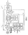
- Integrated ramp sweep fractional frequency synthesizer system 10 includes a conventional frequency synthesizer 14 including a phase frequency detector 16, optional charge pump 18, loop filter 20, fractional divider 22, modulator 24 and VCO 26 which operate in a conventional way.
- phase frequency detector 16 optional charge pump 18, loop filter 20, fractional divider 22, modulator 24 and VCO 26
- Other variations such as programmable integer dividers 27 and 31 and inclusion or exclusion charge pump 18 are also possible.
- the PD 16, R divider 29, optional charge pump 18, fractional divider 22, loop filter 20, VCO 26, or the dividers 27 and 31 may be internal or external to the integrated sweeper.
- fractional divider 22 which divides the VCO frequency output by some number, for the sake of simplicity say 100. That is, fractional divider 22 has a divisor of 100.
- the output from fractional divider 22 is compared in the phase detector (PD) 16 to a reference signal from reference source 28 and optional reference divider 29. If the phase frequency detector 16 detects that VCO 26 output frequency 22b is lower than the reference 28 frequency 29b then PD 16 increases the charge from charge pump 18 to loop filter 20 and loop filter 20 increases the voltage to VCO 26 to drive up its output frequency.
- Charge pump 18 and loop filter 20 may be replaced by an op amp and active filter.
- PD 16 determines that the output of VCO 26 has a higher frequency 22b than reference 28 signal 29b, then PD 16 causes charge pump 18 to lower the charge delivered to loop filter 20 which in turn lowers the voltage to VCO 26 and drops its output frequency. Since frequency synthesizer 14 is a fractional frequency synthesizer there is some means, such as, modulator 24 to cause the fractional effect. This is done conventionally by modulator such as, for example, a ⁇ modulator 24 or similar modulator periodically altering the divisor in fractional divider 22. For example, with a divisor of 100 being applied by divider 22, ⁇ modulator 24 may add a one every ten cycles.
- fractional divider 22 uses a divisor of 100 nine out of ten cycles and on the tenth cycle uses a divider of 101. This causes the average output of fractional output divisor to be no longer 100 but to be 100.1. This is a simplified example with a very rough fractional introduction. In reality, the sequence of VCO divisors generated by the sigma-delta modulator is more complex, in order to achieve the required frequency resolution and to reduce spurious outputs.
- ramp generator 30 is added on the same integrated chip 12 as the modulators 24. and the interface controller 34.
- Ramp generator 30 may be implemented with a ramp controller 30a, look-up table 30b or calculator 30c.
- Calculator 30c may be used to calculate various ramp shapes e.g. exponential, parabolic.
- Look-up table 30b may be used to store many different arbitrary ramp shapes.
- Ramp controller 30a in single mode operation provides the frequency step size, and the number of steps per ramp. The update rate is equal to the PD (16, Fig.1 ) comparison frequency (29b, Fig. 1 ), but may not be limited to it. In an automatic mode the Ramp controller 30a provides those inputs as well as a dwell input.
- the ramp signal thus generated by ramp controller 30a along with ⁇ modulator 24 drives fractional divider 22 to sweep across a range of frequencies which makes the sweep fractional frequency synthesizer useful to generate chirp signals for radar applications and for instrumentation and laboratory equipment, for example.
- Ramp controller 30a may be loaded with the proper step size, number of steps, and driven by an interface, such as, serial/parallel interface (SPI) 34, which receives the input from a host processor on line 36 from a source off-chip.
- SPI serial/parallel interface
- Ramp controller 30a is operated by a trigger on line 38 to enable ramp controller 30a to produce the ramp.
- the ramp controller 30a is configured directly from the host with the ramp parameters (i.e. step size, number of steps, dwell time, ramp points in a look-up table, parameters to calculate a parabolic or other ramp shape, operating mode (int/ext trigger, autorepeat, single-step etc), and, once started, it generates the ramping set-point of the sigma-delta with no other external intervention.
- the ramp controller 30a is implemented as a regular state-machine, and an infinity of particular embodiments can lead to the same functionality.
- the components in dashed box 37 are those essential to be integrated on the chip.
- a typical linear ramp is shown in, Fig. 2 .
- This concept is not limited to any ramp shape, and in its most general form is a look-up table 30b of numbers preloaded by the host processor.
- the improvement is the fact that the frequency updates are located internal to the integrated chip 14, and real time data transfer is not required once the "ramp" starts.
- the positive going edge 40 of a trigger pulse 42 starts an up ramp 44 beginning at starting frequency f 0 and having a number of steps n .
- Each step has a width (T ref ) 46 generated by the signal at 29b and a height 48 as commanded by ramp generator 30 e.g. ramp controller 30a which also sets the number of steps.
- the width 46 and height 48 of the steps define the slope of ramp 44 as well.
- the height 48 of the steps and the number of steps are all provided by ramp controller 30.
- ramp 56 is a down ramp beginning with the first step 58 at frequency f f and continuing for n steps back down to the nth step 60 at frequency f 0 where it rests until the positive going edge 62 of the next trigger pulse 64.
- This is the single mode operation.
- ramp controller 30 provides a dwell time (T dwell ) as indicated at 66 in Fig. 2 . Also in the automatic mode there is only one trigger pulse 42: there are no trigger pulses after that.
- ramp controller 30a automatically starts the ramp with the rising edge 40.
- the programmed dwell period (T dwell ) 66 occurs after which the system automatically begins the second ramp 56 without the application of any more pulses 54, 64.
- This explanation of the single mode and automatic mode operation shows an up ramp 44 followed by a down ramp 56 followed by another up ramp 68 and so on.
- the ramps may be all up ramps, all down ramps or they may start as a down ramp followed by an up ramp, followed by a down ramp, etc.
- the slope when ramping up may not necessarily be equal with the slope when ramping down.
- the system may start with a down ramp beginning at f f ending at f 0 and nearly instantaneously returning to f f and beginning a down ramp again and over and over again.
- the system may provide the mirror image of a down ramp, followed by an up ramp, followed by a down ramp and so on.
- the trigger signal may be hardware originated such as on line 38 or it may be software generated e.g. through SPI 39. Further the trigger may be in single, dual or more complex form for controlling auxiliary mode, one way ramp or two or more ramps or sweeps.
- Ramp parameters are fully programmable through the serial interface 34.
- the synthesized ramp is subject to normal phase lock dynamics. If the loop band width in use is much wider than the rate of the steps, then the locking will be very fast relative to the step rate and the ramp will have a staircase shape. Since the rate of change is the reference frequency, this situation does not typically exist in practice. If the update rate is higher than the loop bandwidth, as is normally the case, then the loop will not fully settle before a new frequency step is received. Hence, after a transient the swept output will follow the set point with a small constant lag and will sweep in a near continuous fashion. Therefore, right after the ramp is triggered, small ramp nonlinearities may appear temporarily at the input.
- the set point of ⁇ modulator 24 is incremented/decremented by a ramp step, in the single mode every reference cycle.
- the start frequency, step size, including width and height, and the number of steps are programmed via the serial interface 34. Note, however, that the integer path and the fractional path passing through the ⁇ transfer function have different delays.
- the integer path which normally is added directly to the modulator sequence at the output of the modulator core, should be artificially delayed to compensate the fractional signal path delay through the modulator. This is shown in Fig. 3 , where modulator 24 includes the modulator core 80, a delay 82, and an adder or summing circuit 84.
- the output from ramp controller 30 includes both an integer and fraction part as indicated on line 86.
- the fractional part goes directly to modulator core 80 whose output is delivered to adder or summer 84; the integer portion, however, goes to delay circuit 82 which may typically delay the integer information for three cycles, for example, to match the delay in modulator core 80.
- the output of delay 82 is then combined with the output from modulator core 80 in adder 84 and provided to fractional divider 22 as explained previously.
Landscapes
- Stabilization Of Oscillater, Synchronisation, Frequency Synthesizers (AREA)
Description
- This application claims benefit of and priority to
U.S. Provisional Application Serial No. 61/126,703, filed May 6, 2008 - This invention relates to an integrated ramp, sweep fractional frequency synthesizer on an integrated circuit chip.
- The ramp generation function can be done using the direct digital synthesis (DDS) technique or using a phase locked loop (PLL) with variable reference frequency or variable voltage controlled oscillator (VCO) division ratio. The DDS approach requires a high performance DAC and smoothing filter, which makes it very difficult to build when high output frequencies and large variations are required.
- Higher output frequencies can be generated using a PLL with a variable reference frequency, which is typically generated with a low frequency DDS, but since the PLL amplifies the spurs generated by the DDS by 20*log(N) - where N is the ratio of the VCO to the reference frequency, the DDS design becomes again very critical.
- The latter approach, using an integrated PLL-based fractional frequency synthesizer with externally controlled VCO division ratio, is prone to introduce digital switching noise and add cost and complexity to the system. In the prior art case where a fractional N synthesizer is used with an external ramp controller, real time transfers of the frequency word are required to the PLL. This is problematic as it causes digital switching noise while the synthesizer is running, and it also uses more power in the inter-chip transactions and costs more than an integrated approach. Also the rate of change of the frequency may be limited by the serial port transfer speed, resulting in a less smooth ramp. One known method to generate a low frequency ramp, or 'chirp', signal is to use an all digital technique using a direct digital synthesizer (DDS), such as that used by Parkes (
US Patent 5,311,193 1994 ). This idea is commonly extended to high frequencies by using the DDS as the reference for an integer PLL using a method such as Gilmore, (US Patent 4,965,533 1990 ). Both the low frequency and the high frequency methods of Parkes and Gilmore rely on a DDS based solution which has problems in that the all digital process can create many unwanted spurious signals when converted back to analog. Also the hardware complexity is significantly larger. Further the idea is restricted as the bandwidth of the PLL should be relatively narrow to reduce the DDS spurs, which creates larger linearity distortions at ramp start or stop. Another method disclosed inGaskel et al. (US 5,079,521 1992 ) uses a fractional synthesizer to generate frequencies of arbitrary values. Another common method to generate a ramped frequency at high carrier frequencies is to directly drive a VCO using a programmable voltage generator based on a high resolution DAC. This approach creates calibration problems due to the non-linear tuning characteristic of the VCO, cannot truly achieve linear frequency sweeps and is generally not suitable for large volume semiconductor manufacturing due to the difficulties in controlling the analog parameters involved in the ramp generation. This is especially true when large sweeps are needed or large temperature variations are encountered. All this prior art is incorporated herein by this reference. EuropeanPatent Application EP 1 858 157 A1 discloses a spread spectrum clock generation system, comprising a digitally controlled Phase Locked Loop (PLL) and a digital frequency profile generator to create near optimal frequency modulation profile for the purpose of achieving spectral flatness in the output frequency modulated clock. - In accordance with various aspects of the subject invention a new integrated ramp, sweep fractional frequency synthesizer is provided which reduces cost of external components, the overhead to control the ramp frequency. This invention provides significant improvement over the DDS approach which is limited in frequency operation, uses large amounts of power, is prone to spurious generation and costs more.
- The invention results from the realization that, in part, an improved sweep fractional frequency synthesizer in various aspects can be achieved by the addition of an integrated ramp generator internal to the fractional frequency synthesizer integrated circuit on a single integrated circuit chip which drives in real time the frequency set-point of the ΔΣ modulator and generates up and/or down frequency ramps with programmable slope (step size and number) and/or dwell for automatic mode operation for repeated ramping whereby autonomous generation of the frequency ramp based on the programmed ramp data is achieved using either an external trigger or an internally self generated trigger to start the ramp.
- The subject invention, however, in other embodiments, need not achieve all these objectives and the claims hereof should not be limited to structures or methods capable of achieving these objectives.
- This invention features an integrated ramp, sweep fractional frequency synthesizer system on an integrated circuit chip including an integrated circuit chip having a fractional frequency synthesizer with a fractional divider responsive to the frequency of a VCO and a modulator for rapidly modifying the divisor of the fractional divider. There is a ramp generator on the same integrated circuit chip which is responsive to a trigger signal to generate a ramp for sweeping the frequency of the fractional frequency synthesizer.
- In preferred embodiments the ramp generator may include a look-up table containing a number of different shaped ramps. The ramp generator may include a ramp controller containing a programmed number of ramp steps and step sizes and being responsive to a trigger signal to generate a ramp shape. The ramp generator may include a calculator circuit for calculating one or more different ramp shapes. The calculator circuit may calculate exponential, parabolic or other ramp shapes. The ramp controller may include a single mode for generating a single ramp upon each trigger signal. The ramp controller may include an automatic mode for enabling repeated ramping upon a single trigger signal and is further programmed with a dwell time to define a repetition period. The on-chip fractional frequency synthesizer may include a loop filter, a charge pump for driving the loop filter and a phase frequency detector, responsive to a reference and the fractional divider, for detecting any deviation between the reference and a VCO driven by the loop filter to develop a compensation signal to enable the loop filter to converge the VCO output with the reference. A serial or parallel interface circuit is provided on the integrated circuit chip for receiving off-chip commands to program the ramp controller. The modulator is a delta-sigma (ΔΣ) type or any other type of fractional fractional modulator. The modulator includes a modulator core responsive to the fractional portion of the ramp controller output and an integer delay path circuit responsive to the integer portion of the ramp controller output to synchronize the integer and fractional outputs from the modulator to the fractional divider. The integer delay path circuit may include a delay circuit responsive to the integer portion of the ramp controller output and a summing circuit for combining the delayed integer portion and the fractional output of the modulator core. The ramp may be a simple ramp extending in a single direction. The ramp may be a compound ramp extending in a number of directions. The ramp may be a compound ramp extending in at least a first direction and a second generally opposite direction. The trigger signal may be hardware generated from an input pin. The trigger signal may be software generated from a serial or parallel interface. The trigger signal may be an auto-mode sweep trigger signal. The trigger signal may be a bi-directional mode sweep trigger signal. The trigger signal may be a single mode sweep trigger signal. The trigger signal may be a dual mode trigger signal.
- This invention also features an integrated fractional modulator, integrated ramp generator and integrated SPI or parallel interface on the same chip, where any of the other synthesizer components may be on or off chip, including the charge pump, phase detector, loop filter, and VCO and where the charge pump is optional if an active loop filter is used.
- Other objects, features and advantages will occur to those skilled in the art from the following description of a preferred embodiment and the accompanying drawings, in which:
-
Fig. 1 is a schematic block diagram of an integrated ramp sweep fractional frequency synthesizer system on an integrated circuit chip according to this invention; -
Fig. 2 illustrates one type of ramp generated by the ramp generator ofFig. 1 ; and -
Fig. 3 is a more detailed schematic diagram of an embodiment of the modulator ofFig. 1 and an optional pre-distortion digital filter. - Aside from the preferred embodiment or embodiments disclosed below, this invention is capable of other embodiments and of being practiced or being carried out in various ways. Thus, it is to be understood that the invention is not limited in its application to the details of construction and the arrangements of components set forth in the following description or illustrated in the drawings. If only one embodiment is described herein, the claims hereof are not to be limited to that embodiment. Moreover, the claims hereof are not to be read restrictively unless there is clear and convincing evidence manifesting a certain exclusion, restriction, or disclaimer.
- The invention is accomplished by adding an integrated controller and ramp circuit both of which are on-chip with the rest of the fractional frequency synthesizer to facilitate the generation of the frequency control ramp based solely on the programmed ramp data and either an external trigger or internally self generated trigger to start the ramp. The ramp, once triggered, automatically provides the required control words to the fractional divider in order to produce a linear or other desired ramp waveform, all of this is integrated with the fractional frequency synthesizer on a single integrated chip and without the further assistance of a DDS or real time data transfers.
- There is shown in
Fig. 1 an integrated ramp, sweep fractionalfrequency synthesizer system 10 on anintegrated circuit chip 12. Integrated ramp sweep fractionalfrequency synthesizer system 10 includes aconventional frequency synthesizer 14 including aphase frequency detector 16,optional charge pump 18,loop filter 20,fractional divider 22,modulator 24 and VCO 26 which operate in a conventional way. Other variations such asprogrammable integer dividers exclusion charge pump 18 are also possible. ThePD 16,R divider 29,optional charge pump 18,fractional divider 22,loop filter 20,VCO 26, or thedividers - In operation the output of
VCO 26 is fed back tofractional divider 22 which divides the VCO frequency output by some number, for the sake of simplicity say 100. That is,fractional divider 22 has a divisor of 100. The output fromfractional divider 22 is compared in the phase detector (PD) 16 to a reference signal fromreference source 28 andoptional reference divider 29. If thephase frequency detector 16 detects thatVCO 26output frequency 22b is lower than thereference 28frequency 29b thenPD 16 increases the charge fromcharge pump 18 toloop filter 20 andloop filter 20 increases the voltage toVCO 26 to drive up its output frequency.Charge pump 18 andloop filter 20 may be replaced by an op amp and active filter. If, on the other hand,PD 16 determines that the output ofVCO 26 has ahigher frequency 22b thanreference 28signal 29b, thenPD 16 causes chargepump 18 to lower the charge delivered toloop filter 20 which in turn lowers the voltage toVCO 26 and drops its output frequency. Sincefrequency synthesizer 14 is a fractional frequency synthesizer there is some means, such as, modulator 24 to cause the fractional effect. This is done conventionally by modulator such as, for example, aΔΣ modulator 24 or similar modulator periodically altering the divisor infractional divider 22. For example, with a divisor of 100 being applied bydivider 22,ΔΣ modulator 24 may add a one every ten cycles. Thusfractional divider 22 uses a divisor of 100 nine out of ten cycles and on the tenth cycle uses a divider of 101. This causes the average output of fractional output divisor to be no longer 100 but to be 100.1. This is a simplified example with a very rough fractional introduction. In reality, the sequence of VCO divisors generated by the sigma-delta modulator is more complex, in order to achieve the required frequency resolution and to reduce spurious outputs. - In accordance with this
invention ramp generator 30 is added on the sameintegrated chip 12 as themodulators 24. and theinterface controller 34.Ramp generator 30 may be implemented with aramp controller 30a, look-up table 30b orcalculator 30c.Calculator 30c may be used to calculate various ramp shapes e.g. exponential, parabolic. Look-up table 30b may be used to store many different arbitrary ramp shapes.Ramp controller 30a in single mode operation provides the frequency step size, and the number of steps per ramp. The update rate is equal to the PD (16,Fig.1 ) comparison frequency (29b,Fig. 1 ), but may not be limited to it. In an automatic mode theRamp controller 30a provides those inputs as well as a dwell input. The ramp signal thus generated byramp controller 30a along withΔΣ modulator 24 drivesfractional divider 22 to sweep across a range of frequencies which makes the sweep fractional frequency synthesizer useful to generate chirp signals for radar applications and for instrumentation and laboratory equipment, for example.Ramp controller 30a may be loaded with the proper step size, number of steps, and driven by an interface, such as, serial/parallel interface (SPI) 34, which receives the input from a host processor online 36 from a source off-chip.Ramp controller 30a is operated by a trigger online 38 to enableramp controller 30a to produce the ramp. - The
ramp controller 30a is configured directly from the host with the ramp parameters (i.e. step size, number of steps, dwell time, ramp points in a look-up table, parameters to calculate a parabolic or other ramp shape, operating mode (int/ext trigger, autorepeat, single-step etc), and, once started, it generates the ramping set-point of the sigma-delta with no other external intervention. Theramp controller 30a is implemented as a regular state-machine, and an infinity of particular embodiments can lead to the same functionality. The components in dashedbox 37 are those essential to be integrated on the chip. - A typical linear ramp is shown in,
Fig. 2 . This concept is not limited to any ramp shape, and in its most general form is a look-up table 30b of numbers preloaded by the host processor. The improvement is the fact that the frequency updates are located internal to theintegrated chip 14, and real time data transfer is not required once the "ramp" starts. In the single mode of operation the positive goingedge 40 of atrigger pulse 42 starts an upramp 44 beginning at starting frequency f0 and having a number of steps n. Each step has a width (Tref) 46 generated by the signal at 29b and aheight 48 as commanded byramp generator 30e.g. ramp controller 30a which also sets the number of steps. Thewidth 46 andheight 48 of the steps define the slope oframp 44 as well. Theheight 48 of the steps and the number of steps are all provided byramp controller 30. When thenth step 50 is reached at frequency ff there are no more steps and the system dwells at the final frequency ff level until the leadingedge 52 of thenext trigger pulse 54. In this example,ramp 56 is a down ramp beginning with thefirst step 58 at frequency ff and continuing for n steps back down to thenth step 60 at frequency f0 where it rests until the positive goingedge 62 of thenext trigger pulse 64. This is the single mode operation. In the automatic modeoperation ramp controller 30 provides a dwell time (Tdwell) as indicated at 66 inFig. 2 . Also in the automatic mode there is only one trigger pulse 42: there are no trigger pulses after that. That is,trigger pulse controller 30a automatically starts the ramp with the risingedge 40. Afterramp 44 reaches thenth step 50 at frequency ff, the programmed dwell period (Tdwell) 66 occurs after which the system automatically begins thesecond ramp 56 without the application of anymore pulses - This explanation of the single mode and automatic mode operation shows an up
ramp 44 followed by adown ramp 56 followed by another upramp 68 and so on. However, this is not a limitation of the invention for either in the single mode or automatic mode of operation the ramps may be all up ramps, all down ramps or they may start as a down ramp followed by an up ramp, followed by a down ramp, etc. Also, the slope when ramping up may not necessarily be equal with the slope when ramping down. For example, in either mode there may be an upramp 44 followed by a rapid return from ff to f0 followed by another up ramp, followed by another rapid return from ff to f0 followed by another up ramp and so on. Or, the system may start with a down ramp beginning at ff ending at f0 and nearly instantaneously returning to ff and beginning a down ramp again and over and over again. And as indicated previously instead of an upramp 44 followed by adown ramp 56, followed by an upramp 68, the system may provide the mirror image of a down ramp, followed by an up ramp, followed by a down ramp and so on. Various triggering schemes may be used forramp generator 30, for example, the trigger signal may be hardware originated such as online 38 or it may be software generated e.g. through SPI 39. Further the trigger may be in single, dual or more complex form for controlling auxiliary mode, one way ramp or two or more ramps or sweeps. - Ramp parameters are fully programmable through the
serial interface 34. However, the synthesized ramp is subject to normal phase lock dynamics. If the loop band width in use is much wider than the rate of the steps, then the locking will be very fast relative to the step rate and the ramp will have a staircase shape. Since the rate of change is the reference frequency, this situation does not typically exist in practice. If the update rate is higher than the loop bandwidth, as is normally the case, then the loop will not fully settle before a new frequency step is received. Hence, after a transient the swept output will follow the set point with a small constant lag and will sweep in a near continuous fashion. Therefore, right after the ramp is triggered, small ramp nonlinearities may appear temporarily at the input. A pre-distortiondigital filter 70,Fig. 3 , may be introduced betweenramp generator 30 andΔΣ modulator 24 to reduce the transient distortion, if necessary. However, since the pre-distortion depends also on the actual external loop filter components, the design of a general pre-distortion digital filter is not trivial. Fortunately, the presence of this filter is not normally needed in practice. A simple practical solution to avoid the start-up transient problem is to start the ramp earlier at a lower frequency (assuming ramping up) and ignore the first part of it. - The set point of
ΔΣ modulator 24 is incremented/decremented by a ramp step, in the single mode every reference cycle. The start frequency, step size, including width and height, and the number of steps are programmed via theserial interface 34. Note, however, that the integer path and the fractional path passing through the ΔΣ transfer function have different delays. The integer path which normally is added directly to the modulator sequence at the output of the modulator core, should be artificially delayed to compensate the fractional signal path delay through the modulator. This is shown inFig. 3 , wheremodulator 24 includes themodulator core 80, adelay 82, and an adder or summingcircuit 84. The output fromramp controller 30 includes both an integer and fraction part as indicated online 86. The fractional part goes directly tomodulator core 80 whose output is delivered to adder orsummer 84; the integer portion, however, goes to delaycircuit 82 which may typically delay the integer information for three cycles, for example, to match the delay inmodulator core 80. The output ofdelay 82 is then combined with the output frommodulator core 80 inadder 84 and provided tofractional divider 22 as explained previously. - Although specific features of the invention are shown in some drawings and not in others, this is for convenience only as each feature may be combined with any or all of the other features in accordance with the invention. The words "including", "comprising", "having", and "with" as used herein are to be interpreted broadly and comprehensively and are not limited to any physical interconnection. Moreover, any embodiments disclosed in the subject application are not to be taken as the only possible embodiments.
- In addition, any amendment presented during the prosecution of the patent application for this patent is not a disclaimer of any claim element presented in the application as filed: those skilled in the art cannot reasonably be expected to draft a claim that would literally encompass all possible equivalents, many equivalents will be unforeseeable at the time of the amendment and are beyond a fair interpretation of what is to be surrendered (if anything), the rationale underlying the amendment may bear no more than a tangential relation to many equivalents, and/or there are many other reasons the applicant can not be expected to describe certain insubstantial substitutes for any claim element amended.
- Other embodiments will occur to those skilled in the art and are within the following claims.
Claims (14)
- A frequency synthesizer system (10) comprising:a fractional divider (22);a modulator (24) of ΔΣ type or other type of fractional modulator, for modifying the divisor of said fractional divider; and a ramp generator (30); said ramp generator (30) being responsive to a trigger signal (38) to generate a ramp for sweeping the frequency of said frequency synthesizer, and an interface circuit (34) responsive to an external controller, to control the ramp generator characterized in that the fractional divider (22), the modulator (24), the ramp generator (30) and the interface circuit (34) are on an integrated circuit chip.
- The frequency synthesizer of claim 1 in which said ramp generator (30) includes a look-up table (30b) containing a number of different shaped ramps.
- The frequency synthesizer of claim 1 in which said ramp generator (30) includes a ramp controller (30a) containing a programmed number of ramp steps and step sizes and being responsive to the trigger signal (38) to generate a ramp shape.
- The frequency synthesizer of claim 1 in which said ramp generator (30) includes a calculator circuit (30c) for calculating one or more different ramp shapes.
- The frequency synthesizer of claim 4 in which said calculator circuit (30c) calculates exponential or parabolic ramp shapes.
- The frequency synthesizer system of claim 3 in which said ramp controller (30a) includes a single mode for generating a ramp upon each trigger signal.
- The frequency synthesizer system of claim 3 in which said ramp controller (30a) includes an automatic mode for enabling repeated ramping upon a single trigger signal and is further programmed with a dwell time to define a repetition period.
- The frequency synthesizer system of claim 1 including a voltage controlled oscillator feedback path comprising a loop filter (20), a charge pump (18) for driving said loop filter (20) and a phase frequency detector (16) for detecting any deviation between a reference frequency and a frequency output by said fractional divider (22) to develop a compensation signal to enable the loop filter to converge the VCO output frequency divided by the fractional divider, said loop filter (20), charge pump (18) and phase frequency detector (16) being on the integrated circuit chip.
- The frequency synthesizer system of claim 4 in which said modulator (24) includes a modulator core (80) responsive to the fractional portion of said ramp controller (30) output and an integer delay path circuit (82) responsive to the integer portion of said ramp controller output to synchronize the integer and fractional outputs from said modulator (24) to said fractional divider (22).
- The frequency synthesizer system of claim 9 in which said integer delay path circuit includes a delay circuit (82) responsive to the integer portion of said ramp controller output and a summing circuit (84) for combining the delayed integer portion and the fractional output of said modulator core.
- The frequency synthesizer system of claim 1 in which said ramp is a linear ramp extending in a single direction.
- The frequency synthesizer system of claim 1 in which said ramp is a compound ramp extending in a first direction and a second generally opposite direction.
- The frequency synthesizer system of claim 1 in which said trigger signal is a bi-directional mode sweep trigger signal.
- The frequency synthesizer system of claim 1 in which said ramp generator (30) has a single step mode where each trigger advances said sweep by one step per trigger.
Applications Claiming Priority (2)
| Application Number | Priority Date | Filing Date | Title |
|---|---|---|---|
| US12670308P | 2008-05-06 | 2008-05-06 | |
| PCT/US2009/002778 WO2009137042A1 (en) | 2008-05-06 | 2009-05-05 | Integrated ramp, sweep fractional frequency synthesizer on an integrated circuit chip |
Publications (3)
| Publication Number | Publication Date |
|---|---|
| EP2283576A1 EP2283576A1 (en) | 2011-02-16 |
| EP2283576A4 EP2283576A4 (en) | 2013-08-14 |
| EP2283576B1 true EP2283576B1 (en) | 2015-10-21 |
Family
ID=41264874
Family Applications (1)
| Application Number | Title | Priority Date | Filing Date |
|---|---|---|---|
| EP09743029.2A Not-in-force EP2283576B1 (en) | 2008-05-06 | 2009-05-05 | Integrated ramp, sweep fractional frequency synthesizer on an integrated circuit chip |
Country Status (5)
| Country | Link |
|---|---|
| US (1) | US8085097B2 (en) |
| EP (1) | EP2283576B1 (en) |
| CN (1) | CN102067453B (en) |
| TW (1) | TWI549434B (en) |
| WO (1) | WO2009137042A1 (en) |
Families Citing this family (23)
| Publication number | Priority date | Publication date | Assignee | Title |
|---|---|---|---|---|
| US8433944B2 (en) | 2010-04-12 | 2013-04-30 | Qualcomm Incorporated | Clock divider system and method with incremental adjustment steps while controlling tolerance in clock duty cycle |
| US8810290B1 (en) * | 2011-01-11 | 2014-08-19 | Hittite Microwave Corporation | Fractional phase locked loop having an exact output frequency and phase and method of using the same |
| US8692594B2 (en) * | 2011-12-19 | 2014-04-08 | Ati Technologies Ulc | Phase-locked loop frequency stepping |
| US9081094B2 (en) | 2012-02-22 | 2015-07-14 | Honeywell International Inc. | Aircraft radar altimeter structure |
| US8866667B2 (en) | 2012-02-22 | 2014-10-21 | Honeywell International Inc. | High sensitivity single antenna FMCW radar |
| US9297885B2 (en) | 2012-07-27 | 2016-03-29 | Honeywell International Inc. | Method of system compensation to reduce the effects of self interference in frequency modulated continuous wave altimeter systems |
| US9194946B1 (en) * | 2012-09-10 | 2015-11-24 | Honeywell International Inc. | Combined FMCW and FM pulse-compression radar systems and methods |
| US9143138B2 (en) | 2013-02-27 | 2015-09-22 | Microsemi Semiconductor Ulc | Phase locked loop frequency synthesizer with reduced jitter |
| US9020089B2 (en) * | 2013-07-12 | 2015-04-28 | Infineon Technologies Ag | Phase-locked loop (PLL)-based frequency synthesizer |
| CN104378116B (en) * | 2013-08-14 | 2018-03-16 | 颜至远 | DAC-circuit device with micro pulse wave absorption function |
| KR101465370B1 (en) * | 2013-12-09 | 2014-11-26 | 한국항공우주연구원 | Apparatus and method of generating of direct digital synthesizer chirp signal using phase accumulation polynomial |
| EP2903163B1 (en) * | 2014-02-04 | 2019-08-21 | Hittite Microwave LLC | Apparatus and methods for fast charge pump holdover on signal interruption |
| CN103840824A (en) * | 2014-03-10 | 2014-06-04 | 南京软仪测试技术有限公司 | Frequency synthesis signal device capable of improving frequency resolution, and synthesis method of frequency synthesis signal device |
| US9660605B2 (en) | 2014-06-12 | 2017-05-23 | Honeywell International Inc. | Variable delay line using variable capacitors in a maximally flat time delay filter |
| US10018716B2 (en) | 2014-06-26 | 2018-07-10 | Honeywell International Inc. | Systems and methods for calibration and optimization of frequency modulated continuous wave radar altimeters using adjustable self-interference cancellation |
| CN104124966B (en) * | 2014-07-21 | 2017-07-14 | 中国电子科技集团公司第四十一研究所 | A kind of Direct frequency synthesizer method for producing linear FM signal |
| US10725150B2 (en) * | 2014-12-23 | 2020-07-28 | Infineon Technologies Ag | System and method for radar |
| US9397675B1 (en) * | 2015-07-31 | 2016-07-19 | Shure Acquisition Holdings, Inc. | Hybrid frequency synthesizer and method |
| EP3208579B1 (en) * | 2016-02-22 | 2020-01-29 | VEGA Grieshaber KG | Reduction of power spikes in the average power range of fill level measuring devices |
| US12017919B2 (en) * | 2017-11-03 | 2024-06-25 | The Regents Of The University Of California | Orientation independent, room temperature, hyperpolarization of diamond nano- and micro-particles |
| EP3579012B1 (en) | 2018-06-06 | 2022-03-30 | NXP USA, Inc. | Phase preset for fast chirp pll |
| EP3579011B1 (en) | 2018-06-06 | 2022-03-16 | NXP USA, Inc. | Boosted return time for fast chirp pll and calibration method |
| KR20230079723A (en) * | 2021-11-29 | 2023-06-07 | 삼성전자주식회사 | Fractional divider with phase shifter and fractional phase locked loop including the same |
Citations (1)
| Publication number | Priority date | Publication date | Assignee | Title |
|---|---|---|---|---|
| US6091356A (en) * | 1998-10-05 | 2000-07-18 | Sensor Concepts Incorporated | Chirp source with rolling frequency lock for generating linear frequency chirps |
Family Cites Families (19)
| Publication number | Priority date | Publication date | Assignee | Title |
|---|---|---|---|---|
| US4038689A (en) * | 1976-06-14 | 1977-07-26 | Matsushita Electric Corporation Of America | Frequency synthesizer tuning system with manual fine tuning control |
| US4965533A (en) * | 1989-08-31 | 1990-10-23 | Qualcomm, Inc. | Direct digital synthesizer driven phase lock loop frequency synthesizer |
| US5023571A (en) * | 1989-09-29 | 1991-06-11 | Hewlett-Packard Company | Digitally-synchronized sweep signal source |
| GB2238434B (en) * | 1989-11-22 | 1994-03-16 | Stc Plc | Frequency synthesiser |
| GB2248355B (en) * | 1990-09-26 | 1994-07-13 | British Aerospace | Digital chirp generator |
| WO1995020269A1 (en) * | 1994-01-24 | 1995-07-27 | BALDWIN, Douglas, R. | Adjustable frequency synthesizer |
| US6047029A (en) * | 1997-09-16 | 2000-04-04 | Telefonaktiebolaget Lm Ericsson | Post-filtered delta sigma for controlling a phase locked loop modulator |
| US5986512A (en) * | 1997-12-12 | 1999-11-16 | Telefonaktiebolaget L M Ericsson (Publ) | Σ-Δ modulator-controlled phase-locked-loop circuit |
| FI107478B (en) * | 1999-12-03 | 2001-08-15 | Nokia Networks Oy | Digital ramp generator with power output control |
| US6931243B2 (en) * | 2001-12-21 | 2005-08-16 | Texas Instruments Incorporated | Fully integrated low noise multi-loop synthesizer with fine frequency resolution for HDD read channel and RF wireless local oscillator applications |
| US6975848B2 (en) * | 2002-06-04 | 2005-12-13 | Parkervision, Inc. | Method and apparatus for DC offset removal in a radio frequency communication channel |
| JP2004104228A (en) * | 2002-09-05 | 2004-04-02 | Matsushita Electric Ind Co Ltd | Signal processing device and signal processing method, delta-sigma modulation type fractional frequency division PLL frequency synthesizer, wireless communication device, delta-sigma modulation type D / A converter |
| JP4064338B2 (en) * | 2003-12-10 | 2008-03-19 | 松下電器産業株式会社 | Delta-sigma fractional frequency division PLL synthesizer |
| US7356312B2 (en) * | 2004-03-05 | 2008-04-08 | Telefonaktiebolaget Lm Ericsson (Publ) | Fractional frequency synthesizer |
| US7529789B2 (en) * | 2004-11-01 | 2009-05-05 | Metanoia Technologies, Inc. | Method for representing complex numbers in a communication system |
| US7098754B2 (en) * | 2005-01-31 | 2006-08-29 | Rf Micro Devices, Inc. | Fractional-N offset phase locked loop |
| JP2007134928A (en) * | 2005-11-10 | 2007-05-31 | Renesas Technology Corp | Rf analog signal processing unit and mobile terminal device with mounted signal processing unit |
| JP2007259122A (en) * | 2006-03-23 | 2007-10-04 | Renesas Technology Corp | Semiconductor integrated circuit for communication |
| US8037336B2 (en) * | 2006-05-15 | 2011-10-11 | Stmicroelectronics Pvt, Ltd. | Spread spectrum clock generation |
-
2009
- 2009-05-04 US US12/387,529 patent/US8085097B2/en not_active Expired - Fee Related
- 2009-05-05 EP EP09743029.2A patent/EP2283576B1/en not_active Not-in-force
- 2009-05-05 WO PCT/US2009/002778 patent/WO2009137042A1/en not_active Ceased
- 2009-05-05 CN CN200980122499.0A patent/CN102067453B/en not_active Expired - Fee Related
- 2009-05-06 TW TW098115032A patent/TWI549434B/en active
Patent Citations (1)
| Publication number | Priority date | Publication date | Assignee | Title |
|---|---|---|---|---|
| US6091356A (en) * | 1998-10-05 | 2000-07-18 | Sensor Concepts Incorporated | Chirp source with rolling frequency lock for generating linear frequency chirps |
Also Published As
| Publication number | Publication date |
|---|---|
| TWI549434B (en) | 2016-09-11 |
| US8085097B2 (en) | 2011-12-27 |
| WO2009137042A1 (en) | 2009-11-12 |
| CN102067453B (en) | 2015-05-20 |
| US20090278611A1 (en) | 2009-11-12 |
| EP2283576A1 (en) | 2011-02-16 |
| EP2283576A4 (en) | 2013-08-14 |
| TW200952343A (en) | 2009-12-16 |
| CN102067453A (en) | 2011-05-18 |
Similar Documents
| Publication | Publication Date | Title |
|---|---|---|
| US8085097B2 (en) | Integrated ramp, sweep fractional frequency synthesizer on an integrated circuit chip | |
| EP3618281B1 (en) | Parallel fractional-n phase locked loop circuit | |
| US8994420B2 (en) | Higher-order phase noise modulator to reduce spurs and quantization noise | |
| CN110048714B (en) | Synthesizer and Phase Frequency Detector | |
| CN1190931C (en) | Radio transmitter architecture comprising PLL and delta-sigma modulator | |
| US7899422B1 (en) | Sigma delta modulated phase lock loop with phase interpolation | |
| US6414555B2 (en) | Frequency synthesizer | |
| US6509800B2 (en) | Polyphase noise-shaping fractional-N frequency synthesizer | |
| US9219487B1 (en) | Frequency ramp generation in PLL based RF frontend | |
| US4114110A (en) | Frequency synthesizer | |
| US8587352B2 (en) | Fractional-N phase locked loop | |
| US9280928B2 (en) | Apparatus and method for driving LED display | |
| JP6494888B2 (en) | PLL circuit | |
| US6943598B2 (en) | Reduced-size integrated phase-locked loop | |
| US7579886B2 (en) | Phase locked loop with adaptive phase error compensation | |
| US7327820B2 (en) | Method and apparatus for reducing quantization noise in fractional-N frequency synthesizers | |
| US6700447B1 (en) | Trimming of a two point phase modulator | |
| US20110140790A1 (en) | Frequency synthesizers | |
| US7298218B2 (en) | Frequency synthesizer architecture | |
| KR101307498B1 (en) | Sigma-delta based phase lock loop | |
| US7196587B2 (en) | Waveform lineariser | |
| EP2890013A1 (en) | Phase locked loop and control method thereof | |
| US20140184274A1 (en) | Fractional-n frequency synthesizer with low quantization noise | |
| US7649428B2 (en) | Method and system for generating noise in a frequency synthesizer | |
| US20060159157A1 (en) | Digital spread spectrum clock signal generation |
Legal Events
| Date | Code | Title | Description |
|---|---|---|---|
| PUAI | Public reference made under article 153(3) epc to a published international application that has entered the european phase |
Free format text: ORIGINAL CODE: 0009012 |
|
| 17P | Request for examination filed |
Effective date: 20101102 |
|
| AK | Designated contracting states |
Kind code of ref document: A1 Designated state(s): AT BE BG CH CY CZ DE DK EE ES FI FR GB GR HR HU IE IS IT LI LT LU LV MC MK MT NL NO PL PT RO SE SI SK TR |
|
| AX | Request for extension of the european patent |
Extension state: AL BA RS |
|
| DAX | Request for extension of the european patent (deleted) | ||
| A4 | Supplementary search report drawn up and despatched |
Effective date: 20130717 |
|
| RIC1 | Information provided on ipc code assigned before grant |
Ipc: H03L 7/06 20060101AFI20130711BHEP |
|
| 17Q | First examination report despatched |
Effective date: 20131105 |
|
| GRAP | Despatch of communication of intention to grant a patent |
Free format text: ORIGINAL CODE: EPIDOSNIGR1 |
|
| GRAJ | Information related to disapproval of communication of intention to grant by the applicant or resumption of examination proceedings by the epo deleted |
Free format text: ORIGINAL CODE: EPIDOSDIGR1 |
|
| GRAP | Despatch of communication of intention to grant a patent |
Free format text: ORIGINAL CODE: EPIDOSNIGR1 |
|
| RIN1 | Information on inventor provided before grant (corrected) |
Inventor name: LIPAN, TUDOR Inventor name: CLOUTIER, MARK, MILES |
|
| INTG | Intention to grant announced |
Effective date: 20141118 |
|
| INTG | Intention to grant announced |
Effective date: 20141128 |
|
| GRAS | Grant fee paid |
Free format text: ORIGINAL CODE: EPIDOSNIGR3 |
|
| GRAP | Despatch of communication of intention to grant a patent |
Free format text: ORIGINAL CODE: EPIDOSNIGR1 |
|
| INTG | Intention to grant announced |
Effective date: 20150625 |
|
| GRAA | (expected) grant |
Free format text: ORIGINAL CODE: 0009210 |
|
| AK | Designated contracting states |
Kind code of ref document: B1 Designated state(s): AT BE BG CH CY CZ DE DK EE ES FI FR GB GR HR HU IE IS IT LI LT LU LV MC MK MT NL NO PL PT RO SE SI SK TR |
|
| REG | Reference to a national code |
Ref country code: GB Ref legal event code: FG4D Ref country code: NL Ref legal event code: MP Effective date: 20151021 |
|
| REG | Reference to a national code |
Ref country code: CH Ref legal event code: EP |
|
| REG | Reference to a national code |
Ref country code: AT Ref legal event code: REF Ref document number: 757175 Country of ref document: AT Kind code of ref document: T Effective date: 20151115 |
|
| REG | Reference to a national code |
Ref country code: IE Ref legal event code: FG4D |
|
| REG | Reference to a national code |
Ref country code: DE Ref legal event code: R096 Ref document number: 602009034355 Country of ref document: DE |
|
| REG | Reference to a national code |
Ref country code: LT Ref legal event code: MG4D |
|
| REG | Reference to a national code |
Ref country code: AT Ref legal event code: MK05 Ref document number: 757175 Country of ref document: AT Kind code of ref document: T Effective date: 20151021 |
|
| PG25 | Lapsed in a contracting state [announced via postgrant information from national office to epo] |
Ref country code: NL Free format text: LAPSE BECAUSE OF FAILURE TO SUBMIT A TRANSLATION OF THE DESCRIPTION OR TO PAY THE FEE WITHIN THE PRESCRIBED TIME-LIMIT Effective date: 20151021 Ref country code: HR Free format text: LAPSE BECAUSE OF FAILURE TO SUBMIT A TRANSLATION OF THE DESCRIPTION OR TO PAY THE FEE WITHIN THE PRESCRIBED TIME-LIMIT Effective date: 20151021 Ref country code: ES Free format text: LAPSE BECAUSE OF FAILURE TO SUBMIT A TRANSLATION OF THE DESCRIPTION OR TO PAY THE FEE WITHIN THE PRESCRIBED TIME-LIMIT Effective date: 20151021 Ref country code: IS Free format text: LAPSE BECAUSE OF FAILURE TO SUBMIT A TRANSLATION OF THE DESCRIPTION OR TO PAY THE FEE WITHIN THE PRESCRIBED TIME-LIMIT Effective date: 20160221 Ref country code: IT Free format text: LAPSE BECAUSE OF FAILURE TO SUBMIT A TRANSLATION OF THE DESCRIPTION OR TO PAY THE FEE WITHIN THE PRESCRIBED TIME-LIMIT Effective date: 20151021 Ref country code: NO Free format text: LAPSE BECAUSE OF FAILURE TO SUBMIT A TRANSLATION OF THE DESCRIPTION OR TO PAY THE FEE WITHIN THE PRESCRIBED TIME-LIMIT Effective date: 20160121 Ref country code: LT Free format text: LAPSE BECAUSE OF FAILURE TO SUBMIT A TRANSLATION OF THE DESCRIPTION OR TO PAY THE FEE WITHIN THE PRESCRIBED TIME-LIMIT Effective date: 20151021 |
|
| PG25 | Lapsed in a contracting state [announced via postgrant information from national office to epo] |
Ref country code: GR Free format text: LAPSE BECAUSE OF FAILURE TO SUBMIT A TRANSLATION OF THE DESCRIPTION OR TO PAY THE FEE WITHIN THE PRESCRIBED TIME-LIMIT Effective date: 20160122 Ref country code: PT Free format text: LAPSE BECAUSE OF FAILURE TO SUBMIT A TRANSLATION OF THE DESCRIPTION OR TO PAY THE FEE WITHIN THE PRESCRIBED TIME-LIMIT Effective date: 20160222 Ref country code: PL Free format text: LAPSE BECAUSE OF FAILURE TO SUBMIT A TRANSLATION OF THE DESCRIPTION OR TO PAY THE FEE WITHIN THE PRESCRIBED TIME-LIMIT Effective date: 20151021 Ref country code: AT Free format text: LAPSE BECAUSE OF FAILURE TO SUBMIT A TRANSLATION OF THE DESCRIPTION OR TO PAY THE FEE WITHIN THE PRESCRIBED TIME-LIMIT Effective date: 20151021 Ref country code: LV Free format text: LAPSE BECAUSE OF FAILURE TO SUBMIT A TRANSLATION OF THE DESCRIPTION OR TO PAY THE FEE WITHIN THE PRESCRIBED TIME-LIMIT Effective date: 20151021 Ref country code: FI Free format text: LAPSE BECAUSE OF FAILURE TO SUBMIT A TRANSLATION OF THE DESCRIPTION OR TO PAY THE FEE WITHIN THE PRESCRIBED TIME-LIMIT Effective date: 20151021 Ref country code: SE Free format text: LAPSE BECAUSE OF FAILURE TO SUBMIT A TRANSLATION OF THE DESCRIPTION OR TO PAY THE FEE WITHIN THE PRESCRIBED TIME-LIMIT Effective date: 20151021 |
|
| REG | Reference to a national code |
Ref country code: DE Ref legal event code: R082 Ref document number: 602009034355 Country of ref document: DE Representative=s name: WINTER, BRANDL - PARTNERSCHAFT MBB, PATENTANWA, DE Ref country code: DE Ref legal event code: R082 Ref document number: 602009034355 Country of ref document: DE Representative=s name: WINTER, BRANDL, FUERNISS, HUEBNER, ROESS, KAIS, DE Ref country code: DE Ref legal event code: R081 Ref document number: 602009034355 Country of ref document: DE Owner name: HITTITE MICROWAVE LLC, CHELMSFORD, US Free format text: FORMER OWNER: HITTITE MICROWAVE CORPORATION, CHELMSFORD, MASS., US |
|
| REG | Reference to a national code |
Ref country code: DE Ref legal event code: R097 Ref document number: 602009034355 Country of ref document: DE |
|
| PG25 | Lapsed in a contracting state [announced via postgrant information from national office to epo] |
Ref country code: CZ Free format text: LAPSE BECAUSE OF FAILURE TO SUBMIT A TRANSLATION OF THE DESCRIPTION OR TO PAY THE FEE WITHIN THE PRESCRIBED TIME-LIMIT Effective date: 20151021 |
|
| RAP2 | Party data changed (patent owner data changed or rights of a patent transferred) |
Owner name: HITTITE MICROWAVE LLC |
|
| PLBE | No opposition filed within time limit |
Free format text: ORIGINAL CODE: 0009261 |
|
| STAA | Information on the status of an ep patent application or granted ep patent |
Free format text: STATUS: NO OPPOSITION FILED WITHIN TIME LIMIT |
|
| PG25 | Lapsed in a contracting state [announced via postgrant information from national office to epo] |
Ref country code: SK Free format text: LAPSE BECAUSE OF FAILURE TO SUBMIT A TRANSLATION OF THE DESCRIPTION OR TO PAY THE FEE WITHIN THE PRESCRIBED TIME-LIMIT Effective date: 20151021 Ref country code: BE Free format text: LAPSE BECAUSE OF NON-PAYMENT OF DUE FEES Effective date: 20160531 Ref country code: RO Free format text: LAPSE BECAUSE OF FAILURE TO SUBMIT A TRANSLATION OF THE DESCRIPTION OR TO PAY THE FEE WITHIN THE PRESCRIBED TIME-LIMIT Effective date: 20151021 Ref country code: DK Free format text: LAPSE BECAUSE OF FAILURE TO SUBMIT A TRANSLATION OF THE DESCRIPTION OR TO PAY THE FEE WITHIN THE PRESCRIBED TIME-LIMIT Effective date: 20151021 Ref country code: EE Free format text: LAPSE BECAUSE OF FAILURE TO SUBMIT A TRANSLATION OF THE DESCRIPTION OR TO PAY THE FEE WITHIN THE PRESCRIBED TIME-LIMIT Effective date: 20151021 |
|
| 26N | No opposition filed |
Effective date: 20160722 |
|
| PG25 | Lapsed in a contracting state [announced via postgrant information from national office to epo] |
Ref country code: SI Free format text: LAPSE BECAUSE OF FAILURE TO SUBMIT A TRANSLATION OF THE DESCRIPTION OR TO PAY THE FEE WITHIN THE PRESCRIBED TIME-LIMIT Effective date: 20151021 |
|
| PG25 | Lapsed in a contracting state [announced via postgrant information from national office to epo] |
Ref country code: LU Free format text: LAPSE BECAUSE OF FAILURE TO SUBMIT A TRANSLATION OF THE DESCRIPTION OR TO PAY THE FEE WITHIN THE PRESCRIBED TIME-LIMIT Effective date: 20160505 Ref country code: BE Free format text: LAPSE BECAUSE OF FAILURE TO SUBMIT A TRANSLATION OF THE DESCRIPTION OR TO PAY THE FEE WITHIN THE PRESCRIBED TIME-LIMIT Effective date: 20151021 |
|
| REG | Reference to a national code |
Ref country code: CH Ref legal event code: PL |
|
| PG25 | Lapsed in a contracting state [announced via postgrant information from national office to epo] |
Ref country code: CH Free format text: LAPSE BECAUSE OF NON-PAYMENT OF DUE FEES Effective date: 20160531 Ref country code: LI Free format text: LAPSE BECAUSE OF NON-PAYMENT OF DUE FEES Effective date: 20160531 |
|
| REG | Reference to a national code |
Ref country code: IE Ref legal event code: MM4A |
|
| REG | Reference to a national code |
Ref country code: FR Ref legal event code: ST Effective date: 20170131 |
|
| PG25 | Lapsed in a contracting state [announced via postgrant information from national office to epo] |
Ref country code: FR Free format text: LAPSE BECAUSE OF NON-PAYMENT OF DUE FEES Effective date: 20160531 |
|
| PG25 | Lapsed in a contracting state [announced via postgrant information from national office to epo] |
Ref country code: IE Free format text: LAPSE BECAUSE OF NON-PAYMENT OF DUE FEES Effective date: 20160505 |
|
| PG25 | Lapsed in a contracting state [announced via postgrant information from national office to epo] |
Ref country code: HU Free format text: LAPSE BECAUSE OF FAILURE TO SUBMIT A TRANSLATION OF THE DESCRIPTION OR TO PAY THE FEE WITHIN THE PRESCRIBED TIME-LIMIT; INVALID AB INITIO Effective date: 20090505 Ref country code: CY Free format text: LAPSE BECAUSE OF FAILURE TO SUBMIT A TRANSLATION OF THE DESCRIPTION OR TO PAY THE FEE WITHIN THE PRESCRIBED TIME-LIMIT Effective date: 20151021 |
|
| PG25 | Lapsed in a contracting state [announced via postgrant information from national office to epo] |
Ref country code: MT Free format text: LAPSE BECAUSE OF NON-PAYMENT OF DUE FEES Effective date: 20160531 Ref country code: TR Free format text: LAPSE BECAUSE OF FAILURE TO SUBMIT A TRANSLATION OF THE DESCRIPTION OR TO PAY THE FEE WITHIN THE PRESCRIBED TIME-LIMIT Effective date: 20151021 Ref country code: MK Free format text: LAPSE BECAUSE OF FAILURE TO SUBMIT A TRANSLATION OF THE DESCRIPTION OR TO PAY THE FEE WITHIN THE PRESCRIBED TIME-LIMIT Effective date: 20151021 Ref country code: MC Free format text: LAPSE BECAUSE OF FAILURE TO SUBMIT A TRANSLATION OF THE DESCRIPTION OR TO PAY THE FEE WITHIN THE PRESCRIBED TIME-LIMIT Effective date: 20151021 |
|
| PG25 | Lapsed in a contracting state [announced via postgrant information from national office to epo] |
Ref country code: BG Free format text: LAPSE BECAUSE OF FAILURE TO SUBMIT A TRANSLATION OF THE DESCRIPTION OR TO PAY THE FEE WITHIN THE PRESCRIBED TIME-LIMIT Effective date: 20151021 |
|
| PGFP | Annual fee paid to national office [announced via postgrant information from national office to epo] |
Ref country code: DE Payment date: 20230419 Year of fee payment: 15 |
|
| PGFP | Annual fee paid to national office [announced via postgrant information from national office to epo] |
Ref country code: GB Payment date: 20230420 Year of fee payment: 15 |
|
| REG | Reference to a national code |
Ref country code: DE Ref legal event code: R119 Ref document number: 602009034355 Country of ref document: DE |
|
| GBPC | Gb: european patent ceased through non-payment of renewal fee |
Effective date: 20240505 |
|
| PG25 | Lapsed in a contracting state [announced via postgrant information from national office to epo] |
Ref country code: DE Free format text: LAPSE BECAUSE OF NON-PAYMENT OF DUE FEES Effective date: 20241203 |
|
| PG25 | Lapsed in a contracting state [announced via postgrant information from national office to epo] |
Ref country code: GB Free format text: LAPSE BECAUSE OF NON-PAYMENT OF DUE FEES Effective date: 20240505 |