EP2283517B1 - Integrated circuit manufacturing method and integrated circuit - Google Patents
Integrated circuit manufacturing method and integrated circuit Download PDFInfo
- Publication number
- EP2283517B1 EP2283517B1 EP09754245.0A EP09754245A EP2283517B1 EP 2283517 B1 EP2283517 B1 EP 2283517B1 EP 09754245 A EP09754245 A EP 09754245A EP 2283517 B1 EP2283517 B1 EP 2283517B1
- Authority
- EP
- European Patent Office
- Prior art keywords
- layer
- over
- dielectric material
- forming
- trenches
- Prior art date
- Legal status (The legal status is an assumption and is not a legal conclusion. Google has not performed a legal analysis and makes no representation as to the accuracy of the status listed.)
- Not-in-force
Links
Images



Classifications
-
- H—ELECTRICITY
- H10—SEMICONDUCTOR DEVICES; ELECTRIC SOLID-STATE DEVICES NOT OTHERWISE PROVIDED FOR
- H10W—GENERIC PACKAGES, INTERCONNECTIONS, CONNECTORS OR OTHER CONSTRUCTIONAL DETAILS OF DEVICES COVERED BY CLASS H10
- H10W20/00—Interconnections in chips, wafers or substrates
- H10W20/01—Manufacture or treatment
- H10W20/071—Manufacture or treatment of dielectric parts thereof
- H10W20/072—Manufacture or treatment of dielectric parts thereof of dielectric parts comprising air gaps
-
- H—ELECTRICITY
- H10—SEMICONDUCTOR DEVICES; ELECTRIC SOLID-STATE DEVICES NOT OTHERWISE PROVIDED FOR
- H10W—GENERIC PACKAGES, INTERCONNECTIONS, CONNECTORS OR OTHER CONSTRUCTIONAL DETAILS OF DEVICES COVERED BY CLASS H10
- H10W20/00—Interconnections in chips, wafers or substrates
- H10W20/40—Interconnections external to wafers or substrates, e.g. back-end-of-line [BEOL] metallisations or vias connecting to gate electrodes
- H10W20/45—Interconnections external to wafers or substrates, e.g. back-end-of-line [BEOL] metallisations or vias connecting to gate electrodes characterised by their insulating parts
- H10W20/46—Interconnections external to wafers or substrates, e.g. back-end-of-line [BEOL] metallisations or vias connecting to gate electrodes characterised by their insulating parts comprising air gaps
-
- H—ELECTRICITY
- H10—SEMICONDUCTOR DEVICES; ELECTRIC SOLID-STATE DEVICES NOT OTHERWISE PROVIDED FOR
- H10W—GENERIC PACKAGES, INTERCONNECTIONS, CONNECTORS OR OTHER CONSTRUCTIONAL DETAILS OF DEVICES COVERED BY CLASS H10
- H10W72/00—Interconnections or connectors in packages
- H10W72/01—Manufacture or treatment
- H10W72/019—Manufacture or treatment of bond pads
-
- H—ELECTRICITY
- H10—SEMICONDUCTOR DEVICES; ELECTRIC SOLID-STATE DEVICES NOT OTHERWISE PROVIDED FOR
- H10W—GENERIC PACKAGES, INTERCONNECTIONS, CONNECTORS OR OTHER CONSTRUCTIONAL DETAILS OF DEVICES COVERED BY CLASS H10
- H10W72/00—Interconnections or connectors in packages
- H10W72/90—Bond pads, in general
- H10W72/921—Structures or relative sizes of bond pads
- H10W72/923—Bond pads having multiple stacked layers
-
- H—ELECTRICITY
- H10—SEMICONDUCTOR DEVICES; ELECTRIC SOLID-STATE DEVICES NOT OTHERWISE PROVIDED FOR
- H10W—GENERIC PACKAGES, INTERCONNECTIONS, CONNECTORS OR OTHER CONSTRUCTIONAL DETAILS OF DEVICES COVERED BY CLASS H10
- H10W72/00—Interconnections or connectors in packages
- H10W72/90—Bond pads, in general
- H10W72/931—Shapes of bond pads
- H10W72/934—Cross-sectional shape, i.e. in side view
-
- H—ELECTRICITY
- H10—SEMICONDUCTOR DEVICES; ELECTRIC SOLID-STATE DEVICES NOT OTHERWISE PROVIDED FOR
- H10W—GENERIC PACKAGES, INTERCONNECTIONS, CONNECTORS OR OTHER CONSTRUCTIONAL DETAILS OF DEVICES COVERED BY CLASS H10
- H10W72/00—Interconnections or connectors in packages
- H10W72/90—Bond pads, in general
- H10W72/941—Dispositions of bond pads
- H10W72/9415—Dispositions of bond pads relative to the surface, e.g. recessed, protruding
-
- H—ELECTRICITY
- H10—SEMICONDUCTOR DEVICES; ELECTRIC SOLID-STATE DEVICES NOT OTHERWISE PROVIDED FOR
- H10W—GENERIC PACKAGES, INTERCONNECTIONS, CONNECTORS OR OTHER CONSTRUCTIONAL DETAILS OF DEVICES COVERED BY CLASS H10
- H10W72/00—Interconnections or connectors in packages
- H10W72/90—Bond pads, in general
- H10W72/951—Materials of bond pads
- H10W72/952—Materials of bond pads comprising metals or metalloids, e.g. PbSn, Ag or Cu
Definitions
- the present invention relates to a method of manufacturing an integrated circuit (IC) comprising providing a substrate stack carrying a first layer comprising conductive regions and forming a interconnect layer over the first layer, said interconnect layer comprising a portion to be oriented between a bond pad and the substrate stack.
- IC integrated circuit
- the present invention further relates to an IC comprising a bond pad; a substrate stack carrying a first layer comprising conductive regions; and a layer of a dielectric material over the first layer, said dielectric material comprising a portion between the bond pad and the substrate stack.
- Fig. 1 shows a cross-section of an integrated circuit.
- the substrate 100 which typically includes the semiconductor devices such as transistors, diodes and so on, is covered by a number of interconnect layers 120, each comprising patterned metal portions 125 separated by a suitable dielectric material.
- the interconnect layers 120 are typically separated by via layers 130, including vias 135 that interconnect metal portions 125 in different interconnect layers 120.
- the uppermost interconnect layer 140 is the interconnect layer that is closest to the bond pads 160 of the IC, which are typically embedded in a passivation layer 150.
- the uppermost interconnect layer 140 has a dielectric material portion 145 located underneath the bond pad 160.
- the bond pad 160 is shown with a metal cap 170.
- the mechanical forces on the bond pad 160 to ensure a good connection between the bond pad 160 and a wire can cause damage to the dielectric material portion 145, e.g. delamination, cracking or even collapse of the interconnect layer 140. Similar mechanical forces may for instance be experienced during some packaging steps, e.g. molding. Such damage is likely to cause electrical failures within the IC at some point during its lifetime. For this reason, relatively brittle low-k materials are avoided in the uppermost interconnect layers of an IC. However, even more robust dielectric materials, e.g. SiO 2 , can still suffer damage when exposed to such mechanical forces.
- FIG. 2 shows a cross-section of another IC design.
- the area 245 of the interconnect layer 140 under the bond pad 160 is filled with metal interconnect portions to ensure that the metal, which typically is more rigid than the dielectric material in the interconnect layer 140 in between the metal portions, absorbs most of the pressure forces exerted on the IC during subsequent process steps.
- the introduction of such a design rule significantly reduces the flexibility of the interconnect design, which may prohibit the adequate routing of the required interconnections in the design stage of the IC.
- US 2004/0245637 describes a method for forming interlevel dielectric levels in a multilevel interconnect structure formed by a damsine process.
- US2004/222533 describes a semiconductor device which includes a foundation having a first conductive region, and an interconnection layer provided separate from the foundation. A first region occupying a range from the foundation to the interconnection layer is filled with gas or provided with a first interlayer dielectric film.
- An embodiment of the invention can provide a method of manufacturing an IC having improved structural integrity.
- An embodiment of the invention can provide an IC having improved structural integrity.
- a method of manufacturing an integrated circuit comprising:
- a portion of a dielectric material in an interconnect layer underneath a bond pad is patterned such that a plurality of air gaps are formed, thereby defining one or more pillars of the dielectric material underneath the bond pad area.
- the pillars provide structural support for preventing damage to the interconnect layer under pressure exerted on the bond pad.
- the first layer may be a metal layer, which may be patterned.
- the formation of pillars of the dielectric material under the bond pad improves the elastical flexibility of the portion of the interconnect layer under the bond pad compared to a continuous dielectric material portion as shown in Fig. 1 . So even though less dielectric material may be present under the bond pad, the resilience of the interconnect layer is nevertheless improved.
- the dielectric material may be chosen to be any material that has a high enough density to withstand the mechanical forces exerted e.g. during the wire-bonding process, e.g. silicon oxide or a dense low-k material.
- the introduction of the air-filled trenches has the additional advantage that the dielectric constant of the dielectric material has become less critical because the air-filled trenches help to reduce the capacitive coupling between neighboring metal tracks. This enables the choice of dielectric materials for the uppermost interconnect layer that would not have been considered previously because of the performance issues associated with the capacitive coupling between neighboring metal portions in this interconnect layer.
- the dielectric material may be used in combination with a fluorosilicate glass for the via layers, which further improves the structural integrity of the IC.
- the trenches may be formed by forming a hard mask over the interconnect layer; depositing a resist over the hard mask; patterning the resist; and etching the plurality of trenches.
- the resist may be removed after said etching step. Any suitable hard mask and resist material may be used.
- the trenches may be filled by depositing the thermally degradable polymer over the interconnect layer, thereby filling said trenches; and subsequently removing excess thermally degradable polymer. Any suitable deposition technique such as spin-coating may be used.
- the method further comprises forming, in said portion, at least one further trench over at least one of said regions following said filling step, and wherein forming the further layer comprising forming a further metal layer over the interconnect layer, said forming step including filling the at least one further trench with the further metal.
- the portion underneath the bond pad comprises both air-filled trenches and metal-filled, e.g. copper-filled trenches, with the air-filled trenches typically located between a pair of metal-filled trenches, with at least one of said metal-filled trenches being located in said portion.
- the at least one further trench may be formed by depositing a further hard mask over the interconnect layer; depositing a further resist over the further hard mask; patterning the further resist; and etching the at least one further trench.
- the further resist may be removed after forming the further trench in order to facilitate deposition of the filler material over the interconnect layer.
- An integrated circuit comprising:
- Such an IC benefits from improved structural integrity under its bond pads, as previously explained.
- Such an IC may be integrated in an electronic device, which can benefit from improved reliability of its functionality controlled by the IC of the present invention.
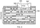
- Fig. 3 shows a cross-section of an IC according to the present invention.
- the uppermost interconnect layer 140 comprises a plurality of air-filled trenches 345 in the region under the bond pad 160, such that a number of pillars 340 of the dielectric material are formed.
- the pillars 340 ensure that the interconnect layer 140 can absorb mechanical forces exerted on the bond pad 160, e.g. during wire-bonding the bond pad 160 to a wire (not shown), because the pillars 340 have the ability to deform under the mechanical forces.
- the introduction of the pillars 340 is not limited to the uppermost interconnect layer 140 but may be extended to any interconnect layer that has to absorb such mechanical forces. For this reason, a further air-filled trench 325 is shown in the interconnect layer immediately below the uppermost interconnect layer 140 in Fig. 3 .
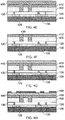
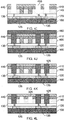
- FIG. 4a-m An embodiment of the method of the present invention facilitating the formation of air gaps in a layer such as the uppermost interconnect layer 140 is given in Figs. 4a-m .
- a substrate 100 including a number of interconnect layers 120 and via layers 130 is provided.
- the substrate 100 typically comprises semiconductor devices such as diodes, transistors, ESD protection and so on.
- the interconnect layers typically comprise a number of metal portions 125 that are separated by air gaps and/or dielectric material, as is well-known in the art, and the via layers 130 typically comprise a number of vias 135 interconnecting metal portions 125 in different interconnect layers 120. It is reiterated that such a stack may be formed in any suitable way.
- a dielectric layer 400 is deposited over the substrate stack, which will serve to form an interconnect layer 140 in accordance with the present invention.
- the dielectric material e.g. a high density low-k material or silicon oxide (SiO 2 ) may be deposited in any suitable way, e.g. by means of a vapor deposition technique or spin-on coating. Alternative techniques will be apparent to the skilled person. It is pointed out that in Fig 4a the layer thickness of dielectric material 400 is exaggerated for the purpose of clearly demonstrating the method of the present invention.
- the thickness of the dielectric material layer may be any suitable thickness and may for instance be similar to the thickness of lower interconnect layers 120.
- a hard mask 410 is deposited over the dielectric layer 400. It will be appreciated that this step is optional, because if a material such as SiO2 is used for the dielectric layer 400, the material itself may act as a hard mask. In case a low-k material is used for the dielectric layer 400, a hard mask 410 such as a SiO 2 mask may be formed over the dielectric layer 400. Any suitable deposition method may be applied.
- a resist layer 420 is applied to the hard mask 410, and subsequently patterned, as shown in Fig. 4c .
- Any suitable resist material may be used, such as a negative or positive photoresist, e.g. DNQ or Novolac.
- the photoresist may be applied in any suitable way, e.g. spin-coating.
- trenches 425 are etched in the hard mask 410 (if present) and the dielectric layer 400. This is shown in Fig. 4d .
- the trenches 425 are formed in a region of the dielectric material over which a bond pad will be formed in a subsequent processing step. Such an etch step is routine practice for the skilled practitioner and will not be explained in further detail for reasons of brevity only.
- the number of trenches 425 is not critical, as long as one or more pillars 340 of the dielectric material 400 are formed to ensure that the interconnect layer 140 will have sufficient flexibility to withstand mechanical forces associated with subsequent processing steps, as previously explained.
- the resist 420 may be removed after the trench formation.
- the trenches 425 are filled with a thermally decomposable polymer (TDP), which may be applied in any suitable way, e.g. spin-coating.
- TDP thermally decomposable polymer
- a TDP is a polymer that decomposes in the gaseous compounds when exposed to a high enough temperature. The exact temperature depends on the type of TDP used. Any suitable TDP may be used. Non-limiting examples include polynorbornene-based polymers, polyacrylate-based polymers and XP0733 marketed by Rohm HaasTM.
- excess TDP is removed, for instance by means of a chemical mechanical planarization (CMP) step, such that the hard mask 410 if present or the dielectric material 400 is exposed.
- CMP chemical mechanical planarization
- this further hard mask 440 must be a porous material because the decomposition products of the TDP in the trenches 425 must be able to escape the trenches 425 through this hard mask 440.
- Suitable materials for the hard mask 440 include SiOCH based materials, amongst others.
- the further hard mask 440 may be deposited using any suitable deposition technique, as already explained for the hard mask 410. Preferably, when using SiOCH-based materials, the further hard mask 440 is deposited by means of plasmaenhanced chemical vapor deposition (PE-CVD).
- a further resist 450 is deposited over the further hard mask 440 and subsequently patterned.
- the further resist may be the same resist material as used for resist 420, or may be a different resist material.
- further trenches 455 are etched through the hard masks 410 and 440 and the dielectric material 400 using any suitable etching technique. Following the etching step, the further resist 450 may be removed, thereby exposing the further hard mask 440.
- the further trenches 455 are subsequently filled with a metal to form metal tracks through the dielectric material 400.
- the metal is copper, which may be deposited in any suitable way, e.g. by means of a Damascene process, which is completed by the removal of the excess copper over the further trenches 455, e.g. by means of CMP, such that the further hard mask 440 is exposed again. This is shown in Fig. 4k .
- the interconnect layer 140 of the present invention can now be formed by decomposing the TDP in the trenches 425. To this end, the substrate stack is exposed to a thermal budget that is sufficient to decompose the TDP, causing the decomposition products to escape the trenches 425 through the porous further hard mask 440. Upon completion of the TDP decomposition, an interconnect layer 140 comprising metal portions 125 and air-filled trenches 325 is formed, as shown in Fig. 4l .
- Fig. 4m The manufacture of the IC of the present invention may now be completed, as shown in Fig. 4m .
- this includes the formation of a bond pad 160 over the portion of the interconnect layer 140 comprising the air-filled trenched 325.
- Other further processing steps which may or may not include the formation of a final via layer 130 over the interconnect layer 140, the formation of the planarization layer 150 and the formation of a metal cap 170 on the bond pad 160 are not essential to the present invention and may be implemented in any suitable way.
Landscapes
- Internal Circuitry In Semiconductor Integrated Circuit Devices (AREA)
Description
- The present invention relates to a method of manufacturing an integrated circuit (IC) comprising providing a substrate stack carrying a first layer comprising conductive regions and forming a interconnect layer over the first layer, said interconnect layer comprising a portion to be oriented between a bond pad and the substrate stack.
- The present invention further relates to an IC comprising a bond pad; a substrate stack carrying a first layer comprising conductive regions; and a layer of a dielectric material over the first layer, said dielectric material comprising a portion between the bond pad and the substrate stack.
- In deep submicron IC technology, one of the main design challenges is the provision of metal interconnects that, although being located in close vicinity to neighboring metal interconnects, experience little detrimental influence, e.g. capacitive coupling, from their neighbors. Several solutions have been proposed. For instance, low-k materials have been introduced in the buried interconnect layers between the metal tracks of such layers to reduce the amount of capacitive coupling. Recently, proposals even include the replacement of the low-k material in such buried interconnect layers with air gaps to further reduce the capacitive coupling between neighboring interconnects. An example of the introduction of air gaps is for instance disclosed in "Advanced Cu interconnects using air gaps" by L.G. Gosset et al. in Microelectronic Engineering, 82 (2005), pages 321-332 arid in "The evolution of multi-level air gap integration towards 32 nm node interconnects" by R. Daamen et al. in Microelectronic Engineering, 84 (2007), pages 2177-2183.
- However, such measures are not appropriate for the uppermost interconnect layer because this layer is typically exposed to significant mechanical forces during the back-end processing steps in the IC manufacturing. This is for instance demonstrated in
Fig. 1 , which shows a cross-section of an integrated circuit. Thesubstrate 100, which typically includes the semiconductor devices such as transistors, diodes and so on, is covered by a number ofinterconnect layers 120, each comprising patternedmetal portions 125 separated by a suitable dielectric material. Theinterconnect layers 120 are typically separated by vialayers 130, includingvias 135 that interconnectmetal portions 125 indifferent interconnect layers 120. Theuppermost interconnect layer 140 is the interconnect layer that is closest to thebond pads 160 of the IC, which are typically embedded in apassivation layer 150. InFig. 1 , theuppermost interconnect layer 140 has adielectric material portion 145 located underneath thebond pad 160. InFig. 1 , thebond pad 160 is shown with ametal cap 170. - Upon wire-bonding the
bond pad 160, the mechanical forces on thebond pad 160 to ensure a good connection between thebond pad 160 and a wire (not shown) can cause damage to thedielectric material portion 145, e.g. delamination, cracking or even collapse of theinterconnect layer 140. Similar mechanical forces may for instance be experienced during some packaging steps, e.g. molding. Such damage is likely to cause electrical failures within the IC at some point during its lifetime. For this reason, relatively brittle low-k materials are avoided in the uppermost interconnect layers of an IC. However, even more robust dielectric materials, e.g. SiO2, can still suffer damage when exposed to such mechanical forces. - A known solution is disclosed in
Fig. 2 , which shows a cross-section of another IC design. Here, thearea 245 of theinterconnect layer 140 under thebond pad 160 is filled with metal interconnect portions to ensure that the metal, which typically is more rigid than the dielectric material in theinterconnect layer 140 in between the metal portions, absorbs most of the pressure forces exerted on the IC during subsequent process steps. However, the introduction of such a design rule significantly reduces the flexibility of the interconnect design, which may prohibit the adequate routing of the required interconnections in the design stage of the IC. -
US 2004/0245637 describes a method for forming interlevel dielectric levels in a multilevel interconnect structure formed by a damsine process. -
US2004/222533 describes a semiconductor device which includes a foundation having a first conductive region, and an interconnection layer provided separate from the foundation. A first region occupying a range from the foundation to the interconnection layer is filled with gas or provided with a first interlayer dielectric film. - The invention is defined in the accompanying claims.
- An embodiment of the invention can provide a method of manufacturing an IC having improved structural integrity.
- An embodiment of the invention can provide an IC having improved structural integrity.
- A method of manufacturing an integrated circuit comprising:
- providing a stack of layers on a substrate, the stack including at least a first layer (130), the first layer comprising conductive regions (135);
- forming an interconnect layer (140) over the first layer, said interconnect layer comprising a dielectric material portion (400) to be provided between a bond pad (150) and the substrate stack;
- forming a plurality of trenches (425) in said dielectric material portion;
- filling said trenches with a thermally degradable polymer (430);
- forming a porous capping layer (440) over the interconnect layer (140);
- thermally decomposing said polymer; and
- forming the bond pad (160) over said dielectric material portion.
- In accordance with an embodiment of the invention, a portion of a dielectric material in an interconnect layer underneath a bond pad is patterned such that a plurality of air gaps are formed, thereby defining one or more pillars of the dielectric material underneath the bond pad area. The pillars provide structural support for preventing damage to the interconnect layer under pressure exerted on the bond pad. The first layer may be a metal layer, which may be patterned.
- The formation of pillars of the dielectric material under the bond pad improves the elastical flexibility of the portion of the interconnect layer under the bond pad compared to a continuous dielectric material portion as shown in
Fig. 1 . So even though less dielectric material may be present under the bond pad, the resilience of the interconnect layer is nevertheless improved. The dielectric material may be chosen to be any material that has a high enough density to withstand the mechanical forces exerted e.g. during the wire-bonding process, e.g. silicon oxide or a dense low-k material. - The introduction of the air-filled trenches has the additional advantage that the dielectric constant of the dielectric material has become less critical because the air-filled trenches help to reduce the capacitive coupling between neighboring metal tracks. This enables the choice of dielectric materials for the uppermost interconnect layer that would not have been considered previously because of the performance issues associated with the capacitive coupling between neighboring metal portions in this interconnect layer.
- The dielectric material may be used in combination with a fluorosilicate glass for the via layers, which further improves the structural integrity of the IC.
- The trenches may be formed by forming a hard mask over the interconnect layer; depositing a resist over the hard mask; patterning the resist; and etching the plurality of trenches. The resist may be removed after said etching step. Any suitable hard mask and resist material may be used.
- The trenches may be filled by depositing the thermally degradable polymer over the interconnect layer, thereby filling said trenches; and subsequently removing excess thermally degradable polymer. Any suitable deposition technique such as spin-coating may be used.
- In an embodiment, the method further comprises forming, in said portion, at least one further trench over at least one of said regions following said filling step, and wherein forming the further layer comprising forming a further metal layer over the interconnect layer, said forming step including filling the at least one further trench with the further metal. In this case, the portion underneath the bond pad comprises both air-filled trenches and metal-filled, e.g. copper-filled trenches, with the air-filled trenches typically located between a pair of metal-filled trenches, with at least one of said metal-filled trenches being located in said portion.
- The at least one further trench may be formed by depositing a further hard mask over the interconnect layer; depositing a further resist over the further hard mask; patterning the further resist; and etching the at least one further trench. The further resist may be removed after forming the further trench in order to facilitate deposition of the filler material over the interconnect layer.
- According to a further aspect of the present invention, there is provided An integrated circuit comprising:
- a bond pad (160);
- a stack of layers on a substrate, the stack including at least a first layer (130), wherein the first layer comprises conductive regions (135); and
- an interconnect layer (140) over the first layer (130), the interconnect layer comprising a dielectric material portion (400) between the bond pad (160) and the substrate stack, said dielectric material portion comprising a plurality of air-filled trenches (325) defining at least one pillar (340) of the
- Such an IC benefits from improved structural integrity under its bond pads, as previously explained. Such an IC may be integrated in an electronic device, which can benefit from improved reliability of its functionality controlled by the IC of the present invention.
- Embodiments of the invention are described in more detail and by way of non-limiting examples with reference to the accompanying drawings, wherein:
-
Fig. 1 depicts a typical bond pad design on a substrate stack; -
Fig. 2 depicts another typical bond pad design on a substrate stack; -
Fig. 3 depicts a bond pad design in accordance with an embodiment of the present invention; and -
Figs. 4a-m depict the various steps of a method in accordance with an embodiment of the present invention. - It should be understood that the Figures are merely schematic and are not drawn to scale. It should also be understood that the same reference numerals are used throughout the Figures to indicate the same or similar parts.
-
Fig. 3 shows a cross-section of an IC according to the present invention. Compared toFig. 1 , theuppermost interconnect layer 140 comprises a plurality of air-filledtrenches 345 in the region under thebond pad 160, such that a number ofpillars 340 of the dielectric material are formed. Thepillars 340 ensure that theinterconnect layer 140 can absorb mechanical forces exerted on thebond pad 160, e.g. during wire-bonding thebond pad 160 to a wire (not shown), because thepillars 340 have the ability to deform under the mechanical forces. - It will be appreciated that the introduction of the
pillars 340 is not limited to theuppermost interconnect layer 140 but may be extended to any interconnect layer that has to absorb such mechanical forces. For this reason, a further air-filledtrench 325 is shown in the interconnect layer immediately below theuppermost interconnect layer 140 inFig. 3 . - It will also be appreciated that the materials and process steps chosen for realizing the various components of the IC of the present invention other than the formation of the air-filled trenches are not critically important to the present invention. Any suitable material and/or process steps may be used.
- An embodiment of the method of the present invention facilitating the formation of air gaps in a layer such as the
uppermost interconnect layer 140 is given inFigs. 4a-m . - As shown in
Fig. 4a , asubstrate 100 including a number ofinterconnect layers 120 and vialayers 130 is provided. Thesubstrate 100 typically comprises semiconductor devices such as diodes, transistors, ESD protection and so on. The interconnect layers typically comprise a number ofmetal portions 125 that are separated by air gaps and/or dielectric material, as is well-known in the art, and the via layers 130 typically comprise a number ofvias 135 interconnectingmetal portions 125 in different interconnect layers 120. It is reiterated that such a stack may be formed in any suitable way. - In accordance with the present invention, a
dielectric layer 400 is deposited over the substrate stack, which will serve to form aninterconnect layer 140 in accordance with the present invention. The dielectric material, e.g. a high density low-k material or silicon oxide (SiO2) may be deposited in any suitable way, e.g. by means of a vapor deposition technique or spin-on coating. Alternative techniques will be apparent to the skilled person. It is pointed out that inFig 4a the layer thickness ofdielectric material 400 is exaggerated for the purpose of clearly demonstrating the method of the present invention. The thickness of the dielectric material layer may be any suitable thickness and may for instance be similar to the thickness of lower interconnect layers 120. - In a next step shown in
Fig. 4b , ahard mask 410 is deposited over thedielectric layer 400. It will be appreciated that this step is optional, because if a material such as SiO2 is used for thedielectric layer 400, the material itself may act as a hard mask. In case a low-k material is used for thedielectric layer 400, ahard mask 410 such as a SiO2 mask may be formed over thedielectric layer 400. Any suitable deposition method may be applied. - A resist
layer 420 is applied to thehard mask 410, and subsequently patterned, as shown inFig. 4c . Any suitable resist material may be used, such as a negative or positive photoresist, e.g. DNQ or Novolac. The photoresist may be applied in any suitable way, e.g. spin-coating. - Next,
trenches 425 are etched in the hard mask 410 (if present) and thedielectric layer 400. This is shown inFig. 4d . Thetrenches 425 are formed in a region of the dielectric material over which a bond pad will be formed in a subsequent processing step. Such an etch step is routine practice for the skilled practitioner and will not be explained in further detail for reasons of brevity only. The number oftrenches 425 is not critical, as long as one ormore pillars 340 of thedielectric material 400 are formed to ensure that theinterconnect layer 140 will have sufficient flexibility to withstand mechanical forces associated with subsequent processing steps, as previously explained. The resist 420 may be removed after the trench formation. - As shown in
Fig. 4e , thetrenches 425 are filled with a thermally decomposable polymer (TDP), which may be applied in any suitable way, e.g. spin-coating. A TDP is a polymer that decomposes in the gaseous compounds when exposed to a high enough temperature. The exact temperature depends on the type of TDP used. Any suitable TDP may be used. Non-limiting examples include polynorbornene-based polymers, polyacrylate-based polymers and XP0733 marketed by Rohm Haas™. As shown inFig. 4f , excess TDP is removed, for instance by means of a chemical mechanical planarization (CMP) step, such that thehard mask 410 if present or thedielectric material 400 is exposed. - Next, another
hard mask 440 is formed over the exposedhard mask 410 or thedielectric material 400. This is shown inFig. 4g . This furtherhard mask 440 must be a porous material because the decomposition products of the TDP in thetrenches 425 must be able to escape thetrenches 425 through thishard mask 440. Suitable materials for thehard mask 440 include SiOCH based materials, amongst others. The furtherhard mask 440 may be deposited using any suitable deposition technique, as already explained for thehard mask 410. Preferably, when using SiOCH-based materials, the furtherhard mask 440 is deposited by means of plasmaenhanced chemical vapor deposition (PE-CVD). - In the step shown in
Fig. 4h , a further resist 450 is deposited over the furtherhard mask 440 and subsequently patterned. The further resist may be the same resist material as used for resist 420, or may be a different resist material. In a subsequent step, as shown inFig. 4i ,further trenches 455 are etched through thehard masks dielectric material 400 using any suitable etching technique. Following the etching step, the further resist 450 may be removed, thereby exposing the furtherhard mask 440. - The
further trenches 455 are subsequently filled with a metal to form metal tracks through thedielectric material 400. In a preferred embodiment, the metal is copper, which may be deposited in any suitable way, e.g. by means of a Damascene process, which is completed by the removal of the excess copper over thefurther trenches 455, e.g. by means of CMP, such that the furtherhard mask 440 is exposed again. This is shown inFig. 4k . - The
interconnect layer 140 of the present invention can now be formed by decomposing the TDP in thetrenches 425. To this end, the substrate stack is exposed to a thermal budget that is sufficient to decompose the TDP, causing the decomposition products to escape thetrenches 425 through the porous furtherhard mask 440. Upon completion of the TDP decomposition, aninterconnect layer 140 comprisingmetal portions 125 and air-filledtrenches 325 is formed, as shown inFig. 4l . - The manufacture of the IC of the present invention may now be completed, as shown in
Fig. 4m . In accordance with the present invention, this includes the formation of abond pad 160 over the portion of theinterconnect layer 140 comprising the air-filledtrenched 325. Other further processing steps, which may or may not include the formation of a final vialayer 130 over theinterconnect layer 140, the formation of theplanarization layer 150 and the formation of ametal cap 170 on thebond pad 160 are not essential to the present invention and may be implemented in any suitable way. - It should be noted that the above-mentioned embodiments illustrate rather than limit the invention, and that those skilled in the art will be able to design many alternative embodiments without departing from the scope of the appended claims. In the claims, any reference signs placed between parentheses shall not be construed as limiting the claim. The word "comprising" does not exclude the presence of elements or steps other than those listed in a claim. The word "a" or "an" preceding an element does not exclude the presence of a plurality of such elements. The mere fact that certain measures are recited in mutually different dependent claims does not indicate that a combination of these measures cannot be used to advantage.
Claims (11)
- A method of manufacturing an integrated circuit comprising:providing a stack of layers on a substrate, the stack including at least a first layer (130), the first layer comprising conductive regions (135);forming an interconnect layer (140) over the first layer, said interconnect layer comprising a dielectric material portion (400) to be provide between a bond pad (150) and the stack of layers;forming a plurality of trenches (425) in said dielectric material portion;filling said trenches with a thermally degradable polymer (430);forming a porous capping layer (440) over the interconnect layer (140);thermally decomposing said polymer; andforming the bond pad (160) over said dielectric material portion.
- A method according to claim 1, said trench forming step comprising:forming a hard mask (410) over the interconnect layer (140);depositing a resist (420) over the hard mask (410);patterning the resist (420); andetching the plurality of trenches (425).
- A method according to claim 1 or 2, said filling step comprising:depositing the thermally degradable polymer (430) over the interconnect layer (140), thereby filling said trenches; andremoving excess thermally degradable polymer (430).
- A method according to any of claims 1-3, further comprising:forming at least one further trench (455) over at least one of said conductive regions (135), wherein the at least one further trench is provided in the dielectric material portion following the step of forming the porous capping layer; andforming a metal layer (460) over the interconnect layer (140), said forming step including filling the at least one further trench (455) with the metal.
- A method according to claim 4, said further trench formation comprising:depositing a further resist (450) over the porous capping layer (440);patterning the further resist (450); andetching the at least one further trench (455).
- A method according to any of claims 1-5, wherein the first layer (130) is a via layer comprising a plurality of vias (135).
- An integrated circuit comprising:a bond pad (160);a stack of layers on a substrate, the stack including at least a first layer (130), wherein the first layer comprises conductive regions (135); andan interconnect layer (140) over the first layer (130), the interconnect layer comprising a dielectric material portion (400) between the bond pad (160) and the stack of layers, said dielectric-material portion comprising a plurality of air-filled trenches (325) defining at least one pillar (340) of the dielectric material (400), said air-filled trenches (325) being capped by a porous capping layer (440).
- An integrated circuit according to claim 7, said interconnect layer (140) further comprising a metal-filled trench (125) in conductive contact with one of said conductive regions (135).
- An integrated circuit according to claim 8, wherein the dielectric material portion comprises the metal-filled trench (125).
- An integrated circuit according to claim 8 or 9, wherein the metal-filled trench (125) is filled with copper.
- An electronic device comprising an integrated circuit according to any of claims 8-10.
Priority Applications (1)
| Application Number | Priority Date | Filing Date | Title |
|---|---|---|---|
| EP09754245.0A EP2283517B1 (en) | 2008-05-27 | 2009-05-19 | Integrated circuit manufacturing method and integrated circuit |
Applications Claiming Priority (3)
| Application Number | Priority Date | Filing Date | Title |
|---|---|---|---|
| EP08156980 | 2008-05-27 | ||
| PCT/IB2009/052084 WO2009144618A1 (en) | 2008-05-27 | 2009-05-19 | Integrated circuit manufacturing method and integrated circuit |
| EP09754245.0A EP2283517B1 (en) | 2008-05-27 | 2009-05-19 | Integrated circuit manufacturing method and integrated circuit |
Publications (2)
| Publication Number | Publication Date |
|---|---|
| EP2283517A1 EP2283517A1 (en) | 2011-02-16 |
| EP2283517B1 true EP2283517B1 (en) | 2016-07-13 |
Family
ID=40996530
Family Applications (1)
| Application Number | Title | Priority Date | Filing Date |
|---|---|---|---|
| EP09754245.0A Not-in-force EP2283517B1 (en) | 2008-05-27 | 2009-05-19 | Integrated circuit manufacturing method and integrated circuit |
Country Status (3)
| Country | Link |
|---|---|
| US (1) | US8722527B2 (en) |
| EP (1) | EP2283517B1 (en) |
| WO (1) | WO2009144618A1 (en) |
Families Citing this family (3)
| Publication number | Priority date | Publication date | Assignee | Title |
|---|---|---|---|---|
| US10896888B2 (en) * | 2018-03-15 | 2021-01-19 | Microchip Technology Incorporated | Integrated circuit (IC) device including a force mitigation system for reducing under-pad damage caused by wire bond |
| US11309266B2 (en) * | 2020-05-28 | 2022-04-19 | Nanya Technology Corporation | Semiconductor device structure with air gap and method for forming the same |
| US12628642B2 (en) * | 2023-03-06 | 2026-05-12 | Nanya Technology Corporation | Circuit structure including at least one air gap and method for manufacturing the same |
Family Cites Families (6)
| Publication number | Priority date | Publication date | Assignee | Title |
|---|---|---|---|---|
| US6815329B2 (en) | 2000-02-08 | 2004-11-09 | International Business Machines Corporation | Multilayer interconnect structure containing air gaps and method for making |
| US6867125B2 (en) | 2002-09-26 | 2005-03-15 | Intel Corporation | Creating air gap in multi-level metal interconnects using electron beam to remove sacrificial material |
| US6930034B2 (en) | 2002-12-27 | 2005-08-16 | International Business Machines Corporation | Robust ultra-low k interconnect structures using bridge-then-metallization fabrication sequence |
| JP4102246B2 (en) | 2003-04-28 | 2008-06-18 | 株式会社東芝 | Semiconductor device and manufacturing method thereof |
| US6713835B1 (en) | 2003-05-22 | 2004-03-30 | International Business Machines Corporation | Method for manufacturing a multi-level interconnect structure |
| US6890828B2 (en) | 2003-06-05 | 2005-05-10 | International Business Machines Corporation | Method for supporting a bond pad in a multilevel interconnect structure and support structure formed thereby |
-
2009
- 2009-05-19 US US12/994,628 patent/US8722527B2/en not_active Expired - Fee Related
- 2009-05-19 EP EP09754245.0A patent/EP2283517B1/en not_active Not-in-force
- 2009-05-19 WO PCT/IB2009/052084 patent/WO2009144618A1/en not_active Ceased
Also Published As
| Publication number | Publication date |
|---|---|
| WO2009144618A1 (en) | 2009-12-03 |
| EP2283517A1 (en) | 2011-02-16 |
| US8722527B2 (en) | 2014-05-13 |
| US20120126408A1 (en) | 2012-05-24 |
Similar Documents
| Publication | Publication Date | Title |
|---|---|---|
| CN100382314C (en) | semiconductor chip | |
| US7285474B2 (en) | Air-gap insulated interconnections | |
| KR101580941B1 (en) | Structure and method for strain-relieved tsv | |
| US7094689B2 (en) | Air gap interconnect structure and method thereof | |
| EP2777071B1 (en) | Protection spacer for protecting low-k wiring layers during patterning of through substrate vias | |
| US7250681B2 (en) | Semiconductor device and a method of manufacturing the semiconductor device | |
| CN107665857B (en) | Multiple Patterning for Forming Vias with Straight Profiles | |
| CN101459055B (en) | Manufacturing method of semiconductor device | |
| KR101735912B1 (en) | Semiconductor device having air gap structures and method of fabricating thereof | |
| US6858936B2 (en) | Semiconductor device having an improved construction in the interlayer insulating film | |
| JP4102246B2 (en) | Semiconductor device and manufacturing method thereof | |
| US9595465B2 (en) | Vias and methods of formation thereof | |
| US8455985B2 (en) | Integrated circuit devices having selectively strengthened composite interlayer insulation layers and methods of fabricating the same | |
| JP2008166726A (en) | Semiconductor device and manufacturing method thereof | |
| US20100330799A1 (en) | Semiconductor device and process for producing the same | |
| US20100323477A1 (en) | Interconnections of an integrated electronic circuit | |
| CN100541760C (en) | Lateral Distribution Control of Air Gaps in Interconnects | |
| KR100726917B1 (en) | Semiconductor device and its manufacturing method | |
| US7319271B2 (en) | Semiconductor device | |
| US8722527B2 (en) | Integrated circuit manufacturing method and integrated circuit | |
| JP2012134422A (en) | Semiconductor device and manufacturing method of the same | |
| US7763521B2 (en) | Metal wiring and method for forming the same | |
| US20160372375A1 (en) | Superimposed transistors with auto-aligned active zone of the upper transistor | |
| JP2006351732A (en) | Process for fabricating semiconductor device | |
| JP2007073808A (en) | Semiconductor device manufacturing method and semiconductor device |
Legal Events
| Date | Code | Title | Description |
|---|---|---|---|
| PUAI | Public reference made under article 153(3) epc to a published international application that has entered the european phase |
Free format text: ORIGINAL CODE: 0009012 |
|
| 17P | Request for examination filed |
Effective date: 20101227 |
|
| AK | Designated contracting states |
Kind code of ref document: A1 Designated state(s): AT BE BG CH CY CZ DE DK EE ES FI FR GB GR HR HU IE IS IT LI LT LU LV MC MK MT NL NO PL PT RO SE SI SK TR |
|
| AX | Request for extension of the european patent |
Extension state: AL BA RS |
|
| DAX | Request for extension of the european patent (deleted) | ||
| 17Q | First examination report despatched |
Effective date: 20150415 |
|
| GRAP | Despatch of communication of intention to grant a patent |
Free format text: ORIGINAL CODE: EPIDOSNIGR1 |
|
| RIC1 | Information provided on ipc code assigned before grant |
Ipc: H01L 21/768 20060101AFI20150819BHEP Ipc: H01L 23/00 20060101ALI20150819BHEP |
|
| INTG | Intention to grant announced |
Effective date: 20150902 |
|
| GRAS | Grant fee paid |
Free format text: ORIGINAL CODE: EPIDOSNIGR3 |
|
| GRAP | Despatch of communication of intention to grant a patent |
Free format text: ORIGINAL CODE: EPIDOSNIGR1 |
|
| GRAS | Grant fee paid |
Free format text: ORIGINAL CODE: EPIDOSNIGR3 |
|
| INTG | Intention to grant announced |
Effective date: 20160414 |
|
| GRAA | (expected) grant |
Free format text: ORIGINAL CODE: 0009210 |
|
| AK | Designated contracting states |
Kind code of ref document: B1 Designated state(s): AT BE BG CH CY CZ DE DK EE ES FI FR GB GR HR HU IE IS IT LI LT LU LV MC MK MT NL NO PL PT RO SE SI SK TR |
|
| REG | Reference to a national code |
Ref country code: GB Ref legal event code: FG4D |
|
| REG | Reference to a national code |
Ref country code: AT Ref legal event code: REF Ref document number: 812926 Country of ref document: AT Kind code of ref document: T Effective date: 20160715 Ref country code: CH Ref legal event code: EP |
|
| REG | Reference to a national code |
Ref country code: IE Ref legal event code: FG4D |
|
| REG | Reference to a national code |
Ref country code: DE Ref legal event code: R096 Ref document number: 602009039719 Country of ref document: DE |
|
| REG | Reference to a national code |
Ref country code: LT Ref legal event code: MG4D |
|
| REG | Reference to a national code |
Ref country code: NL Ref legal event code: MP Effective date: 20160713 |
|
| REG | Reference to a national code |
Ref country code: AT Ref legal event code: MK05 Ref document number: 812926 Country of ref document: AT Kind code of ref document: T Effective date: 20160713 |
|
| PG25 | Lapsed in a contracting state [announced via postgrant information from national office to epo] |
Ref country code: LT Free format text: LAPSE BECAUSE OF FAILURE TO SUBMIT A TRANSLATION OF THE DESCRIPTION OR TO PAY THE FEE WITHIN THE PRESCRIBED TIME-LIMIT Effective date: 20160713 Ref country code: NO Free format text: LAPSE BECAUSE OF FAILURE TO SUBMIT A TRANSLATION OF THE DESCRIPTION OR TO PAY THE FEE WITHIN THE PRESCRIBED TIME-LIMIT Effective date: 20161013 Ref country code: NL Free format text: LAPSE BECAUSE OF FAILURE TO SUBMIT A TRANSLATION OF THE DESCRIPTION OR TO PAY THE FEE WITHIN THE PRESCRIBED TIME-LIMIT Effective date: 20160713 Ref country code: IS Free format text: LAPSE BECAUSE OF FAILURE TO SUBMIT A TRANSLATION OF THE DESCRIPTION OR TO PAY THE FEE WITHIN THE PRESCRIBED TIME-LIMIT Effective date: 20161113 Ref country code: IT Free format text: LAPSE BECAUSE OF FAILURE TO SUBMIT A TRANSLATION OF THE DESCRIPTION OR TO PAY THE FEE WITHIN THE PRESCRIBED TIME-LIMIT Effective date: 20160713 Ref country code: HR Free format text: LAPSE BECAUSE OF FAILURE TO SUBMIT A TRANSLATION OF THE DESCRIPTION OR TO PAY THE FEE WITHIN THE PRESCRIBED TIME-LIMIT Effective date: 20160713 Ref country code: FI Free format text: LAPSE BECAUSE OF FAILURE TO SUBMIT A TRANSLATION OF THE DESCRIPTION OR TO PAY THE FEE WITHIN THE PRESCRIBED TIME-LIMIT Effective date: 20160713 |
|
| PG25 | Lapsed in a contracting state [announced via postgrant information from national office to epo] |
Ref country code: LV Free format text: LAPSE BECAUSE OF FAILURE TO SUBMIT A TRANSLATION OF THE DESCRIPTION OR TO PAY THE FEE WITHIN THE PRESCRIBED TIME-LIMIT Effective date: 20160713 Ref country code: PL Free format text: LAPSE BECAUSE OF FAILURE TO SUBMIT A TRANSLATION OF THE DESCRIPTION OR TO PAY THE FEE WITHIN THE PRESCRIBED TIME-LIMIT Effective date: 20160713 Ref country code: ES Free format text: LAPSE BECAUSE OF FAILURE TO SUBMIT A TRANSLATION OF THE DESCRIPTION OR TO PAY THE FEE WITHIN THE PRESCRIBED TIME-LIMIT Effective date: 20160713 Ref country code: GR Free format text: LAPSE BECAUSE OF FAILURE TO SUBMIT A TRANSLATION OF THE DESCRIPTION OR TO PAY THE FEE WITHIN THE PRESCRIBED TIME-LIMIT Effective date: 20161014 Ref country code: AT Free format text: LAPSE BECAUSE OF FAILURE TO SUBMIT A TRANSLATION OF THE DESCRIPTION OR TO PAY THE FEE WITHIN THE PRESCRIBED TIME-LIMIT Effective date: 20160713 Ref country code: BE Free format text: LAPSE BECAUSE OF FAILURE TO SUBMIT A TRANSLATION OF THE DESCRIPTION OR TO PAY THE FEE WITHIN THE PRESCRIBED TIME-LIMIT Effective date: 20160713 Ref country code: SE Free format text: LAPSE BECAUSE OF FAILURE TO SUBMIT A TRANSLATION OF THE DESCRIPTION OR TO PAY THE FEE WITHIN THE PRESCRIBED TIME-LIMIT Effective date: 20160713 Ref country code: PT Free format text: LAPSE BECAUSE OF FAILURE TO SUBMIT A TRANSLATION OF THE DESCRIPTION OR TO PAY THE FEE WITHIN THE PRESCRIBED TIME-LIMIT Effective date: 20161114 |
|
| REG | Reference to a national code |
Ref country code: DE Ref legal event code: R097 Ref document number: 602009039719 Country of ref document: DE |
|
| REG | Reference to a national code |
Ref country code: FR Ref legal event code: PLFP Year of fee payment: 9 |
|
| PG25 | Lapsed in a contracting state [announced via postgrant information from national office to epo] |
Ref country code: RO Free format text: LAPSE BECAUSE OF FAILURE TO SUBMIT A TRANSLATION OF THE DESCRIPTION OR TO PAY THE FEE WITHIN THE PRESCRIBED TIME-LIMIT Effective date: 20160713 Ref country code: EE Free format text: LAPSE BECAUSE OF FAILURE TO SUBMIT A TRANSLATION OF THE DESCRIPTION OR TO PAY THE FEE WITHIN THE PRESCRIBED TIME-LIMIT Effective date: 20160713 |
|
| PLBE | No opposition filed within time limit |
Free format text: ORIGINAL CODE: 0009261 |
|
| STAA | Information on the status of an ep patent application or granted ep patent |
Free format text: STATUS: NO OPPOSITION FILED WITHIN TIME LIMIT |
|
| PG25 | Lapsed in a contracting state [announced via postgrant information from national office to epo] |
Ref country code: CZ Free format text: LAPSE BECAUSE OF FAILURE TO SUBMIT A TRANSLATION OF THE DESCRIPTION OR TO PAY THE FEE WITHIN THE PRESCRIBED TIME-LIMIT Effective date: 20160713 Ref country code: BG Free format text: LAPSE BECAUSE OF FAILURE TO SUBMIT A TRANSLATION OF THE DESCRIPTION OR TO PAY THE FEE WITHIN THE PRESCRIBED TIME-LIMIT Effective date: 20161013 Ref country code: SK Free format text: LAPSE BECAUSE OF FAILURE TO SUBMIT A TRANSLATION OF THE DESCRIPTION OR TO PAY THE FEE WITHIN THE PRESCRIBED TIME-LIMIT Effective date: 20160713 Ref country code: DK Free format text: LAPSE BECAUSE OF FAILURE TO SUBMIT A TRANSLATION OF THE DESCRIPTION OR TO PAY THE FEE WITHIN THE PRESCRIBED TIME-LIMIT Effective date: 20160713 |
|
| 26N | No opposition filed |
Effective date: 20170418 |
|
| PG25 | Lapsed in a contracting state [announced via postgrant information from national office to epo] |
Ref country code: SI Free format text: LAPSE BECAUSE OF FAILURE TO SUBMIT A TRANSLATION OF THE DESCRIPTION OR TO PAY THE FEE WITHIN THE PRESCRIBED TIME-LIMIT Effective date: 20160713 Ref country code: LU Free format text: LAPSE BECAUSE OF NON-PAYMENT OF DUE FEES Effective date: 20170531 |
|
| REG | Reference to a national code |
Ref country code: CH Ref legal event code: PL |
|
| PG25 | Lapsed in a contracting state [announced via postgrant information from national office to epo] |
Ref country code: MC Free format text: LAPSE BECAUSE OF FAILURE TO SUBMIT A TRANSLATION OF THE DESCRIPTION OR TO PAY THE FEE WITHIN THE PRESCRIBED TIME-LIMIT Effective date: 20160713 |
|
| REG | Reference to a national code |
Ref country code: IE Ref legal event code: MM4A |
|
| PG25 | Lapsed in a contracting state [announced via postgrant information from national office to epo] |
Ref country code: CH Free format text: LAPSE BECAUSE OF NON-PAYMENT OF DUE FEES Effective date: 20170531 Ref country code: LI Free format text: LAPSE BECAUSE OF NON-PAYMENT OF DUE FEES Effective date: 20170531 |
|
| PG25 | Lapsed in a contracting state [announced via postgrant information from national office to epo] |
Ref country code: LU Free format text: LAPSE BECAUSE OF NON-PAYMENT OF DUE FEES Effective date: 20170519 |
|
| REG | Reference to a national code |
Ref country code: FR Ref legal event code: PLFP Year of fee payment: 10 |
|
| PG25 | Lapsed in a contracting state [announced via postgrant information from national office to epo] |
Ref country code: IE Free format text: LAPSE BECAUSE OF NON-PAYMENT OF DUE FEES Effective date: 20170519 |
|
| PGFP | Annual fee paid to national office [announced via postgrant information from national office to epo] |
Ref country code: DE Payment date: 20180419 Year of fee payment: 10 |
|
| PGFP | Annual fee paid to national office [announced via postgrant information from national office to epo] |
Ref country code: FR Payment date: 20180423 Year of fee payment: 10 |
|
| PG25 | Lapsed in a contracting state [announced via postgrant information from national office to epo] |
Ref country code: MT Free format text: LAPSE BECAUSE OF NON-PAYMENT OF DUE FEES Effective date: 20170519 |
|
| PGFP | Annual fee paid to national office [announced via postgrant information from national office to epo] |
Ref country code: GB Payment date: 20180419 Year of fee payment: 10 |
|
| PG25 | Lapsed in a contracting state [announced via postgrant information from national office to epo] |
Ref country code: HU Free format text: LAPSE BECAUSE OF FAILURE TO SUBMIT A TRANSLATION OF THE DESCRIPTION OR TO PAY THE FEE WITHIN THE PRESCRIBED TIME-LIMIT; INVALID AB INITIO Effective date: 20090519 |
|
| PG25 | Lapsed in a contracting state [announced via postgrant information from national office to epo] |
Ref country code: CY Free format text: LAPSE BECAUSE OF NON-PAYMENT OF DUE FEES Effective date: 20160713 |
|
| PG25 | Lapsed in a contracting state [announced via postgrant information from national office to epo] |
Ref country code: MK Free format text: LAPSE BECAUSE OF FAILURE TO SUBMIT A TRANSLATION OF THE DESCRIPTION OR TO PAY THE FEE WITHIN THE PRESCRIBED TIME-LIMIT Effective date: 20160713 |
|
| REG | Reference to a national code |
Ref country code: DE Ref legal event code: R119 Ref document number: 602009039719 Country of ref document: DE |
|
| GBPC | Gb: european patent ceased through non-payment of renewal fee |
Effective date: 20190519 |
|
| PG25 | Lapsed in a contracting state [announced via postgrant information from national office to epo] |
Ref country code: TR Free format text: LAPSE BECAUSE OF FAILURE TO SUBMIT A TRANSLATION OF THE DESCRIPTION OR TO PAY THE FEE WITHIN THE PRESCRIBED TIME-LIMIT Effective date: 20160713 |
|
| PG25 | Lapsed in a contracting state [announced via postgrant information from national office to epo] |
Ref country code: DE Free format text: LAPSE BECAUSE OF NON-PAYMENT OF DUE FEES Effective date: 20191203 Ref country code: GB Free format text: LAPSE BECAUSE OF NON-PAYMENT OF DUE FEES Effective date: 20190519 |
|
| PG25 | Lapsed in a contracting state [announced via postgrant information from national office to epo] |
Ref country code: FR Free format text: LAPSE BECAUSE OF NON-PAYMENT OF DUE FEES Effective date: 20190531 |