EP2282348A2 - Silicon carbide semiconductor structures, devices, and methods for making the same - Google Patents
Silicon carbide semiconductor structures, devices, and methods for making the same Download PDFInfo
- Publication number
- EP2282348A2 EP2282348A2 EP10171439A EP10171439A EP2282348A2 EP 2282348 A2 EP2282348 A2 EP 2282348A2 EP 10171439 A EP10171439 A EP 10171439A EP 10171439 A EP10171439 A EP 10171439A EP 2282348 A2 EP2282348 A2 EP 2282348A2
- Authority
- EP
- European Patent Office
- Prior art keywords
- base
- layer
- silicon carbide
- conductivity type
- shielding
- Prior art date
- Legal status (The legal status is an assumption and is not a legal conclusion. Google has not performed a legal analysis and makes no representation as to the accuracy of the status listed.)
- Withdrawn
Links
- 239000004065 semiconductor Substances 0.000 title claims abstract description 42
- HBMJWWWQQXIZIP-UHFFFAOYSA-N silicon carbide Chemical compound [Si+]#[C-] HBMJWWWQQXIZIP-UHFFFAOYSA-N 0.000 title claims abstract description 24
- 238000000034 method Methods 0.000 title claims abstract description 11
- 229910010271 silicon carbide Inorganic materials 0.000 title claims description 23
- 239000010410 layer Substances 0.000 claims abstract description 88
- 239000002344 surface layer Substances 0.000 claims abstract description 38
- 239000002019 doping agent Substances 0.000 claims description 35
- 150000002500 ions Chemical class 0.000 claims description 23
- 238000002513 implantation Methods 0.000 claims description 5
- 238000004519 manufacturing process Methods 0.000 claims description 5
- IJGRMHOSHXDMSA-UHFFFAOYSA-N Atomic nitrogen Chemical compound N#N IJGRMHOSHXDMSA-UHFFFAOYSA-N 0.000 claims description 4
- 239000004020 conductor Substances 0.000 claims description 3
- ZOXJGFHDIHLPTG-UHFFFAOYSA-N Boron Chemical compound [B] ZOXJGFHDIHLPTG-UHFFFAOYSA-N 0.000 claims description 2
- XAGFODPZIPBFFR-UHFFFAOYSA-N aluminium Chemical compound [Al] XAGFODPZIPBFFR-UHFFFAOYSA-N 0.000 claims description 2
- 229910052782 aluminium Inorganic materials 0.000 claims description 2
- 229910052796 boron Inorganic materials 0.000 claims description 2
- BHEPBYXIRTUNPN-UHFFFAOYSA-N hydridophosphorus(.) (triplet) Chemical compound [PH] BHEPBYXIRTUNPN-UHFFFAOYSA-N 0.000 claims description 2
- 229910052757 nitrogen Inorganic materials 0.000 claims description 2
- 238000005468 ion implantation Methods 0.000 abstract description 7
- 230000001747 exhibiting effect Effects 0.000 abstract 1
- VYPSYNLAJGMNEJ-UHFFFAOYSA-N Silicium dioxide Chemical compound O=[Si]=O VYPSYNLAJGMNEJ-UHFFFAOYSA-N 0.000 description 4
- 230000037230 mobility Effects 0.000 description 4
- 239000000463 material Substances 0.000 description 3
- 229910052681 coesite Inorganic materials 0.000 description 2
- 230000000052 comparative effect Effects 0.000 description 2
- 229910052906 cristobalite Inorganic materials 0.000 description 2
- 238000012986 modification Methods 0.000 description 2
- 230000004048 modification Effects 0.000 description 2
- 230000000737 periodic effect Effects 0.000 description 2
- 229910021420 polycrystalline silicon Inorganic materials 0.000 description 2
- 229920005591 polysilicon Polymers 0.000 description 2
- 239000000377 silicon dioxide Substances 0.000 description 2
- 229910052682 stishovite Inorganic materials 0.000 description 2
- 229910052905 tridymite Inorganic materials 0.000 description 2
- ZOKXTWBITQBERF-UHFFFAOYSA-N Molybdenum Chemical compound [Mo] ZOKXTWBITQBERF-UHFFFAOYSA-N 0.000 description 1
- 230000015556 catabolic process Effects 0.000 description 1
- 239000011365 complex material Substances 0.000 description 1
- 230000008021 deposition Effects 0.000 description 1
- 229910003460 diamond Inorganic materials 0.000 description 1
- 239000010432 diamond Substances 0.000 description 1
- 239000003989 dielectric material Substances 0.000 description 1
- 239000007772 electrode material Substances 0.000 description 1
- 238000010893 electron trap Methods 0.000 description 1
- 238000005516 engineering process Methods 0.000 description 1
- 230000005669 field effect Effects 0.000 description 1
- 230000036039 immunity Effects 0.000 description 1
- 239000012212 insulator Substances 0.000 description 1
- 230000005527 interface trap Effects 0.000 description 1
- 238000005259 measurement Methods 0.000 description 1
- 239000003607 modifier Substances 0.000 description 1
- 229910052750 molybdenum Inorganic materials 0.000 description 1
- 239000011733 molybdenum Substances 0.000 description 1
- 238000005457 optimization Methods 0.000 description 1
- 238000002161 passivation Methods 0.000 description 1
- 230000035515 penetration Effects 0.000 description 1
- 239000002243 precursor Substances 0.000 description 1
- 238000011160 research Methods 0.000 description 1
- 238000012546 transfer Methods 0.000 description 1
Images


Classifications
-
- H—ELECTRICITY
- H10—SEMICONDUCTOR DEVICES; ELECTRIC SOLID-STATE DEVICES NOT OTHERWISE PROVIDED FOR
- H10D—INORGANIC ELECTRIC SEMICONDUCTOR DEVICES
- H10D30/00—Field-effect transistors [FET]
- H10D30/60—Insulated-gate field-effect transistors [IGFET]
- H10D30/63—Vertical IGFETs
- H10D30/635—Vertical IGFETs having no inversion channels, e.g. vertical accumulation channel FETs [ACCUFET] or normally-on vertical IGFETs
-
- H—ELECTRICITY
- H10—SEMICONDUCTOR DEVICES; ELECTRIC SOLID-STATE DEVICES NOT OTHERWISE PROVIDED FOR
- H10D—INORGANIC ELECTRIC SEMICONDUCTOR DEVICES
- H10D62/00—Semiconductor bodies, or regions thereof, of devices having potential barriers
- H10D62/10—Shapes, relative sizes or dispositions of the regions of the semiconductor bodies; Shapes of the semiconductor bodies
- H10D62/113—Isolations within a component, i.e. internal isolations
- H10D62/114—PN junction isolations
-
- H—ELECTRICITY
- H10—SEMICONDUCTOR DEVICES; ELECTRIC SOLID-STATE DEVICES NOT OTHERWISE PROVIDED FOR
- H10D—INORGANIC ELECTRIC SEMICONDUCTOR DEVICES
- H10D62/00—Semiconductor bodies, or regions thereof, of devices having potential barriers
- H10D62/10—Shapes, relative sizes or dispositions of the regions of the semiconductor bodies; Shapes of the semiconductor bodies
- H10D62/102—Constructional design considerations for preventing surface leakage or controlling electric field concentration
- H10D62/103—Constructional design considerations for preventing surface leakage or controlling electric field concentration for increasing or controlling the breakdown voltage of reverse-biased devices
- H10D62/105—Constructional design considerations for preventing surface leakage or controlling electric field concentration for increasing or controlling the breakdown voltage of reverse-biased devices by having particular doping profiles, shapes or arrangements of PN junctions; by having supplementary regions, e.g. junction termination extension [JTE]
- H10D62/106—Constructional design considerations for preventing surface leakage or controlling electric field concentration for increasing or controlling the breakdown voltage of reverse-biased devices by having particular doping profiles, shapes or arrangements of PN junctions; by having supplementary regions, e.g. junction termination extension [JTE] having supplementary regions doped oppositely to or in rectifying contact with regions of the semiconductor bodies, e.g. guard rings with PN or Schottky junctions
- H10D62/107—Buried supplementary regions, e.g. buried guard rings
-
- H—ELECTRICITY
- H10—SEMICONDUCTOR DEVICES; ELECTRIC SOLID-STATE DEVICES NOT OTHERWISE PROVIDED FOR
- H10D—INORGANIC ELECTRIC SEMICONDUCTOR DEVICES
- H10D62/00—Semiconductor bodies, or regions thereof, of devices having potential barriers
- H10D62/80—Semiconductor bodies, or regions thereof, of devices having potential barriers characterised by the materials
- H10D62/83—Semiconductor bodies, or regions thereof, of devices having potential barriers characterised by the materials being Group IV materials, e.g. B-doped Si or undoped Ge
- H10D62/832—Semiconductor bodies, or regions thereof, of devices having potential barriers characterised by the materials being Group IV materials, e.g. B-doped Si or undoped Ge being Group IV materials comprising two or more elements, e.g. SiGe
- H10D62/8325—Silicon carbide
Definitions
- the present disclosure relates to silicon carbide MOS semiconductor structures and devices, such as a field-effect transistors, and methods of making these.
- SiC inversion mode MOSFETs have very low channel mobilities caused by excessive electron trapping due to SiC/SiO 2 interface traps and surface scattering. Instead of achieving the expected value of 250 cm 2 /v-sec, only 15 to 20 cm 2 /v-sec are typically achieved in conventional SiC inversion mode MOSFETs.
- a silicon carbide semiconductor FET structure comprises a drift layer having a first conductivity type, an ion implanted base or shielding structure having a second conductivity type overlying at least a portion of the drift layer, an ion implanted channel of the first conductivity type within the base or shielding structure, and an ion implanted surface layer of the second conductivity type overlying at least a portion of the base or shielding structure.
- silicon carbide semiconductor devices comprising a semiconductor structure having a drift layer having a first conductivity type, an ion implanted base or shielding structure having a second conductivity type within the first conductivity type, an ion implanted channel of the first conductivity type within the base or shielding structure, and an ion implanted surface layer of the second conductivity type overlying at least a portion of the base or base or shielding structure.
- the device further comprises a dielectric and then a gate conductor located on a portion of said ion-implanted surface layer and a source region and a drain region, which are in contact with at least said ion-implanted channel.
- Methods of making a semiconductor structure comprise providing a drift layer having a first conductivity type and ion implanting a base or shielding layer having a second conductivity type, ion implanting a channel within the base or shielding layer having the first conductivity type, and ion implanting a surface layer overlying at least a portion of the base or base or shielding structure and having the second conductivity type.
- ranges are inclusive and independently combinable (e.g., ranges of "up to about 25 wt.%, or, more specifically, about 5 wt.% to about 20 wt.%,” is inclusive of the endpoints and all intermediate values of the ranges of "about 5 wt.% to about 25 wt.%,” etc.).
- the modifier "about” used in connection with a quantity is inclusive of the stated value and has the meaning dictated by the context (e.g., includes the degree of error associated with measurement of the particular quantity).
- a silicon carbide semiconductor structure comprising a drift layer having a first conductivity type, a base or shielding structure having a second conductivity type overlying at least a portion of the drift layer, a channel of the first conductivity type within the base or shielding structure, and a surface layer of the second conductivity type overlying at least a portion of the base or shielding structure.
- the base or shielding structure, surface layer and channel are desirably formed via ion implantation, and as a result, and as compared to providing such layers by other methods, such as e.g., by epitaxial growth, very fine control is possible over the thickness and charge concentration of each layer. As a result, the charge tradeoff of these layers may be manipulated to provide the desired threshold voltage and/or amount of buried channel conduction.
- any p-doped feature(s) within the structure or device may comprise any p-type dopant (i.e., an element from column III of the Periodic table of elements), while the dopant present in any n-doped feature(s) may be any n-type dopant (i.e., an element from column V of the Periodic Table of elements).
- the p-dopant(s) may be the same or different.
- the p-type dopant(s) may comprise, for example, aluminum or boron or combinations of these.
- the n-dopant(s) may be the same or different.
- the n-type dopant(s) may comprise, for example phosphorous or nitrogen.
- the base or shielding layer will desirably be highly doped, i.e., will comprise a sufficient dopant concentration so that the device has lower reverse leakage current and/or the device will not exhibit substantial punchthrough breakdown at high drain voltages. More particularly, the base or shielding layer will desirably comprise a dopant density of from about 2 ⁇ 10 13 cm -2 to about 2 ⁇ 10 14 cm -2 , or from about 3 ⁇ 10 13 cm -2 to about 1.8 ⁇ 10 14 cm -2 , or even from about 7.5 ⁇ 10 13 cm -2 to about 1.5x10 14 cm -2 .
- the channel may desirably comprise dopant densities from about 1 ⁇ 10 12 cm -2 to about 8 ⁇ 10 12 cm -2 , or from about 2 ⁇ 10 12 cm -2 to about 7.5 ⁇ 10 12 cm -2 , or even from about 2 ⁇ 10 12 cm -2 to about 7 ⁇ 10 12 cm -2 .
- Appropriate dopant densities for the surface layer can range from about 1 ⁇ 10 11 cm -2 to about 4 ⁇ 10 12 cm -2 , or from about 1 ⁇ 10 11 cm -2 to about 3 ⁇ 10 12 cm -2 , or even from about 1 ⁇ 10 11 cm -2 to about 2.5 ⁇ 10 12 cm -2 .
- the surface layer utilized to control the threshold of the device as required to maintain low channel in the offstate, will desirably be relatively shallow, i.e., will be from about 0.05cm to about 0.1 ⁇ m from the surface of the structure or device so that existing ion implantation technology may advantageously be utilized in forming the surface layer.
- semiconductor structure 100 includes drift layer 112, appropriate for the voltage range.
- Lightly doped drift layer 112 can be epitaxially deposited, if desired, and has formed thereupon p-doped base or shielding layer 116, an n-doped channel layer 118 located on an upper surface of base or shielding layer 116, and a p-doped surface layer 120 located on an upper surface of the n-doped channel layer 118.
- base or shielding layer 116 may be n-doped, channel layer 118 may be p-doped, and surface layer 120 may be n-doped.
- Drift layer 112 may comprise any semiconductor material, and desirably comprises silicon carbide. Drift layer 112 may be doped, undoped, or may contain doped and undoped regions therein.
- Each of the individual layers 116, 118 and 120 are thin (providing a total thickness of less than about 1 micron).
- base or shielding layer 116 will have a thickness of from about 0.1 ⁇ m to about 0.7 ⁇ m, with a thickness of from about 0.25 ⁇ m to about 0.6 ⁇ m being more typical.
- Channel layer 118 of the inventive structure will typically have a thickness of from about 0.05 ⁇ m to about 0.25 ⁇ m, or from about 0.1 ⁇ m to about 0.15 ⁇ m.
- the thickness of the surface layer 120 typically between about 0.05 ⁇ m and about 0.1 ⁇ m. Thickness of the surface layer, 120, is defined as the distance from the semiconductor and insulator to metallurgical junction formed by the surface layer and n-channel layer.
- Thickness of the channel layer, 118 is defined as the distance from the metallurgical junction formed by the surface layer and n-channel layer to the metallurgical junction formed by channel layer and base or shielding layer.
- Thickness of the base or shielding layer, 116 is defined as the distance from the metallurgical junction formed by the channel layer and base or shielding layer to the metallurgical junction formed by base or shielding layer and the drift layer.
- the semiconductor structure described herein may be provided in connection with any other desired components or features in order to make a functioning semiconductor device. It has now been shown that such devices can be normally off, with a high enough threshold voltage (e.g., greater than about 3V, greater than 4V, or even greater than about 5V) to reduce or even substantially prevent off-state channel leakage. Stated another way, devices in accordance with such embodiments allow the device to operate in a buried channel or inversion mode, and/or optimization of the normally-off threshold voltage versus the transconductance.
- a high enough threshold voltage e.g., greater than about 3V, greater than 4V, or even greater than about 5V
- the semiconductor structure may be provided in connection with a gate oxide/dielectric and gate conductor and source and drain regions, to form a portion of a lateral or vertical MOSFET, etc.
- a gate oxide/dielectric and gate conductor and source and drain regions to form a portion of a lateral or vertical MOSFET, etc.
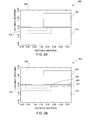
- FIG 2B shows, in partial cross-sectional view, in FIG 2B , and may be further understood with reference to FIG. 2A , which shows, in partial cross-sectional view, a conventional MOSFET.
- FIGs 2A and 2B show a partial cross section of vertical MOSFET 200, comprising drift layer 212, p-doped base or shielding layer 216, n-doped channel layer 218, and in the instance of the inventive device shown in FIG. 2B , p-doped surface layer 220, i.e., channel layer 218 is buried in the inventive device shown in FIG. 2B .
- Each of MOSFETs 200 shown in FIGs 2A and 2B further comprise dielectric 228, gate 222 and passivation layer 224.
- base or shielding layer 216 may be n-doped
- channel layer 218 may be p-doped
- surface layer 220 may be n-doped.
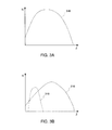
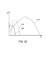
- FIGs 3A-3C are graphical depictions of the logarithmic dopant concentration versus distance from the surface for a conventional device such as that shown in FIG 2A , and a device as described herein. More particularly, FIG. 3A is a graphical depiction of the conventional doping profile of an ion implanted base or shielding layer 316 having a second conductivity type using single or multiple energy sources into a drift layer (not shown) having a first conductivity type in a conventional (inversion mode Double Implanted-MOSFET) device. In the conventional device, the base or shielding layer needs to shield the junction formed by the second and first conductivity type for higher voltages, as well as provide the optimal threshold voltage to form an inversion mode channel region.
- a channel layer 318 of a first conductivity type is ion implanted into the base or shielding layer 316 of the second conductivity type.
- the addition of the channel layer avoids the threshold voltage dependence on the base or shielding layer 316. And so, by adjusting the doping of the channel layer 318, a range of conduction modes are possible, namely, threshold adjusted inversion mode conduction, depletion mode conduction or buried conduction.
- a surface layer 320 of the second conductivity type is provided. With the addition of this surface layer, one can now tailor the device from normally off inversion mode to normally off buried conduction mode, as well as tailoring the devices' transconductance from the typically low values observed in inversion mode to higher values seen in buried channel devices.
- the base or shielding layer, channel, and surface layer are desirably formed via ion implantation.
- Ion implantation allows more control of thickness and/or dopant concentration than other fabrication methods, and as a result, offers more flexibility in charge tradeoff in the present base or shielding layer, channel and surface layer, and thus, more control over the threshold voltage and amount of buried channel conduction.
- ion implantation is a practical fabrication technique already used in many facets of semiconductor manufacture, and as a result, the present methods will be easily implemented in many manufacturing settings.
- a semiconductor structure comprising providing a drift layer having a first conductivity type, and ion implanting thereupon a base or shielding layer having a second conductivity type.
- a channel having the first conductivity type is ion implanted within the base or shielding layer, and a surface layer having the second conductivity type is ion implanted so as to overlie at least a portion of the base or shielding layer.
- FIG. 4 is a graphical representation of calculated drain current density versus gate voltage characteristics of embodiments of the present invention.
- threshold voltage refers to the voltage given by the X-intercept of the linear fit to the drain current versus gate voltage characteristics of a MOSFET device. Transconductance is obtained by differentiating the drain current versus gate voltage characteristics of a MOSFET device.
- Device A comparativative
- Devices B, C, D and E are devices according to embodiments of the invention described herein, wherein a base or shielding layer, channel layer and surface layers are all present in the channel region. All of these devices have the same channel length, i.e. 0.5 ⁇ m.
- Devices D and E have similar base or shielding layer and channel layer dopant concentrations.
- Device E has a higher surface dopant concentration and thus, a higher threshold voltage than device D.
- Devices E and C have similar base or shielding layer and surface layer dopant concentrations. But, device C has a higher channel dopant concentration and thus, a lower threshold voltage than device E.
- Maximum transconductance for the devices C, D and E are 3.7 siemens/cm 2 , 4.3 siemenS/Cm 2 and 4.5 siemens/cm 2 , respectively.
- the dopant concentrations of each layer of the devices according to embodiments of the devices described herein are shown in Table 1, below.
- Device A has an offstate of over 5 V, and a gradual slope indicating low conductance.
- Devices B, C, D and E all give greater transconductance, with Device E giving the greatest threshold voltage, thus illustrating that by utilizing the principles disclosed herein, the off voltage versus transconductance can be tailored depending on the particular desired application.
- each of the base or shielding layer, channel and surface layer may be formed in the same or different apparatus.
- the ion implantation is carried out using p- or n- dopant precursors that are well known to those of ordinary skill in the art.
- a graded layer may be provided, i.e., the concentration of the dopant throughout the thickness of the layer can be caused to vary.
- the surface layer is relatively shallow, low implantation energies may be utilized to form the same, i.e., implantation energies of from about 25keV to about 100keV.
- the surface layer may be implanted through a "screen" oxide layer.
- screen oxides are one example of a sacrificial layer. Such layers have no direct function in the completed structure or device and thus, are typically disposed of after use. In implantation, these oxides are provided at a given thickness to absorb some of the implanted dopants and cause net reduction of the penetration depth of the dopants, thus assisting in shallow implantations.
Landscapes
- Insulated Gate Type Field-Effect Transistor (AREA)
- Recrystallisation Techniques (AREA)
- Carbon And Carbon Compounds (AREA)
- Junction Field-Effect Transistors (AREA)
Abstract
Description
- The present disclosure relates to silicon carbide MOS semiconductor structures and devices, such as a field-effect transistors, and methods of making these.
- Silicon carbide (SiC) inversion mode MOSFETs have very low channel mobilities caused by excessive electron trapping due to SiC/SiO2 interface traps and surface scattering. Instead of achieving the expected value of 250 cm2/v-sec, only 15 to 20 cm2/v-sec are typically achieved in conventional SiC inversion mode MOSFETs.
- Moving to a buried channel FET structure wherein much of the conduction is subsurface can alleviate low mobility problems. However, such devices usually have low threshold voltages between 1 and 3 volts at room temperature - not high enough to provide the desired noise immunity and a "hard" off state, especially at higher temperatures.
- In efforts to provide increased threshold voltages, much research has been focused on higher work function gate materials. For example many buried channel devices utilize heavily doped p+ polysilicon gate electrodes. But this material, even though it has a higher work function than molybdenum or n+ polysilicon, only provides a threshold increase of about 0.4 volts. Further, although the use of, e.g., p+ SiC, or even p type diamond films, as gate electrode materials is expected to increase the threshold by about 1.4 volts and 3 volts respectively, it has yet to be demonstrated that these two complex materials can be properly fabricated to be used as gate electrodes over thin SiO2 gate dielectrics.
- Thus, there remains a need for normally-off buried channel SiC MOSFETs with a sufficiently high threshold voltage for power switching applications. The advantages of such a device could be further leveraged if it could be practically and simply manufactured.
- A silicon carbide semiconductor FET structure is provided. The structure comprises a drift layer having a first conductivity type, an ion implanted base or shielding structure having a second conductivity type overlying at least a portion of the drift layer, an ion implanted channel of the first conductivity type within the base or shielding structure, and an ion implanted surface layer of the second conductivity type overlying at least a portion of the base or shielding structure.
- Also provided are silicon carbide semiconductor devices comprising a semiconductor structure having a drift layer having a first conductivity type, an ion implanted base or shielding structure having a second conductivity type within the first conductivity type, an ion implanted channel of the first conductivity type within the base or shielding structure, and an ion implanted surface layer of the second conductivity type overlying at least a portion of the base or base or shielding structure. The device further comprises a dielectric and then a gate conductor located on a portion of said ion-implanted surface layer and a source region and a drain region, which are in contact with at least said ion-implanted channel.
- Methods of making a semiconductor structure are also provided. The methods comprise providing a drift layer having a first conductivity type and ion implanting a base or shielding layer having a second conductivity type, ion implanting a channel within the base or shielding layer having the first conductivity type, and ion implanting a surface layer overlying at least a portion of the base or base or shielding structure and having the second conductivity type.
- There follows a detailed description of embodiments of the invention by way of example only with reference to the accompanying drawings, in which:
-
FIG. 1 is a cross-sectional view of a semiconductor structure according to one embodiment; -
FIG. 2A is a partial cross-sectional view of a conventional semiconductor device; -
FIG. 2B is a partial cross-sectional view of a semiconductor device according to one embodiment; -
FIG. 3A is a graphical depiction of logarithmic dopant concentration versus the distance from the surface for a conventional semiconductor device; -
FIG. 3B is a graphical depiction of logarithmic dopant concentration versus the distance from the surface for conventional buried channel semiconductor device; -
FIG. 3C is a graphical depiction of logarithmic dopant concentration versus the distance from the surface for a semiconductor device according to one embodiment; and -
FIG 4 is a graphical depiction of the calculated transfer characteristics of MOSFET devices in accordance with one embodiment of the present invention. - Unless defined otherwise, technical and scientific terms used herein have the same meaning as is commonly understood by one of skill in the art to which this invention belongs. The terms "first", "second", and the like, as used herein do not denote any order, quantity, or importance, but rather are used to distinguish one element from another. Also, the terms "a" and "an" do not denote a limitation of quantity, but rather denote the presence of at least one of the referenced item, and the terms "front", "back", "bottom", and/or "top", unless otherwise noted, are merely used for convenience of description, and are not limited to any one position or spatial orientation. If ranges are disclosed, the endpoints of all ranges directed to the same component or property are inclusive and independently combinable (e.g., ranges of "up to about 25 wt.%, or, more specifically, about 5 wt.% to about 20 wt.%," is inclusive of the endpoints and all intermediate values of the ranges of "about 5 wt.% to about 25 wt.%," etc.). The modifier "about" used in connection with a quantity is inclusive of the stated value and has the meaning dictated by the context (e.g., includes the degree of error associated with measurement of the particular quantity).
- It will be understood that when an element such as a layer, region or drift layer is referred to as being "on" or "over" another element, it can be directly on the other element, or, intervening elements may be present. On the other hand, when an element is referred to as being "directly on" or "directly over" another element, there are no intervening elements present. Likewise, when an element is referred to as being "beneath" or "under" another element, it can be directly beneath or under the other element, or intervening elements may be present. In contrast, when an element is referred to as being "directly beneath" or "directly under" another element, there are no intervening elements present.
- There is provided herein a silicon carbide semiconductor structure. The structure comprises a drift layer having a first conductivity type, a base or shielding structure having a second conductivity type overlying at least a portion of the drift layer, a channel of the first conductivity type within the base or shielding structure, and a surface layer of the second conductivity type overlying at least a portion of the base or shielding structure. The base or shielding structure, surface layer and channel are desirably formed via ion implantation, and as a result, and as compared to providing such layers by other methods, such as e.g., by epitaxial growth, very fine control is possible over the thickness and charge concentration of each layer. As a result, the charge tradeoff of these layers may be manipulated to provide the desired threshold voltage and/or amount of buried channel conduction.
- Any p-doped feature(s) within the structure or device may comprise any p-type dopant (i.e., an element from column III of the Periodic table of elements), while the dopant present in any n-doped feature(s) may be any n-type dopant (i.e., an element from column V of the Periodic Table of elements). When more than one feature of the semiconductor structure or device comprises the p-dopant(s), the p-dopant(s) may be the same or different. In certain embodiments, the p-type dopant(s) may comprise, for example, aluminum or boron or combinations of these. Similarly, when more than one features of the semiconductor structure or device comprises the n-dopant(s), the n-dopant(s) may be the same or different. In certain embodiments, the n-type dopant(s) may comprise, for example phosphorous or nitrogen.
- The base or shielding layer will desirably be highly doped, i.e., will comprise a sufficient dopant concentration so that the device has lower reverse leakage current and/or the device will not exhibit substantial punchthrough breakdown at high drain voltages. More particularly, the base or shielding layer will desirably comprise a dopant density of from about 2×1013cm-2 to about 2×1014cm-2, or from about 3×1013cm-2 to about 1.8×1014cm-2, or even from about 7.5×1013cm-2 to about 1.5x1014cm-2. On the other hand, the channel may desirably comprise dopant densities from about 1×1012cm-2 to about 8×1012cm-2, or from about 2×1012cm-2 to about 7.5×1012cm-2, or even from about 2×1012cm-2 to about 7×1012cm-2. Appropriate dopant densities for the surface layer can range from about 1×1011cm-2 to about 4×1012cm-2, or from about 1×1011cm-2 to about 3×1012cm-2, or even from about 1×1011cm-2 to about 2.5×1012cm-2.
- The surface layer, utilized to control the threshold of the device as required to maintain low channel in the offstate, will desirably be relatively shallow, i.e., will be from about 0.05cm to about 0.1µm from the surface of the structure or device so that existing ion implantation technology may advantageously be utilized in forming the surface layer.
- The present semiconductor structure may be further described with reference to one embodiment of the same shown in
FIG. 1 . More particularly,semiconductor structure 100 includesdrift layer 112, appropriate for the voltage range. Lightly dopeddrift layer 112 can be epitaxially deposited, if desired, and has formed thereupon p-doped base orshielding layer 116, an n-dopedchannel layer 118 located on an upper surface of base orshielding layer 116, and a p-dopedsurface layer 120 located on an upper surface of the n-dopedchannel layer 118. - In an alternate embodiment (not shown), base or
shielding layer 116 may be n-doped,channel layer 118 may be p-doped, andsurface layer 120 may be n-doped.Drift layer 112 may comprise any semiconductor material, and desirably comprises silicon carbide.Drift layer 112 may be doped, undoped, or may contain doped and undoped regions therein. - Each of the
individual layers shielding layer 116 will have a thickness of from about 0.1µm to about 0.7 µm, with a thickness of from about 0.25µm to about 0.6µm being more typical.Channel layer 118 of the inventive structure will typically have a thickness of from about 0.05µm to about 0.25µm, or from about 0.1µm to about 0.15µm. The thickness of thesurface layer 120 typically between about 0.05µm and about 0.1µm. Thickness of the surface layer, 120, is defined as the distance from the semiconductor and insulator to metallurgical junction formed by the surface layer and n-channel layer. Thickness of the channel layer, 118, is defined as the distance from the metallurgical junction formed by the surface layer and n-channel layer to the metallurgical junction formed by channel layer and base or shielding layer. Thickness of the base or shielding layer, 116, is defined as the distance from the metallurgical junction formed by the channel layer and base or shielding layer to the metallurgical junction formed by base or shielding layer and the drift layer. - The semiconductor structure described herein may be provided in connection with any other desired components or features in order to make a functioning semiconductor device. It has now been shown that such devices can be normally off, with a high enough threshold voltage (e.g., greater than about 3V, greater than 4V, or even greater than about 5V) to reduce or even substantially prevent off-state channel leakage. Stated another way, devices in accordance with such embodiments allow the device to operate in a buried channel or inversion mode, and/or optimization of the normally-off threshold voltage versus the transconductance.
- For example, the semiconductor structure may be provided in connection with a gate oxide/dielectric and gate conductor and source and drain regions, to form a portion of a lateral or vertical MOSFET, etc. One example of semiconductor device in accordance with this embodiment is shown, in partial cross-sectional view, in
FIG 2B , and may be further understood with reference toFIG. 2A , which shows, in partial cross-sectional view, a conventional MOSFET. - More particularly,
FIGs 2A and 2B show a partial cross section ofvertical MOSFET 200, comprisingdrift layer 212, p-doped base or shieldinglayer 216, n-dopedchannel layer 218, and in the instance of the inventive device shown inFIG. 2B , p-dopedsurface layer 220, i.e.,channel layer 218 is buried in the inventive device shown inFIG. 2B . Each ofMOSFETs 200 shown inFIGs 2A and 2B further comprise dielectric 228,gate 222 andpassivation layer 224. It is expected, that by providingdevice 200 shown in 2B with buriedchannel layer 218 andsurface layer 220, that this device will exhibit enhanced mobilities of from about 60 cm2/V-sec to about 100 cm2/V-sec as compared to mobilities of from about 10 cm2/V-sec to about 15 cm2/V-sec exhibited by conventional inversion mode FET structures or devices, such as that shown inFIG. 2A . As with the disclosed semiconductor structure, in an additional embodiment of the present semiconductor device, base or shieldinglayer 216 may be n-doped,channel layer 218 may be p-doped, andsurface layer 220 may be n-doped. -
FIGs 3A-3C are graphical depictions of the logarithmic dopant concentration versus distance from the surface for a conventional device such as that shown inFIG 2A , and a device as described herein. More particularly,FIG. 3A is a graphical depiction of the conventional doping profile of an ion implanted base or shieldinglayer 316 having a second conductivity type using single or multiple energy sources into a drift layer (not shown) having a first conductivity type in a conventional (inversion mode Double Implanted-MOSFET) device. In the conventional device, the base or shielding layer needs to shield the junction formed by the second and first conductivity type for higher voltages, as well as provide the optimal threshold voltage to form an inversion mode channel region. - In
FIG 3B , achannel layer 318 of a first conductivity type is ion implanted into the base or shieldinglayer 316 of the second conductivity type. The addition of the channel layer, avoids the threshold voltage dependence on the base or shieldinglayer 316. And so, by adjusting the doping of thechannel layer 318, a range of conduction modes are possible, namely, threshold adjusted inversion mode conduction, depletion mode conduction or buried conduction. - In
Figure 3C , asurface layer 320 of the second conductivity type is provided. With the addition of this surface layer, one can now tailor the device from normally off inversion mode to normally off buried conduction mode, as well as tailoring the devices' transconductance from the typically low values observed in inversion mode to higher values seen in buried channel devices. - As mentioned above, the base or shielding layer, channel, and surface layer are desirably formed via ion implantation. Ion implantation allows more control of thickness and/or dopant concentration than other fabrication methods, and as a result, offers more flexibility in charge tradeoff in the present base or shielding layer, channel and surface layer, and thus, more control over the threshold voltage and amount of buried channel conduction. Also, ion implantation is a practical fabrication technique already used in many facets of semiconductor manufacture, and as a result, the present methods will be easily implemented in many manufacturing settings.
- As such, also provided herein are methods for making a semiconductor structure comprising providing a drift layer having a first conductivity type, and ion implanting thereupon a base or shielding layer having a second conductivity type. A channel having the first conductivity type is ion implanted within the base or shielding layer, and a surface layer having the second conductivity type is ion implanted so as to overlie at least a portion of the base or shielding layer.
-
FIG. 4 is a graphical representation of calculated drain current density versus gate voltage characteristics of embodiments of the present invention. As used herein, the term "threshold voltage" refers to the voltage given by the X-intercept of the linear fit to the drain current versus gate voltage characteristics of a MOSFET device. Transconductance is obtained by differentiating the drain current versus gate voltage characteristics of a MOSFET device. Device A (comparative) is an inversion mode device where is only p-well layer is present in the channel. Devices B, C, D and E are devices according to embodiments of the invention described herein, wherein a base or shielding layer, channel layer and surface layers are all present in the channel region. All of these devices have the same channel length, i.e. 0.5µm. Devices D and E have similar base or shielding layer and channel layer dopant concentrations. - Device E has a higher surface dopant concentration and thus, a higher threshold voltage than device D. Devices E and C have similar base or shielding layer and surface layer dopant concentrations. But, device C has a higher channel dopant concentration and thus, a lower threshold voltage than device E. Maximum transconductance for the devices C, D and E are 3.7 siemens/cm2, 4.3 siemenS/Cm2 and 4.5 siemens/cm2, respectively. The dopant concentrations of each layer of the devices according to embodiments of the devices described herein are shown in Table 1, below.
TABLE 1 Device Pshielding Nchannel Psurface A (Comparative) -- -- -- B 9e13/cm2 3e12/cm2 1e12/cm2 C 12e13/cm2 6e12/cm2 2.25e12/cm2 D 12e13/cm2 3e12/cm2 1e12/cm2 E 12e13/cm2 3e12/cm2 2.25e12/cm2 - As shown in
FIG. 4 , Device A has an offstate of over 5 V, and a gradual slope indicating low conductance. In contrast, Devices B, C, D and E all give greater transconductance, with Device E giving the greatest threshold voltage, thus illustrating that by utilizing the principles disclosed herein, the off voltage versus transconductance can be tailored depending on the particular desired application. - The deposition of each of the base or shielding layer, channel and surface layer may be formed in the same or different apparatus. The ion implantation is carried out using p- or n- dopant precursors that are well known to those of ordinary skill in the art. In some embodiments, a graded layer may be provided, i.e., the concentration of the dopant throughout the thickness of the layer can be caused to vary.
- Further, because the surface layer is relatively shallow, low implantation energies may be utilized to form the same, i.e., implantation energies of from about 25keV to about 100keV. Or, the surface layer may be implanted through a "screen" oxide layer. Well known to those of ordinary skill in the art, screen oxides are one example of a sacrificial layer. Such layers have no direct function in the completed structure or device and thus, are typically disposed of after use. In implantation, these oxides are provided at a given thickness to absorb some of the implanted dopants and cause net reduction of the penetration depth of the dopants, thus assisting in shallow implantations.
- While only certain features of the invention have been illustrated and described herein, many modifications and changes will occur to those skilled in the art. It is, therefore, to be understood that the appended claims are intended to cover all such modifications and changes as fall within the true spirit of the invention.
Claims (15)
- A silicon carbide semiconductor FET structure (100) comprising a drift layer (112) having a first conductivity type, an ion implanted base or shielding structure (116) having a second conductivity type within the drift layer, an ion implanted channel (118) of the first conductivity type within the base or shielding structure (116), and an ion implanted surface layer (120) of the second conductivity type overlying at least a portion of the base or shielding structure (116).
- The silicon carbide semiconductor structure of claim 1, wherein the base or shielding layer comprises a dopant density of from about 2×1013cm-2 to about 2×1014cm-2.
- The silicon carbide semiconductor structure of claim 2, wherein the base or shielding layer comprises a dopant density of from about 7.5×1013cm-2 to about 1.5c1014cm-2.
- The silicon carbide semiconductor structure of claim 1, wherein the dopant utilized in the base or shielding layer and the surface layer are the same.
- The silicon carbide semiconductor structure of claim 1, wherein the dopant utilized in the base or shielding layer and the surface layer are different.
- The silicon carbide semiconductor structure of claim 1, wherein the dopant utilized in the base or shielding layer and/or the surface layer comprises aluminum or boron.
- The silicon carbide semiconductor structure of claim 1, wherein the channel comprises a dopant concentration of from about 1×1011cm-2 to about 8×1012cm-2 atoms/cm2.
- The silicon carbide semiconductor structure of claim 5, wherein the dopant utilized in the ion-implanted n-doped channel comprises phosphorous or nitrogen.
- A silicon carbide semiconductor device (200) comprising:a drift layer (212) having a first conductivity type and having an upper surface;a structure comprising an ion implanted base or shielding structure (216) within the drift layer (212) having a second conductivity type, an ion implanted channel (218) of the first conductivity type within the base or shielding structure (216), and an ion implanted surface layer (220) of the second conductivity type overlying at least a portion of the base or shielding structure (216);a dielectric (228) located on a portion of said surface layer (220);a gate conductor (222) overlying at least a portion of the dielectric (228); anda source contact and a drain contact which are in contact with at least said channel.
- The silicon carbide semiconductor device of claim 9, wherein the base or shielding layer comprises a dopant density of from about 2×1013cm-2 to about 2×1014cm-2.
- The silicon carbide semiconductor device of claim 9 or 10, having a threshold voltage of greater than about 3 volts.
- The silicon carbide semiconductor device of any of claims 9 to 11, wherein the device is capable of operating in either buried channel or inversion mode and wherein the normally off threshold voltage versus the transconductance can be tailored.
- A vertical or lateral MOSFET comprising the silicon carbide semiconductor structure of claim 9.
- A method of making a semiconductor structure comprising providing a drift layer having a first conductivity type, ion implanting a base or shielding layer having a second conductivity type overlying at least a portion of the drift layer, ion implanting a channel having the first conductivity type within the base or shielding layer and ion implanting a surface layer having the second conductivity type so that the surface layer overlies at least a portion of the base or shielding structure.
- The method of claim 14, wherein the surface layer is implanted using implantation energies of from about 25keV to about 100keV
Applications Claiming Priority (1)
| Application Number | Priority Date | Filing Date | Title |
|---|---|---|---|
| US12/533,712 US20110024765A1 (en) | 2009-07-31 | 2009-07-31 | Silicon carbide semiconductor structures, devices and methods for making the same |
Publications (2)
| Publication Number | Publication Date |
|---|---|
| EP2282348A2 true EP2282348A2 (en) | 2011-02-09 |
| EP2282348A3 EP2282348A3 (en) | 2012-09-05 |
Family
ID=42941825
Family Applications (1)
| Application Number | Title | Priority Date | Filing Date |
|---|---|---|---|
| EP10171439A Withdrawn EP2282348A3 (en) | 2009-07-31 | 2010-07-30 | Silicon carbide semiconductor structures, devices, and methods for making the same |
Country Status (6)
| Country | Link |
|---|---|
| US (1) | US20110024765A1 (en) |
| EP (1) | EP2282348A3 (en) |
| JP (1) | JP2011035394A (en) |
| CN (1) | CN101989615A (en) |
| BR (1) | BRPI1002783A2 (en) |
| CA (1) | CA2711066A1 (en) |
Families Citing this family (3)
| Publication number | Priority date | Publication date | Assignee | Title |
|---|---|---|---|---|
| US9246019B2 (en) * | 2010-12-17 | 2016-01-26 | Diodes Incorporated | High efficiency rectifier |
| US10367089B2 (en) * | 2011-03-28 | 2019-07-30 | General Electric Company | Semiconductor device and method for reduced bias threshold instability |
| CN109585541B (en) * | 2018-12-27 | 2024-03-26 | 西安中车永电电气有限公司 | Buried channel type SiC IGBT normally-off device and preparation method thereof |
Family Cites Families (18)
| Publication number | Priority date | Publication date | Assignee | Title |
|---|---|---|---|---|
| US5543637A (en) * | 1994-11-14 | 1996-08-06 | North Carolina State University | Silicon carbide semiconductor devices having buried silicon carbide conduction barrier layers therein |
| SE9800286D0 (en) * | 1998-02-02 | 1998-02-02 | Abb Research Ltd | A transistor of SiC |
| US6107649A (en) * | 1998-06-10 | 2000-08-22 | Rutgers, The State University | Field-controlled high-power semiconductor devices |
| JP3666280B2 (en) * | 1999-01-20 | 2005-06-29 | 富士電機ホールディングス株式会社 | Silicon carbide vertical FET and method of manufacturing the same |
| JP4192353B2 (en) * | 1999-09-21 | 2008-12-10 | 株式会社デンソー | Silicon carbide semiconductor device and manufacturing method thereof |
| US6956238B2 (en) * | 2000-10-03 | 2005-10-18 | Cree, Inc. | Silicon carbide power metal-oxide semiconductor field effect transistors having a shorting channel and methods of fabricating silicon carbide metal-oxide semiconductor field effect transistors having a shorting channel |
| JP3940560B2 (en) * | 2001-01-25 | 2007-07-04 | 独立行政法人産業技術総合研究所 | Manufacturing method of semiconductor device |
| JP3800047B2 (en) * | 2001-07-18 | 2006-07-19 | 日産自動車株式会社 | Field effect transistor |
| JP3520346B2 (en) * | 2001-08-21 | 2004-04-19 | 株式会社東芝 | Semiconductor device |
| KR20050084685A (en) * | 2002-11-25 | 2005-08-26 | 도꾸리쯔교세이호진 상교기쥬쯔 소고겡뀨죠 | Semiconductor device and power converter, driving inverter, general-purpose inverter and high-power high-frequency communication device using same |
| US20050012143A1 (en) * | 2003-06-24 | 2005-01-20 | Hideaki Tanaka | Semiconductor device and method of manufacturing the same |
| JP4564362B2 (en) * | 2004-01-23 | 2010-10-20 | 株式会社東芝 | Semiconductor device |
| US7407837B2 (en) * | 2004-01-27 | 2008-08-05 | Fuji Electric Holdings Co., Ltd. | Method of manufacturing silicon carbide semiconductor device |
| JP4604241B2 (en) * | 2004-11-18 | 2011-01-05 | 独立行政法人産業技術総合研究所 | Silicon carbide MOS field effect transistor and manufacturing method thereof |
| JP4903439B2 (en) * | 2005-05-31 | 2012-03-28 | 株式会社東芝 | Field effect transistor |
| US20070126007A1 (en) * | 2005-12-07 | 2007-06-07 | Matocha Kevin S | SiC semiconductor device and method of fabricating same |
| JP4545800B2 (en) * | 2006-02-07 | 2010-09-15 | 三菱電機株式会社 | Silicon carbide semiconductor device and manufacturing method thereof |
| US7595241B2 (en) * | 2006-08-23 | 2009-09-29 | General Electric Company | Method for fabricating silicon carbide vertical MOSFET devices |
-
2009
- 2009-07-31 US US12/533,712 patent/US20110024765A1/en not_active Abandoned
-
2010
- 2010-07-28 JP JP2010168721A patent/JP2011035394A/en not_active Withdrawn
- 2010-07-29 CA CA2711066A patent/CA2711066A1/en not_active Abandoned
- 2010-07-30 BR BRPI1002783-1A patent/BRPI1002783A2/en not_active Application Discontinuation
- 2010-07-30 EP EP10171439A patent/EP2282348A3/en not_active Withdrawn
- 2010-08-02 CN CN2010102519819A patent/CN101989615A/en active Pending
Non-Patent Citations (1)
| Title |
|---|
| None |
Also Published As
| Publication number | Publication date |
|---|---|
| BRPI1002783A2 (en) | 2012-03-27 |
| JP2011035394A (en) | 2011-02-17 |
| CN101989615A (en) | 2011-03-23 |
| US20110024765A1 (en) | 2011-02-03 |
| CA2711066A1 (en) | 2011-01-31 |
| EP2282348A3 (en) | 2012-09-05 |
Similar Documents
| Publication | Publication Date | Title |
|---|---|---|
| US10727334B2 (en) | Lateral DMOS device with dummy gate | |
| US8362550B2 (en) | Trench power MOSFET with reduced on-resistance | |
| CN100524809C (en) | A field effect transistor semiconductor device | |
| US11610968B2 (en) | LDMOS transistor and method of forming the LDMOS transistor with improved Rds*Cgd | |
| US10355123B2 (en) | Silicon-carbide trench gate MOSFETs and methods of manufacture | |
| JP5586887B2 (en) | Semiconductor device and manufacturing method thereof | |
| US7705396B2 (en) | Trench type MOSFET and method of fabricating the same | |
| US6323506B1 (en) | Self-aligned silicon carbide LMOSFET | |
| JPWO2005083796A1 (en) | Semiconductor device and manufacturing method thereof | |
| US11063115B2 (en) | Semiconductor device and method of making thereof | |
| JP2020126932A (en) | Trench gate type semiconductor device | |
| WO2023095363A1 (en) | Semiconductor device and method for manufacturing same | |
| TW202234712A (en) | Sic mosfet with reduced channel length and high vth | |
| CN113424327B (en) | Systems and methods for unipolar charge-balanced semiconductor power devices | |
| EP2282348A2 (en) | Silicon carbide semiconductor structures, devices, and methods for making the same | |
| US12302612B2 (en) | And manufacture of robust, high-performance devices | |
| JP2003518749A (en) | Silicon carbide LMOSFET with gate breakdown protection | |
| US10811494B2 (en) | Method and assembly for mitigating short channel effects in silicon carbide MOSFET devices | |
| US20230352520A1 (en) | Wide band gap semiconductor device | |
| JP2025510198A (en) | Power semiconductor device with shallow conduction region - Patents.com | |
| WO2019094338A1 (en) | Method and assembly for mitigating short channel effects in silicon carbide mosfet devices |
Legal Events
| Date | Code | Title | Description |
|---|---|---|---|
| PUAI | Public reference made under article 153(3) epc to a published international application that has entered the european phase |
Free format text: ORIGINAL CODE: 0009012 |
|
| AK | Designated contracting states |
Kind code of ref document: A2 Designated state(s): AL AT BE BG CH CY CZ DE DK EE ES FI FR GB GR HR HU IE IS IT LI LT LU LV MC MK MT NL NO PL PT RO SE SI SK SM TR |
|
| AX | Request for extension of the european patent |
Extension state: BA ME RS |
|
| PUAL | Search report despatched |
Free format text: ORIGINAL CODE: 0009013 |
|
| AK | Designated contracting states |
Kind code of ref document: A3 Designated state(s): AL AT BE BG CH CY CZ DE DK EE ES FI FR GB GR HR HU IE IS IT LI LT LU LV MC MK MT NL NO PL PT RO SE SI SK SM TR |
|
| AX | Request for extension of the european patent |
Extension state: BA ME RS |
|
| RIC1 | Information provided on ipc code assigned before grant |
Ipc: H01L 29/06 20060101ALI20120730BHEP Ipc: H01L 29/78 20060101AFI20120730BHEP Ipc: H01L 29/16 20060101ALN20120730BHEP |
|
| 17P | Request for examination filed |
Effective date: 20130305 |
|
| D17P | Request for examination filed (deleted) | ||
| STAA | Information on the status of an ep patent application or granted ep patent |
Free format text: STATUS: THE APPLICATION IS DEEMED TO BE WITHDRAWN |
|
| 18D | Application deemed to be withdrawn |
Effective date: 20130321 |