EP2282307A1 - Organic light emitting display device and driving voltage setting method thereof - Google Patents
Organic light emitting display device and driving voltage setting method thereof Download PDFInfo
- Publication number
- EP2282307A1 EP2282307A1 EP10155924A EP10155924A EP2282307A1 EP 2282307 A1 EP2282307 A1 EP 2282307A1 EP 10155924 A EP10155924 A EP 10155924A EP 10155924 A EP10155924 A EP 10155924A EP 2282307 A1 EP2282307 A1 EP 2282307A1
- Authority
- EP
- European Patent Office
- Prior art keywords
- driving voltage
- light emitting
- voltage
- organic light
- panel
- Prior art date
- Legal status (The legal status is an assumption and is not a legal conclusion. Google has not performed a legal analysis and makes no representation as to the accuracy of the status listed.)
- Granted
Links
- 238000000034 method Methods 0.000 title claims description 15
- 239000003086 colorant Substances 0.000 claims description 5
- 238000005259 measurement Methods 0.000 abstract 1
- 239000003990 capacitor Substances 0.000 description 6
- 238000010586 diagram Methods 0.000 description 4
- 230000001419 dependent effect Effects 0.000 description 1
- 238000005516 engineering process Methods 0.000 description 1
- 239000000463 material Substances 0.000 description 1
- 150000002894 organic compounds Chemical class 0.000 description 1
Images

Classifications
-
- G—PHYSICS
- G09—EDUCATION; CRYPTOGRAPHY; DISPLAY; ADVERTISING; SEALS
- G09G—ARRANGEMENTS OR CIRCUITS FOR CONTROL OF INDICATING DEVICES USING STATIC MEANS TO PRESENT VARIABLE INFORMATION
- G09G3/00—Control arrangements or circuits, of interest only in connection with visual indicators other than cathode-ray tubes
- G09G3/20—Control arrangements or circuits, of interest only in connection with visual indicators other than cathode-ray tubes for presentation of an assembly of a number of characters, e.g. a page, by composing the assembly by combination of individual elements arranged in a matrix no fixed position being assigned to or needed to be assigned to the individual characters or partial characters
- G09G3/22—Control arrangements or circuits, of interest only in connection with visual indicators other than cathode-ray tubes for presentation of an assembly of a number of characters, e.g. a page, by composing the assembly by combination of individual elements arranged in a matrix no fixed position being assigned to or needed to be assigned to the individual characters or partial characters using controlled light sources
- G09G3/30—Control arrangements or circuits, of interest only in connection with visual indicators other than cathode-ray tubes for presentation of an assembly of a number of characters, e.g. a page, by composing the assembly by combination of individual elements arranged in a matrix no fixed position being assigned to or needed to be assigned to the individual characters or partial characters using controlled light sources using electroluminescent panels
- G09G3/32—Control arrangements or circuits, of interest only in connection with visual indicators other than cathode-ray tubes for presentation of an assembly of a number of characters, e.g. a page, by composing the assembly by combination of individual elements arranged in a matrix no fixed position being assigned to or needed to be assigned to the individual characters or partial characters using controlled light sources using electroluminescent panels semiconductive, e.g. using light-emitting diodes [LED]
- G09G3/3208—Control arrangements or circuits, of interest only in connection with visual indicators other than cathode-ray tubes for presentation of an assembly of a number of characters, e.g. a page, by composing the assembly by combination of individual elements arranged in a matrix no fixed position being assigned to or needed to be assigned to the individual characters or partial characters using controlled light sources using electroluminescent panels semiconductive, e.g. using light-emitting diodes [LED] organic, e.g. using organic light-emitting diodes [OLED]
- G09G3/3225—Control arrangements or circuits, of interest only in connection with visual indicators other than cathode-ray tubes for presentation of an assembly of a number of characters, e.g. a page, by composing the assembly by combination of individual elements arranged in a matrix no fixed position being assigned to or needed to be assigned to the individual characters or partial characters using controlled light sources using electroluminescent panels semiconductive, e.g. using light-emitting diodes [LED] organic, e.g. using organic light-emitting diodes [OLED] using an active matrix
- G09G3/3233—Control arrangements or circuits, of interest only in connection with visual indicators other than cathode-ray tubes for presentation of an assembly of a number of characters, e.g. a page, by composing the assembly by combination of individual elements arranged in a matrix no fixed position being assigned to or needed to be assigned to the individual characters or partial characters using controlled light sources using electroluminescent panels semiconductive, e.g. using light-emitting diodes [LED] organic, e.g. using organic light-emitting diodes [OLED] using an active matrix with pixel circuitry controlling the current through the light-emitting element
-
- G—PHYSICS
- G09—EDUCATION; CRYPTOGRAPHY; DISPLAY; ADVERTISING; SEALS
- G09G—ARRANGEMENTS OR CIRCUITS FOR CONTROL OF INDICATING DEVICES USING STATIC MEANS TO PRESENT VARIABLE INFORMATION
- G09G3/00—Control arrangements or circuits, of interest only in connection with visual indicators other than cathode-ray tubes
- G09G3/20—Control arrangements or circuits, of interest only in connection with visual indicators other than cathode-ray tubes for presentation of an assembly of a number of characters, e.g. a page, by composing the assembly by combination of individual elements arranged in a matrix no fixed position being assigned to or needed to be assigned to the individual characters or partial characters
-
- G—PHYSICS
- G09—EDUCATION; CRYPTOGRAPHY; DISPLAY; ADVERTISING; SEALS
- G09G—ARRANGEMENTS OR CIRCUITS FOR CONTROL OF INDICATING DEVICES USING STATIC MEANS TO PRESENT VARIABLE INFORMATION
- G09G2300/00—Aspects of the constitution of display devices
- G09G2300/08—Active matrix structure, i.e. with use of active elements, inclusive of non-linear two terminal elements, in the pixels together with light emitting or modulating elements
- G09G2300/0809—Several active elements per pixel in active matrix panels
- G09G2300/0842—Several active elements per pixel in active matrix panels forming a memory circuit, e.g. a dynamic memory with one capacitor
-
- G—PHYSICS
- G09—EDUCATION; CRYPTOGRAPHY; DISPLAY; ADVERTISING; SEALS
- G09G—ARRANGEMENTS OR CIRCUITS FOR CONTROL OF INDICATING DEVICES USING STATIC MEANS TO PRESENT VARIABLE INFORMATION
- G09G2320/00—Control of display operating conditions
- G09G2320/02—Improving the quality of display appearance
- G09G2320/029—Improving the quality of display appearance by monitoring one or more pixels in the display panel, e.g. by monitoring a fixed reference pixel
-
- G—PHYSICS
- G09—EDUCATION; CRYPTOGRAPHY; DISPLAY; ADVERTISING; SEALS
- G09G—ARRANGEMENTS OR CIRCUITS FOR CONTROL OF INDICATING DEVICES USING STATIC MEANS TO PRESENT VARIABLE INFORMATION
- G09G2320/00—Control of display operating conditions
- G09G2320/04—Maintaining the quality of display appearance
- G09G2320/043—Preventing or counteracting the effects of ageing
-
- G—PHYSICS
- G09—EDUCATION; CRYPTOGRAPHY; DISPLAY; ADVERTISING; SEALS
- G09G—ARRANGEMENTS OR CIRCUITS FOR CONTROL OF INDICATING DEVICES USING STATIC MEANS TO PRESENT VARIABLE INFORMATION
- G09G2330/00—Aspects of power supply; Aspects of display protection and defect management
- G09G2330/02—Details of power systems and of start or stop of display operation
- G09G2330/021—Power management, e.g. power saving
Abstract
Description
- The field relates to an organic light emitting display device and a method of setting a driving voltage thereof, and more particularly, to an organic light emitting display device and method resulting in reduced power.
- Various flat panel display devices that have light weight and small volume when compared to a cathode ray tube have been developed. Among the flat panel display devices, an organic light emitting display device, which uses an organic compound as light emitting material, has various advantages in view of brightness and color purity so that it has been viewed as a next generation display device.
- The organic light emitting display device as described above is coupled between supply linens of high power voltage and low power voltage and use organic light emitting diodes OLED emitting light of a brightness corresponding to data signals to display an image.
- In order to allow the organic light emitting diodes to emit light uniformly during the emission periods of each frame, the voltage difference between the high power voltage and the low power voltage, that is, a driving voltage, should be sufficiently stable.
- To this end, in the general organic light emitting display device, the driving voltage is set, having a voltage margin of about 30%, so that the sufficient driving voltage is determined based on the fluctuation in the driving voltage by the temperature characteristics of the organic light emitting diodes themselves and on the deviation in the driving voltage according to the emission colors.
- However, the organic light emitting display device is typically operated according to an assumed condition. Therefore, the conventional voltage margin set by considering all conditions including even unnecessary conditions leads to unnecessary power consumption, thereby causing an unnecessary increase in power consumption.
- A first aspect of the invention provides a driving method for an organic light emitting display device as set forth in claim 1. A second aspect of the invention provides an organic light emitting display device carrying out the driving method of the first inventive aspect. Preferred embodiments are subject of the dependent claims.
- The accompanying drawings, together with the written description illustrate exemplary embodiments.
-
FIG. 1 is a circuit view showing one example of a pixel according to some embodiments; -
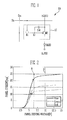
FIG. 2 is a graph showing a panel current according to a driving voltage of a panel; -
FIG. 3 is a block diagram showing an organic light emitting display device according to some embodiments; and -
FIG. 4 is a block diagram showing an example of the current detector ofFIG. 3 . - Hereinafter, certain exemplary embodiments will be described with reference to the accompanying drawings. Herein, when a first element is described as being coupled to a second element, the first element may be directly coupled to the second element or may be indirectly coupled to the second element via a third element. Further, some of the elements that are not essential to the complete understanding of the invention are omitted for clarity. Also, like reference numerals generally refer to like elements throughout.
- Hereinafter, exemplary embodiments will be described with reference to the accompanying drawings.
-
FIG, 1 is a circuit view showing one example of a pixel according to some embodiments. For convenience of explanation, a pixel of an active type organic light emitting display device having a simple structure will be exemplified inFIG. 1 . - Referring to
FIG. 1 , thepixel 10 includes an organic light emitting diode OLED coupled between a supply line of first power voltage ELVDD and a supply line of second power supply ELVSS and apixel circuit 12 that controls the organic light emitting diode OLED. - In this embodiment, the anode electrode of the organic light emitting diode OLED is coupled to the supply line of the first power supply ELVDD via the
pixel circuit 12 and the cathode electrode thereof is coupled to the supply line of the second power supply ELVSS. Herein, the first power voltage ELVDD is a high power voltage and the second power voltage ELVSS is a low power voltage lower than the first power voltage ELVDD. - The organic light emitting diode OLED as described above emits light at a brightness corresponding to the driving current supplied from the
pixel circuit 12. - The
pixel circuit 12 includes a first transistor M1, a second transistor M2, and a capacitor C1. - The first transistor M1 is coupled between a data line Dm and a first node N1, wherein the gate electrode of the first transistor M1 is coupled to a scan line Sn. When a scan signal is supplied from the scan line Sn, the first transistor M1 is turned on to transfer the data signal from the data line Dm to the first node N1.
- The second transistor M2 is coupled between the supply line of the first power voltage ELVDD and the organic light emitting diode OLED, wherein the gate electrode of the second transistor M2 is coupled to the first node N1. The second transistor M2 as described above supplies the driving current corresponding to the voltage Vgs between the source electrode and the gate electrode thereof to the organic light emitting diode OLED.
- The capacitor Cst is coupled between the first node N1 and the supply line of the first power voltage ELVDD. In other words, the capacitor Cst is coupled between the source electrode and the gate electrode of the second transistor M2. When the scan signal is supplied from the scan line Sn, the capacitor Cst is charged with the voltage corresponding to the data signal at the first node N1 to store it for one frame.
- When the scan signal is supplied from the scan line Sn, the first transistor M1 is turned on and the data signal is transferred to the first node N1 from the data line Dm. At this time, the capacitor Cst is charged with the voltage corresponding to the difference between the data signal and the first power voltage ELVDD to store it until the data signal of the next frame is supplied.
- The second transistor M2 acts as a constant current source supplying current corresponding to the data signal to the organic light emitting diode OLED, according to the voltage Vgs between the gate electrode and the source electrode thereof as maintained by the capacitor Cst. Accordingly, the organic light emitting diode OLED emits light at the brightness corresponding to the data signal.
- In order that the organic light emitting diode OLED uniformly emits light according to the data signal during the emission periods of the respective frames, the second transistor M2 is to be a stable constant current source during the emission period of each frame.
- To this end, not only the voltage Vgs between the gate electrode and the source electrode of the second transistor M2 but also the voltage Vds between the source electrode and the drain electrode are to be stable. Therefore, the voltage difference between the high power voltage and the low power voltage, that is, the driving voltage, is to be stable from frame to frame while the panel is driven.
- For a given Vgs, a driving voltage, or Vds can be selected for stable, power efficient operation. A driving voltage which is too low causes high dependence of the driving current on the Vds. That is, for a small change in Vds a large current change occurs. This results in undesired brightness variation. A driving voltage which is too high results in unnecessarily high power consumption. Therefore, some embodiments include a method to reduce power consumption by setting a driving voltage that results in low power driving current which is substantially independent of variation in Vds. The detailed description thereof will be described below.
-
FIG. 2 is a graph showing a panel current according to a driving voltage of a panel. InFIG. 2 , the driving voltage of the panel is the voltage difference between the first power voltage ELVDD and the second power voltage ELVSS and the panel current represents the total amount of current flowing through the panel light emitting diodes. - Referring to
FIG. 2 , for low driving voltages, as the driving voltage of the panel is increased, the amount of current flowing on the panel is also increased. However, in the voltage region greater than a certain driving voltage, the current is substantially constant. - An optimal driving voltage can reduce unnecessary voltage margin, while securing substantially constant current of the driving transistor. In some embodiments, an optimal driving voltage may be selected as the voltage at which the slope of the current vs. driving voltage curve is less than a threshold. The optimal driving voltage may be used as the driving voltage that drives the organic light emitting display device.
- In some embodiments, an optimal driving voltage may be obtained by detecting the driving voltage at the current at a turning point where the derivatives of the panel current according to the driving voltage is changed.
- In some embodiments, the optimal driving voltage for each of the respective emission colors is different. In such embodiments, the highest of the optimal driving voltages may be selected as a single optimal driving voltage for all colors.
- In
FIG. 2 , the points marked with stars are the points where the respective emission colors emit light at desired brightness (for example, brightness of 350cd/m2), the driving voltage at A may be selected as the optimal driving voltage. In this case, the unnecessary power consumption due to the unnecessary voltage margin of approximately 30% of the driving voltage at B is not necessary. - As a result, low voltage can be used for low power, while still achieving substantially constant current. Beneficially, the value of A may be determined while operating the display. The detailed description thereof will be described later with reference to
FIGS. 3 and 4 . -
FIG. 3 is a block diagram showing an organic light emitting display device according to some embodiments, andFIG. 4 is a block diagram showing an example of the current detector ofFIG. 3 . - Referring to
FIG. 3 , the organic light emitting display device includes adisplay panel 100 that display an image, apower supplier 110 that supplies a driving voltage to thedisplay panel 100, and acurrent detector 120 that detects a panel current flowing into thedisplay panel 100 according to the driving voltage. - The
display panel 100 may be implemented as an active type organic light emitting display panel that includes pixels as shown inFIG. 1 or active type pixels having a pixel structure that is variously modified, or a passive type organic light emitting display panel that does not include active elements in the pixel. Also, thedisplay panel 100 may further include a driving circuit such as a scan driver and/or a data driver, etc., according to the design scheme thereof. - The
display panel 100 as described above is turned on by the driving voltage supplied from thepower supplier 110, to display an image corresponding to a data signal. - The
power supplier 110 supplies the driving voltage to thedisplay panel 100. More specifically, thepower supplier 110 outputs a first power voltage ELVDD to a positive output terminal and outputs a second power voltage ELVSS to a negative output terminal. Accordingly, thedisplay panel 100 is driven by the driving voltage, which is the voltage difference between the first power voltage ELVDD and the second power voltage ELVSS. - In some embodiments, the
power supplier 110 includes a variable circuit (not shown) that varies the driving voltage so that the optimal driving voltage is used. For example, thepower supplier 110 may include a variable circuit that varies the driving voltage by varying the first power voltage ELVDD. - The
current detector 120 detects a panel current flowing into thedisplay panel 100 while the driving voltage is supplied from thepower supplier 110 to thedisplay panel 100. For example, thecurrent detector 120 is positioned on the first power supply line that transfers the first power voltage ELVDD from thepower supplier 110 to thedisplay panel 100 to measure the current flowing in the first power supply line, thereby making it possible to detect the panel current flowing into thedisplay panel 100. - The
current detector 120 calculates the variations of the panel current according to the driving voltage, thereby allowing the optimal driving voltage as shown in the time point A inFIG. 2 to be selected. - As shown in
FIG. 4 , thecurrent detector 120 may include acurrent sensor 122 that detects the panel current Ipanel flowing to the display panel and avariation calculator 124 that calculates the variations of the panel current. Also, thecurrent detector 120 may further include acontrol signal generator 126 that controls thepower supplier 110 based on the variations dIpanel of the panel current calculated by thevariation calculator 124. - Accordingly, the
current sensor 122 detects the panel current Ipanel flowing to the display panel while the driving voltage is supplied to thedisplay panel 100. A signal based on the panel current Ipanel detected from thecurrent sensor 122 is input to thevariation calculator 124. - The
variation calculator 124 calculates the variations of the panel current according to the driving voltage. The derivatives of the panel current may be calculated. Accordingly, thevariation calculator 124 may output the derivative of the panel current according to the driving voltage and may, for example, be an analog differentiator. The information on the variations of the panel current calculated from thevariation calculator 124 is input into thecontrol signal generator 126. - The
control signal generator 126 generates a control signal CS that controls thepower supplier 110 according to the variations of the panel current. For example, thecontrol signal generator 126 may generate a control signal so that thepower supplier 110 generates a driving voltage substantially equal to the lowest driving voltage where the derivative of the panel current according to the driving voltage is less than a threshold. - In some embodiments, the
control signal generator 126 is included in thecurrent detector 120, but thecontrol signal generator 126 may be separate from thecurrent detector 120 or may also be in an output voltage setting block in thepower supplier 110. - The organic light emitting display device according to some embodiments varies the driving voltage output into the
display panel 100 from thepower supplier 110 to detect the panel current Ipanel flowing into thedisplay panel 100 and to calculate the variations of the panel current according to the driving voltage, in order to set an optimal driving voltage. - A method of setting a driving voltage for an organic light emitting display device according to some embodiments includes varying a driving voltage in a
power supplier 110 and supplying it to adisplay panel 100, detecting a panel current Ipanel flowing into thedisplay panel 100 during a period when the driving voltage is varied and supplied, and calculating the variations of the panel current according to the driving voltage and setting an optimal driving voltage based on the variations. - An optimal driving voltage may be set as the driving voltage at the point where the driving voltage at a turning point where the derivatives of the panel current according to the driving voltage is changed. (e.g. the driving voltage at the point where the derivative of the panel current is reduced as the driving voltage is increased).
- In some embodiments, the
display panel 100 displays an image while the current and driving voltage data is taken. - In some embodiments, the
display panel 100 displays an image of maximum luminance while the current and driving voltage data is taken. However, the embodiment is not limited thereto. The data can be taken while a still screen is displayed. The display panel does not always set the optimal driving voltage while displaying a full-white screen. For example, after detecting the optimal driving voltage for each emission color, the driving voltage to drive the organic light emitting display device may be finally determined based thereon. Also, in the case of the passive type organic light emitting display device, after detecting the optimal driving voltage for each emission color, the driving voltage optimized for each emission color may be applied at the time of driving. - Moreover, if the optimal driving voltage is set in the manner as described above under a condition matching the environment where the organic light emitting display device is to be driven, the constant current may be flowed to the panel during the light emitting period of the respective frames, while preventing the voltage margin from being set in consideration of all of unnecessary conditions. Therefore, the unnecessary voltage margin is minimized, making it possible to reduce the power consumption.
- In addition, in some embodiments, the display sets the optimal driving voltage in consideration of the environment to be driven before it comes to the market or it can also be variously designed so that the optimal driving voltage is changed and set according to the change in the environment during the use thereof.
Claims (15)
- A method of setting a driving voltage for an organic light emitting display device, the method comprising:sequentially supplying a plurality of different driving voltages to a display panel;detecting a panel current flowing into the display panel for each of the plurality of different driving voltages;calculating variations of the panel current resulting from the plurality of different driving voltages; anddetermining an optimal driving voltage based on the variations of the panel current.
- The method as claimed in claim 1, wherein the optimal driving voltage is determined as a driving voltage at a point where the derivative of the panel current with respect to the driving voltage changes.
- The method as claimed in one of the claims 1 or 2, wherein the optimal driving voltage is determined as a driving voltage at a point where the derivative of the panel current with respect to the driving voltage is reduced below a threshold.
- The method as claimed in one of the preceding claims, wherein the display panel displays a still image while panel current data for calculating the variations of the panel current is detected.
- The method as claimed in claim 4, wherein the display panel is supplied with image data corresponding to a maximum gray scale while the panel current data for calculating the variations of the panel current is detected.
- The method as claimed in one of the preceding claims, wherein the optimal driving voltage is determined by selecting the greatest of multiple driving voltages, each of the multiple driving voltages being determined as an optimal driving voltage for one of a plurality of colours of organic light emitting diodes included in the organic light emitting display device.
- An organic light emitting display device, comprising:a display panel comprising a plurality of organic light emitting of at least one colour;a power supplier configured to supply a variable driving voltage to the display panel, the variable driving voltage having a voltage value determined by a driving voltage control signal;a current detector configured to detect a panel current flowing from the power supplier into the display panel; anda controller connected to the power supplier and the current detector and adapted to carry out the method of one of the preceding claims.
- The organic light emitting display device as claimed in claims 7, wherein the power supplier is configured to output a first power voltage to a positive output terminal and a second power voltage to a negative output terminal, and the driving voltage is a voltage difference between the first power voltage and the second power voltage.
- The organic light emitting display device as claimed in claim 8, wherein the first power voltage is a high power voltage and the second power voltage is a low power voltage.
- The organic light emitting display device as claimed in claim 9, wherein the power supplier is configured to vary the driving voltage by varying the first power voltage.
- The organic light emitting display device as claimed in one of the claims 8 through 10, wherein the current detector is connected to a first power supply line connected to the positive output terminal and to the display panel and is configured to detect the panel current flowing in the first power supply line.
- The organic light emitting display device as claimed in one of the claims 7 through 11. wherein the current detector includes:a current sensor adapted to detect the panel current; anda variation calculator adapted to calculate the variations of the panel current.
- The organic light emitting display device as claimed in claim 12, wherein the variation calculator is adapted to output the derivative of the panel current with respect to the driving voltage.
- The organic light emitting display device as claimed in claim 13, wherein the variation calculator comprises an analog differentiator adapted to output the derivative of the panel current with respect to the driving voltage.
- The organic light emitting display device as claimed in one of the claims 7 through 14, wherein the controller further includes a control signal generator adapted to generate a control signal for controlling the power supplier.
Applications Claiming Priority (1)
| Application Number | Priority Date | Filing Date | Title |
|---|---|---|---|
| KR1020090069925A KR101178910B1 (en) | 2009-07-30 | 2009-07-30 | Organic Light Emitting Display Device and Driving Voltage Setting Method Thereof |
Publications (2)
| Publication Number | Publication Date |
|---|---|
| EP2282307A1 true EP2282307A1 (en) | 2011-02-09 |
| EP2282307B1 EP2282307B1 (en) | 2016-05-04 |
Family
ID=42103027
Family Applications (1)
| Application Number | Title | Priority Date | Filing Date |
|---|---|---|---|
| EP10155924.3A Active EP2282307B1 (en) | 2009-07-30 | 2010-03-09 | Organic light emitting display device and driving voltage setting method thereof |
Country Status (5)
| Country | Link |
|---|---|
| US (1) | US8766966B2 (en) |
| EP (1) | EP2282307B1 (en) |
| JP (1) | JP2011034036A (en) |
| KR (1) | KR101178910B1 (en) |
| CN (1) | CN101989402A (en) |
Cited By (1)
| Publication number | Priority date | Publication date | Assignee | Title |
|---|---|---|---|---|
| EP3021310A3 (en) * | 2014-11-17 | 2016-06-29 | Samsung Display Co., Ltd. | Electroluminescent display device, system including the same and method of driving the same |
Families Citing this family (26)
| Publication number | Priority date | Publication date | Assignee | Title |
|---|---|---|---|---|
| CN106027014B (en) * | 2012-05-11 | 2019-10-01 | 意法半导体研发(深圳)有限公司 | Current slope control method and device for power driver circuit application |
| KR101922002B1 (en) | 2012-06-22 | 2019-02-21 | 삼성디스플레이 주식회사 | Organic light emitting device |
| US8946994B2 (en) * | 2012-09-25 | 2015-02-03 | Lg Display Co., Ltd. | Organic light emitting display device and driving method thereof |
| KR102038655B1 (en) * | 2012-10-22 | 2019-10-31 | 삼성디스플레이 주식회사 | Gamma Setting Pattern of Organic Light Emitting Display Device and Gamma Setting Method Using the Same |
| KR102022696B1 (en) * | 2013-04-30 | 2019-11-05 | 삼성디스플레이 주식회사 | Organic light emitting display device |
| KR20140141175A (en) * | 2013-05-31 | 2014-12-10 | 삼성디스플레이 주식회사 | Organic light emitting display device and driving method thereof |
| CN103927957B (en) * | 2013-12-25 | 2017-05-17 | 上海中航光电子有限公司 | Driving method and device of display device and display facility |
| CN104036721B (en) * | 2014-05-15 | 2017-01-18 | 京东方科技集团股份有限公司 | Organic-light-emitting-diode display panel, and driving method and display device thereof |
| CN104361859B (en) * | 2014-11-18 | 2017-01-11 | 深圳市华星光电技术有限公司 | Display device and brightness adjusting method thereof |
| KR102349194B1 (en) | 2014-11-21 | 2022-01-11 | 삼성디스플레이 주식회사 | Power supply device and display device having the same |
| CN104575377A (en) * | 2014-12-22 | 2015-04-29 | 昆山国显光电有限公司 | Pixel circuit and driving method thereof as well as active matrix organic light emitting display |
| KR102317451B1 (en) | 2015-06-19 | 2021-10-28 | 삼성디스플레이 주식회사 | Driving voltage determining device and driving voltage determining method |
| CN104900190B (en) * | 2015-06-23 | 2018-02-06 | 京东方科技集团股份有限公司 | Power circuit, organic LED display device |
| KR102513369B1 (en) * | 2015-09-22 | 2023-03-24 | 삼성디스플레이 주식회사 | Display panel driving apparatus, method of driving display panel using the same and display apparatus having the same |
| CN106920514A (en) * | 2015-12-25 | 2017-07-04 | 上海和辉光电有限公司 | A kind of display panel and preparation method thereof |
| CN105976756B (en) * | 2016-07-22 | 2019-01-18 | 京东方科技集团股份有限公司 | Power supply chip and display device |
| KR102522473B1 (en) * | 2016-08-09 | 2023-04-18 | 삼성디스플레이 주식회사 | Organic light emitting display device and electronic device having the same |
| KR102544322B1 (en) | 2016-09-26 | 2023-06-19 | 삼성디스플레이 주식회사 | Light emitting display device |
| CN106782314B (en) * | 2016-12-27 | 2019-01-15 | 昆山国显光电有限公司 | Power supply chip management system and method |
| CN107316608B (en) * | 2017-08-17 | 2019-11-26 | 深圳市华星光电半导体显示技术有限公司 | A kind of driving method and device of organic light emitting diode display |
| CN107909968B (en) * | 2017-12-28 | 2019-07-23 | 武汉华星光电半导体显示技术有限公司 | The driving method and Related product of AMOLED display panel |
| CN109036286A (en) * | 2018-09-19 | 2018-12-18 | 京东方科技集团股份有限公司 | The method for managing power supply and device of display screen and its pixel circuit unit |
| KR20200055205A (en) * | 2018-11-12 | 2020-05-21 | 삼성디스플레이 주식회사 | Display device and driving method of the display device |
| CN111916030B (en) * | 2019-05-08 | 2022-01-04 | 群创光电股份有限公司 | Light emitting device and display apparatus |
| US11151950B2 (en) * | 2019-05-08 | 2021-10-19 | Innolux Corporation | Light-emitting device and display equipment related to variable operation voltage used for reducing power consumption |
| KR20210106626A (en) * | 2020-02-20 | 2021-08-31 | 삼성디스플레이 주식회사 | Display device |
Citations (3)
| Publication number | Priority date | Publication date | Assignee | Title |
|---|---|---|---|---|
| EP0923067A1 (en) * | 1997-03-12 | 1999-06-16 | Seiko Epson Corporation | Pixel circuit, display device and electronic equipment having current-driven light-emitting device |
| US20040263444A1 (en) * | 2001-02-08 | 2004-12-30 | Semiconductor Energy Laboratory Co., Ltd. | Light emitting device and electronic equipment using the same |
| GB2430069A (en) * | 2005-09-12 | 2007-03-14 | Cambridge Display Tech Ltd | Active matrix display drive control systems |
Family Cites Families (15)
| Publication number | Priority date | Publication date | Assignee | Title |
|---|---|---|---|---|
| KR100550020B1 (en) | 1997-03-12 | 2006-10-31 | 세이코 엡슨 가부시키가이샤 | Pixel circuits, displays and electronics equipped with current-driven light emitting devices |
| JP2002304156A (en) * | 2001-01-29 | 2002-10-18 | Semiconductor Energy Lab Co Ltd | Light-emitting device |
| TW595112B (en) * | 2001-10-25 | 2004-06-21 | Chi Mei Optoelectronics Corp | Digital/Analog converter for LCD and method thereof |
| JP3745310B2 (en) * | 2002-05-31 | 2006-02-15 | ソニー株式会社 | LIGHT EMITTING DEVICE DRIVE DEVICE AND PORTABLE DEVICE USING THE SAME |
| CN102610189B (en) * | 2002-10-31 | 2015-02-18 | 株式会社半导体能源研究所 | Display device and controlling method thereof |
| US7079091B2 (en) * | 2003-01-14 | 2006-07-18 | Eastman Kodak Company | Compensating for aging in OLED devices |
| US7053558B2 (en) * | 2003-09-03 | 2006-05-30 | Sri International | System and method for controlling emission by a micro-fabricated charge-emission device |
| JP2005300929A (en) * | 2004-04-12 | 2005-10-27 | Sanyo Electric Co Ltd | Display device |
| JP4622389B2 (en) * | 2004-08-30 | 2011-02-02 | ソニー株式会社 | Display device and driving method thereof |
| US7286123B2 (en) * | 2005-12-13 | 2007-10-23 | System General Corp. | LED driver circuit having temperature compensation |
| JP2008033333A (en) * | 2006-07-28 | 2008-02-14 | Samsung Electro-Mechanics Co Ltd | Apparatus and method for adjusting color characteristics of display system using diffractive optical modulator |
| KR101403397B1 (en) | 2006-11-29 | 2014-06-03 | 엘지디스플레이 주식회사 | Organic electro luminescence display |
| KR20080060897A (en) | 2006-12-27 | 2008-07-02 | 엘지디스플레이 주식회사 | Organic light emitting display and method for driving the same |
| US8456492B2 (en) * | 2007-05-18 | 2013-06-04 | Sony Corporation | Display device, driving method and computer program for display device |
| KR100969769B1 (en) | 2008-01-21 | 2010-07-13 | 삼성모바일디스플레이주식회사 | Organic Light Emitting Display and Driving Method Thereof |
-
2009
- 2009-07-30 KR KR1020090069925A patent/KR101178910B1/en active IP Right Grant
- 2009-10-13 JP JP2009236556A patent/JP2011034036A/en active Pending
- 2009-12-14 US US12/637,647 patent/US8766966B2/en active Active
-
2010
- 2010-02-02 CN CN2010101114124A patent/CN101989402A/en active Pending
- 2010-03-09 EP EP10155924.3A patent/EP2282307B1/en active Active
Patent Citations (3)
| Publication number | Priority date | Publication date | Assignee | Title |
|---|---|---|---|---|
| EP0923067A1 (en) * | 1997-03-12 | 1999-06-16 | Seiko Epson Corporation | Pixel circuit, display device and electronic equipment having current-driven light-emitting device |
| US20040263444A1 (en) * | 2001-02-08 | 2004-12-30 | Semiconductor Energy Laboratory Co., Ltd. | Light emitting device and electronic equipment using the same |
| GB2430069A (en) * | 2005-09-12 | 2007-03-14 | Cambridge Display Tech Ltd | Active matrix display drive control systems |
Cited By (2)
| Publication number | Priority date | Publication date | Assignee | Title |
|---|---|---|---|---|
| EP3021310A3 (en) * | 2014-11-17 | 2016-06-29 | Samsung Display Co., Ltd. | Electroluminescent display device, system including the same and method of driving the same |
| US9934718B2 (en) | 2014-11-17 | 2018-04-03 | Samsung Display Co., Ltd. | Electroluminescent display device, system including the same and method of driving the same |
Also Published As
| Publication number | Publication date |
|---|---|
| JP2011034036A (en) | 2011-02-17 |
| US8766966B2 (en) | 2014-07-01 |
| KR101178910B1 (en) | 2012-09-03 |
| EP2282307B1 (en) | 2016-05-04 |
| CN101989402A (en) | 2011-03-23 |
| KR20110012274A (en) | 2011-02-09 |
| US20110025676A1 (en) | 2011-02-03 |
Similar Documents
| Publication | Publication Date | Title |
|---|---|---|
| US8766966B2 (en) | Organic light emitting display device and driving voltage setting method thereof | |
| US7986317B2 (en) | Organic light emitting display and driving method thereof, including compensating to display images of desired luminance | |
| US9013465B2 (en) | Organic light emitting display and driving method thereof | |
| US8269702B2 (en) | Organic light emitting display device and method of driving the same | |
| KR101883925B1 (en) | Organic Light Emitting Display Device and Driving Method Thereof | |
| US8791884B2 (en) | Organic light emitting display and method of driving the same | |
| KR101894768B1 (en) | An active matrix display and a driving method therof | |
| KR101941446B1 (en) | Organic light emitting diode display device and driving method the same | |
| KR101094303B1 (en) | Test device of display panel and test method thereof | |
| US6919691B2 (en) | Organic EL display device with gamma correction | |
| US20060238943A1 (en) | Display device and method for driving a display device | |
| KR102084711B1 (en) | Display deviceand driving method thereof | |
| JP2001092412A (en) | Active matrix type display device | |
| KR20150057192A (en) | Display deviceand driving method thereof | |
| KR20100012247A (en) | Organic light emitting display and driving method thereof | |
| US11217154B2 (en) | Pixel circuit and display panel | |
| US11398182B2 (en) | Display device and method of driving the same | |
| KR102135926B1 (en) | Orgainc emitting diode display device and compensating method thereof | |
| JP2008046157A (en) | Display drive, its drive control method, display apparatus, and its drive control method | |
| US20230410714A1 (en) | Display device and method of driving the same | |
| US11482164B2 (en) | Display device | |
| KR102281009B1 (en) | Orgainc emitting diode display device and method for driving the same | |
| US20120062623A1 (en) | Organic light emitting display and method of driving the same | |
| KR20160092173A (en) | Organic light emitting display | |
| US11508316B2 (en) | Display device and method for applying an offset data voltage based on the sensed current flow in a target wire |
Legal Events
| Date | Code | Title | Description |
|---|---|---|---|
| PUAI | Public reference made under article 153(3) epc to a published international application that has entered the european phase |
Free format text: ORIGINAL CODE: 0009012 |
|
| 17P | Request for examination filed |
Effective date: 20100309 |
|
| AK | Designated contracting states |
Kind code of ref document: A1 Designated state(s): AT BE BG CH CY CZ DE DK EE ES FI FR GB GR HR HU IE IS IT LI LT LU LV MC MK MT NL NO PL PT RO SE SI SK SM TR |
|
| AX | Request for extension of the european patent |
Extension state: AL BA ME RS |
|
| RAP1 | Party data changed (applicant data changed or rights of an application transferred) |
Owner name: SAMSUNG DISPLAY CO., LTD. |
|
| 17Q | First examination report despatched |
Effective date: 20150126 |
|
| RAP1 | Party data changed (applicant data changed or rights of an application transferred) |
Owner name: SAMSUNG DISPLAY CO., LTD. |
|
| GRAP | Despatch of communication of intention to grant a patent |
Free format text: ORIGINAL CODE: EPIDOSNIGR1 |
|
| INTG | Intention to grant announced |
Effective date: 20151021 |
|
| GRAS | Grant fee paid |
Free format text: ORIGINAL CODE: EPIDOSNIGR3 |
|
| GRAA | (expected) grant |
Free format text: ORIGINAL CODE: 0009210 |
|
| AK | Designated contracting states |
Kind code of ref document: B1 Designated state(s): AT BE BG CH CY CZ DE DK EE ES FI FR GB GR HR HU IE IS IT LI LT LU LV MC MK MT NL NO PL PT RO SE SI SK SM TR |
|
| REG | Reference to a national code |
Ref country code: GB Ref legal event code: FG4D |
|
| REG | Reference to a national code |
Ref country code: CH Ref legal event code: EP |
|
| REG | Reference to a national code |
Ref country code: AT Ref legal event code: REF Ref document number: 797512 Country of ref document: AT Kind code of ref document: T Effective date: 20160515 |
|
| REG | Reference to a national code |
Ref country code: IE Ref legal event code: FG4D |
|
| REG | Reference to a national code |
Ref country code: DE Ref legal event code: R096 Ref document number: 602010032983 Country of ref document: DE |
|
| REG | Reference to a national code |
Ref country code: NL Ref legal event code: FP |
|
| REG | Reference to a national code |
Ref country code: LT Ref legal event code: MG4D |
|
| PG25 | Lapsed in a contracting state [announced via postgrant information from national office to epo] |
Ref country code: NO Free format text: LAPSE BECAUSE OF FAILURE TO SUBMIT A TRANSLATION OF THE DESCRIPTION OR TO PAY THE FEE WITHIN THE PRESCRIBED TIME-LIMIT Effective date: 20160804 Ref country code: FI Free format text: LAPSE BECAUSE OF FAILURE TO SUBMIT A TRANSLATION OF THE DESCRIPTION OR TO PAY THE FEE WITHIN THE PRESCRIBED TIME-LIMIT Effective date: 20160504 Ref country code: LT Free format text: LAPSE BECAUSE OF FAILURE TO SUBMIT A TRANSLATION OF THE DESCRIPTION OR TO PAY THE FEE WITHIN THE PRESCRIBED TIME-LIMIT Effective date: 20160504 |
|
| REG | Reference to a national code |
Ref country code: AT Ref legal event code: MK05 Ref document number: 797512 Country of ref document: AT Kind code of ref document: T Effective date: 20160504 |
|
| PG25 | Lapsed in a contracting state [announced via postgrant information from national office to epo] |
Ref country code: ES Free format text: LAPSE BECAUSE OF FAILURE TO SUBMIT A TRANSLATION OF THE DESCRIPTION OR TO PAY THE FEE WITHIN THE PRESCRIBED TIME-LIMIT Effective date: 20160504 Ref country code: LV Free format text: LAPSE BECAUSE OF FAILURE TO SUBMIT A TRANSLATION OF THE DESCRIPTION OR TO PAY THE FEE WITHIN THE PRESCRIBED TIME-LIMIT Effective date: 20160504 Ref country code: HR Free format text: LAPSE BECAUSE OF FAILURE TO SUBMIT A TRANSLATION OF THE DESCRIPTION OR TO PAY THE FEE WITHIN THE PRESCRIBED TIME-LIMIT Effective date: 20160504 Ref country code: PT Free format text: LAPSE BECAUSE OF FAILURE TO SUBMIT A TRANSLATION OF THE DESCRIPTION OR TO PAY THE FEE WITHIN THE PRESCRIBED TIME-LIMIT Effective date: 20160905 Ref country code: GR Free format text: LAPSE BECAUSE OF FAILURE TO SUBMIT A TRANSLATION OF THE DESCRIPTION OR TO PAY THE FEE WITHIN THE PRESCRIBED TIME-LIMIT Effective date: 20160805 Ref country code: SE Free format text: LAPSE BECAUSE OF FAILURE TO SUBMIT A TRANSLATION OF THE DESCRIPTION OR TO PAY THE FEE WITHIN THE PRESCRIBED TIME-LIMIT Effective date: 20160504 |
|
| PG25 | Lapsed in a contracting state [announced via postgrant information from national office to epo] |
Ref country code: IT Free format text: LAPSE BECAUSE OF FAILURE TO SUBMIT A TRANSLATION OF THE DESCRIPTION OR TO PAY THE FEE WITHIN THE PRESCRIBED TIME-LIMIT Effective date: 20160504 |
|
| PG25 | Lapsed in a contracting state [announced via postgrant information from national office to epo] |
Ref country code: RO Free format text: LAPSE BECAUSE OF FAILURE TO SUBMIT A TRANSLATION OF THE DESCRIPTION OR TO PAY THE FEE WITHIN THE PRESCRIBED TIME-LIMIT Effective date: 20160504 Ref country code: DK Free format text: LAPSE BECAUSE OF FAILURE TO SUBMIT A TRANSLATION OF THE DESCRIPTION OR TO PAY THE FEE WITHIN THE PRESCRIBED TIME-LIMIT Effective date: 20160504 Ref country code: EE Free format text: LAPSE BECAUSE OF FAILURE TO SUBMIT A TRANSLATION OF THE DESCRIPTION OR TO PAY THE FEE WITHIN THE PRESCRIBED TIME-LIMIT Effective date: 20160504 Ref country code: SK Free format text: LAPSE BECAUSE OF FAILURE TO SUBMIT A TRANSLATION OF THE DESCRIPTION OR TO PAY THE FEE WITHIN THE PRESCRIBED TIME-LIMIT Effective date: 20160504 Ref country code: CZ Free format text: LAPSE BECAUSE OF FAILURE TO SUBMIT A TRANSLATION OF THE DESCRIPTION OR TO PAY THE FEE WITHIN THE PRESCRIBED TIME-LIMIT Effective date: 20160504 |
|
| REG | Reference to a national code |
Ref country code: DE Ref legal event code: R097 Ref document number: 602010032983 Country of ref document: DE |
|
| REG | Reference to a national code |
Ref country code: FR Ref legal event code: PLFP Year of fee payment: 8 |
|
| PG25 | Lapsed in a contracting state [announced via postgrant information from national office to epo] |
Ref country code: AT Free format text: LAPSE BECAUSE OF FAILURE TO SUBMIT A TRANSLATION OF THE DESCRIPTION OR TO PAY THE FEE WITHIN THE PRESCRIBED TIME-LIMIT Effective date: 20160504 Ref country code: PL Free format text: LAPSE BECAUSE OF FAILURE TO SUBMIT A TRANSLATION OF THE DESCRIPTION OR TO PAY THE FEE WITHIN THE PRESCRIBED TIME-LIMIT Effective date: 20160504 Ref country code: BE Free format text: LAPSE BECAUSE OF FAILURE TO SUBMIT A TRANSLATION OF THE DESCRIPTION OR TO PAY THE FEE WITHIN THE PRESCRIBED TIME-LIMIT Effective date: 20160504 Ref country code: SM Free format text: LAPSE BECAUSE OF FAILURE TO SUBMIT A TRANSLATION OF THE DESCRIPTION OR TO PAY THE FEE WITHIN THE PRESCRIBED TIME-LIMIT Effective date: 20160504 |
|
| PLBE | No opposition filed within time limit |
Free format text: ORIGINAL CODE: 0009261 |
|
| STAA | Information on the status of an ep patent application or granted ep patent |
Free format text: STATUS: NO OPPOSITION FILED WITHIN TIME LIMIT |
|
| 26N | No opposition filed |
Effective date: 20170207 |
|
| PG25 | Lapsed in a contracting state [announced via postgrant information from national office to epo] |
Ref country code: SI Free format text: LAPSE BECAUSE OF FAILURE TO SUBMIT A TRANSLATION OF THE DESCRIPTION OR TO PAY THE FEE WITHIN THE PRESCRIBED TIME-LIMIT Effective date: 20160504 |
|
| REG | Reference to a national code |
Ref country code: CH Ref legal event code: PL |
|
| PG25 | Lapsed in a contracting state [announced via postgrant information from national office to epo] |
Ref country code: MC Free format text: LAPSE BECAUSE OF FAILURE TO SUBMIT A TRANSLATION OF THE DESCRIPTION OR TO PAY THE FEE WITHIN THE PRESCRIBED TIME-LIMIT Effective date: 20160504 |
|
| REG | Reference to a national code |
Ref country code: IE Ref legal event code: MM4A |
|
| PG25 | Lapsed in a contracting state [announced via postgrant information from national office to epo] |
Ref country code: LU Free format text: LAPSE BECAUSE OF NON-PAYMENT OF DUE FEES Effective date: 20170309 |
|
| REG | Reference to a national code |
Ref country code: FR Ref legal event code: PLFP Year of fee payment: 9 |
|
| PG25 | Lapsed in a contracting state [announced via postgrant information from national office to epo] |
Ref country code: IE Free format text: LAPSE BECAUSE OF NON-PAYMENT OF DUE FEES Effective date: 20170309 Ref country code: LI Free format text: LAPSE BECAUSE OF NON-PAYMENT OF DUE FEES Effective date: 20170331 Ref country code: CH Free format text: LAPSE BECAUSE OF NON-PAYMENT OF DUE FEES Effective date: 20170331 |
|
| PG25 | Lapsed in a contracting state [announced via postgrant information from national office to epo] |
Ref country code: MT Free format text: LAPSE BECAUSE OF NON-PAYMENT OF DUE FEES Effective date: 20170309 |
|
| PG25 | Lapsed in a contracting state [announced via postgrant information from national office to epo] |
Ref country code: HU Free format text: LAPSE BECAUSE OF FAILURE TO SUBMIT A TRANSLATION OF THE DESCRIPTION OR TO PAY THE FEE WITHIN THE PRESCRIBED TIME-LIMIT; INVALID AB INITIO Effective date: 20100309 |
|
| PG25 | Lapsed in a contracting state [announced via postgrant information from national office to epo] |
Ref country code: BG Free format text: LAPSE BECAUSE OF FAILURE TO SUBMIT A TRANSLATION OF THE DESCRIPTION OR TO PAY THE FEE WITHIN THE PRESCRIBED TIME-LIMIT Effective date: 20160504 |
|
| PG25 | Lapsed in a contracting state [announced via postgrant information from national office to epo] |
Ref country code: CY Free format text: LAPSE BECAUSE OF NON-PAYMENT OF DUE FEES Effective date: 20160504 |
|
| PG25 | Lapsed in a contracting state [announced via postgrant information from national office to epo] |
Ref country code: MK Free format text: LAPSE BECAUSE OF FAILURE TO SUBMIT A TRANSLATION OF THE DESCRIPTION OR TO PAY THE FEE WITHIN THE PRESCRIBED TIME-LIMIT Effective date: 20160504 |
|
| PG25 | Lapsed in a contracting state [announced via postgrant information from national office to epo] |
Ref country code: TR Free format text: LAPSE BECAUSE OF FAILURE TO SUBMIT A TRANSLATION OF THE DESCRIPTION OR TO PAY THE FEE WITHIN THE PRESCRIBED TIME-LIMIT Effective date: 20160504 |
|
| PG25 | Lapsed in a contracting state [announced via postgrant information from national office to epo] |
Ref country code: IS Free format text: LAPSE BECAUSE OF FAILURE TO SUBMIT A TRANSLATION OF THE DESCRIPTION OR TO PAY THE FEE WITHIN THE PRESCRIBED TIME-LIMIT Effective date: 20160904 |
|
| PGFP | Annual fee paid to national office [announced via postgrant information from national office to epo] |
Ref country code: NL Payment date: 20230221 Year of fee payment: 14 |
|
| PGFP | Annual fee paid to national office [announced via postgrant information from national office to epo] |
Ref country code: FR Payment date: 20230221 Year of fee payment: 14 |
|
| PGFP | Annual fee paid to national office [announced via postgrant information from national office to epo] |
Ref country code: GB Payment date: 20230220 Year of fee payment: 14 Ref country code: DE Payment date: 20230220 Year of fee payment: 14 |
|
| P01 | Opt-out of the competence of the unified patent court (upc) registered |
Effective date: 20230515 |
|
| PGFP | Annual fee paid to national office [announced via postgrant information from national office to epo] |
Ref country code: NL Payment date: 20240221 Year of fee payment: 15 |