EP2279521B1 - Apparatus and method for semiconductor wafer alignment - Google Patents
Apparatus and method for semiconductor wafer alignment Download PDFInfo
- Publication number
- EP2279521B1 EP2279521B1 EP09755453.9A EP09755453A EP2279521B1 EP 2279521 B1 EP2279521 B1 EP 2279521B1 EP 09755453 A EP09755453 A EP 09755453A EP 2279521 B1 EP2279521 B1 EP 2279521B1
- Authority
- EP
- European Patent Office
- Prior art keywords
- wafer
- semiconductor wafer
- stage
- semiconductor
- plate
- Prior art date
- Legal status (The legal status is an assumption and is not a legal conclusion. Google has not performed a legal analysis and makes no representation as to the accuracy of the status listed.)
- Active
Links
Images











Classifications
-
- H—ELECTRICITY
- H10—SEMICONDUCTOR DEVICES; ELECTRIC SOLID-STATE DEVICES NOT OTHERWISE PROVIDED FOR
- H10P—GENERIC PROCESSES OR APPARATUS FOR THE MANUFACTURE OR TREATMENT OF DEVICES COVERED BY CLASS H10
- H10P72/00—Handling or holding of wafers, substrates or devices during manufacture or treatment thereof
- H10P72/50—Handling or holding of wafers, substrates or devices during manufacture or treatment thereof for positioning, orientation or alignment
- H10P72/53—Handling or holding of wafers, substrates or devices during manufacture or treatment thereof for positioning, orientation or alignment using optical controlling means
-
- H—ELECTRICITY
- H10—SEMICONDUCTOR DEVICES; ELECTRIC SOLID-STATE DEVICES NOT OTHERWISE PROVIDED FOR
- H10W—GENERIC PACKAGES, INTERCONNECTIONS, CONNECTORS OR OTHER CONSTRUCTIONAL DETAILS OF DEVICES COVERED BY CLASS H10
- H10W46/00—Marks applied to devices, e.g. for alignment or identification
-
- H—ELECTRICITY
- H10—SEMICONDUCTOR DEVICES; ELECTRIC SOLID-STATE DEVICES NOT OTHERWISE PROVIDED FOR
- H10P—GENERIC PROCESSES OR APPARATUS FOR THE MANUFACTURE OR TREATMENT OF DEVICES COVERED BY CLASS H10
- H10P72/00—Handling or holding of wafers, substrates or devices during manufacture or treatment thereof
- H10P72/04—Apparatus for manufacture or treatment
- H10P72/0428—Apparatus for mechanical treatment or grinding or cutting
-
- H—ELECTRICITY
- H10—SEMICONDUCTOR DEVICES; ELECTRIC SOLID-STATE DEVICES NOT OTHERWISE PROVIDED FOR
- H10W—GENERIC PACKAGES, INTERCONNECTIONS, CONNECTORS OR OTHER CONSTRUCTIONAL DETAILS OF DEVICES COVERED BY CLASS H10
- H10W46/00—Marks applied to devices, e.g. for alignment or identification
- H10W46/101—Marks applied to devices, e.g. for alignment or identification characterised by the type of information, e.g. logos or symbols
-
- H—ELECTRICITY
- H10—SEMICONDUCTOR DEVICES; ELECTRIC SOLID-STATE DEVICES NOT OTHERWISE PROVIDED FOR
- H10W—GENERIC PACKAGES, INTERCONNECTIONS, CONNECTORS OR OTHER CONSTRUCTIONAL DETAILS OF DEVICES COVERED BY CLASS H10
- H10W46/00—Marks applied to devices, e.g. for alignment or identification
- H10W46/301—Marks applied to devices, e.g. for alignment or identification for alignment
-
- H—ELECTRICITY
- H10—SEMICONDUCTOR DEVICES; ELECTRIC SOLID-STATE DEVICES NOT OTHERWISE PROVIDED FOR
- H10W—GENERIC PACKAGES, INTERCONNECTIONS, CONNECTORS OR OTHER CONSTRUCTIONAL DETAILS OF DEVICES COVERED BY CLASS H10
- H10W46/00—Marks applied to devices, e.g. for alignment or identification
- H10W46/501—Marks applied to devices, e.g. for alignment or identification for use before dicing
Definitions
- the present invention relates to an apparatus and a method for semiconductor alignment, and more particularly to an interwafer wafer-to-wafer alignment that provides nanometer range alignment accuracy.
- Alignment of semiconductor wafers is usually achieved by utilizing mechanical or optical fiducial marks, such as notches at the edges of wafers, pins, e-beam etchings, or holographic images, among others.
- Mechanical alignment marks provide millimeter range alignment accuracy
- optical marks provide micron to submicron alignment accuracy.
- WO 2005/071735 A1 shows an apparatus for bonding a device to a substrate having a movable device for identifying alignment marks for aligning the device to the substrate.
- a wafer-to-wafer alignment apparatus and method according to this invention utilize microscopes that are inserted between two wafers to be aligned parallel to each other.
- This "interwafer" alignment method can be used for any type of wafer material, transparent or not transparent, uses visible light and does not require fiducial marks at the back of the wafers.
- the alignment accuracy is of the order of a few hundred nanometers.
- the invention features an apparatus for aligning semiconductor wafers according to claim 1.
- the positioning equipment are vibrationally and mechanically isolated from the alignment equipment.
- the apparatus may further include an inverted U-shaped frame and a vibration isolated base.
- the inverted U-shaped frame is supported on a top surface of the base.
- the inverted U-shaped frame includes left and right vertical columns and a horizontal beam comprising left and right ends.
- Each of the column tops comprises two parallel vertical slots extending from the column top surface toward the column center and the two vertical slots are separated by a center block.
- the center block extends from the bottom of the slots toward the column top and has a height less than the height of the vertical slots thereby forming a gap between the two vertical slots near the column top surface.
- the left and right ends of the horizontal beam are supported upon the center blocks of the left and right vertical columns, respectively.
- the apparatus may further include an XYZ stage supporting the movable alignment device and the XYZ stage is configured to slide along the horizontal beam and be supported by the horizontal beam.
- the movable alignment device includes an optical microscope assembly including an elongated tube and first and second optical microscopes arranged coaxially within the elongated tube along a first axis.
- the first and second optical microscopes are configured to obtain first and second images of the first and second structures, respectively.
- the first and second images of the first and second structures are used to determine coordinates of the first and second structures relative to fixed top and bottom reference marks and to guide the positioning equipment for aligning the first surfaces of the first and second semiconductor wafers parallel to each other.
- the calibration reference unit may be attached to one of the vertical columns.
- the optical microscope assembly may further include a mirror plane arranged so that the first axis is parallel to the mirror plane.
- the apparatus may further include pattern recognition software used to analyze the first and second images of the first and second structures, respectively, and to determine their coordinates relative to the fixed top and bottom reference marks.
- the positioning equipment includes a lower support block and an upper supporting block.
- the lower supporting block includes a lower wafer plate supporting the first semiconductor wafer and the upper supporting block includes an upper wafer plate supporting the second semiconductor wafer and a plate leveling system for leveling the upper wafer plate.
- the plate leveling system includes a spherical wedge error compensation mechanism that rotates and/or tilts the upper wafer plate around a center point corresponding to the center of the second semiconductor wafer without translation.
- the lower support block includes a coarse X-Y-T stage, an air bearing Z-stage carried by the coarse X-Y-T stage and a fine X-Y-T stage carried on top of the Z-stage, and wherein the X-Y-T fine stage carries the lower wafer plate.
- the X-Y-T coarse stage further includes one or more position sensors for measuring the X-Y-T distance between the coarse X-Y-T stage and the fine X-Y-T stage. The position sensors may be capacitance gauges.
- the upper and lower wafer plates comprise materials having a CTE matching the semiconductor wafer CTE.
- the apparatus may further include a fixture for transporting the first and second semiconductor wafers.
- the fixture includes an outer ring supporting a lower wafer carrier chuck and three or more clamp/spacer assemblies arranged at the periphery of the outer ring.
- Each of the clamp/spacer assemblies includes a clamp and a spacer.
- the clamp and the spacer are configured to be moved independent from each other and from the motion of clamps or spacers of the other assemblies and the motion is precise and repeatable both at room and high temperatures.
- the fixture further may further include a center pin for pinning together the centers of the first and second semiconductor wafers.
- the first semiconductor wafer is placed upon the lower wafer carrier chuck, the spacers are inserted on top of the edge of the first semiconductor wafer surface and then the second semiconductor wafer is placed on top of the spacers and then the first and second semiconductor wafers are clamped together via the clamps.
- the invention may feature an apparatus for aligning semiconductor wafers including equipment for positioning a first surface of a first semiconductor wafer directly opposite to a first surface of a second semiconductor wafer and equipment for aligning a first structure on the first semiconductor wafer with a second structure on the first surface of the second semiconductor wafer.
- the aligning equipment includes at least one movable alignment device configured to be moved during alignment.
- the positioning equipment are vibrationally and mechanically isolated from the alignment device motion.
- the invention features a method for aligning semiconductor wafers according to claim 18.
- the positioning step is vibrationally and mechanically isolated from the inserting of the movable alignment device between the first surface of the first semiconductor wafer and the first surface of the second semiconductor wafer.
- the movable alignment device includes an optical microscope assembly including an elongated tube and first and second optical microscopes arranged coaxially within the elongated tube along a first axis.
- the first and second optical microscopes are configured to obtain first and second images of the first and second structures, respectively.
- the first and second images of the first and second structures are used to determine coordinates of the first and second structures relative to fixed top and bottom reference marks and to guide the positioning equipment for aligning the first surfaces of the first and second semiconductor wafers parallel to each other.
- the apparatus further includes a microscope calibration reference unit including fixed top and bottom reference marks.
- the calibration reference unit may be attached to one of the vertical columns.
- the optical microscope assembly may further include a mirror plane arranged so that the first axis is parallel to the mirror plane.
- the method may further include providing pattern recognition software for analyzing the first and second images of the first and second structures, respectively, and determining their coordinates relative to the fixed top and bottom reference marks.
- the positioning step may include providing a lower support block comprising a lower wafer plate and placing the first semiconductor wafer upon the lower wafer plate and then providing an upper supporting block comprising an upper wafer plate for supporting the second semiconductor wafer and a plate leveling system for leveling the upper wafer plate.
- the plate leveling system may include a spherical wedge error compensation mechanism that rotates and/or tilts the upper wafer plate around a center point corresponding to the center of the second semiconductor wafer without translation.
- the lower support block includes a coarse X-Y-T stage, an air bearing Z-stage carried by the coarse X-Y-T stage and a fine X-Y-T stage carried on top of the Z-stage, and wherein the X-Y-T fine stage carries the lower wafer plate.
- the X-Y-T coarse stage further includes one or more position sensors for measuring the X-Y-T distance between the coarse X-Y-T stage and the fine X-Y-T stage.
- the apparatus may further include a fixture for transporting the first and second semiconductor wafers.
- the fixture includes an outer ring supporting a lower wafer carrier chuck and three or more clamp/spacer assemblies arranged at the periphery of the outer ring.
- Each of the clamp/spacer assemblies includes a clamp and a spacer.
- the clamp and the spacer are configured to be moved independent from each other and from the motion of clamps or spacers of the other assemblies and the motion is precise and repeatable both at room and high temperatures.
- the fixture further may further include a center pin for pinning together the centers of the first and second semiconductor wafers.
- the aligning of the first structure with the second structure includes the following steps. First, placing the first semiconductor wafer upon the lower support block with its first surface facing up. Next, supporting the second semiconductor wafer by the upper wafer plate with its first surface facing down.
- the alignment of the first and second structures may further include the following. Moving the optical microscope assembly out from in between the first surfaces of the first and second semiconductor wafers and then moving the Z-stage up while maintaining the fine X-Y-T stage alignment with feedback from the position sensors. Next, bringing the first surface of the first semiconductor wafer in contact with the first surface of the second semiconductor wafer, then clamping the first and second semiconductor wafers together and then unloading the aligned first and second semiconductor wafers.
- the method may further include moving the Z-stage up to bring the spacers on top of the first semiconductor wafer first surface in contact with the second semiconductor first surface.
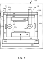
- a wafer alignment apparatus 100 includes a base 102 supporting an inverted U-shaped frame 104, first and second microscope sets 210a, 210b, a lower wafer support block 150 supporting a lower wafer 80 and an upper wafer support block 180 holding an upper wafer 90.
- Base 102 is made of a solid material and is supported on a table 106 via four vibration isolating legs 108a, 108b, 108c, 108d.
- base 102 is a rectangular shaped block made of granite material.
- base 102 may be made of metal or ceramic material and may have a honeycomb structure.
- the inverted U-shaped frame 104 includes left and right vertical legs 101, 103 respectively, and a beam 105 supported on the tops 113, 114 of the left and right legs 101, 103, respectively.
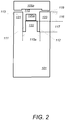
- Each of the leg tops 113, 114 includes two vertical slots 111, 112 extending from the top surface 119 of the leg toward the center of the leg, as shown in FIG.2 .
- Vertical slots 111, 112 divide the top of each leg 101, 103, respectively, into three separate block extensions 121, 122, 123, also shown in FIG. 2 .
- the ends 105a, 105b of beam 105 are fixedly attached to the outer two block extensions 121, 123 of each leg 101, 103, respectively.
- Gap 115 extends from the top surface 119 of the leg, has a height 116 less than the height 117 of the slots 111 and 112 and the same width as the distance 115a between the slots 111 and 112. Gap 115 is dimensioned to receive a support bar 120 extending from the top 113 of left leg 101 to the top 114 of right leg 103, as shown in FIG. 7 . Left and right ends 120a, 120b of support bar 120 are placed within the gaps 115 of the left and right legs 101, 103, respectively, and are fixedly attached to the inner blocks 122, as shown in FIG. 6 and FIG.
- Frame beam 105 supports two separate sets of microscope X-Y-Z stages 201a, 201b controlling the motion of the two microscope sets 210a, 210b, respectively.
- the upper wafer support block 180 is fixedly attached to support bar 120. The lack of contact between the ends 105a, 105b of the frame beam 105 and the ends 120a, 120b, of support bar 120 isolates the frame beam 105 from the support bar 120 and prevents the transfer of vibrations due to the microscope stage motion to the upper wafer support block 180 and therefore to the upper wafer 90.
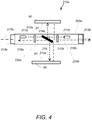
- each microscope set 210a, 210b includes two coaxially arranged microscopes 224a, 224b and 225a, 225b, placed within elongated tubes 202a, 202b, respectively.
- Each microscope 224a, 224b includes a light source 211a, 211b, a high performance objective lens 212a, 212b and a CCD camera 213a, 213b.
- a double-sided mirror 215 arranged at 45 degrees angle relative to the optical axis 217 is also included.
- Light 214a emitted from light source 211a is focused via the objective lens 212a and directed via the mirror 215 toward the lower wafer surface 81.
- Light 216a reflected by the lower wafer surface 81 is then directed by the mirror 215 and focused onto the CCD camera 213a.
- light 214b emitted from light source 211b is focused via the objective lens 212b and directed via the mirror 215 toward the upper wafer surface 91.
- Light 216b reflected by the upper wafer surface 91 is then directed by the mirror 215 and focused onto the CCD camera 213b.
- the surface images of the lower and upper wafer surfaces 81, 91 collected by the CCD cameras 213a, 213b are then used to align the wafer surfaces 81, 91 parallel to each other.
- light sources 211a, 211b are yellow Light Emitting Diodes (LED). In other examples, other visible or infrared light sources are used.
- Elongated tubes 202a, 202b are connected to inverted U-shape structures 204a, 204b that are carried by the microscope XYZ stages 201a, 201b, respectively, around the frame beam 105.
- Microscope stages 201a, 201b move the axes 217a, 217b of the microscopes in X, Y, Z directions.
- stages 201a, 201b are X-Y-Z-T stages and may also rotate the microscope axes around an axis perpendicular to them by an angle theta (T).
- the legs of the U-shape structures 204a, 204b are fixedly connected to plates 232a, 232b, 234a, 234b and plates 232a, 232b, 234a, 234b are connected to the ends of the elongated tubes 202a, 202b, via three kinematic couplings 233a, 233b, 233c, as shown in FIG. 8 .
- Mirrors 235a, 235b are also connected to plates 232a, 232b, respectively, separately from the elongated tubes, and are arranged below the elongated tubes 202a, 202b, so that the microscope axes 217a, 217b are parallel to the mirror planes 236a, 236b, respectively, shown in FIG.
- the apparatus includes left and right microscope calibration reference units 140a, 140b attached on the left and right frame legs 101, 103, respectively, shown in FIG. 1 and FIG. 7 .
- Each reference unit 140a, 140b includes fixed top and bottom reference marks K, K', L, L' located on fixed top and bottom plates 141a, 141b, 142a, 142b, respectively.
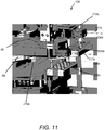
- the X-Y-Z and T coordinates of the two microscope optical axes 217a, 217b, and the angular position of the mirror planes 236a, 236b, shown in FIG. 11 are determined in reference to these fixed marks and are used as references for the wafer alignment process, as will be described below.
- upper wafer 90 is held via vacuum suction onto upper wafer block 180, so that surface 91 to be aligned parallel to the lower wafer surface 81 is facing down.
- Upper wafer block 180 includes an upper wafer plate 182 supporting the wafer 90 and a plate leveling system 184 for leveling upper wafer plate 182.
- the plate leveling system includes a spherical Wedge Error Compensating (WEC) mechanism that rotates and/or tilts the upper wafer plate 182 around a center point corresponding to the center of the wafer 90 without translation.
- WEC spherical Wedge Error Compensating
- Lower wafer 80 is held via vacuum suction onto lower wafer block 150, so that its surface 81 to be aligned parallel to the upper wafer surface 91 is facing up.
- Lower wafer block 150 includes a coarse X-Y-T air-bearing table 152 carrying an air bearing Z-stage 154, and a fine X-Y-T stage 155 is carried on top of the Z-stage.
- Fine X-Y-T stage 155 carries the lower wafer plate 156 upon which a fixture 300 carrying wafer 80 is positioned.
- coarse X-Y-T table 152 has a position range of ⁇ 3 millimeters and ⁇ 3 degrees
- fine X-Y-T stage has a position range of ⁇ 100 micrometers and ⁇ 1 millidegree and the Z-axis range is 60 millimeters.
- position sensors 157 Connected to the coarse X-Y-T stage 152 are three position sensors 157 that measure the X-Y-T - distance between the coarse stage 152 and fine stage 155 and provide feedback for the fine X-Y-T manipulation of the lower wafer surface plane 81.
- the position sensors 157 are capacitance gauges and are used for making high precision non-contact measurements of linear displacements.
- Upper and lower wafer plates 182, 156 are made of materials with CTE matching the CTE of the wafers.
- wafers 80, 90 are made of silicon and plates 182, 156 are made of silicon carbide. In other embodiments, separate sets of position sensors are placed on both the lower wafer plate and the upper wafer plate.
- a fixture 300 is used to transport the upper and lower wafers 90, 80 in and out of the alignment apparatus and to maintain the alignment of the two wafers for further processing, such as bonding of the wafers or further deposition steps.
- Fixture 300 includes an outer ring 310 supporting a lower wafer carrier chuck 315 and three clamp/spacer assemblies 320a, 320b, 320c, arranged at the periphery of ring 310.
- Each clamp/spacer assembly 320a includes a spacer 321a and a clamp 322a. The motion of clamp/spacer assemblies is very precise and repeatable both at room temperatures and at the high temperatures where the further wafer processing takes place.
- Wafer 80 is placed on top of lower wafer carrier chuck 315, the spacers 321a, 321b, 321c are inserted on top of the edges of the wafer surface 81, then the upper wafer 90 is placed on top of the spacers 321a, 321b, 321c, and then the upper wafer carrier chuck 316 is placed on top of the upper wafer 90 and the clamps 322a, 322b, 322c engage the upper wafer carrier chuck to clamp the two wafers together onto the fixture.
- the spacers 321a, 321b, 321c may be moved independent from each other from the clamping motion to bring the wafer surfaces 91, 81 in contact or to set a gap between them.
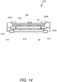
- the two clamped wafers may also be pinned together via a center pin 325, as shown in FIG. 14 .
- ring 310 is made of titanium and wafer carrier chucks 315, 316 are made of silicon carbide.
- the alignment process includes the following steps. First, microscope sets 210a, 210b are positioned in the reference units 140a, 140b and microscopes 224a, 224b and 225a, 225b are focused onto the fixed top and bottom reference marks K, K', L, L' located on the top and bottom plates 141a, 141b, 142a, 142b, respectively.
- a pattern recognition software is used to determine the X-Y coordinates of the fixed reference marks K, K', L, L' and their separation distance, as well as the angular positions theta (T) of the mirror planes 236a, 236b (reflecting the positions of microscope axes 217a, 217b) relative to the reference marks.
- Reference marks K, L and axis 217a define a reference plane 290a (shown in FIG. 20A ) for microscopes 224a, 224b and marks K', L' and axis 217b define a reference plane 290b (not shown) for microscopes 225a, 225b.
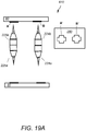
- the microscope sets 210a, 210b are inserted between the lower wafer 80 and upper wafer 90 and the X-Y-Z microscope stages 201a, 201b, are moved so that the images A', B' of the fiducial marks A, B, on the upper wafer surface 91 are brought into the field of view (FOV) 280 of the microscopes 224b, 225b looking up and the microscopes 224b, 225b are focused onto them, respectively, as shown in FIG. 19A .
- FOV field of view
- the microscope stages 201a, 201b are locked and then the lower wafer 80 is moved in the X-Y-T- and Z directions to bring the images C', D' of the lower wafer fiducial marks C, D, into the field of view 282 of the microscopes 224a, 224b looking down and to focus the microscopes 224a, 225a onto them, respectively, as shown in FIG. 19B .
- the positions of the fiducial marks A, B, C, D are determined by analyzing their images A', B', C', D' within the corresponding fields of view 280, 282 of microscopes 224b, 225b, 224a, 225a with the pattern recognition software Patmax ⁇ program available from Cognex Co, Natick Mass, and by taking into consideration the positions of the microscopes 224b, 225b, 224a, 225a relative to the reference planes 290a, 290b.
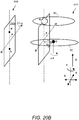
- any change in the mirror angles (and the upon them reflected optical axes 217a, 217b) is taken into consideration and the X-Y-T offsets ⁇ x, ⁇ y, ⁇ , shown in FIG.
- the lower wafer 80 (and carrier) is moved in the X-Y-T directions by the determined amount of the X-Y-T offsets ⁇ x, ⁇ y, ⁇ , to position the fiducial marks C, D of the lower wafer 80 in alignment with the fiducial marks A, B of the upper wafer 90, shown in FIG. 19C and FIG. 20C .
- the lower wafer 80 is moved up in the Z-direction while the X-Y-T position of wafer stage 155 is maintained by measuring its distance from the coarse stage 152 with the three co-planar position sensor 157 that are fixed on it and adjusting the position of wafer stage 155 so that the aligned lower wafer 80 position is maintained.
- the lower wafer 80 is moved up in the Z-direction until surface 81 contacts the surface 91 of the upper wafer 90.
- the aligned stack of wafers 80, 90 is clamped with clamps 322a, 322b, 322c onto the fixture 300 and is removed from the aligner for further processing, such as bonding of the two wafers.
- wafer 80 is moved up in the Z-direction until surface 81 contacts spacers 321a, 321b, 321c inserted between the two wafers.
- wafers 80 and 90 are clamped together while separated by a distance corresponding to the spacer thickness.
- the complete alignment sequence 600 is depicted in FIG. 18A - FIG. 18B and includes the following steps. Starting out, the microscopes are out of the space between the upper and lower blocks 180, 150 and the Z-axis of the X-Y-T-Z wafer stage 152 is down (601). Next, the fixture 300 with the upper and lower wafer chucks is loaded in the aligner and placed on the X-Y-T-Z wafer stage 152 (602). X-Y-T-Z wafer stage 152 is then moved up in the Z-direction and the upper chuck is handed over to the upper block 180 . X-Y-T-Z wafer stage 152 with the lower wafer chuck is then moved down (603).
- the upper wafer 90 is loaded in the aligner and transferred to the upper wafer chuck (604).
- the lower wafer is then loaded into the aligner and transferred onto the lower wafer chuck and the spacers are placed on top of the lower wafer surface (605).
- the z-axis of the lower wafer stage 152 is then moved up to bring the spacers in contact with the upper wafer 90 and to perform the Wedge Error Correction (WEC) on the upper wafer plate under force feedback control (606).
- WEC Wedge Error Correction
- the upper wafer plate position is locked and the z-axis is moved down and the spacers are removed (607).
- the microscopes are inserted in the fixed reference units and the upper microscopes are focused onto the fixed top marks and the lower microscopes are focused onto the fixed bottom marks (608).
- the fixed mark images are analyzed with an image pattern recognition software and their position, the distance from each other and the mirror angular positions (i.e., axes of the microscopes) are determined (609). These measurements define the reference point (i.e., center of coordinate system) for the further measurements.
- the microscopes are inserted between the upper and lower wafer and the upper directed microscopes are focused onto the upper wafer marks.
- the microscope positions are then locked (610).
- the lower X-Y-T-Z wafer stage 152 is then moved to focus the lower directed microscopes onto the lower wafer marks and the stage position is locked (611).
- the images of the upper and lower marks are analyzed with the image pattern recognition software and their position relative to the fixed mark positions and the X-Y-T offsets between them are determined and the mirror angular positions (i.e., axes of the microscopes) are also measured (612).
- the lower wafer fine stage is then moved by the X-Y-T offset amount and by the amount determined by the global calibration, as is described below (613).
- the microscopes are moved out of the space between the upper and lower wafer (614) and the lower wafer stage is moved up in the z-direction while the X-Y-T alignment of the fine wafer stage is maintained with the help of the position sensors (615).
- the lower wafer 80 is brought into contact with the upper wafer 90 and the stack is clamped together (616) in the fixture 300. Finally, the aligned wafer set and fixture are removed from the aligner and placed into another process chamber (617) for further processing such as bonding or deposition.
- the aligner system 100 is calibrated with a global calibration device 400 shown in FIG. 14- FIG.17 .
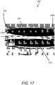
- Global calibration device 400 includes a lower plate 415, an upper plate 425 and a clear transparent wafer 430 (shown in FIG. 17 ) arranged between them.
- Lower plate 415 includes concentric vacuum grooves 418 and fiducial marks 416a, 416b.
- Upper plate 425 includes vacuum grooves 419 and transparent wafer 430 includes fiducial marks 432a, 432b.
- Lower plate 415, transparent wafer 430 and upper plate 425 are placed in fixture 300 and are placed in the aligner apparatus 100.
- the above described alignment process 600 is performed to bring the fiducial marks 432a, 432b of the transparent wafer 430 in alignment with the fiducial marks 416a, 416b of the lower plate 415.
- the transparent wafer 430 is placed in contact with the lower plate and the overlap of the transparent wafer marks 432a, 432b with the lower plate marks 416a, 416b is observed with the down focusing microscopes 225a, 224a. Any X-Y-T offsets between these marks are measured, as well as the mirror angular positions and are used for the global calibration correction.
- the entire aligner 100 may be enclosed in a controlled atmosphere, temperature and pressure chamber 70, as shown in FIG. 1 .
- the microscope stages 201a, 201b may be X-Y-Z-T stages.
Landscapes
- Container, Conveyance, Adherence, Positioning, Of Wafer (AREA)
Description
- The present invention relates to an apparatus and a method for semiconductor alignment, and more particularly to an interwafer wafer-to-wafer alignment that provides nanometer range alignment accuracy.
- Alignment of semiconductor wafers is usually achieved by utilizing mechanical or optical fiducial marks, such as notches at the edges of wafers, pins, e-beam etchings, or holographic images, among others. Mechanical alignment marks provide millimeter range alignment accuracy, while optical marks provide micron to submicron alignment accuracy.
- In several semiconductor processes, such as 3-D integration, bonding and mask alignment, among others, submicron to nanometer alignment accuracy is desirable.
WO 2005/071735 A1 shows an apparatus for bonding a device to a substrate having a movable device for identifying alignment marks for aligning the device to the substrate. - A wafer-to-wafer alignment apparatus and method according to this invention utilize microscopes that are inserted between two wafers to be aligned parallel to each other. This "interwafer" alignment method can be used for any type of wafer material, transparent or not transparent, uses visible light and does not require fiducial marks at the back of the wafers. The alignment accuracy is of the order of a few hundred nanometers.
- In general, in one aspect, the invention features an apparatus for aligning semiconductor wafers according to claim 1.
- Implementations of this aspect of the invention may include one or more of the following features. The positioning equipment are vibrationally and mechanically isolated from the alignment equipment. The apparatus may further include an inverted U-shaped frame and a vibration isolated base. The inverted U-shaped frame is supported on a top surface of the base. The inverted U-shaped frame includes left and right vertical columns and a horizontal beam comprising left and right ends. Each of the column tops comprises two parallel vertical slots extending from the column top surface toward the column center and the two vertical slots are separated by a center block. The center block extends from the bottom of the slots toward the column top and has a height less than the height of the vertical slots thereby forming a gap between the two vertical slots near the column top surface. The left and right ends of the horizontal beam are supported upon the center blocks of the left and right vertical columns, respectively. The apparatus may further include an XYZ stage supporting the movable alignment device and the XYZ stage is configured to slide along the horizontal beam and be supported by the horizontal beam. The movable alignment device includes an optical microscope assembly including an elongated tube and first and second optical microscopes arranged coaxially within the elongated tube along a first axis. The first and second optical microscopes are configured to obtain first and second images of the first and second structures, respectively. The first and second images of the first and second structures are used to determine coordinates of the first and second structures relative to fixed top and bottom reference marks and to guide the positioning equipment for aligning the first surfaces of the first and second semiconductor wafers parallel to each other. The calibration reference unit may be attached to one of the vertical columns. The optical microscope assembly may further include a mirror plane arranged so that the first axis is parallel to the mirror plane. The apparatus may further include pattern recognition software used to analyze the first and second images of the first and second structures, respectively, and to determine their coordinates relative to the fixed top and bottom reference marks. The positioning equipment includes a lower support block and an upper supporting block. The lower supporting block includes a lower wafer plate supporting the first semiconductor wafer and the upper supporting block includes an upper wafer plate supporting the second semiconductor wafer and a plate leveling system for leveling the upper wafer plate. The plate leveling system includes a spherical wedge error compensation mechanism that rotates and/or tilts the upper wafer plate around a center point corresponding to the center of the second semiconductor wafer without translation. The lower support block includes a coarse X-Y-T stage, an air bearing Z-stage carried by the coarse X-Y-T stage and a fine X-Y-T stage carried on top of the Z-stage, and wherein the X-Y-T fine stage carries the lower wafer plate. The X-Y-T coarse stage further includes one or more position sensors for measuring the X-Y-T distance between the coarse X-Y-T stage and the fine X-Y-T stage. The position sensors may be capacitance gauges. The upper and lower wafer plates comprise materials having a CTE matching the semiconductor wafer CTE. The apparatus may further include a fixture for transporting the first and second semiconductor wafers. The fixture includes an outer ring supporting a lower wafer carrier chuck and three or more clamp/spacer assemblies arranged at the periphery of the outer ring. Each of the clamp/spacer assemblies includes a clamp and a spacer. The clamp and the spacer are configured to be moved independent from each other and from the motion of clamps or spacers of the other assemblies and the motion is precise and repeatable both at room and high temperatures. The fixture further may further include a center pin for pinning together the centers of the first and second semiconductor wafers. The first semiconductor wafer is placed upon the lower wafer carrier chuck, the spacers are inserted on top of the edge of the first semiconductor wafer surface and then the second semiconductor wafer is placed on top of the spacers and then the first and second semiconductor wafers are clamped together via the clamps.
- In general, in another aspect, the invention may feature an apparatus for aligning semiconductor wafers including equipment for positioning a first surface of a first semiconductor wafer directly opposite to a first surface of a second semiconductor wafer and equipment for aligning a first structure on the first semiconductor wafer with a second structure on the first surface of the second semiconductor wafer. The aligning equipment includes at least one movable alignment device configured to be moved during alignment. The positioning equipment are vibrationally and mechanically isolated from the alignment device motion.
- In general, in another aspect, the invention features a method for aligning semiconductor wafers according to claim 18.
- Implementations of this aspect of the invention may include one or more of the following features. The positioning step is vibrationally and mechanically isolated from the inserting of the movable alignment device between the first surface of the first semiconductor wafer and the first surface of the second semiconductor wafer. The movable alignment device includes an optical microscope assembly including an elongated tube and first and second optical microscopes arranged coaxially within the elongated tube along a first axis. The first and second optical microscopes are configured to obtain first and second images of the first and second structures, respectively. The first and second images of the first and second structures are used to determine coordinates of the first and second structures relative to fixed top and bottom reference marks and to guide the positioning equipment for aligning the first surfaces of the first and second semiconductor wafers parallel to each other. The apparatus further includes a microscope calibration reference unit including fixed top and bottom reference marks. The calibration reference unit may be attached to one of the vertical columns. The optical microscope assembly may further include a mirror plane arranged so that the first axis is parallel to the mirror plane. The method may further include providing pattern recognition software for analyzing the first and second images of the first and second structures, respectively, and determining their coordinates relative to the fixed top and bottom reference marks. The positioning step may include providing a lower support block comprising a lower wafer plate and placing the first semiconductor wafer upon the lower wafer plate and then providing an upper supporting block comprising an upper wafer plate for supporting the second semiconductor wafer and a plate leveling system for leveling the upper wafer plate. The plate leveling system may include a spherical wedge error compensation mechanism that rotates and/or tilts the upper wafer plate around a center point corresponding to the center of the second semiconductor wafer without translation. The lower support block includes a coarse X-Y-T stage, an air bearing Z-stage carried by the coarse X-Y-T stage and a fine X-Y-T stage carried on top of the Z-stage, and wherein the X-Y-T fine stage carries the lower wafer plate. The X-Y-T coarse stage further includes one or more position sensors for measuring the X-Y-T distance between the coarse X-Y-T stage and the fine X-Y-T stage. The apparatus may further include a fixture for transporting the first and second semiconductor wafers. The fixture includes an outer ring supporting a lower wafer carrier chuck and three or more clamp/spacer assemblies arranged at the periphery of the outer ring. Each of the clamp/spacer assemblies includes a clamp and a spacer. The clamp and the spacer are configured to be moved independent from each other and from the motion of clamps or spacers of the other assemblies and the motion is precise and repeatable both at room and high temperatures. The fixture further may further include a center pin for pinning together the centers of the first and second semiconductor wafers. The aligning of the first structure with the second structure includes the following steps. First, placing the first semiconductor wafer upon the lower support block with its first surface facing up. Next, supporting the second semiconductor wafer by the upper wafer plate with its first surface facing down. Next, inserting the optical microscope assembly into the fixed reference unit and focusing the first and second optical microscopes onto the fixed bottom and top reference marks, respectively. Next, using the pattern recognition software to determine position and distance of the fixed top and bottom reference marks and the mirror plane angular position. Next, inserting the optical microscope assembly between the first surfaces of the first and second semiconductor wafers, and focusing the second optical microscope onto the second structure of the second semiconductor wafer and then locking the optical microscope assembly position. Next, moving the coarse X-Y-T stage and Z-stage to focus the first microscope onto the first structure of the first semiconductor wafer and locking coarse X-Y-T and Z stages. Next, using the pattern recognition software to determine position coordinates of the first and second structures and determine their offsets. Finally, moving fine X-Y-T stage by the amount of the determined offsets and an amount determined by a global calibration method, thereby bringing the first and second structures in alignment with each other. The alignment of the first and second structures may further include the following. Moving the optical microscope assembly out from in between the first surfaces of the first and second semiconductor wafers and then moving the Z-stage up while maintaining the fine X-Y-T stage alignment with feedback from the position sensors. Next, bringing the first surface of the first semiconductor wafer in contact with the first surface of the second semiconductor wafer, then clamping the first and second semiconductor wafers together and then unloading the aligned first and second semiconductor wafers. After supporting the second semiconductor wafer by the upper wafer plate the method may further include moving the Z-stage up to bring the spacers on top of the first semiconductor wafer first surface in contact with the second semiconductor first surface. Next, performing wedge error compensation of the second semiconductor wafer under force feedback control and locking the wedge position and then moving the first semiconductor wafer down and removing the spacers.
- The details of one or more embodiments of the invention are set forth in the accompanying drawings and description below. Other features, objects and advantages of the invention will be apparent from the following description of the preferred embodiments, the drawings and from the claims.
- Referring to the figures, wherein like numerals represent like parts throughout the several views:
-
FIG. 1 is a schematic diagram of an aligner system according to this invention; -
FIG. 2 is a detailed side view of area P ofFIG.1 ; -
FIG. 3 is a schematic side view of the aligner system ofFIG.1 ; -
FIG. 4 is a schematic diagram of the microscope system ofFIG. 1 ; -
FIG. 5 is a perspective view of the aligner apparatus according tot his invention; -
FIG. 6 is a perspective side view of the aligner apparatus ofFIG. 3 ; -
FIG. 7 is a front cross-sectional view of the aligner apparatus ofFIG. 3 ; -
FIG. 8 is a perspective top view of the microscope system ofFIG. 3 ; -
FIG. 9 is a perspective side view of the microscope system ofFIG. 8 ; -
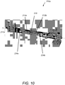
FIG. 10 is a cross-sectional side view of the microscope system ofFIG. 8 ; -
FIG. 11 is detailed view of the two microscope systems within the aligner ofFIG. 8 ; -
FIG. 12 is a top view of the wafer fixture tool; -
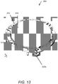
FIG. 13 is a top view of the wafer fixture tool loaded with the top and lower plates; -
FIG. 14 is a schematic cross-sectional view of the wafer fixture tool loaded with the top and lower plates and wafers in the clamped position; -
FIG. 15 is a top view of the lower plate of the global calibration device; -
FIG. 16 is a side view of the top and lower plates of the global calibration device; -
FIG. 17 is a side view of the top and lower plates and transparent wafer of the global calibration device ; -
FIG. 18A- FIG.18B is a flow diagram of the alignment process; -
FIG. 19A is a schematic diagram ofstep 610 of the alignment process ofFIG. 18B ; -
FIG. 19B is a schematic diagram ofstep 611 of the alignment process ofFIG. 18B ; -
FIG. 19C is a schematic diagram ofstep 613 of the alignment process ofFIG. 18B ; -
FIG. 20A is a schematic diagram of steps, 608 and 611 of the alignment process ofFIG. 18A - FIG. 18B ; -
FIG. 20B is a schematic diagram of steps, 608 and 612 of the alignment process ofFIG. 18A - FIG. 18B ; and -
FIG. 20C is a schematic diagram of steps, 608 and 613 of the alignment process ofFIG. 18A - FIG. 18B . - Referring to
FIG.1-FIG.5 awafer alignment apparatus 100, includes a base 102 supporting an invertedU-shaped frame 104, first and second microscope sets 210a, 210b, a lowerwafer support block 150 supporting alower wafer 80 and an upperwafer support block 180 holding anupper wafer 90.Base 102 is made of a solid material and is supported on a table 106 via fourvibration isolating legs base 102 is a rectangular shaped block made of granite material. In other examples,base 102 may be made of metal or ceramic material and may have a honeycomb structure. The invertedU-shaped frame 104 includes left and rightvertical legs beam 105 supported on the tops 113, 114 of the left andright legs vertical slots top surface 119 of the leg toward the center of the leg, as shown inFIG.2 .Vertical slots leg separate block extensions FIG. 2 . Theends beam 105 are fixedly attached to the outer twoblock extensions leg Vertical slots distance 115a and agap 115 is formed between them, as shown inFIG. 2 .Gap 115 extends from thetop surface 119 of the leg, has aheight 116 less than theheight 117 of theslots distance 115a between theslots Gap 115 is dimensioned to receive asupport bar 120 extending from the top 113 ofleft leg 101 to the top 114 ofright leg 103, as shown inFIG. 7 . Left and right ends 120a, 120b ofsupport bar 120 are placed within thegaps 115 of the left andright legs inner blocks 122, as shown inFIG. 6 andFIG. 2 . In this type of arrangement there is no contact between theends frame beam 105 and theends support bar 120.Frame beam 105 supports two separate sets of microscopeX-Y-Z stages microscope sets wafer support block 180 is fixedly attached to supportbar 120. The lack of contact between theends frame beam 105 and theends support bar 120 isolates theframe beam 105 from thesupport bar 120 and prevents the transfer of vibrations due to the microscope stage motion to the upperwafer support block 180 and therefore to theupper wafer 90. - Referring to
FIG. 3 and4 , each microscope set 210a, 210b, includes two coaxially arrangedmicroscopes elongated tubes microscope light source performance objective lens CCD camera sided mirror 215 arranged at 45 degrees angle relative to the optical axis 217 is also included.Light 214a emitted fromlight source 211a is focused via theobjective lens 212a and directed via themirror 215 toward thelower wafer surface 81.Light 216a reflected by thelower wafer surface 81 is then directed by themirror 215 and focused onto theCCD camera 213a. Similarly, light 214b emitted fromlight source 211b is focused via theobjective lens 212b and directed via themirror 215 toward theupper wafer surface 91. Light 216b reflected by theupper wafer surface 91 is then directed by themirror 215 and focused onto theCCD camera 213b. The surface images of the lower and upper wafer surfaces 81, 91 collected by theCCD cameras light sources -
Elongated tubes U-shape structures microscope XYZ stages frame beam 105.Microscope stages axes embodiments stages U-shape structures plates plates elongated tubes kinematic couplings FIG. 8 .Mirrors plates 232a, 232b, respectively, separately from the elongated tubes, and are arranged below theelongated tubes microscope axes mirror planes FIG. 11 . Furthermore, the apparatus includes left and right microscopecalibration reference units right frame legs FIG. 1 andFIG. 7 . Eachreference unit bottom plates optical axes mirror planes FIG. 11 , are determined in reference to these fixed marks and are used as references for the wafer alignment process, as will be described below. - Referring to
FIG. 7 ,upper wafer 90 is held via vacuum suction ontoupper wafer block 180, so thatsurface 91 to be aligned parallel to thelower wafer surface 81 is facing down.Upper wafer block 180 includes anupper wafer plate 182 supporting thewafer 90 and aplate leveling system 184 for levelingupper wafer plate 182. The plate leveling system includes a spherical Wedge Error Compensating (WEC) mechanism that rotates and/or tilts theupper wafer plate 182 around a center point corresponding to the center of thewafer 90 without translation.Lower wafer 80 is held via vacuum suction ontolower wafer block 150, so that itssurface 81 to be aligned parallel to theupper wafer surface 91 is facing up.Lower wafer block 150 includes a coarse X-Y-T air-bearing table 152 carrying an air bearing Z-stage 154, and a fineX-Y-T stage 155 is carried on top of the Z-stage. FineX-Y-T stage 155 carries thelower wafer plate 156 upon which afixture 300 carryingwafer 80 is positioned. In one example, coarse X-Y-T table 152 has a position range of ± 3 millimeters and ±3 degrees, while fine X-Y-T stage has a position range of ± 100 micrometers and ±1 millidegree and the Z-axis range is 60 millimeters. Connected to the coarseX-Y-T stage 152 are threeposition sensors 157 that measure the X-Y-T - distance between thecoarse stage 152 andfine stage 155 and provide feedback for the fine X-Y-T manipulation of the lowerwafer surface plane 81. In one example, theposition sensors 157 are capacitance gauges and are used for making high precision non-contact measurements of linear displacements. Upper andlower wafer plates wafers plates - Referring to
FIG. 12 , afixture 300 is used to transport the upper andlower wafers Fixture 300 includes anouter ring 310 supporting a lowerwafer carrier chuck 315 and three clamp/spacer assemblies ring 310. Each clamp/spacer assembly 320a includes aspacer 321a and aclamp 322a. The motion of clamp/spacer assemblies is very precise and repeatable both at room temperatures and at the high temperatures where the further wafer processing takes place.Wafer 80 is placed on top of lowerwafer carrier chuck 315, thespacers wafer surface 81, then theupper wafer 90 is placed on top of the spacers 321a, 321b, 321c, and then the upperwafer carrier chuck 316 is placed on top of theupper wafer 90 and theclamps spacers center pin 325, as shown inFIG. 14 . In oneexample ring 310 is made of titanium and wafer carrier chucks 315, 316 are made of silicon carbide. - Referring to
FIG. 18A-FIG.20C , the alignment process includes the following steps. First, microscope sets 210a, 210b are positioned in thereference units microscopes bottom plates mirror planes microscope axes axis 217a define areference plane 290a (shown inFIG. 20A ) formicroscopes axis 217b define a reference plane 290b (not shown) formicroscopes lower wafer 80 andupper wafer 90 and theX-Y-Z microscope stages upper wafer surface 91 are brought into the field of view (FOV) 280 of themicroscopes microscopes FIG. 19A . The microscope stages 201a, 201b are locked and then thelower wafer 80 is moved in the X-Y-T- and Z directions to bring the images C', D' of the lower wafer fiducial marks C, D, into the field ofview 282 of themicroscopes microscopes FIG. 19B . Next, the positions of the fiducial marks A, B, C, D are determined by analyzing their images A', B', C', D' within the corresponding fields ofview microscopes microscopes reference planes 290a, 290b. In addition to the microscope positions any change in the mirror angles (and the upon them reflectedoptical axes FIG. 20B , between the upper fiducial marks A, B and lower fiducial marks C, D are determined. Next, the lower wafer 80 (and carrier) is moved in the X-Y-T directions by the determined amount of the X-Y-T offsets Δx, Δy, Δθ, to position the fiducial marks C, D of thelower wafer 80 in alignment with the fiducial marks A, B of theupper wafer 90, shown inFIG. 19C andFIG. 20C . This results with thelower wafer 80 being in alignment with theupper wafer 90 while they are separated by adistance 294. Next, thelower wafer 80 is moved up in the Z-direction while the X-Y-T position ofwafer stage 155 is maintained by measuring its distance from thecoarse stage 152 with the threeco-planar position sensor 157 that are fixed on it and adjusting the position ofwafer stage 155 so that the alignedlower wafer 80 position is maintained. Thelower wafer 80 is moved up in the Z-direction untilsurface 81 contacts thesurface 91 of theupper wafer 90. The aligned stack ofwafers clamps fixture 300 and is removed from the aligner for further processing, such as bonding of the two wafers. In other embodiments,wafer 80 is moved up in the Z-direction untilsurface 81 contacts spacers 321a, 321b, 321c inserted between the two wafers. In thisconfiguration wafers - The
complete alignment sequence 600 is depicted inFIG. 18A - FIG. 18B and includes the following steps. Starting out, the microscopes are out of the space between the upper andlower blocks X-Y-T-Z wafer stage 152 is down (601). Next, thefixture 300 with the upper and lower wafer chucks is loaded in the aligner and placed on the X-Y-T-Z wafer stage 152 (602).X-Y-T-Z wafer stage 152 is then moved up in the Z-direction and the upper chuck is handed over to theupper block 180 .X-Y-T-Z wafer stage 152 with the lower wafer chuck is then moved down (603). Next, theupper wafer 90 is loaded in the aligner and transferred to the upper wafer chuck (604). The lower wafer is then loaded into the aligner and transferred onto the lower wafer chuck and the spacers are placed on top of the lower wafer surface (605). The z-axis of thelower wafer stage 152 is then moved up to bring the spacers in contact with theupper wafer 90 and to perform the Wedge Error Correction (WEC) on the upper wafer plate under force feedback control (606). The upper wafer plate position is locked and the z-axis is moved down and the spacers are removed (607). Next the microscopes are inserted in the fixed reference units and the upper microscopes are focused onto the fixed top marks and the lower microscopes are focused onto the fixed bottom marks (608). The fixed mark images are analyzed with an image pattern recognition software and their position, the distance from each other and the mirror angular positions (i.e., axes of the microscopes) are determined (609). These measurements define the reference point (i.e., center of coordinate system) for the further measurements. Next, the microscopes are inserted between the upper and lower wafer and the upper directed microscopes are focused onto the upper wafer marks. The microscope positions are then locked (610). The lowerX-Y-T-Z wafer stage 152 is then moved to focus the lower directed microscopes onto the lower wafer marks and the stage position is locked (611). The images of the upper and lower marks are analyzed with the image pattern recognition software and their position relative to the fixed mark positions and the X-Y-T offsets between them are determined and the mirror angular positions (i.e., axes of the microscopes) are also measured (612). The lower wafer fine stage is then moved by the X-Y-T offset amount and by the amount determined by the global calibration, as is described below (613). Next, the microscopes are moved out of the space between the upper and lower wafer (614) and the lower wafer stage is moved up in the z-direction while the X-Y-T alignment of the fine wafer stage is maintained with the help of the position sensors (615). Thelower wafer 80 is brought into contact with theupper wafer 90 and the stack is clamped together (616) in thefixture 300. Finally, the aligned wafer set and fixture are removed from the aligner and placed into another process chamber (617) for further processing such as bonding or deposition. - The
aligner system 100 is calibrated with aglobal calibration device 400 shown inFIG. 14- FIG.17 .Global calibration device 400 includes alower plate 415, anupper plate 425 and a clear transparent wafer 430 (shown inFIG. 17 ) arranged between them.Lower plate 415 includesconcentric vacuum grooves 418 andfiducial marks Upper plate 425 includesvacuum grooves 419 andtransparent wafer 430 includesfiducial marks Lower plate 415,transparent wafer 430 andupper plate 425 are placed infixture 300 and are placed in thealigner apparatus 100. The above describedalignment process 600 is performed to bring thefiducial marks transparent wafer 430 in alignment with thefiducial marks lower plate 415. Next, thetransparent wafer 430 is placed in contact with the lower plate and the overlap of thetransparent wafer marks lower plate marks down focusing microscopes - In some embodiments, the
entire aligner 100 may be enclosed in a controlled atmosphere, temperature andpressure chamber 70, as shown inFIG. 1 . The microscope stages 201a, 201b may be X-Y-Z-T stages.
Claims (18)
- An apparatus for aligning semiconductor wafers (80, 90) comprising:equipment for positioning a first surface (81) of a first semiconductor wafer (80) directly opposite to a first surface (91) of a second semiconductor wafer (90);equipment for aligning a first structure on said first semiconductor wafer (80) with a second structure on said first surface (91) of said second semiconductor wafer (90) and wherein said aligning equipment comprises at least one movable alignment device configured to be moved during alignment and to be inserted between said first surface (81) of said first semiconductor wafer (80) and said first surface (91) of said second semiconductor wafer (90); andwherein said positioning equipment comprises:a lower support block (150) comprising a lower wafer plate (156) supporting said first semiconductor wafer (80); andan upper support block (180) comprising an upper wafer plate (182) supporting said second semiconductor wafer (90) and a plate leveling system (184) for leveling said upper wafer plate (182);wherein said movable alignment device comprises an optical microscope assembly (210a, 210b);characterized in that said alignment equipment further comprises a microscope calibration reference unit (140a, 140b) including fixed top and bottom reference marks (K, K', L, L').
- The apparatus of claim 1 wherein said positioning equipment are vibrationally and mechanically isolated from said alignment equipment.
- The apparatus of claim 2 further comprising an inverted U-shaped frame (104) and a vibration isolated base (102) and wherein said inverted U-shaped frame (104) is supported on a top surface of said base (102).
- The apparatus of claim 3 wherein said inverted U-shaped (104) frame comprises:left and right vertical columns (101, 103);a horizontal beam (105) comprising left and right ends (105a, 105b);wherein each of said column tops (113, 114) comprises two parallel vertical slots (111, 112) extending from said column top surface (119) toward said column center and wherein said two vertical slots (111, 112) are separated by a center block (122) and wherein said center block (122) extends from the bottom of said slots toward said column top (113, 114) and has a height less than the height (117) of said vertical slots (111, 112) thereby forming a gap (115) between said two vertical slots (111, 112) near said column top surface (119); andwherein said left and right ends (105a, 105b) of said horizontal beam (105) are supported upon said center blocks (122) of said left and right vertical columns (101, 103), respectively.
- The apparatus of claim 4 further comprising a XYZ-stage (201a, 201b) supporting said movable alignment device and wherein said XYZ-stage (201a, 201b) is configured to slide along said horizontal beam (105) and be supported by said horizontal beam (105).
- The apparatus of claim 1 wherein said optical microscope assembly (210a, 210b) comprises:an elongated tube (202a, 202b);first and second optical microscopes (224a, 224b, 225a, 225b) arranged coaxially within said elongated tube (202a, 202b) along a first axis (217a, 217b);wherein said first and second optical microscopes (224a, 224b, 225a, 225b) are configured to obtain first and second images (A', B', C', D') of said first and second structures (A, B, C, D), respectively; andwherein the apparatus is adapted to execute the following steps:
use said first and second images (A', B', C', D') of said first and second structures (A, B, C, D) to determine coordinates of said first and second structures (A, B, C, D) relative to fixed top and bottom reference marks (K, K', L, L') and to guide said positioning equipment for aligning said first surfaces (81, 91) of said first and second semiconductor wafers (80, 90) parallel to each other. - The apparatus of claim 6 wherein said calibration reference unit (140a, 140b) is attached to one of said vertical columns (101, 103).
- The apparatus of claim 7 wherein said optical microscope assembly (210a, 210b) further comprises a mirror plane (236a, 236b) arranged so that said first axis (217a, 217b) is parallel to said mirror plane (236a, 236b).
- The apparatus of claim 8 further comprising a pattern recognition software used to analyze said first and second images (A', B', C', D') of said first and second structures (A, B, C, D), respectively, and to determine their coordinates relative to said fixed top and bottom reference marks (K, K', L, L').
- The apparatus of any one of claims 1 to 9 wherein said plate leveling system (184) comprises a spherical wedge error compensation mechanism that rotates and/or tilts said upper wafer plate (182) around a center point corresponding to the center of said second semiconductor wafer (90) without translation.
- The apparatus of claim 10 wherein said lower support block (150) comprises a coarse X-Y-Θ stage (152), an air bearing Z-stage (154) carried by said coarse X-Y-Θ stage (152) and a fine X-Y-Θ stage (155) carried on top of said Z-stage (154), and wherein said X-Y-Θ fine stage (155) carries said lower wafer plate (156).
- The apparatus of claim 11 wherein said X-Y-Θ coarse stage (152) further comprises one or more position sensors (157) for measuring the X-Y-Θ distance between said coarse X-Y-Θ stage (152) and said fine X-Y-Θ stage (155).
- The apparatus of claim 12 wherein said position sensors (157) comprise capacitance gauges.
- The apparatus of claim 13 wherein said upper and lower wafer plates (182, 156) comprise materials having a coefficient of thermal expansion, CTE, matching the semiconductor wafer CTE.
- The apparatus of claim 1 further comprising a fixture (300) for transporting said first and second semiconductor wafers (80, 90), said fixture (300) comprising an outer ring (310) supporting a lower wafer carrier chuck (315) and three or more clamp/spacer assemblies (320a, 320b, 320c) arranged at the periphery of said outer ring (310).
- The apparatus of claim 15 wherein each of said clamp/spacer assemblies (320a, 320b, 320c) comprise a clamp (322a, 322b, 322c) and a spacer (321a, 321b, 321c) and wherein said clamp (322a, 322b, 322c) and said spacer (321a, 321b, 321c) are configured to be moved independent from each other and from the motion of clamps (322a, 322b, 322c) or spacers (321a, 321b, 321c) of the other assemblies (320a, 320b, 320c).
- The apparatus of claim 16 wherein said fixture (300) further comprises a center pin (325) for pinning together the centers of said first and second semiconductor wafers (80, 90).
- A method for aligning semiconductor wafers (80, 90) using the apparatus of any one of the preceding claims comprising:positioning a first surface (81) of a first semiconductor wafer (80) directly opposite to a first surface (91) of a second semiconductor wafer (90); andproviding alignment equipment comprising at least one movable alignment device; andaligning a first structure (C, D) on said first semiconductor wafer (80) with a second structure (A, B) on said first surface (91) of said second semiconductor wafer (90) by inserting said movable alignment device between said first surface (81) of said first semiconductor wafer (80) and said first surface (91) of said second semiconductor wafer (90).
Applications Claiming Priority (3)
| Application Number | Priority Date | Filing Date | Title |
|---|---|---|---|
| US4162908P | 2008-04-02 | 2008-04-02 | |
| US12/416,779 US8139219B2 (en) | 2008-04-02 | 2009-04-01 | Apparatus and method for semiconductor wafer alignment |
| PCT/US2009/039238 WO2009146091A1 (en) | 2008-04-02 | 2009-04-02 | Apparatus and method for semiconductor wafer alignment |
Publications (3)
| Publication Number | Publication Date |
|---|---|
| EP2279521A1 EP2279521A1 (en) | 2011-02-02 |
| EP2279521A4 EP2279521A4 (en) | 2013-01-02 |
| EP2279521B1 true EP2279521B1 (en) | 2020-07-08 |
Family
ID=41132962
Family Applications (1)
| Application Number | Title | Priority Date | Filing Date |
|---|---|---|---|
| EP09755453.9A Active EP2279521B1 (en) | 2008-04-02 | 2009-04-02 | Apparatus and method for semiconductor wafer alignment |
Country Status (5)
| Country | Link |
|---|---|
| US (1) | US8139219B2 (en) |
| EP (1) | EP2279521B1 (en) |
| JP (1) | JP5586580B2 (en) |
| KR (1) | KR101640612B1 (en) |
| WO (1) | WO2009146091A1 (en) |
Families Citing this family (40)
| Publication number | Priority date | Publication date | Assignee | Title |
|---|---|---|---|---|
| TWI478272B (en) * | 2007-08-15 | 2015-03-21 | 尼康股份有限公司 | A positioning device, a bonding device, a laminated substrate manufacturing device, an exposure device, and a positioning method |
| EP2299472B1 (en) * | 2009-09-22 | 2020-07-08 | EV Group E. Thallner GmbH | Device for aligning two substrates |
| DE102010007970A1 (en) * | 2010-02-15 | 2011-08-18 | Suss MicroTec Lithography GmbH, 85748 | Method and device for active wedge error compensation between two objects which can be positioned substantially parallel to one another |
| NL2007215A (en) * | 2010-09-08 | 2012-03-12 | Asml Netherlands Bv | Lithographic apparatus, device manufacturing method, and method of applying a pattern to a substrate. |
| EP3528276A3 (en) | 2011-05-13 | 2019-09-04 | Fibics Incorporated | Microscopy imaging method |
| US9123754B2 (en) | 2011-10-06 | 2015-09-01 | Taiwan Semiconductor Manufacturing Company, Ltd. | Bonding alignment tool and method |
| KR20130102209A (en) * | 2012-03-07 | 2013-09-17 | 삼성전자주식회사 | Apparatus and method for wafer alignment |
| US9083863B2 (en) | 2012-04-20 | 2015-07-14 | Hewlett-Packard Development Company, L.P. | Alignment system for a digital image capture device |
| JP5993625B2 (en) * | 2012-06-15 | 2016-09-14 | 株式会社Screenホールディングス | Substrate reversing apparatus and substrate processing apparatus |
| KR101332082B1 (en) * | 2012-06-18 | 2013-11-22 | 삼성전기주식회사 | Apparatus for manufacturing camera module |
| CN104703762A (en) * | 2012-10-05 | 2015-06-10 | 贝克曼考尔特公司 | System and method for camera-based auto-alignment |
| EP2934821A1 (en) | 2012-12-21 | 2015-10-28 | Beckman Coulter, Inc. | System and method for laser-based auto-alignment |
| WO2014105989A1 (en) | 2012-12-31 | 2014-07-03 | Flir Systems, Inc. | Wafer level packaging of microbolometer vacuum package assemblies |
| EP2752870A1 (en) * | 2013-01-04 | 2014-07-09 | Süss Microtec Lithography GmbH | Chuck, in particular for use in a mask aligner |
| US20160042987A1 (en) * | 2013-03-15 | 2016-02-11 | Rudolph Technologies, Inc. | Flexible handling system for semiconductor substrates |
| SG2014014054A (en) * | 2013-06-17 | 2014-10-30 | Ev Group E Thallner Gmbh | Device and Method for Alignment of substrates |
| US9646860B2 (en) * | 2013-08-09 | 2017-05-09 | Taiwan Semiconductor Manufacturing Company, Ltd. | Alignment systems and wafer bonding systems and methods |
| US9299598B2 (en) | 2013-12-23 | 2016-03-29 | Lam Research Corp. | Robot with integrated aligner |
| CN105023869B (en) * | 2014-04-25 | 2018-03-02 | 上海微电子装备(集团)股份有限公司 | Semi-automatic alignment machine |
| US9640418B2 (en) * | 2015-05-15 | 2017-05-02 | Suss Microtec Lithography Gmbh | Apparatus, system, and method for handling aligned wafer pairs |
| US11183401B2 (en) | 2015-05-15 | 2021-11-23 | Suss Microtec Lithography Gmbh | System and related techniques for handling aligned substrate pairs |
| US9405287B1 (en) | 2015-07-22 | 2016-08-02 | Applied Materials, Inc. | Apparatus and method for optical calibration of wafer placement by a robot |
| JP6421722B2 (en) * | 2015-08-07 | 2018-11-14 | オムロン株式会社 | Image processing apparatus, calibration method, and calibration program |
| US10186438B2 (en) | 2015-11-05 | 2019-01-22 | Infineon Technologies Ag | Method and apparatus for use in wafer processing |
| CN107329379B (en) * | 2016-04-29 | 2019-01-18 | 上海微电子装备(集团)股份有限公司 | The double-deck alignment device and the double-deck alignment methods |
| JP7374584B2 (en) * | 2016-05-20 | 2023-11-07 | ボード オブ リージェンツ,ザ ユニバーシティ オブ テキサス システム | Precise alignment of substrate coordinate system to inkjet coordinate system |
| KR20180029145A (en) | 2016-09-09 | 2018-03-20 | 삼성전자주식회사 | substrate processing apparatus |
| WO2019218285A1 (en) | 2018-05-16 | 2019-11-21 | Yangtze Memory Technologies Co., Ltd. | Methods and systems for wafer bonding alignment compensation |
| KR102153726B1 (en) * | 2018-10-16 | 2020-09-09 | 이길영 | Motion stage capable of aligning flat products in relatively precise locations |
| CN109560024B (en) * | 2018-11-06 | 2020-11-06 | 武汉新芯集成电路制造有限公司 | A wafer bonding device and its calibration method |
| CN111312611B (en) * | 2018-12-11 | 2022-09-30 | 武汉新芯集成电路制造有限公司 | Wafer bonding method, control unit and system |
| WO2020140034A1 (en) * | 2018-12-28 | 2020-07-02 | Didi Research America, Llc | System and methods for microfabrication |
| CN113795906B (en) * | 2019-05-08 | 2025-05-02 | 东京毅力科创株式会社 | Bonding device, bonding system and bonding method |
| US11935728B2 (en) * | 2020-01-31 | 2024-03-19 | Taiwan Semiconductor Manufacturing Company, Ltd. | Apparatus and method of manufacturing a semiconductor device |
| CN112053985B (en) * | 2020-07-03 | 2024-02-02 | 北京华卓精科科技股份有限公司 | A wafer alignment device and its alignment method |
| CN114616656A (en) * | 2021-10-25 | 2022-06-10 | 长江存储科技有限责任公司 | Wafer bonding equipment and method |
| KR102789091B1 (en) * | 2021-12-28 | 2025-03-31 | 세메스 주식회사 | Lift pin assembly and substrate processing apparatus having same |
| CN114354630B (en) * | 2022-01-07 | 2025-03-25 | 京东方科技集团股份有限公司 | Image acquisition system, method and display panel processing equipment |
| CN116931209A (en) * | 2022-04-08 | 2023-10-24 | 苏州佳世达光电有限公司 | Positioning mechanism and positioning method |
| CN120033131A (en) * | 2023-11-21 | 2025-05-23 | 拓荆键科(海宁)半导体设备有限公司 | Optical alignment device, optical alignment method and storage medium |
Family Cites Families (20)
| Publication number | Priority date | Publication date | Assignee | Title |
|---|---|---|---|---|
| JP2580572B2 (en) * | 1986-08-25 | 1997-02-12 | 株式会社ニコン | Projection exposure equipment |
| GB2249189B (en) * | 1990-10-05 | 1994-07-27 | Canon Kk | Exposure apparatus |
| JP2899130B2 (en) * | 1991-05-09 | 1999-06-02 | 日立テクノエンジニアリング株式会社 | High vacuum hot press |
| JP2906094B2 (en) * | 1991-08-01 | 1999-06-14 | 東京エレクトロン株式会社 | Probe device |
| JP3586817B2 (en) * | 1995-12-26 | 2004-11-10 | 株式会社オーク製作所 | Image forming exposure apparatus and work positioning method |
| US6228743B1 (en) * | 1998-05-04 | 2001-05-08 | Motorola, Inc. | Alignment method for semiconductor device |
| US6437463B1 (en) * | 2000-04-24 | 2002-08-20 | Nikon Corporation | Wafer positioner with planar motor and mag-lev fine stage |
| JP3991300B2 (en) * | 2000-04-28 | 2007-10-17 | 株式会社Sumco | Manufacturing method of bonded dielectric isolation wafer |
| US6774981B1 (en) * | 2000-09-08 | 2004-08-10 | Nikon Corporation | Modular exposure apparatus with removable optical device and improved isolation of the optical device |
| DE10230373B3 (en) * | 2002-07-05 | 2004-03-04 | Süss Microtec Lithography Gmbh | Triple wafer stack bonding method e.g. for mass production of micromechanical sensors, uses first clamping device for securing 2 stacked wafers prior to aligment of third wafer held by second clamping device |
| WO2005054147A1 (en) * | 2003-12-02 | 2005-06-16 | Bondtech Inc. | Bonding method, device produced by this method, and bonding device |
| JP3790995B2 (en) * | 2004-01-22 | 2006-06-28 | 有限会社ボンドテック | JOINING METHOD, DEVICE PRODUCED BY THIS METHOD, AND JOINING DEVICE |
| KR100995881B1 (en) * | 2004-02-17 | 2010-11-22 | 주식회사 신우 엠에스티 | Mask aligner with wedge error compensation |
| JP4626160B2 (en) * | 2004-03-04 | 2011-02-02 | 株式会社ニコン | Wafer overlay method and wafer overlay apparatus |
| EP1815500A2 (en) * | 2004-10-09 | 2007-08-08 | Applied Microengineering Limited | Equipment for wafer bonding |
| US20080105069A1 (en) * | 2004-11-04 | 2008-05-08 | Binnard Michael B | Fine Stage Z Support Apparatus |
| US7433038B2 (en) * | 2006-04-27 | 2008-10-07 | Asml Netherlands B.V. | Alignment of substrates for bonding |
| US20080024749A1 (en) * | 2006-05-18 | 2008-01-31 | Nikon Corporation | Low mass six degree of freedom stage for lithography tools |
| US7948034B2 (en) * | 2006-06-22 | 2011-05-24 | Suss Microtec Lithography, Gmbh | Apparatus and method for semiconductor bonding |
| KR100818402B1 (en) * | 2006-11-03 | 2008-04-01 | 동부일렉트로닉스 주식회사 | Wafer alignment device of exposure equipment and method using same |
-
2009
- 2009-04-01 US US12/416,779 patent/US8139219B2/en active Active
- 2009-04-02 WO PCT/US2009/039238 patent/WO2009146091A1/en not_active Ceased
- 2009-04-02 KR KR1020107024248A patent/KR101640612B1/en active Active
- 2009-04-02 EP EP09755453.9A patent/EP2279521B1/en active Active
- 2009-04-02 JP JP2011503157A patent/JP5586580B2/en active Active
Non-Patent Citations (1)
| Title |
|---|
| None * |
Also Published As
| Publication number | Publication date |
|---|---|
| US20090251699A1 (en) | 2009-10-08 |
| KR20110004404A (en) | 2011-01-13 |
| KR101640612B1 (en) | 2016-07-18 |
| JP2011517094A (en) | 2011-05-26 |
| WO2009146091A1 (en) | 2009-12-03 |
| JP5586580B2 (en) | 2014-09-10 |
| EP2279521A4 (en) | 2013-01-02 |
| EP2279521A1 (en) | 2011-02-02 |
| US8139219B2 (en) | 2012-03-20 |
Similar Documents
| Publication | Publication Date | Title |
|---|---|---|
| US8139219B2 (en) | Apparatus and method for semiconductor wafer alignment | |
| US12027383B2 (en) | Device for alignment of two substrates | |
| CN105247670B (en) | For being aligned the device and method of substrate | |
| CN101779270B (en) | Substrate bonding apparatus and substrate bonding method | |
| WO2010023935A1 (en) | Substrate aligning apparatus, substrate aligning method and method for manufacturing multilayer semiconductor | |
| US20150138566A1 (en) | Apparatus and method for ascertaining orientation errors | |
| JPWO2010038454A1 (en) | Alignment apparatus and alignment method | |
| WO2008149372A2 (en) | Apparatus and method for substrate handling | |
| US7417748B2 (en) | Method and apparatus for measuring dimensional changes in transparent substrates | |
| JP2014167472A (en) | Substrate overlapping device and position detection device | |
| JP7753497B2 (en) | Bonding device and bonding method | |
| JP7836520B2 (en) | Method and apparatus for aligning substrates | |
| CN104081153B (en) | Determine the apparatus and method of substrate shape change | |
| JP5740153B2 (en) | POSITION DETECTION DEVICE, SUBSTRATE LAYER, AND OPTICAL AXIS METHOD | |
| US12131922B1 (en) | Micro device mass transfer tool | |
| JP7831732B2 (en) | Apparatus and method for adjusting detection means | |
| US20220157633A1 (en) | Wafer bonding apparatus | |
| JP3868397B2 (en) | High precision dimension measuring device | |
| JP2007299805A (en) | Calibration method of gap detection value |
Legal Events
| Date | Code | Title | Description |
|---|---|---|---|
| PUAI | Public reference made under article 153(3) epc to a published international application that has entered the european phase |
Free format text: ORIGINAL CODE: 0009012 |
|
| 17P | Request for examination filed |
Effective date: 20101020 |
|
| AK | Designated contracting states |
Kind code of ref document: A1 Designated state(s): AT BE BG CH CY CZ DE DK EE ES FI FR GB GR HR HU IE IS IT LI LT LU LV MC MK MT NL NO PL PT RO SE SI SK TR |
|
| AX | Request for extension of the european patent |
Extension state: AL BA RS |
|
| DAX | Request for extension of the european patent (deleted) | ||
| RAP1 | Party data changed (applicant data changed or rights of an application transferred) |
Owner name: SUSS MICROTEC LITHOGRAPHY GMBH |
|
| A4 | Supplementary search report drawn up and despatched |
Effective date: 20121129 |
|
| RIC1 | Information provided on ipc code assigned before grant |
Ipc: H01L 21/683 20060101ALI20121123BHEP Ipc: H01L 21/68 20060101AFI20121123BHEP Ipc: H01L 21/687 20060101ALI20121123BHEP |
|
| RAP1 | Party data changed (applicant data changed or rights of an application transferred) |
Owner name: SUSS MICROTEC LITHOGRAPHY GMBH |
|
| STAA | Information on the status of an ep patent application or granted ep patent |
Free format text: STATUS: EXAMINATION IS IN PROGRESS |
|
| 17Q | First examination report despatched |
Effective date: 20190411 |
|
| GRAP | Despatch of communication of intention to grant a patent |
Free format text: ORIGINAL CODE: EPIDOSNIGR1 |
|
| STAA | Information on the status of an ep patent application or granted ep patent |
Free format text: STATUS: GRANT OF PATENT IS INTENDED |
|
| RIC1 | Information provided on ipc code assigned before grant |
Ipc: H01L 21/687 20060101ALI20191218BHEP Ipc: H01L 23/544 20060101ALI20191218BHEP Ipc: H01L 21/68 20060101AFI20191218BHEP Ipc: H01L 21/683 20060101ALI20191218BHEP Ipc: H01L 21/67 20060101ALI20191218BHEP |
|
| INTG | Intention to grant announced |
Effective date: 20200122 |
|
| GRAS | Grant fee paid |
Free format text: ORIGINAL CODE: EPIDOSNIGR3 |
|
| GRAA | (expected) grant |
Free format text: ORIGINAL CODE: 0009210 |
|
| STAA | Information on the status of an ep patent application or granted ep patent |
Free format text: STATUS: THE PATENT HAS BEEN GRANTED |
|
| AK | Designated contracting states |
Kind code of ref document: B1 Designated state(s): AT BE BG CH CY CZ DE DK EE ES FI FR GB GR HR HU IE IS IT LI LT LU LV MC MK MT NL NO PL PT RO SE SI SK TR |
|
| REG | Reference to a national code |
Ref country code: GB Ref legal event code: FG4D |
|
| REG | Reference to a national code |
Ref country code: CH Ref legal event code: EP Ref country code: AT Ref legal event code: REF Ref document number: 1289376 Country of ref document: AT Kind code of ref document: T Effective date: 20200715 |
|
| REG | Reference to a national code |
Ref country code: DE Ref legal event code: R096 Ref document number: 602009062381 Country of ref document: DE |
|
| REG | Reference to a national code |
Ref country code: IE Ref legal event code: FG4D |
|
| REG | Reference to a national code |
Ref country code: LT Ref legal event code: MG4D |
|
| REG | Reference to a national code |
Ref country code: NL Ref legal event code: MP Effective date: 20200708 |
|
| PG25 | Lapsed in a contracting state [announced via postgrant information from national office to epo] |
Ref country code: FI Free format text: LAPSE BECAUSE OF FAILURE TO SUBMIT A TRANSLATION OF THE DESCRIPTION OR TO PAY THE FEE WITHIN THE PRESCRIBED TIME-LIMIT Effective date: 20200708 Ref country code: HR Free format text: LAPSE BECAUSE OF FAILURE TO SUBMIT A TRANSLATION OF THE DESCRIPTION OR TO PAY THE FEE WITHIN THE PRESCRIBED TIME-LIMIT Effective date: 20200708 Ref country code: SE Free format text: LAPSE BECAUSE OF FAILURE TO SUBMIT A TRANSLATION OF THE DESCRIPTION OR TO PAY THE FEE WITHIN THE PRESCRIBED TIME-LIMIT Effective date: 20200708 Ref country code: ES Free format text: LAPSE BECAUSE OF FAILURE TO SUBMIT A TRANSLATION OF THE DESCRIPTION OR TO PAY THE FEE WITHIN THE PRESCRIBED TIME-LIMIT Effective date: 20200708 Ref country code: GR Free format text: LAPSE BECAUSE OF FAILURE TO SUBMIT A TRANSLATION OF THE DESCRIPTION OR TO PAY THE FEE WITHIN THE PRESCRIBED TIME-LIMIT Effective date: 20201009 Ref country code: NO Free format text: LAPSE BECAUSE OF FAILURE TO SUBMIT A TRANSLATION OF THE DESCRIPTION OR TO PAY THE FEE WITHIN THE PRESCRIBED TIME-LIMIT Effective date: 20201008 Ref country code: PT Free format text: LAPSE BECAUSE OF FAILURE TO SUBMIT A TRANSLATION OF THE DESCRIPTION OR TO PAY THE FEE WITHIN THE PRESCRIBED TIME-LIMIT Effective date: 20201109 Ref country code: LT Free format text: LAPSE BECAUSE OF FAILURE TO SUBMIT A TRANSLATION OF THE DESCRIPTION OR TO PAY THE FEE WITHIN THE PRESCRIBED TIME-LIMIT Effective date: 20200708 Ref country code: BG Free format text: LAPSE BECAUSE OF FAILURE TO SUBMIT A TRANSLATION OF THE DESCRIPTION OR TO PAY THE FEE WITHIN THE PRESCRIBED TIME-LIMIT Effective date: 20201008 |
|
| PG25 | Lapsed in a contracting state [announced via postgrant information from national office to epo] |
Ref country code: PL Free format text: LAPSE BECAUSE OF FAILURE TO SUBMIT A TRANSLATION OF THE DESCRIPTION OR TO PAY THE FEE WITHIN THE PRESCRIBED TIME-LIMIT Effective date: 20200708 Ref country code: LV Free format text: LAPSE BECAUSE OF FAILURE TO SUBMIT A TRANSLATION OF THE DESCRIPTION OR TO PAY THE FEE WITHIN THE PRESCRIBED TIME-LIMIT Effective date: 20200708 Ref country code: IS Free format text: LAPSE BECAUSE OF FAILURE TO SUBMIT A TRANSLATION OF THE DESCRIPTION OR TO PAY THE FEE WITHIN THE PRESCRIBED TIME-LIMIT Effective date: 20201108 |
|
| PG25 | Lapsed in a contracting state [announced via postgrant information from national office to epo] |
Ref country code: NL Free format text: LAPSE BECAUSE OF FAILURE TO SUBMIT A TRANSLATION OF THE DESCRIPTION OR TO PAY THE FEE WITHIN THE PRESCRIBED TIME-LIMIT Effective date: 20200708 |
|
| REG | Reference to a national code |
Ref country code: DE Ref legal event code: R097 Ref document number: 602009062381 Country of ref document: DE |
|
| PG25 | Lapsed in a contracting state [announced via postgrant information from national office to epo] |
Ref country code: RO Free format text: LAPSE BECAUSE OF FAILURE TO SUBMIT A TRANSLATION OF THE DESCRIPTION OR TO PAY THE FEE WITHIN THE PRESCRIBED TIME-LIMIT Effective date: 20200708 Ref country code: IT Free format text: LAPSE BECAUSE OF FAILURE TO SUBMIT A TRANSLATION OF THE DESCRIPTION OR TO PAY THE FEE WITHIN THE PRESCRIBED TIME-LIMIT Effective date: 20200708 Ref country code: EE Free format text: LAPSE BECAUSE OF FAILURE TO SUBMIT A TRANSLATION OF THE DESCRIPTION OR TO PAY THE FEE WITHIN THE PRESCRIBED TIME-LIMIT Effective date: 20200708 Ref country code: DK Free format text: LAPSE BECAUSE OF FAILURE TO SUBMIT A TRANSLATION OF THE DESCRIPTION OR TO PAY THE FEE WITHIN THE PRESCRIBED TIME-LIMIT Effective date: 20200708 Ref country code: CZ Free format text: LAPSE BECAUSE OF FAILURE TO SUBMIT A TRANSLATION OF THE DESCRIPTION OR TO PAY THE FEE WITHIN THE PRESCRIBED TIME-LIMIT Effective date: 20200708 |
|
| PLBE | No opposition filed within time limit |
Free format text: ORIGINAL CODE: 0009261 |
|
| STAA | Information on the status of an ep patent application or granted ep patent |
Free format text: STATUS: NO OPPOSITION FILED WITHIN TIME LIMIT |
|
| 26N | No opposition filed |
Effective date: 20210409 |
|
| PG25 | Lapsed in a contracting state [announced via postgrant information from national office to epo] |
Ref country code: SK Free format text: LAPSE BECAUSE OF FAILURE TO SUBMIT A TRANSLATION OF THE DESCRIPTION OR TO PAY THE FEE WITHIN THE PRESCRIBED TIME-LIMIT Effective date: 20200708 |
|
| PG25 | Lapsed in a contracting state [announced via postgrant information from national office to epo] |
Ref country code: SI Free format text: LAPSE BECAUSE OF FAILURE TO SUBMIT A TRANSLATION OF THE DESCRIPTION OR TO PAY THE FEE WITHIN THE PRESCRIBED TIME-LIMIT Effective date: 20200708 |
|
| PG25 | Lapsed in a contracting state [announced via postgrant information from national office to epo] |
Ref country code: MC Free format text: LAPSE BECAUSE OF FAILURE TO SUBMIT A TRANSLATION OF THE DESCRIPTION OR TO PAY THE FEE WITHIN THE PRESCRIBED TIME-LIMIT Effective date: 20200708 |
|
| GBPC | Gb: european patent ceased through non-payment of renewal fee |
Effective date: 20210402 |
|
| PG25 | Lapsed in a contracting state [announced via postgrant information from national office to epo] |
Ref country code: LU Free format text: LAPSE BECAUSE OF NON-PAYMENT OF DUE FEES Effective date: 20210402 |
|
| REG | Reference to a national code |
Ref country code: BE Ref legal event code: MM Effective date: 20210430 |
|
| PG25 | Lapsed in a contracting state [announced via postgrant information from national office to epo] |
Ref country code: GB Free format text: LAPSE BECAUSE OF NON-PAYMENT OF DUE FEES Effective date: 20210402 Ref country code: FR Free format text: LAPSE BECAUSE OF NON-PAYMENT OF DUE FEES Effective date: 20210430 Ref country code: CH Free format text: LAPSE BECAUSE OF NON-PAYMENT OF DUE FEES Effective date: 20210430 Ref country code: LI Free format text: LAPSE BECAUSE OF NON-PAYMENT OF DUE FEES Effective date: 20210430 |
|
| REG | Reference to a national code |
Ref country code: AT Ref legal event code: UEP Ref document number: 1289376 Country of ref document: AT Kind code of ref document: T Effective date: 20200708 |
|
| PG25 | Lapsed in a contracting state [announced via postgrant information from national office to epo] |
Ref country code: IE Free format text: LAPSE BECAUSE OF NON-PAYMENT OF DUE FEES Effective date: 20210402 |
|
| PG25 | Lapsed in a contracting state [announced via postgrant information from national office to epo] |
Ref country code: IS Free format text: LAPSE BECAUSE OF FAILURE TO SUBMIT A TRANSLATION OF THE DESCRIPTION OR TO PAY THE FEE WITHIN THE PRESCRIBED TIME-LIMIT Effective date: 20201108 |
|
| PG25 | Lapsed in a contracting state [announced via postgrant information from national office to epo] |
Ref country code: BE Free format text: LAPSE BECAUSE OF NON-PAYMENT OF DUE FEES Effective date: 20210430 |
|
| PG25 | Lapsed in a contracting state [announced via postgrant information from national office to epo] |
Ref country code: HU Free format text: LAPSE BECAUSE OF FAILURE TO SUBMIT A TRANSLATION OF THE DESCRIPTION OR TO PAY THE FEE WITHIN THE PRESCRIBED TIME-LIMIT; INVALID AB INITIO Effective date: 20090402 Ref country code: CY Free format text: LAPSE BECAUSE OF FAILURE TO SUBMIT A TRANSLATION OF THE DESCRIPTION OR TO PAY THE FEE WITHIN THE PRESCRIBED TIME-LIMIT Effective date: 20200708 |
|
| P01 | Opt-out of the competence of the unified patent court (upc) registered |
Effective date: 20230513 |
|
| PG25 | Lapsed in a contracting state [announced via postgrant information from national office to epo] |
Ref country code: MK Free format text: LAPSE BECAUSE OF FAILURE TO SUBMIT A TRANSLATION OF THE DESCRIPTION OR TO PAY THE FEE WITHIN THE PRESCRIBED TIME-LIMIT Effective date: 20200708 |
|
| PG25 | Lapsed in a contracting state [announced via postgrant information from national office to epo] |
Ref country code: TR Free format text: LAPSE BECAUSE OF FAILURE TO SUBMIT A TRANSLATION OF THE DESCRIPTION OR TO PAY THE FEE WITHIN THE PRESCRIBED TIME-LIMIT Effective date: 20200708 |
|
| PG25 | Lapsed in a contracting state [announced via postgrant information from national office to epo] |
Ref country code: MT Free format text: LAPSE BECAUSE OF FAILURE TO SUBMIT A TRANSLATION OF THE DESCRIPTION OR TO PAY THE FEE WITHIN THE PRESCRIBED TIME-LIMIT Effective date: 20200708 |
|
| PGFP | Annual fee paid to national office [announced via postgrant information from national office to epo] |
Ref country code: DE Payment date: 20250422 Year of fee payment: 17 |
|
| PGFP | Annual fee paid to national office [announced via postgrant information from national office to epo] |
Ref country code: AT Payment date: 20250423 Year of fee payment: 17 |
|
| REG | Reference to a national code |
Ref country code: DE Ref legal event code: R079 Ref document number: 602009062381 Country of ref document: DE Free format text: PREVIOUS MAIN CLASS: H01L0021680000 Ipc: H10P0072500000 |