EP2278662A1 - Non-contact ic tag - Google Patents
Non-contact ic tag Download PDFInfo
- Publication number
- EP2278662A1 EP2278662A1 EP09734356A EP09734356A EP2278662A1 EP 2278662 A1 EP2278662 A1 EP 2278662A1 EP 09734356 A EP09734356 A EP 09734356A EP 09734356 A EP09734356 A EP 09734356A EP 2278662 A1 EP2278662 A1 EP 2278662A1
- Authority
- EP
- European Patent Office
- Prior art keywords
- antenna
- tag
- insulating substrate
- matching
- parasitic antenna
- Prior art date
- Legal status (The legal status is an assumption and is not a legal conclusion. Google has not performed a legal analysis and makes no representation as to the accuracy of the status listed.)
- Withdrawn
Links
- 230000003071 parasitic effect Effects 0.000 claims abstract description 214
- 239000000758 substrate Substances 0.000 claims abstract description 139
- 239000011347 resin Substances 0.000 claims description 25
- 229920005989 resin Polymers 0.000 claims description 25
- 238000004891 communication Methods 0.000 description 47
- 229910052751 metal Inorganic materials 0.000 description 31
- 239000002184 metal Substances 0.000 description 31
- 239000010408 film Substances 0.000 description 20
- 239000011104 metalized film Substances 0.000 description 20
- 230000000052 comparative effect Effects 0.000 description 14
- 238000010894 electron beam technology Methods 0.000 description 12
- 230000005540 biological transmission Effects 0.000 description 10
- 238000000034 method Methods 0.000 description 10
- -1 polyparaphenylene Polymers 0.000 description 10
- 238000001039 wet etching Methods 0.000 description 10
- 229910052782 aluminium Inorganic materials 0.000 description 8
- XAGFODPZIPBFFR-UHFFFAOYSA-N aluminium Chemical compound [Al] XAGFODPZIPBFFR-UHFFFAOYSA-N 0.000 description 8
- NIXOWILDQLNWCW-UHFFFAOYSA-N acrylic acid group Chemical group C(C=C)(=O)O NIXOWILDQLNWCW-UHFFFAOYSA-N 0.000 description 7
- 238000005259 measurement Methods 0.000 description 7
- 238000000151 deposition Methods 0.000 description 6
- 230000008021 deposition Effects 0.000 description 6
- 229920000139 polyethylene terephthalate Polymers 0.000 description 6
- 239000005020 polyethylene terephthalate Substances 0.000 description 6
- 239000002245 particle Substances 0.000 description 5
- 229920000728 polyester Polymers 0.000 description 5
- 239000004925 Acrylic resin Substances 0.000 description 4
- RYGMFSIKBFXOCR-UHFFFAOYSA-N Copper Chemical compound [Cu] RYGMFSIKBFXOCR-UHFFFAOYSA-N 0.000 description 4
- PXHVJJICTQNCMI-UHFFFAOYSA-N Nickel Chemical compound [Ni] PXHVJJICTQNCMI-UHFFFAOYSA-N 0.000 description 4
- 239000004721 Polyphenylene oxide Substances 0.000 description 4
- 229910052802 copper Inorganic materials 0.000 description 4
- 239000010949 copper Substances 0.000 description 4
- 229920001225 polyester resin Polymers 0.000 description 4
- 239000004645 polyester resin Substances 0.000 description 4
- 229920000570 polyether Polymers 0.000 description 4
- 239000004734 Polyphenylene sulfide Substances 0.000 description 3
- 229920000098 polyolefin Polymers 0.000 description 3
- 229920000069 polyphenylene sulfide Polymers 0.000 description 3
- OKTJSMMVPCPJKN-UHFFFAOYSA-N Carbon Chemical compound [C] OKTJSMMVPCPJKN-UHFFFAOYSA-N 0.000 description 2
- XEEYBQQBJWHFJM-UHFFFAOYSA-N Iron Chemical compound [Fe] XEEYBQQBJWHFJM-UHFFFAOYSA-N 0.000 description 2
- 239000004952 Polyamide Substances 0.000 description 2
- 239000004793 Polystyrene Substances 0.000 description 2
- BQCADISMDOOEFD-UHFFFAOYSA-N Silver Chemical compound [Ag] BQCADISMDOOEFD-UHFFFAOYSA-N 0.000 description 2
- ATJFFYVFTNAWJD-UHFFFAOYSA-N Tin Chemical compound [Sn] ATJFFYVFTNAWJD-UHFFFAOYSA-N 0.000 description 2
- HCHKCACWOHOZIP-UHFFFAOYSA-N Zinc Chemical compound [Zn] HCHKCACWOHOZIP-UHFFFAOYSA-N 0.000 description 2
- 239000011248 coating agent Substances 0.000 description 2
- 238000000576 coating method Methods 0.000 description 2
- 239000004020 conductor Substances 0.000 description 2
- 150000002148 esters Chemical class 0.000 description 2
- 239000011888 foil Substances 0.000 description 2
- PCHJSUWPFVWCPO-UHFFFAOYSA-N gold Chemical compound [Au] PCHJSUWPFVWCPO-UHFFFAOYSA-N 0.000 description 2
- 229910052737 gold Inorganic materials 0.000 description 2
- 239000010931 gold Substances 0.000 description 2
- 239000000976 ink Substances 0.000 description 2
- 239000011810 insulating material Substances 0.000 description 2
- 238000010030 laminating Methods 0.000 description 2
- 239000000696 magnetic material Substances 0.000 description 2
- 239000000463 material Substances 0.000 description 2
- 150000002739 metals Chemical class 0.000 description 2
- 229910052759 nickel Inorganic materials 0.000 description 2
- BASFCYQUMIYNBI-UHFFFAOYSA-N platinum Chemical compound [Pt] BASFCYQUMIYNBI-UHFFFAOYSA-N 0.000 description 2
- 229920000747 poly(lactic acid) Polymers 0.000 description 2
- 229920002647 polyamide Polymers 0.000 description 2
- 229920006267 polyester film Polymers 0.000 description 2
- 229920006149 polyester-amide block copolymer Polymers 0.000 description 2
- 239000004626 polylactic acid Substances 0.000 description 2
- 229920000193 polymethacrylate Polymers 0.000 description 2
- 229920002223 polystyrene Polymers 0.000 description 2
- 239000004800 polyvinyl chloride Substances 0.000 description 2
- 229920000915 polyvinyl chloride Polymers 0.000 description 2
- 238000007789 sealing Methods 0.000 description 2
- 229910052709 silver Inorganic materials 0.000 description 2
- 239000004332 silver Substances 0.000 description 2
- 238000012360 testing method Methods 0.000 description 2
- 229910052718 tin Inorganic materials 0.000 description 2
- 239000011135 tin Substances 0.000 description 2
- 229910052725 zinc Inorganic materials 0.000 description 2
- 239000011701 zinc Substances 0.000 description 2
- 229920000265 Polyparaphenylene Polymers 0.000 description 1
- 229910045601 alloy Inorganic materials 0.000 description 1
- 239000000956 alloy Substances 0.000 description 1
- HSFWRNGVRCDJHI-UHFFFAOYSA-N alpha-acetylene Natural products C#C HSFWRNGVRCDJHI-UHFFFAOYSA-N 0.000 description 1
- 230000008901 benefit Effects 0.000 description 1
- 229910052799 carbon Inorganic materials 0.000 description 1
- 229920001940 conductive polymer Polymers 0.000 description 1
- 238000009826 distribution Methods 0.000 description 1
- 230000000694 effects Effects 0.000 description 1
- 239000003822 epoxy resin Substances 0.000 description 1
- 238000005530 etching Methods 0.000 description 1
- UHESRSKEBRADOO-UHFFFAOYSA-N ethyl carbamate;prop-2-enoic acid Chemical compound OC(=O)C=C.CCOC(N)=O UHESRSKEBRADOO-UHFFFAOYSA-N 0.000 description 1
- 238000011156 evaluation Methods 0.000 description 1
- 229910002804 graphite Inorganic materials 0.000 description 1
- 239000010439 graphite Substances 0.000 description 1
- 230000006872 improvement Effects 0.000 description 1
- 238000009413 insulation Methods 0.000 description 1
- 229910052742 iron Inorganic materials 0.000 description 1
- 230000007246 mechanism Effects 0.000 description 1
- 229910044991 metal oxide Inorganic materials 0.000 description 1
- 150000004706 metal oxides Chemical class 0.000 description 1
- 238000001465 metallisation Methods 0.000 description 1
- 239000013034 phenoxy resin Substances 0.000 description 1
- 229920006287 phenoxy resin Polymers 0.000 description 1
- 229920003023 plastic Polymers 0.000 description 1
- 239000004033 plastic Substances 0.000 description 1
- 238000007747 plating Methods 0.000 description 1
- 229910052697 platinum Inorganic materials 0.000 description 1
- 229920001197 polyacetylene Polymers 0.000 description 1
- 229920000767 polyaniline Polymers 0.000 description 1
- 229920000647 polyepoxide Polymers 0.000 description 1
- 229920001296 polysiloxane Polymers 0.000 description 1
- 229920000123 polythiophene Polymers 0.000 description 1
- 230000008569 process Effects 0.000 description 1
- KCTAWXVAICEBSD-UHFFFAOYSA-N prop-2-enoyloxy prop-2-eneperoxoate Chemical compound C=CC(=O)OOOC(=O)C=C KCTAWXVAICEBSD-UHFFFAOYSA-N 0.000 description 1
- 238000005549 size reduction Methods 0.000 description 1
- 229910000679 solder Inorganic materials 0.000 description 1
- 229910001220 stainless steel Inorganic materials 0.000 description 1
- 239000010935 stainless steel Substances 0.000 description 1
- 229920001187 thermosetting polymer Polymers 0.000 description 1
- 238000012546 transfer Methods 0.000 description 1
- 229920006337 unsaturated polyester resin Polymers 0.000 description 1
- 229910000859 α-Fe Inorganic materials 0.000 description 1
Images


Classifications
-
- H—ELECTRICITY
- H01—ELECTRIC ELEMENTS
- H01Q—ANTENNAS, i.e. RADIO AERIALS
- H01Q1/00—Details of, or arrangements associated with, antennas
- H01Q1/12—Supports; Mounting means
- H01Q1/22—Supports; Mounting means by structural association with other equipment or articles
- H01Q1/2208—Supports; Mounting means by structural association with other equipment or articles associated with components used in interrogation type services, i.e. in systems for information exchange between an interrogator/reader and a tag/transponder, e.g. in Radio Frequency Identification [RFID] systems
- H01Q1/2225—Supports; Mounting means by structural association with other equipment or articles associated with components used in interrogation type services, i.e. in systems for information exchange between an interrogator/reader and a tag/transponder, e.g. in Radio Frequency Identification [RFID] systems used in active tags, i.e. provided with its own power source or in passive tags, i.e. deriving power from RF signal
-
- H—ELECTRICITY
- H01—ELECTRIC ELEMENTS
- H01Q—ANTENNAS, i.e. RADIO AERIALS
- H01Q1/00—Details of, or arrangements associated with, antennas
- H01Q1/12—Supports; Mounting means
- H01Q1/22—Supports; Mounting means by structural association with other equipment or articles
- H01Q1/2208—Supports; Mounting means by structural association with other equipment or articles associated with components used in interrogation type services, i.e. in systems for information exchange between an interrogator/reader and a tag/transponder, e.g. in Radio Frequency Identification [RFID] systems
-
- H—ELECTRICITY
- H01—ELECTRIC ELEMENTS
- H01Q—ANTENNAS, i.e. RADIO AERIALS
- H01Q1/00—Details of, or arrangements associated with, antennas
- H01Q1/36—Structural form of radiating elements, e.g. cone, spiral, umbrella; Particular materials used therewith
- H01Q1/38—Structural form of radiating elements, e.g. cone, spiral, umbrella; Particular materials used therewith formed by a conductive layer on an insulating support
-
- H—ELECTRICITY
- H01—ELECTRIC ELEMENTS
- H01Q—ANTENNAS, i.e. RADIO AERIALS
- H01Q9/00—Electrically-short antennas having dimensions not more than twice the operating wavelength and consisting of conductive active radiating elements
- H01Q9/04—Resonant antennas
- H01Q9/16—Resonant antennas with feed intermediate between the extremities of the antenna, e.g. centre-fed dipole
-
- H—ELECTRICITY
- H01—ELECTRIC ELEMENTS
- H01Q—ANTENNAS, i.e. RADIO AERIALS
- H01Q9/00—Electrically-short antennas having dimensions not more than twice the operating wavelength and consisting of conductive active radiating elements
- H01Q9/04—Resonant antennas
- H01Q9/16—Resonant antennas with feed intermediate between the extremities of the antenna, e.g. centre-fed dipole
- H01Q9/20—Two collinear substantially straight active elements; Substantially straight single active elements
- H01Q9/24—Shunt feed arrangements to single active elements, e.g. for delta matching
-
- H—ELECTRICITY
- H01—ELECTRIC ELEMENTS
- H01Q—ANTENNAS, i.e. RADIO AERIALS
- H01Q9/00—Electrically-short antennas having dimensions not more than twice the operating wavelength and consisting of conductive active radiating elements
- H01Q9/04—Resonant antennas
- H01Q9/16—Resonant antennas with feed intermediate between the extremities of the antenna, e.g. centre-fed dipole
- H01Q9/28—Conical, cylindrical, cage, strip, gauze, or like elements having an extended radiating surface; Elements comprising two conical surfaces having collinear axes and adjacent apices and fed by two-conductor transmission lines
- H01Q9/285—Planar dipole
Definitions
- the present invention relates to a non-contact IC tag.
- the invention relates to a non-contact IC tag whose communication performance is little influenced by a metal member to which it is stuck.
- the invention relates to a passive-type non-contact IC tag that uses radio wave (microwave) to achieve transmission.
- radio wave microwave
- a non-contact IC tag comprises an antenna circuit and an IC chip (chip with a built-in integrated circuit) that stores required information.
- a non-contact IC tag is placed at a distance, for instance stuck on an object located at a distance.
- the information stored in one or more non-contact IC tags are obtained through radio transmission between these non-contact IC tags and an external antenna located at a distance from them.
- the information acquisition using non-contact IC tags has good features that cannot be achieved by the information acquisition mechanism based on bar codes, and in particular, their use is promoted in the field of distribution of merchandise.
- Some common non-contact IC tags suffer serious influence on its communication performance caused by the object that carries them. If the tag-carrying object is metal, in particular, the communication between the non-contact IC tag installed on it and the external antenna can be impeded seriously. Specifically, if a non-contact IC tag is installed on a metal member, the impedance matching between the IC chip in the non-contact IC tag and the antenna in the non-contact IC tag can deteriorate largely.
- An IC tag comprising a first antenna formed on a first insulating material and a second antenna formed with a second insulating material in between, wherein the length of the second antenna is adjusted to an appropriate value to allow the IC tag to perform communication when located on a metal member (Patent Literature 1).
- An IC tag comprising a plastic base with a dipole antenna on one side and a metal layer on the other side wherein stripe-like portions of the metal layer extending in the direction perpendicular to the dipole antenna are removed (Patent Literature 2).
- An IC tag comprising a foamed resin inserted between the IC tag and a metal member carrying the IC tag so that the contact between the IC tag and the metal member is avoided to reduce the influence of the metal to make communication possible (Patent Literature 3).
- Patent Literature 4 An IC tag comprising a magnetic material inserted between the IC tag and a metal member carrying the IC tag to decrease the influence of the metal to improve the communication.
- IC tags (1) and (2) it is difficult to supply electric power to the IC chip, leading to a short communication distance, which is a problem.
- the resin has to be thick to ensure a long communication distance, leading to the problem of difficulty in ensuring long distance communication, hence difficulty in developing thin IC tags.
- the magnetic material is expensive, leading to the problem of difficulty in producing IC tags at low cost.
- the invention aims to provide a non-contact IC tag that is low-priced, thin, and able to perform long distance communication even when installed on a metal member.
- the invention particularly aims to provide a non-contact IC tag that can serve to construct a passive-type non-contact IC tag that uses radio wave (microwave) for transmission.
- microwave radio wave
- Described below is an embodiment (first embodiment) of the non-contact IC tag according to the invention to solve the problems.
- a non-contact IC tag including an IC tag comprising a first insulating substrate, an IC chip fixed on one side of the first insulating substrate and a matching-circuit equipped dipole antenna electrically connected to the IC chip, and a first parasitic antenna and a second parasitic antenna spaced with a distance and fixed on the other side of the first insulating substrate, wherein the matching-circuit equipped dipole antenna has two antenna sections spaced with a distance, two connecting terminal sections each electrically connecting each of the two antenna sections to the IC chip, and a matching circuit section electrically connecting the two antenna sections to each other, and wherein
- Described below is another embodiment (second embodiment) of the non-contact IC tag according to the invention to solve the problem.
- a non-contact IC tag including an IC tag comprising a first insulating substrate, an IC chip fixed on one side of the first insulating substrate and a matching-circuit equipped dipole antenna electrically connected to the IC chip, and a first parasitic antenna and a second parasitic antenna spaced with a distance and fixed on the other side of the first insulating substrate, wherein the matching-circuit equipped dipole antenna has two antenna sections spaced with a distance, two connecting terminal sections each electrically connecting each of the two antenna sections to the IC chip, and a matching circuit section electrically connecting the two antenna sections to each other, and wherein
- the projection images of the first parasitic antenna, the second parasitic antenna, and the connected portion projected onto the one side of the first insulating substrate do not overlap the matching circuit section of the matching-circuit equipped dipole antenna.
- the projection images of the first parasitic antenna, the second parasitic antenna, and the connected portion projected onto the one side of the first insulating substrate do not overlap the IC chip and the two connecting terminal sections of the matching-circuit equipped dipole antenna.
- the first insulating substrate is in the form of a resin film.
- a second insulating substrate is laminated over the one side of the first insulating substrate.
- the first insulating substrate, the IC tag, the first parasitic antenna, the second parasitic antenna, and the connected portion are coated with a resin.
- the first insulating substrate, the IC tag, the first parasitic antenna, the second parasitic antenna, the connected portion, and the second insulating substrate are coated with a resin.
- a non-contact IC tag according to the invention normal communication can be maintained between the non-contact IC tag and a reader/writer even when the non-contact IC tag is attached to a metal member. If the non-contact IC tag according to the invention is used, a larger electric power is supplied to an IC chip contained there to increase the communication distance between the IC chip and the reader/writer, compared with a conventional non-contact IC tag alone is attached to a metal member.
- the non-contact IC tag according to the invention is preferably applied to a passive-type non-contact IC tag that uses radio wave (microwave) as means of transmission.
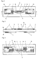
- Figs. 1 to 3 show an example of an embodiment (first embodiment) of the non-contact IC tag according to the invention.
- a non-contact IC tag T1 of the invention includes an IC tag Ta comprising a first insulating substrate 2 , an IC chip 3 provided on one side (first side) 2a of the first insulating substrate 2 and a matching-circuit equipped dipole antenna 1 electrically connected to the IC chip 3, and a first parasitic antenna 6 and a second parasitic antenna 7 spaced with a distance and provided on the other side (second side) 2b of the first insulating substrate 2 .
- the matching-circuit equipped dipole antenna 1 is composed of two antenna sections (a first antenna section 1a and a second antenna section 1b) spaced with a distance, two connecting terminal sections 4 (a first connecting terminal section 4a and a second connecting terminal section 4b) electrically connecting the first antenna section 1a and the second antenna section 1b, respectively, to the IC chip 3 and a matching circuit section 5 electrically connecting the first antenna section 1 a and the second antenna section 1 b.
- the non-contact IC tag T1 of the invention that has a structure as described above also meets the following requirements (1A), (1 B), and (1C).
- the first parasitic antenna 6 and the second parasitic antenna 7 are electrically connected to each other through a connected portion 8.
- the IC tag Ta comprises the IC chip 3 that stores information and the matching-circuit equipped dipole antenna 1 connected to the IC chip 3.
- the IC tag Ta and IC chip 3 may be commercially available non-contact IC tag and IC chip products.
- the IC tag Ta and IC chip 3 are preferably a passive-type non-contact IC tag and an IC chip that use radio wave (microwave) as means of transmission, and more preferably those conforming to ISO/IEC18000-6, and still more preferably those conforming to ISO/IEC18000-6 (Type C).
- the matching-circuit equipped dipole antenna 1 is an antenna provided the matching circuit section 5 to appropriately perform transmission of electric power between the IC chip 3 and the antenna.
- the matching-circuit equipped dipole antenna 1 has the connecting terminal section 4 to electrically connect the antenna to the IC chip 3.
- the connecting terminal section 4 comprises the first connecting terminal section 4a that is connected to one end of the IC chip 3 and the second connecting terminal section 4b that is connected to the other end of the IC chip 3.
- a generally known dipole antenna comprising a meander line and the like may be used.
- the connecting terminal section 4 (the first connecting terminal section 4a and the second connecting terminal section 4b) is a terminal section to electrically connect the IC chip 3 or an IC strap that comprises the IC chip and an extended electrode, to the matching-circuit equipped dipole antenna 1.
- the optimum shape of the connecting terminal section 4 depends on the matching-circuit equipped dipole antenna 1 used, but there are no specific requirements for the connecting terminal section 4 if it can maintain electric connection between the IC chip 3 or the IC strap and the matching-circuit equipped dipole antenna 1.
- the matching circuit 5 serves to maintain electric connection between the first antenna section 1 a and the second antenna section 1b of the matching-circuit equipped dipole antenna 1.
- the matching circuit section 5 aims to perform impedance matching to ensure appropriate transmission of electric power between the IC chip 3 and the matching-circuit equipped dipole antenna 1.
- the matching circuit section 5 may work to maintain direct physical connection between the first antenna section 1a and the second antenna section 1b, but also may work to maintain direct physical connection between the first connecting terminal section 4a and the second connecting terminal section 4b.
- the matching circuit section 5 may work to maintain electrical connect between the first antenna section 1 a and the second antenna section 1 b via the first connecting terminal section 4a and the second connecting terminal section 4b.
- the first parasitic antenna 6 and the second parasitic antenna 7 each are an antenna without a feeding point that serves to assist radio wave transmission function of the matching-circuit equipped dipole antenna 1.
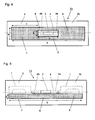
- Figs. 4 and 5 show other different examples of the first embodiment of the non-contact IC tag of the invention.
- Fig. 4 shows a plan view of a second side 2b of a first insulating substrate 2 of a non-contact IC tag T2 of the invention.
- Fig. 5 shows a plan view of a second side 2b of a first insulating substrate 2 of a non-contact IC tag T3 of the invention.
- the plane of a matching-circuit equipped dipole antenna has the same shape as the shape of the plane of the matching-circuit equipped dipole antenna given in the plan view in Fig. 1 that illustrates the plane of the matching-circuit equipped dipole antenna of the non-contact IC tag T1.
- the shape of the plane of a parasitic antenna is different from the shape of the parasitic antenna given in the plan view in Fig. 3 that illustrates the plane of the parasitic antenna of the non-contact IC tag T1.
- the first parasitic antenna 6, the second parasitic antenna 7, and the connected portion 8 meet the following requirements (1A), (1B), and (1C) as in the case of the non-contact IC tag T1 shown in Fig. 3 .
- the first parasitic antenna 6 and the second parasitic antenna 7 are electrically connected to each other through the connected portion 8.
- Fig. 6 shows an example of another embodiment (second embodiment) of the non-contact IC tag according to the invention.
- Fig. 6 shows a plan view of a second side 2b of a first insulating substrate 2 of a non-contact IC tag T4 of the invention.
- the plane of a matching-circuit equipped dipole antenna of the non-contact IC tag T4 shown in Fig. 6 is the same as that of the plane of the matching-circuit equipped dipole antenna given in the plan view in Fig. 1 that illustrates the plane of the matching-circuit equipped dipole antenna of the non-contact IC tag T1.
- the shape of the plane of a parasitic antenna is different from the shape of the parasitic antenna given in the plan view in Fig. 3 that illustrates the plane of the parasitic antenna of the non-contact IC tag T1.
- the first parasitic antenna 6, the second parasitic antenna 7, and the connected portion 8 meet the following requirements (2A), (2B), and (2C).
- the first parasitic antenna 6 and the second parasitic antenna 7 are electrically connected to each other through the connected portion 8.
- the expression “respectively overlap at least partially” in the requirements (1A) and (2A) means that the projection images of the first parasitic antenna 6 and the second parasitic antenna 7 projected onto the first side 2a of the first insulating substrate 2 should not necessarily fit perfectly the first antenna section 1 a and the second antenna section 1b, respectively, of the matching-circuit equipped dipole antenna 1, but may share only a part of the area with the first antenna section 1 a and the second antenna section 1 b.
- the expression "only partially overlap" in the requirement (2C) means that they share only a part of the area with the matching circuit 5 for adjustment of impedance etc.
- the maximum overlap ratio is preferably 50% of the total area that the matching circuit section 5 occupies in the plan view, depending on the shape of each antenna etc. that constitute the non-contact IC tag.
- the non-contact IC tag according to the invention that is illustrated in a concrete manner in the first embodiment and the second embodiment can minimize the influence of the antennae in the IC tag on the impedance fluctuation even when it is attached to a metal member. As a result, electric power necessary to drive the IC chip 3 can be supplied to the IC chip 3 in order to maintain communication between the IC chip 3 and a reader/writer.
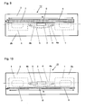
- Figs. 7 to 11 show the shape of the plane of the parasitic antenna of the non-contact IC tag T5, T6, T7, T8, or T9 of the invention, respectively. These represent preferable embodiments of the non-contact IC tag of the invention.
- the shape of the plane of the matching-circuit equipped dipole antenna is the same as that of the plane of the matching-circuit equipped dipole antenna given in the plan view in Fig. 1 that illustrates the plane of the matching-circuit equipped dipole antenna of the non-contact IC tag T1.
- the shape of the plane of the parasitic antenna is different from that of the plane of the parasitic antenna given in the plan view in Fig. 3 that illustrates the plane of the parasitic antenna of the non-contact IC tag T1.
- These preferable embodiments meet the following requirements (3C1) and (3C2).
- the projection images of the first parasitic antenna 6, the second parasitic antenna 7, and the connected portion 8 projected onto the first side 2a of the first insulating substrate 2 do not overlap, or only partially overlap, the matching circuit section 5 of the matching-circuit equipped dipole antenna 1.
- the projection images of the first parasitic antenna 6, the second parasitic antenna 7, and the connected portion 8 projected onto the first side 2a of the first insulating substrate 2 do not overlap the IC chip 3, the first connecting terminal section 4a, and the second connecting terminal section 4b of the matching-circuit equipped dipole antenna 1.
- the non-contact IC tag of the invention in these preferable embodiments has a longer communication distance.
- the shape of the first parasitic antenna 6 and the second parasitic antenna 7 if the requirements are met.
- the entire size of the parasitic antenna composed of the first parasitic antenna 6, the second parasitic antenna 7, and the connected portion 8 is nearly the same as that of the matching-circuit equipped dipole antenna 1.
- the communication distance can be increased by adjusting the size of each parasitic antenna to the frequency used.
- the matching-circuit equipped dipole antenna 1, first parasitic antenna 6, the second parasitic antenna 7, and the connected portion 8 are formed of electric conductors.
- Useful generally-known electric conductors include metals containing at least one of the group of gold, silver, copper, aluminum, zinc, nickel, and tin; conductive polymers such as polyacetylene, polyparaphenylene, polyaniline, polythiophene, and polyparaphenylene vinylene; thermosetting resins composed mainly of polyester resin, phenoxy resin, epoxy resin, polyester resin, etc., containing conductive particles such as particles of metals, alloys, and metal oxides of gold, silver, copper, aluminum, platinum, iron, nickel, tin, zinc, solder, stainless steel, ITO, and ferrite, particles of conductive carbon (including graphite), and resin particles produced by plating the aforementioned particles; and conductive ink produced from UV curable resins and other light curable resins composed mainly of unsaturated polyester resin, polyester acrylate resin, urethane acrylate resin, silicone acrylate resin, epoxy acrylate resin, etc.
- first parasitic antenna 6, the second parasitic antenna 7, and the connected portion 8 are made of the same material.
- the first parasitic antenna 6, the second parasitic antenna 7, and the connected portion 8 may form one seamless body.
- the matching-circuit equipped dipole antenna 1, the first parasitic antenna 6, the second parasitic antenna 7, and the connected portion 8 may be produced by a generally known process such as the etching method to etch metal foil and metal deposition layers, the transfer method to cut out metal foil onto a circuit and fix it on a substrate, and the printing method to perform printing with conductive inks.
- Fig. 12 shows an example of another preferable embodiment of a non-contact IC tag according to the invention.
- Fig. 12 shows the I-I cross section as indicated by the arrows in Fig. 1 , for a non-contact IC tag T10 of the invention that is produced by laminating a second insulating substrate 9 over the IC tag Ta of the non-contact IC tag T1.
- the second insulating substrate 9 covers the matching-circuit equipped dipole antenna 1 in the non-contact IC tag T10, and therefore, if the non-contact IC tag T10 is attached to an object, the second insulating substrate 9 existing between them works to maintain electric insulation between the matching-circuit equipped dipole antenna 1 and the object. This allows the non-contact IC tag T10 to achieve a good communication function.
- the first insulating substrate 2 can work effectively if it can electrically insulate the IC tag Ta from the first parasitic antenna 6, the second parasitic antenna 7, and the connected portion 8.
- the second insulating substrate 9 can work effectively if it can electrically insulate the IC tag Ta from that carries the non-contact IC tag.
- this substrate is preferably in the form of a resin film.
- resins for such film include melt-extrudable materials such as polyester, foamable polyester, polyolefin, polylactic acid, polyamide, polyester amide, polyether, polystyrene, polyphenylene sulfide, polyether ester, polyvinyl chloride, poly(meth)acrylate, etc.
- the film may be in the form of un-stretched film, uni-axially stretched film, or bi-axially stretched film.
- polyester film In view of price and mechanical characteristics, particularly preferable ones include polyester film, polyolefin film, and polyphenylene sulfide film.
- biaxially stretched polyester film is used preferably because it has price advantage, heat resistance, and mechanical characteristics in a good balance.
- the thickness of the first insulating substrate 2 if it can electrically insulate the IC tag Ta from the first parasitic antenna 6, the second parasitic antenna 7, and the connected portion 8.
- the thickness is preferably in the range of 0.001 to 0.25 mm, more preferably 0.01 to 0.125 mm, and still more preferably 0.02 to 0.075 mm.
- the thickness of the second insulating substrate 9 f it can electrically insulate the IC tag Ta from the object. If the thickness is 0.1 mm or more, communication can be maintained even when the non-contact IC tag is attached to a metal member. If the thickness is 0.5 mm or more, it will be possible to increase the communication distance in the case where the non-contact IC tag is attached to a metal member.
- the non-contact IC tag according to the invention is not laminated with the second insulating substrate 9, it is preferable that the first insulating substrate 2, the IC tag Ta, the first parasitic antenna 6, the second parasitic antenna 7, and the connected portion 8 are coated with a resin. If the non-contact IC tag according to the invention is laminated with a second insulating substrate 9, it is preferable that the first insulating substrate 2, the IC tag Ta, the first parasitic antenna 6, the second parasitic antenna 7, the connected portion 8, and the second insulating substrate 9 are coated with a resin. Specifically, it is preferable that the non-contact IC tag according to the invention has both sides coated with a resin or that it is entirely sealed in a resin. The communication distance and durability of the non-contact IC tag is improved, if both sides are coated with a resin or the tag is entirely sealed in a resin.
- Preferable resins for the coating or sealing include melt-extrudable ones including polyester, foamable polyester, polyolefin, polylactic acid, polyamide, polyester amide, polyether, polystyrene, polyphenylene sulfide, polyether ester, polyvinyl chloride, and poly(meth)acrylate.
- a film processed from these resins is used for the covering or sealing of the non-contact IC tag.
- the film may be in the form of un-stretched film, uni-axially stretched film, or bi-axially stretched film.
- the resins those having a dielectric constant of 1 to 3 in the operating radio wave frequency range are used preferably.
- the dielectric constant is more preferably 2 to 3. If the resin has a dielectric constant of 1 to 3, the electric power for the IC chip 3 can be increased while the impedance matching of the IC tag Ta is maintained. This can increase the communication distance of the non-contact IC tag that is used in contact with a metal member.
- the communication distance at 950 MHz is measured.
- an antenna was placed at a height of 90 cm from the floor, whereas a copper plate of 120 mm ⁇ 40 mm ⁇ 0.5 mm was placed at the same height facing the former.
- a non-contact IC tag prepared was attached to the plate by sticking the second insulating substrate at the center of the plate, and measurements were made while changing the distance between the copper plate and a reader/writer to determine the maximum communication distance at which communication between the reader/writer and the IC tag Ta is maintained without errors.
- a reader/writer produced by Omron Corporation (model: V750-BA50CO4-JP) and an antenna produced by Omron Corporation (model: V750-HS01 CA-JP) were used for measurement. Measurements were taken for five samples, and the average of these measurements was taken as the communication distance of the IC tag Ta under test.
- Each sample was cut with a microtome in the thickness direction, and the cross section was observed with a 10,000-power SEM to determine the thickness. Measurements for different items were taken in one sample. Measurements were made at five points in one microscopic field for each sample, and the average of the measurements was taken as the thickness of the component.
- the resulting metalized film was subjected to wet etching to produce a parasitic antenna having a shape as shown in Fig. 3 .
- the first parasitic antenna 6, second parasitic antenna 7, and connected portion 8 were thus formed.
- a UHF tag Ta (ALN-9540-Squiggle supplied by Alien) having an IC chip 3 and a matching-circuit equipped dipole antenna 1 was prepared.
- An acrylic plate having a thickness of 1 mm was used as a second insulating substrate 9, and the UHF tag Ta was adhered to it. Then, the first side 2a of the first insulating substrate 2 was adhered to that side of the second insulating substrate 9 which carried the UHF tag Ta.
- the projection images of the first parasitic antenna 6 and the second parasitic antenna 7 projected onto the second insulating substrate 9 respectively overlap at least partially the first antenna section 1a and the second antenna section 1b of the matching-circuit equipped dipole antenna 1.
- the resulting non-contact IC tag T1 had a communication distance of 830 mm.
- the metalized film obtained in Example 1 was subjected to wet etching to produce a parasitic antenna having a shape as shown in Fig. 4 .
- the first parasitic antenna 6, the second parasitic antenna 7, and the connected portion 8 were thus formed.
- the resulting metalized film and the second insulating substrate produced in Example 1 were fixed together by the same procedure as in Example 1 to provide a non-contact IC tag T2.
- the resulting non-contact IC tag T2 had a communication distance of 690 mm.
- Example 1 The metalized film obtained in Example 1 was subjected to wet etching to produce a parasitic antenna having a shape as shown in Fig. 5 .
- the first parasitic antenna 6, the second parasitic antenna 7, and the connected portion 8 were thus formed.
- the resulting metalized film and the second insulating substrate produced in Example 1 were fixed together by the same procedure as in Example 1 to provide a non-contact IC tag T3.
- the resulting non-contact IC tag T3 had a communication distance of 790 mm.
- a bi-axially stretched polyethylene terephthalate film (Lumiror (registered trademark) S10 supplied by Toray Industries, Inc.) having a thickness of 0.05 mm was used as the first insulating substrate 2.
- an aluminum layer having a thickness of 0.002 mm was formed by electron beam (EB) deposition over one side of the first insulating substrate 2.
- the resulting metalized film was subjected to wet etching to produce a parasitic antenna having a shape as shown in Fig. 6 .
- the first parasitic antenna 6, the second parasitic antenna 7, and the connected portion 8 were thus formed.
- a UHF tag Ta (ALN-9540-Squiggle supplied by Alien) having an IC chip 3 and a matching-circuit equipped dipole antenna 1 was prepared.
- An acrylic plate having a thickness of 1 mm was used as a second insulating substrate 9, and the UHF tag Ta was adhered to it. Then, the first side 2a of the first insulating substrate 2 was adhered to that side of the second insulating substrate 9 which carried the UHF tag Ta.
- the projection images of the first parasitic antenna 6 and the second parasitic antenna 7 projected onto the second insulating substrate 9 respectively overlap at least partially the first antenna section 1a and the second antenna section 1 b of the matching-circuit equipped dipole antenna 1.
- the resulting non-contact IC tag T4 had a communication distance of 880 mm.
- a bi-axially stretched polyethylene terephthalate film (Lumiror (registered trademark) S10 supplied by Toray Industries, Inc.) having a thickness of 0.05 mm was used as the first insulating substrate 2.
- an aluminum layer having a thickness of 0.002 mm was formed by electron beam (EB) deposition over one side of the first insulating substrate 2.
- the resulting metalized film was subjected to wet etching to produce a parasitic antenna having a shape as shown in Fig. 8 .
- the first parasitic antenna 6, the second parasitic antenna 7, and connected portion 8 were thus formed.
- a UHF tag Ta (ALN-9540-Squiggle supplied by Alien) having an IC chip 3 and a matching-circuit equipped dipole antenna 1 was prepared.
- An acrylic plate having a thickness of 1 mm was used as the second insulating substrate 9, and the UHF tag Ta was adhered to it. Then, the first side 2a of the first insulating substrate 2 was adhered to that side of the second insulating substrate 9 which carried the UHF tag Ta.
- the projection images of the first parasitic antenna 6 and the second parasitic antenna 7 projected onto the second insulating substrate 9 respectively overlap at least partially the first antenna section 1a and the second antenna section 1b of the matching-circuit equipped dipole antenna 1.
- the projection images of the first parasitic antenna 6, the second parasitic antenna 7, and the connected portion 8 projected onto the second insulating substrate 9 do not overlap, or only partially overlap, the matching circuit section 5 of the matching-circuit equipped dipole antenna 1.
- the resulting non-contact IC tag T6 had a communication distance of 840 mm.
- Example 5 The metalized film obtained in Example 5 was subjected to wet etching to produce a parasitic antenna having a shape as shown in Fig. 10 .
- the first parasitic antenna 6, the second parasitic antenna 7, and the connected portion 8 were thus formed.
- the resulting metalized film and the second insulating substrate produced in Example 5 were fixed together by the same procedure as in Example 5 to provide a non-contact IC tag T8.
- the resulting non-contact IC tag T8 had a communication distance of 800 mm.
- the metalized film obtained in Example 5 was subjected to wet etching to produce a parasitic antenna having a shape as shown in Fig. 11 .
- the resulting metalized film and the second insulating substrate produced in Example 5 were fixed together by the same procedure as in Example 5 to provide a non-contact IC tag T9.
- the resulting non-contact IC tag T9 had a communication distance of 1340 mm.
- a non-contact IC tag was produced by carrying out the same procedure as in Example 7 except for the following: fixing the first insulating substrate 2, the IC tag Ta, the first parasitic antenna 6, the second parasitic antenna 7, the connected portion 8, and the second insulating substrate 9, followed by coating the first insulating substrate 2, the IC tag Ta, the first parasitic antenna 6, the second parasitic antenna 7, the connected portion 8, and the second insulating substrate 9 with a convex-shape polyester resin layer having a thickness of 0.25 mm and a polyester resin layer having a thickness of 0.25 mm.
- the resulting non-contact IC tag had a communication distance of 2450 mm.
- the resulting non-contact IC tag had a communication distance of 110 mm. Comparative example 2
- a bi-axially stretched polyethylene terephthalate film (Lumiror S10 supplied by Toray Industries, Inc.) having a thickness of 0.05 mm was used as the first insulating substrate 2.
- the resulting metalized film was subjected to wet etching to produce a parasitic antenna having a shape as shown in Fig. 5 .
- the first parasitic antenna 6, the second parasitic antenna 7, and the connected portion 8 were thus formed.
- a UHF tag Ta (ALN-9540-Squiggle supplied by Alien) having an IC chip 3 and a matching-circuit equipped dipole antenna 1 was prepared.
- An acrylic plate having a thickness of 1 mm was used as the second insulating substrate 9, and the UHF tag Ta was adhered to it. Then, the first side 2a of the first insulating substrate 2 was adhered to that side of the second insulating substrate 9 which carried the UHF tag Ta.
- a bi-axially stretched polyethylene terephthalate film (Lumiror S10 supplied by Toray Industries, Inc.) having a thickness of 0.05 mm was used as the first insulating substrate 2.
- the resulting metalized film was subjected to wet etching to produce a parasitic antenna having a shape as shown in Fig. 11 .
- the first parasitic antenna 6, the second parasitic antenna 7, and the connected portion 8 were thus formed.
- a slit was made in the connected portion 8 to prevent conduction between the first parasitic antenna 6 and the second parasitic antenna 7.
- a UHF tag Ta (ALN-9540-Squiggle supplied by Alien) having an IC chip 3 and a matching-circuit equipped dipole antenna 1 was prepared.
- An acrylic plate having a thickness of 1 mm was used as the second insulating substrate 9, and the UHF tag Ta was adhered to it. Then, the first side 2a of the first insulating substrate 2 was adhered to that side of the second insulating substrate 9 which carried the UHF tag Ta.
- the projection images of the first parasitic antenna 6 and the second parasitic antenna 7 projected onto the second insulating substrate 9 respectively overlap at least partially the first antenna section 1a and the second antenna section 1 b of the matching-circuit equipped dipole antenna 1.
- the resulting non-contact IC tag had a communication distance of 500 mm.
- a bi-axially stretched polyethylene terephthalate film (Lumiror S10 supplied by Toray Industries, Inc.) having a thickness of 0.05 mm was used as the first insulating substrate 2.
- the resulting metalized film was subjected to wet etching to produce a parasitic antenna having a shape as shown in Fig. 11 .
- a UHF tag Ta (ALN-9540-Squiggle supplied by Alien) having an IC chip 3 and a matching-circuit equipped dipole antenna was prepared.
- An acrylic plate having a thickness of 1 mm was used as the second insulating substrate 9, and the UHF tag Ta was adhered to it. Then, the first side 2a of the first insulating substrate 2 was adhered to that side of the second insulating substrate 9 which carried the UHF tag Ta.
- the projection images of the first parasitic antenna 6 and the second parasitic antenna 7 projected onto the second insulating substrate 9 respectively overlap at least partially the first antenna section 1a and the second antenna section 1b of the matching-circuit equipped dipole antenna 1.
- the projection images of the first parasitic antenna 6 and the second parasitic antenna 7 projected onto the second insulating substrate 9 do not overlap, or only partially overlap, the matching circuit section 5 of the matching-circuit equipped dipole antenna 1.
- the resulting non-contact IC tag had a communication distance of 640 mm.
- Element B Projection images of first parasitic antenna, second parasitic antenna, and connected portion projected onto second insulating substrate overlap matching circuit section of dipole antenna.
- Element C First parasitic antenna and second parasitic antenna are electrically connected.
- Element D Communication distance (mm)
- Example 4 From comparison between Example 4 and Comparative example 2, it is found that if the non-contact IC tag is produced so that the projection images of the first parasitic antenna 6, the second parasitic antenna 7, and the connected portion 8 projected onto the first side 2a of the first insulating substrate 2 do not overlap, or only partially overlap, the matching circuit section 5 of the matching-circuit equipped dipole antenna 1 of the IC tag Ta, the non-contact IC tag can maintain a sufficient communication function even when the non-contact IC tag is attached to a metal member.
- Example 7 From comparison between Example 7 and Comparative examples 3 and 4, it is found that if the non-contact IC tag is produced so that electric conduction between the first parasitic antenna 6 and the second parasitic antenna 7 is maintained through the connected portion 8, this serves to increase the communication distance of the non-contact IC tag that is used in contact with a metal member.
- Example 7 From comparison Example 7 and Example 8, it is found that if the non-contact IC tag is produced so that the first insulating substrate 2, the IC tag Ta, the first parasitic antenna 6, the second parasitic antenna 7, the connected portion 8, and the second insulating substrate 9 are coated with a resin, this serves to further increase the communication distance of the non-contact IC tag that is used in contact with a metal member.
- the communication function of the IC chip will not deteriorate even when the IC tag is in direct contact with a metal object.
- the non-contact IC tag according to the invention serves for efficient management of metal objects.
Landscapes
- Details Of Aerials (AREA)
- Variable-Direction Aerials And Aerial Arrays (AREA)
Abstract
Description
- The present invention relates to a non-contact IC tag. The invention relates to a non-contact IC tag whose communication performance is little influenced by a metal member to which it is stuck. In particular, the invention relates to a passive-type non-contact IC tag that uses radio wave (microwave) to achieve transmission.
- A non-contact IC tag comprises an antenna circuit and an IC chip (chip with a built-in integrated circuit) that stores required information. A non-contact IC tag is placed at a distance, for instance stuck on an object located at a distance. Thus, the information stored in one or more non-contact IC tags are obtained through radio transmission between these non-contact IC tags and an external antenna located at a distance from them. The information acquisition using non-contact IC tags has good features that cannot be achieved by the information acquisition mechanism based on bar codes, and in particular, their use is promoted in the field of distribution of merchandise.
- Some common non-contact IC tags suffer serious influence on its communication performance caused by the object that carries them. If the tag-carrying object is metal, in particular, the communication between the non-contact IC tag installed on it and the external antenna can be impeded seriously. Specifically, if a non-contact IC tag is installed on a metal member, the impedance matching between the IC chip in the non-contact IC tag and the antenna in the non-contact IC tag can deteriorate largely.
- As a result, the electric power gained through the radio wave resonance in the antenna will not be supplied to the IC chip efficiently, failing to obtain electric power required to drive the IC chip. This makes impossible to achieve information transmission between the non-contact IC tag and a reader/writer located at a distance from the non-contact IC tag. This phenomenon will be particularly noticeable in cases where radio wave (microwave) is used as transmission means in combination with passive-type non-contact IC tags which do not use a battery. Various non-contact IC tags have been developed to solve this problem. Of such IC tags, well-known ones include the following.
- (1) An IC tag comprising a first antenna formed on a first insulating material and a second antenna formed with a second insulating material in between, wherein the length of the second antenna is adjusted to an appropriate value to allow the IC tag to perform communication when located on a metal member (Patent Literature 1).
- (2) An IC tag comprising a plastic base with a dipole antenna on one side and a metal layer on the other side wherein stripe-like portions of the metal layer extending in the direction perpendicular to the dipole antenna are removed (Patent Literature 2).
- (3) An IC tag comprising a foamed resin inserted between the IC tag and a metal member carrying the IC tag so that the contact between the IC tag and the metal member is avoided to reduce the influence of the metal to make communication possible (Patent Literature 3).
- (4) An IC tag comprising a magnetic material inserted between the IC tag and a metal member carrying the IC tag to decrease the influence of the metal to improve the communication (Patent Literature 4).
-
- Patent Literature 1:
JP 2005-210676 A - Patent Literature 2:
JP 2007-311955 A - Patent Literature 3:
JP 2007-241788 A - Patent Literature 4:
J P 2007-277080 A - Use of the aforementioned various IC tags permits communication when these IC tags are installed on a metal member. However, in the IC tags (1) and (2), it is difficult to supply electric power to the IC chip, leading to a short communication distance, which is a problem. In the IC tag (3), the resin has to be thick to ensure a long communication distance, leading to the problem of difficulty in ensuring long distance communication, hence difficulty in developing thin IC tags. In the IC tag (4), furthermore, the magnetic material is expensive, leading to the problem of difficulty in producing IC tags at low cost.
- In view of this state of prior art, the invention aims to provide a non-contact IC tag that is low-priced, thin, and able to perform long distance communication even when installed on a metal member. The invention particularly aims to provide a non-contact IC tag that can serve to construct a passive-type non-contact IC tag that uses radio wave (microwave) for transmission.
- Described below is an embodiment (first embodiment) of the non-contact IC tag according to the invention to solve the problems.
- A non-contact IC tag including an IC tag comprising a first insulating substrate, an IC chip fixed on one side of the first insulating substrate and a matching-circuit equipped dipole antenna electrically connected to the IC chip, and a first parasitic antenna and a second parasitic antenna spaced with a distance and fixed on the other side of the first insulating substrate, wherein the matching-circuit equipped dipole antenna has two antenna sections spaced with a distance, two connecting terminal sections each electrically connecting each of the two antenna sections to the IC chip, and a matching circuit section electrically connecting the two antenna sections to each other, and wherein
- (1-a) the projection images of the first parasitic antenna and the second parasitic antenna projected onto the one side of the first insulating substrate respectively overlap at least partially the two antenna sections of the matching-circuit equipped dipole antenna,
- (1-b) the first parasitic antenna and the second parasitic antenna are electrically connected to each other through a connected portion, and in addition,
- (1-c) the projection images of the first parasitic antenna, the second parasitic antenna, and the connected portion projected onto the one side of the first insulating substrate do not overlap the IC chip and the two connecting terminal sections of the matching-circuit equipped dipole antenna.
- Described below is another embodiment (second embodiment) of the non-contact IC tag according to the invention to solve the problem.
- A non-contact IC tag including an IC tag comprising a first insulating substrate, an IC chip fixed on one side of the first insulating substrate and a matching-circuit equipped dipole antenna electrically connected to the IC chip, and a first parasitic antenna and a second parasitic antenna spaced with a distance and fixed on the other side of the first insulating substrate, wherein the matching-circuit equipped dipole antenna has two antenna sections spaced with a distance, two connecting terminal sections each electrically connecting each of the two antenna sections to the IC chip, and a matching circuit section electrically connecting the two antenna sections to each other, and wherein
- (2-a) the projection images of the first parasitic antenna and the second parasitic antenna projected onto the one side of the first insulating substrate respectively overlap at least partially the two antenna sections of the matching-circuit equipped dipole antenna,
- (2-b) the first parasitic antenna and the second parasitic antenna are electrically connected to each other through a connected portion, and in addition,
- (2-c) the projection images of the first parasitic antenna, the second parasitic antenna, and the connected portion projected onto the one side of the first insulating substrate do not overlap, or only partially overlap, the matching circuit section of the matching-circuit equipped dipole antenna.
- In the second embodiment, it is preferable that the projection images of the first parasitic antenna, the second parasitic antenna, and the connected portion projected onto the one side of the first insulating substrate do not overlap the matching circuit section of the matching-circuit equipped dipole antenna.
- In the second embodiment, it is preferable that the projection images of the first parasitic antenna, the second parasitic antenna, and the connected portion projected onto the one side of the first insulating substrate do not overlap the IC chip and the two connecting terminal sections of the matching-circuit equipped dipole antenna.
- In the first embodiment and the second embodiment, it is preferable that the first insulating substrate is in the form of a resin film.
- In the first embodiment and the second embodiment, it is preferable that a second insulating substrate is laminated over the one side of the first insulating substrate.
- In the first embodiment and the second embodiment, it is preferable that the first insulating substrate, the IC tag, the first parasitic antenna, the second parasitic antenna, and the connected portion are coated with a resin.
- In the embodiment wherein the second insulating substrate is laminated, the first insulating substrate, the IC tag, the first parasitic antenna, the second parasitic antenna, the connected portion, and the second insulating substrate are coated with a resin.
- If a non-contact IC tag according to the invention is used, normal communication can be maintained between the non-contact IC tag and a reader/writer even when the non-contact IC tag is attached to a metal member. If the non-contact IC tag according to the invention is used, a larger electric power is supplied to an IC chip contained there to increase the communication distance between the IC chip and the reader/writer, compared with a conventional non-contact IC tag alone is attached to a metal member. In particular, the non-contact IC tag according to the invention is preferably applied to a passive-type non-contact IC tag that uses radio wave (microwave) as means of transmission.
-
-
Fig. 1 shows a schematic plan view of the plane of a matching-circuit equipped dipole antenna in an embodiment (first embodiment) of the non-contact IC tag of the invention. -
Fig. 2 shows the I-I cross section indicated by the arrows inFig. 1 . -
Fig. 3 shows a schematic plan view of an example of the plane of the parasitic antenna of the non-contact IC tag illustrated inFig. 1 . -
Fig. 4 shows a schematic plan view of another example of the plane of the parasitic antenna of the non-contact IC tag illustrated inFig. 1 . -
Fig. 5 shows a schematic plan view of still another example of the plane of the parasitic antenna of the non-contact IC tag illustrated inFig. 1 . -
Fig. 6 shows a schematic plan view of an example of the plane of the parasitic antenna in another embodiment (second embodiment) of the non-contact IC tag of the invention. -
Fig. 7 shows a schematic plan view of a preferable example of the plane of the parasitic antenna of the non-contact IC tag of the invention. -
Fig. 8 shows a schematic plan view of another preferable example of the plane of the parasitic antenna of the non-contact IC tag of the invention. -
Fig. 9 shows a schematic plan view of still another preferable example of the plane of the parasitic antenna of the non-contact IC tag of the invention. -
Fig. 10 shows a schematic plan view of still another preferable example of the plane of the parasitic antenna of the non-contact IC tag of the invention. -
Fig. 11 shows a schematic plan view of still another preferable example of the plane of the parasitic antenna of the non-contact IC tag of the invention. -
Fig. 12 shows the I-I cross section as indicated by the arrows inFig. 1 , for a non-contact IC tag according to the invention that is produced by laminating a second insulating substrate over the IC tag of the non-contact IC tag. -
Figs. 1 to 3 show an example of an embodiment (first embodiment) of the non-contact IC tag according to the invention. - In
Figs. 1 to 3 , a non-contact IC tag T1 of the invention includes an IC tag Ta comprising a first insulatingsubstrate 2 , anIC chip 3 provided on one side (first side) 2a of the first insulatingsubstrate 2 and a matching-circuit equippeddipole antenna 1 electrically connected to theIC chip 3, and a firstparasitic antenna 6 and a secondparasitic antenna 7 spaced with a distance and provided on the other side (second side) 2b of the first insulatingsubstrate 2 . - The matching-circuit equipped
dipole antenna 1 is composed of two antenna sections (afirst antenna section 1a and asecond antenna section 1b) spaced with a distance, two connecting terminal sections 4 (a first connectingterminal section 4a and a second connectingterminal section 4b) electrically connecting thefirst antenna section 1a and thesecond antenna section 1b, respectively, to theIC chip 3 and amatching circuit section 5 electrically connecting thefirst antenna section 1 a and thesecond antenna section 1 b. - The non-contact IC tag T1 of the invention that has a structure as described above also meets the following requirements (1A), (1 B), and (1C).
- (1A) The projection images of the first
parasitic antenna 6 and the secondparasitic antenna 7 projected onto thefirst side 2a of the first insulatingsubstrate 2 respectively overlap at least partially thefirst antenna section 1a and thesecond antenna section 1 b of the matching-circuit equippeddipole antenna 1. - (1 B) The first
parasitic antenna 6 and the secondparasitic antenna 7 are electrically connected to each other through aconnected portion 8. - (1C) The projection images of the first
parasitic antenna 6, the secondparasitic antenna 7, and theconnected portion 8 projected onto thefirst side 2a of the first insulatingsubstrate 2 do not overlap theIC chip 3, and the first connectingterminal section 4a and the second connectingterminal section 4b of the matching-circuit equippeddipole antenna 1. - The IC tag Ta comprises the
IC chip 3 that stores information and the matching-circuit equippeddipole antenna 1 connected to theIC chip 3. The IC tag Ta andIC chip 3 may be commercially available non-contact IC tag and IC chip products. The IC tag Ta andIC chip 3 are preferably a passive-type non-contact IC tag and an IC chip that use radio wave (microwave) as means of transmission, and more preferably those conforming to ISO/IEC18000-6, and still more preferably those conforming to ISO/IEC18000-6 (Type C). - The matching-circuit equipped
dipole antenna 1 is an antenna provided thematching circuit section 5 to appropriately perform transmission of electric power between theIC chip 3 and the antenna. - The matching-circuit equipped
dipole antenna 1 has the connectingterminal section 4 to electrically connect the antenna to theIC chip 3. The connectingterminal section 4 comprises the first connectingterminal section 4a that is connected to one end of theIC chip 3 and the second connectingterminal section 4b that is connected to the other end of theIC chip 3. As the matching-circuit equippeddipole antenna 1 of this structure, a generally known dipole antenna comprising a meander line and the like may be used. - The connecting terminal section 4 (the first connecting
terminal section 4a and the second connectingterminal section 4b) is a terminal section to electrically connect theIC chip 3 or an IC strap that comprises the IC chip and an extended electrode, to the matching-circuit equippeddipole antenna 1. The optimum shape of the connectingterminal section 4 depends on the matching-circuit equippeddipole antenna 1 used, but there are no specific requirements for the connectingterminal section 4 if it can maintain electric connection between theIC chip 3 or the IC strap and the matching-circuit equippeddipole antenna 1. - The
matching circuit 5 serves to maintain electric connection between thefirst antenna section 1 a and thesecond antenna section 1b of the matching-circuit equippeddipole antenna 1. Thematching circuit section 5 aims to perform impedance matching to ensure appropriate transmission of electric power between theIC chip 3 and the matching-circuit equippeddipole antenna 1. Thematching circuit section 5 may work to maintain direct physical connection between thefirst antenna section 1a and thesecond antenna section 1b, but also may work to maintain direct physical connection between the first connectingterminal section 4a and the second connectingterminal section 4b. Thus, thematching circuit section 5 may work to maintain electrical connect between thefirst antenna section 1 a and thesecond antenna section 1 b via the first connectingterminal section 4a and the second connectingterminal section 4b. - The first
parasitic antenna 6 and the secondparasitic antenna 7 each are an antenna without a feeding point that serves to assist radio wave transmission function of the matching-circuit equippeddipole antenna 1. -
Figs. 4 and 5 show other different examples of the first embodiment of the non-contact IC tag of the invention.Fig. 4 shows a plan view of asecond side 2b of a first insulatingsubstrate 2 of a non-contact IC tag T2 of the invention.Fig. 5 shows a plan view of asecond side 2b of a first insulatingsubstrate 2 of a non-contact IC tag T3 of the invention. - In each of the non-contact IC tag T2 shown in
Fig. 4 and the non-contact IC tag T3 shown inFig. 5 , the plane of a matching-circuit equipped dipole antenna has the same shape as the shape of the plane of the matching-circuit equipped dipole antenna given in the plan view inFig. 1 that illustrates the plane of the matching-circuit equipped dipole antenna of the non-contact IC tag T1. - In each of the non-contact IC tag T2 shown in
Fig. 4 and the non-contact IC tag T3 shown inFig. 5 , the shape of the plane of a parasitic antenna is different from the shape of the parasitic antenna given in the plan view inFig. 3 that illustrates the plane of the parasitic antenna of the non-contact IC tag T1. - In the non-contact IC tag T2 shown in
Fig. 4 and the non-contact IC tag T3 shown inFig. 5 , the firstparasitic antenna 6, the secondparasitic antenna 7, and theconnected portion 8 meet the following requirements (1A), (1B), and (1C) as in the case of the non-contact IC tag T1 shown inFig. 3 . - (1A) The projection images of the first
parasitic antenna 6 and the secondparasitic antenna 7 projected onto thefirst side 2a of the first insulatingsubstrate 2 respectively overlap at least partially thefirst antenna section 1a and thesecond antenna section 1b of the matching-circuit equippeddipole antenna 1. - (1 B) The first
parasitic antenna 6 and the secondparasitic antenna 7 are electrically connected to each other through the connectedportion 8. - (1C) The projection images of the first
parasitic antenna 6, the secondparasitic antenna 7, and theconnected portion 8 projected onto thefirst side 2a of the first insulatingsubstrate 2 do not overlap theIC chip 3 and the connectingterminal section 4 of the matching-circuit equippeddipole antenna 1. -
Fig. 6 shows an example of another embodiment (second embodiment) of the non-contact IC tag according to the invention.Fig. 6 shows a plan view of asecond side 2b of a first insulatingsubstrate 2 of a non-contact IC tag T4 of the invention. The plane of a matching-circuit equipped dipole antenna of the non-contact IC tag T4 shown inFig. 6 is the same as that of the plane of the matching-circuit equipped dipole antenna given in the plan view inFig. 1 that illustrates the plane of the matching-circuit equipped dipole antenna of the non-contact IC tag T1. - In the non-contact IC tag T4 shown in
Fig. 6 , the shape of the plane of a parasitic antenna is different from the shape of the parasitic antenna given in the plan view inFig. 3 that illustrates the plane of the parasitic antenna of the non-contact IC tag T1. - In the non-contact IC tag T4 shown in
Fig. 6 , the firstparasitic antenna 6, the secondparasitic antenna 7, and theconnected portion 8 meet the following requirements (2A), (2B), and (2C). - (2A) The projection images of the first
parasitic antenna 6 and the secondparasitic antenna 7 projected onto thefirst side 2a of the first insulatingsubstrate 2 respectively overlap at least partially thefirst antenna section 1a and thesecond antenna section 1b of the matching-circuit equippeddipole antenna 1. - (2B) The first
parasitic antenna 6 and the secondparasitic antenna 7 are electrically connected to each other through the connectedportion 8. - (2C) The projection images of the first
parasitic antenna 6, the secondparasitic antenna 7, and theconnected portion 8 projected onto thefirst side 2a of the first insulatingsubstrate 2 do not overlap, or only partially overlap, thematching circuit section 5 of the matching-circuit equippeddipole antenna 1. - The expression "respectively overlap at least partially" in the requirements (1A) and (2A) means that the projection images of the first
parasitic antenna 6 and the secondparasitic antenna 7 projected onto thefirst side 2a of the first insulatingsubstrate 2 should not necessarily fit perfectly thefirst antenna section 1 a and thesecond antenna section 1b, respectively, of the matching-circuit equippeddipole antenna 1, but may share only a part of the area with thefirst antenna section 1 a and thesecond antenna section 1 b. - The expression "only partially overlap" in the requirement (2C) means that they share only a part of the area with the
matching circuit 5 for adjustment of impedance etc. In the case of such partial overlapping, the maximum overlap ratio is preferably 50% of the total area that thematching circuit section 5 occupies in the plan view, depending on the shape of each antenna etc. that constitute the non-contact IC tag. - The non-contact IC tag according to the invention that is illustrated in a concrete manner in the first embodiment and the second embodiment can minimize the influence of the antennae in the IC tag on the impedance fluctuation even when it is attached to a metal member. As a result, electric power necessary to drive the
IC chip 3 can be supplied to theIC chip 3 in order to maintain communication between theIC chip 3 and a reader/writer. -
Figs. 7 to 11 show the shape of the plane of the parasitic antenna of the non-contact IC tag T5, T6, T7, T8, or T9 of the invention, respectively. These represent preferable embodiments of the non-contact IC tag of the invention. - In each of the non-contact IC tags T5, T6, T7, T8, and T9 shown in
Figs. 7 to 11 , the shape of the plane of the matching-circuit equipped dipole antenna is the same as that of the plane of the matching-circuit equipped dipole antenna given in the plan view inFig. 1 that illustrates the plane of the matching-circuit equipped dipole antenna of the non-contact IC tag T1. - In each of the non-contact IC tags T5, T6, T7, T8, and T9 shown in
Figs. 7 to 11 , the shape of the plane of the parasitic antenna is different from that of the plane of the parasitic antenna given in the plan view inFig. 3 that illustrates the plane of the parasitic antenna of the non-contact IC tag T1. These preferable embodiments meet the following requirements (3C1) and (3C2). - (3C1) In addition to the requirement (1C) met by the non-contact IC tag of the first embodiment, the projection images of the first
parasitic antenna 6, the secondparasitic antenna 7, and theconnected portion 8 projected onto thefirst side 2a of the first insulatingsubstrate 2 do not overlap, or only partially overlap, thematching circuit section 5 of the matching-circuit equippeddipole antenna 1. - (3C2) In addition to the requirement (2C) met by the non-contact IC tag of the second embodiment, the projection images of the first
parasitic antenna 6, the secondparasitic antenna 7, and theconnected portion 8 projected onto thefirst side 2a of the first insulatingsubstrate 2 do not overlap theIC chip 3, the first connectingterminal section 4a, and the second connectingterminal section 4b of the matching-circuit equippeddipole antenna 1. - The non-contact IC tag of the invention in these preferable embodiments has a longer communication distance.
- There are no specific limitations on the shape of the first
parasitic antenna 6 and the secondparasitic antenna 7 if the requirements are met. For size reduction, it is preferable that the entire size of the parasitic antenna composed of the firstparasitic antenna 6, the secondparasitic antenna 7, and theconnected portion 8 is nearly the same as that of the matching-circuit equippeddipole antenna 1. Furthermore, the communication distance can be increased by adjusting the size of each parasitic antenna to the frequency used. - The matching-circuit equipped
dipole antenna 1, firstparasitic antenna 6, the secondparasitic antenna 7, and theconnected portion 8 are formed of electric conductors. - Useful generally-known electric conductors include metals containing at least one of the group of gold, silver, copper, aluminum, zinc, nickel, and tin; conductive polymers such as polyacetylene, polyparaphenylene, polyaniline, polythiophene, and polyparaphenylene vinylene; thermosetting resins composed mainly of polyester resin, phenoxy resin, epoxy resin, polyester resin, etc., containing conductive particles such as particles of metals, alloys, and metal oxides of gold, silver, copper, aluminum, platinum, iron, nickel, tin, zinc, solder, stainless steel, ITO, and ferrite, particles of conductive carbon (including graphite), and resin particles produced by plating the aforementioned particles; and conductive ink produced from UV curable resins and other light curable resins composed mainly of unsaturated polyester resin, polyester acrylate resin, urethane acrylate resin, silicone acrylate resin, epoxy acrylate resin, etc.
- It is preferable that the first
parasitic antenna 6, the secondparasitic antenna 7, and theconnected portion 8 are made of the same material. The firstparasitic antenna 6, the secondparasitic antenna 7, and theconnected portion 8 may form one seamless body. - The matching-circuit equipped
dipole antenna 1, the firstparasitic antenna 6, the secondparasitic antenna 7, and theconnected portion 8 may be produced by a generally known process such as the etching method to etch metal foil and metal deposition layers, the transfer method to cut out metal foil onto a circuit and fix it on a substrate, and the printing method to perform printing with conductive inks. -
Fig. 12 shows an example of another preferable embodiment of a non-contact IC tag according to the invention.Fig. 12 shows the I-I cross section as indicated by the arrows inFig. 1 , for a non-contact IC tag T10 of the invention that is produced by laminating a second insulating substrate 9 over the IC tag Ta of the non-contact IC tag T1. The second insulating substrate 9 covers the matching-circuit equippeddipole antenna 1 in the non-contact IC tag T10, and therefore, if the non-contact IC tag T10 is attached to an object, the second insulating substrate 9 existing between them works to maintain electric insulation between the matching-circuit equippeddipole antenna 1 and the object. This allows the non-contact IC tag T10 to achieve a good communication function. - The first insulating
substrate 2 can work effectively if it can electrically insulate the IC tag Ta from the firstparasitic antenna 6, the secondparasitic antenna 7, and theconnected portion 8. The second insulating substrate 9 can work effectively if it can electrically insulate the IC tag Ta from that carries the non-contact IC tag. - In view of strength and weight, this substrate is preferably in the form of a resin film. Useful resins for such film include melt-extrudable materials such as polyester, foamable polyester, polyolefin, polylactic acid, polyamide, polyester amide, polyether, polystyrene, polyphenylene sulfide, polyether ester, polyvinyl chloride, poly(meth)acrylate, etc. The film may be in the form of un-stretched film, uni-axially stretched film, or bi-axially stretched film.
- In view of price and mechanical characteristics, particularly preferable ones include polyester film, polyolefin film, and polyphenylene sulfide film. In particular, biaxially stretched polyester film is used preferably because it has price advantage, heat resistance, and mechanical characteristics in a good balance.
- There are no specific requirements for the thickness of the first insulating
substrate 2 if it can electrically insulate the IC tag Ta from the firstparasitic antenna 6, the secondparasitic antenna 7, and theconnected portion 8. In view of flexibility and strength, the thickness is preferably in the range of 0.001 to 0.25 mm, more preferably 0.01 to 0.125 mm, and still more preferably 0.02 to 0.075 mm. - There are no specific requirements for the thickness of the second insulating substrate 9 f it can electrically insulate the IC tag Ta from the object. If the thickness is 0.1 mm or more, communication can be maintained even when the non-contact IC tag is attached to a metal member. If the thickness is 0.5 mm or more, it will be possible to increase the communication distance in the case where the non-contact IC tag is attached to a metal member.
- If the non-contact IC tag according to the invention is not laminated with the second insulating substrate 9, it is preferable that the first insulating
substrate 2, the IC tag Ta, the firstparasitic antenna 6, the secondparasitic antenna 7, and theconnected portion 8 are coated with a resin. If the non-contact IC tag according to the invention is laminated with a second insulating substrate 9, it is preferable that the first insulatingsubstrate 2, the IC tag Ta, the firstparasitic antenna 6, the secondparasitic antenna 7, theconnected portion 8, and the second insulating substrate 9 are coated with a resin. Specifically, it is preferable that the non-contact IC tag according to the invention has both sides coated with a resin or that it is entirely sealed in a resin. The communication distance and durability of the non-contact IC tag is improved, if both sides are coated with a resin or the tag is entirely sealed in a resin. - Preferable resins for the coating or sealing include melt-extrudable ones including polyester, foamable polyester, polyolefin, polylactic acid, polyamide, polyester amide, polyether, polystyrene, polyphenylene sulfide, polyether ester, polyvinyl chloride, and poly(meth)acrylate.
- It is preferable that a film processed from these resins is used for the covering or sealing of the non-contact IC tag. The film may be in the form of un-stretched film, uni-axially stretched film, or bi-axially stretched film.
- Of these resins, those having a dielectric constant of 1 to 3 in the operating radio wave frequency range are used preferably. The dielectric constant is more preferably 2 to 3. If the resin has a dielectric constant of 1 to 3, the electric power for the
IC chip 3 can be increased while the impedance matching of the IC tag Ta is maintained. This can increase the communication distance of the non-contact IC tag that is used in contact with a metal member. - The invention is described more specifically below with reference to examples and comparative examples.
- The communication distance at 950 MHz is measured. In an anechoic chamber for the 3m method, an antenna was placed at a height of 90 cm from the floor, whereas a copper plate of 120 mm × 40 mm × 0.5 mm was placed at the same height facing the former. Then a non-contact IC tag prepared was attached to the plate by sticking the second insulating substrate at the center of the plate, and measurements were made while changing the distance between the copper plate and a reader/writer to determine the maximum communication distance at which communication between the reader/writer and the IC tag Ta is maintained without errors. For this test, a reader/writer produced by Omron Corporation (model: V750-BA50CO4-JP) and an antenna produced by Omron Corporation (model: V750-HS01 CA-JP) were used for measurement. Measurements were taken for five samples, and the average of these measurements was taken as the communication distance of the IC tag Ta under test.
- Each sample was cut with a microtome in the thickness direction, and the cross section was observed with a 10,000-power SEM to determine the thickness. Measurements for different items were taken in one sample. Measurements were made at five points in one microscopic field for each sample, and the average of the measurements was taken as the thickness of the component.
- A bi-axially stretched polyethylene terephthalate film (Lumiror (registered trademark) S10 supplied by Toray Industries, Inc.) having a thickness of 0.05 mm was used as the first insulating
substrate 2. To produce a metalized film, an aluminum layer having a thickness of 0.002 mm was formed by electron beam (EB) deposition over one side of the first insulatingsubstrate 2. - The resulting metalized film was subjected to wet etching to produce a parasitic antenna having a shape as shown in
Fig. 3 . The sizes shown inFig. 3 were as described below: a = 8 mm, b = 97 mm, c = 43.5 mm, d = 4 mm, and e = 10 mm. The firstparasitic antenna 6, secondparasitic antenna 7, and connectedportion 8 were thus formed. - A UHF tag Ta (ALN-9540-Squiggle supplied by Alien) having an
IC chip 3 and a matching-circuit equippeddipole antenna 1 was prepared. An acrylic plate having a thickness of 1 mm was used as a second insulating substrate 9, and the UHF tag Ta was adhered to it. Then, thefirst side 2a of the first insulatingsubstrate 2 was adhered to that side of the second insulating substrate 9 which carried the UHF tag Ta. - These plates were fixed to each other so that the following requirements (1), (2), and (3) were met.
- (1) The projection images of the first
parasitic antenna 6 and the secondparasitic antenna 7 projected onto the second insulating substrate 9 respectively overlap at least partially thefirst antenna section 1a and thesecond antenna section 1b of the matching-circuit equippeddipole antenna 1. - (2) The projection image of the connected
portion 8 for the parasitic antennae projected onto the second insulating substrate 9 overlaps thematching circuit section 5 of the matching-circuit equippeddipole antenna 1. - (3) The projection images of the first
parasitic antenna 6, the secondparasitic antenna 7, and theconnected portion 8 projected onto the second insulating substrate 9 do not overlap theIC chip 3 of the UHF tag Ta, and the first connectingterminal section 4a and the second connectingterminal section 4b of the matching-circuit equippeddipole antenna 1. - The resulting non-contact IC tag T1 had a communication distance of 830 mm.
- The metalized film obtained in Example 1 was subjected to wet etching to produce a parasitic antenna having a shape as shown in
Fig. 4 . The sizes shown inFig. 4 were as described below: a = 8 mm, b = 97 mm, c = 43.5 mm, d = 4 mm, and e = 10 mm. The firstparasitic antenna 6, the secondparasitic antenna 7, and theconnected portion 8 were thus formed. The resulting metalized film and the second insulating substrate produced in Example 1 were fixed together by the same procedure as in Example 1 to provide a non-contact IC tag T2. - The resulting non-contact IC tag T2 had a communication distance of 690 mm.
- The metalized film obtained in Example 1 was subjected to wet etching to produce a parasitic antenna having a shape as shown in
Fig. 5 . The sizes shown inFig. 5 were as described below: a = 4 mm and b = 97 mm. The firstparasitic antenna 6, the secondparasitic antenna 7, and theconnected portion 8 were thus formed. The resulting metalized film and the second insulating substrate produced in Example 1 were fixed together by the same procedure as in Example 1 to provide a non-contact IC tag T3. - The resulting non-contact IC tag T3 had a communication distance of 790 mm.
- A bi-axially stretched polyethylene terephthalate film (Lumiror (registered trademark) S10 supplied by Toray Industries, Inc.) having a thickness of 0.05 mm was used as the first insulating
substrate 2. To produce a metalized film, an aluminum layer having a thickness of 0.002 mm was formed by electron beam (EB) deposition over one side of the first insulatingsubstrate 2. The resulting metalized film was subjected to wet etching to produce a parasitic antenna having a shape as shown inFig. 6 . The sizes shown inFig. 6 were as described below: a = 8 mm, b = 97 mm, c = 43.5 mm, d = 4 mm, and e = 10 mm. The firstparasitic antenna 6, the secondparasitic antenna 7, and theconnected portion 8 were thus formed. - A UHF tag Ta (ALN-9540-Squiggle supplied by Alien) having an
IC chip 3 and a matching-circuit equippeddipole antenna 1 was prepared. An acrylic plate having a thickness of 1 mm was used as a second insulating substrate 9, and the UHF tag Ta was adhered to it. Then, thefirst side 2a of the first insulatingsubstrate 2 was adhered to that side of the second insulating substrate 9 which carried the UHF tag Ta. - These plates were fixed to each other so that the following requirements (1), (2), and (3) were met.
- (1) The projection images of the first
parasitic antenna 6 and the secondparasitic antenna 7 projected onto the second insulating substrate 9 respectively overlap at least partially thefirst antenna section 1a and thesecond antenna section 1 b of the matching-circuit equippeddipole antenna 1. - (2) The projection image of the connected
portion 8 for the parasitic antennae projected onto the second insulating substrate 9 overlaps theIC chip 3 of the UHF tag Ta, and the first connectingterminal section 4a and the second connectingterminal section 4b of the matching-circuit equippeddipole antenna 1. - (3) The projection images of the first
parasitic antenna 6, the secondparasitic antenna 7, and theconnected portion 8 projected onto the second insulating substrate 9 do not overlap, or only partially overlap, thematching circuit section 5 of the matching-circuit equippeddipole antenna 1 of the UHF tag Ta. - The resulting non-contact IC tag T4 had a communication distance of 880 mm.
- A bi-axially stretched polyethylene terephthalate film (Lumiror (registered trademark) S10 supplied by Toray Industries, Inc.) having a thickness of 0.05 mm was used as the first insulating
substrate 2. To produce a metalized film, an aluminum layer having a thickness of 0.002 mm was formed by electron beam (EB) deposition over one side of the first insulatingsubstrate 2. The resulting metalized film was subjected to wet etching to produce a parasitic antenna having a shape as shown inFig. 8 . The sizes shown inFig. 8 were as described below: a = 8 mm, b = 97 mm, c = 43.5 mm, d = 7 mm, and e = 10 mm. The firstparasitic antenna 6, the secondparasitic antenna 7, and connectedportion 8 were thus formed. - A UHF tag Ta (ALN-9540-Squiggle supplied by Alien) having an
IC chip 3 and a matching-circuit equippeddipole antenna 1 was prepared. An acrylic plate having a thickness of 1 mm was used as the second insulating substrate 9, and the UHF tag Ta was adhered to it. Then, thefirst side 2a of the first insulatingsubstrate 2 was adhered to that side of the second insulating substrate 9 which carried the UHF tag Ta. - These plates were fixed to each other so that the following requirements (1), (2), and (3) would be met.
- (1) The projection images of the first
parasitic antenna 6 and the secondparasitic antenna 7 projected onto the second insulating substrate 9 respectively overlap at least partially thefirst antenna section 1a and thesecond antenna section 1b of the matching-circuit equippeddipole antenna 1. - (2) The projection images of the first
parasitic antenna 6, the secondparasitic antenna 7, and theconnected portion 8 projected onto the second insulating substrate 9 do not overlap theIC chip 3 of UHF tag Ta, and the first connectingterminal section 4a and the second connectingterminal section 4b of the matching-circuit equippeddipole antenna 1. - (3) The projection images of the first
parasitic antenna 6, the secondparasitic antenna 7, and theconnected portion 8 projected onto the second insulating substrate 9 do not overlap, or only partially overlap, thematching circuit section 5 of the matching-circuit equippeddipole antenna 1. The resulting non-contact IC tag T6 had a communication distance of 840 mm. - The metalized film obtained in Example 5 was subjected to wet etching to produce a parasitic antenna having a shape as shown in
Fig. 10 . The sizes shown inFig. 10 were as described below: a = 2 mm and b = 97 mm. The firstparasitic antenna 6, the secondparasitic antenna 7, and theconnected portion 8 were thus formed. The resulting metalized film and the second insulating substrate produced in Example 5 were fixed together by the same procedure as in Example 5 to provide a non-contact IC tag T8. - The resulting non-contact IC tag T8 had a communication distance of 800 mm.
- The metalized film obtained in Example 5 was subjected to wet etching to produce a parasitic antenna having a shape as shown in
Fig. 11 . The sizes shown inFig. 11 were as described below: a = 8 mm, b = 97 mm, c = 43.5 mm, d = 4 mm, and e = 10 mm. The resulting metalized film and the second insulating substrate produced in Example 5 were fixed together by the same procedure as in Example 5 to provide a non-contact IC tag T9. - The resulting non-contact IC tag T9 had a communication distance of 1340 mm.
- A non-contact IC tag was produced by carrying out the same procedure as in Example 7 except for the following: fixing the first insulating
substrate 2, the IC tag Ta, the firstparasitic antenna 6, the secondparasitic antenna 7, theconnected portion 8, and the second insulating substrate 9, followed by coating the first insulatingsubstrate 2, the IC tag Ta, the firstparasitic antenna 6, the secondparasitic antenna 7, theconnected portion 8, and the second insulating substrate 9 with a convex-shape polyester resin layer having a thickness of 0.25 mm and a polyester resin layer having a thickness of 0.25 mm. - The resulting non-contact IC tag had a communication distance of 2450 mm.
- An acrylic plate having a thickness of 1 mm was used as the insulating substrate 9, and a UHF tag Ta (ALN-9540-Squiggle supplied by Alien) was fixed to it to produce a non-contact IC tag.
- A bi-axially stretched polyethylene terephthalate film (Lumiror S10 supplied by Toray Industries, Inc.) having a thickness of 0.05 mm was used as the first insulating
substrate 2. To produce a metalized film, an aluminum layer having a thickness of 0.002 mm was formed by electron beam (EB) deposition over one side of the first insulatingsubstrate 2. - The resulting metalized film was subjected to wet etching to produce a parasitic antenna having a shape as shown in
Fig. 5 . The sizes shown inFig. 5 were as described below: a = 8 mm and b = 97 mm. The firstparasitic antenna 6, the secondparasitic antenna 7, and theconnected portion 8 were thus formed. - A UHF tag Ta (ALN-9540-Squiggle supplied by Alien) having an
IC chip 3 and a matching-circuit equippeddipole antenna 1 was prepared. An acrylic plate having a thickness of 1 mm was used as the second insulating substrate 9, and the UHF tag Ta was adhered to it. Then, thefirst side 2a of the first insulatingsubstrate 2 was adhered to that side of the second insulating substrate 9 which carried the UHF tag Ta. - In this step, they were adhering to each other so that the projection images of the first
parasitic antenna 6, the secondparasitic antenna 7, and theconnected portion 8 projected onto the second insulating substrate 9 overlap theIC chip 3 of the UHF tag Ta, the first connectingterminal section 4a and the second connectingterminal section 4b of the matching-circuit equippeddipole antenna 1, and thematching circuit section 5, thus producing a non-contact IC tag. - It was impossible for the non-contact IC tag to achieve communication with a reader/writer.
- A bi-axially stretched polyethylene terephthalate film (Lumiror S10 supplied by Toray Industries, Inc.) having a thickness of 0.05 mm was used as the first insulating
substrate 2. To produce a metalized film, an aluminum layer having a thickness of 0.002 mm was formed by electron beam (EB) deposition over one side of the first insulatingsubstrate 2. - The resulting metalized film was subjected to wet etching to produce a parasitic antenna having a shape as shown in
Fig. 11 . The sizes shown inFig. 11 were as described below: a = 8 mm, b = 97 mm, c = 43.5 mm, d = 4 mm, and e = 10 mm. The firstparasitic antenna 6, the secondparasitic antenna 7, and theconnected portion 8 were thus formed. In addition, a slit was made in the connectedportion 8 to prevent conduction between the firstparasitic antenna 6 and the secondparasitic antenna 7. - A UHF tag Ta (ALN-9540-Squiggle supplied by Alien) having an
IC chip 3 and a matching-circuit equippeddipole antenna 1 was prepared. An acrylic plate having a thickness of 1 mm was used as the second insulating substrate 9, and the UHF tag Ta was adhered to it. Then, thefirst side 2a of the first insulatingsubstrate 2 was adhered to that side of the second insulating substrate 9 which carried the UHF tag Ta. - These plates were fixed to each other so that the following requirements (1), (2), and (3) were met.
- (1) The projection images of the first
parasitic antenna 6 and the secondparasitic antenna 7 projected onto the second insulating substrate 9 respectively overlap at least partially thefirst antenna section 1a and thesecond antenna section 1 b of the matching-circuit equippeddipole antenna 1. - (2) The projection images of the first
parasitic antenna 6, the secondparasitic antenna 7, and theconnected portion 8 projected onto the second insulating substrate 9 do not overlap theIC chip 3 of the UHF tag Ta, and the first connectingterminal section 4a and the second connectingterminal section 4b of the matching-circuit equippeddipole antenna 1. - (3) The projection images of the first
parasitic antenna 6, the secondparasitic antenna 7, and theconnected portion 8 projected onto the second insulating substrate 9 do not overlap, or partially overlap, thematching circuit section 5 of the matching-circuit equippeddipole antenna 1. - The resulting non-contact IC tag had a communication distance of 500 mm.
- A bi-axially stretched polyethylene terephthalate film (Lumiror S10 supplied by Toray Industries, Inc.) having a thickness of 0.05 mm was used as the first insulating
substrate 2. To produce a metalized film, an aluminum layer having a thickness of 0.002 mm was formed by electron beam (EB) deposition over one side of the first insulatingsubstrate 2. - The resulting metalized film was subjected to wet etching to produce a parasitic antenna having a shape as shown in
Fig. 11 . The sizes shown inFig. 11 were as described below: a = 8 mm and c = 43.5 mm. Thus a parasitic antenna having a firstparasitic antenna 6 and secondparasitic antenna 7, but free of aconnected portion 8, was formed. - A UHF tag Ta (ALN-9540-Squiggle supplied by Alien) having an
IC chip 3 and a matching-circuit equipped dipole antenna was prepared. An acrylic plate having a thickness of 1 mm was used as the second insulating substrate 9, and the UHF tag Ta was adhered to it. Then, thefirst side 2a of the first insulatingsubstrate 2 was adhered to that side of the second insulating substrate 9 which carried the UHF tag Ta. - These plates were fixed to each other so that the following requirements (1), (2), and (3) were met.
- (1) The projection images of the first
parasitic antenna 6 and the secondparasitic antenna 7 projected onto the second insulating substrate 9 respectively overlap at least partially thefirst antenna section 1a and thesecond antenna section 1b of the matching-circuit equippeddipole antenna 1. - (2) The projection images of the first
parasitic antenna 6 and the secondparasitic antenna 7 projected onto the second insulating substrate 9 do not overlap theIC chip 3 of the UHF tag Ta, and the first connectingterminal section 4a and the second connectingterminal section 4b of the matching-circuit equippeddipole antenna 1. - (3) The projection images of the first
parasitic antenna 6 and the secondparasitic antenna 7 projected onto the second insulating substrate 9 do not overlap, or only partially overlap, thematching circuit section 5 of the matching-circuit equippeddipole antenna 1.
The resulting non-contact IC tag had a communication distance of 640 mm. - Major requirements and communication distance of the IC tag Ta produced in each Example and Comparative example are shown in Table 1 in the form of a correlation table.
-
Table 1 Element A Element B Element C Element D Example 1 no yes yes 830 Example 2 no yes yes 690 Example 3 no yes yes 790 Example 4 yes no yes 880 Example 5 no no yes 840 Example 6 no no yes 800 Example 7 no no yes 1340 Example 8 no no yes 2450 Comparative example 1 -- -- -- 110 Comparative example 2 yes yes yes 0 Comparative example 3 no no no 500 Comparative example 4 no no no 640 (No connected portion between parasitic antennae) (No connected portion between parasitic antennae) Explanation of row items in Table: Element A: Projection images of first parasitic antenna, second parasitic antenna, and connected portion projected onto second insulating substrate overlap IC chip and connecting terminal sections of dipole antenna. Element B: Projection images of first parasitic antenna, second parasitic antenna, and connected portion projected onto second insulating substrate overlap matching circuit section of dipole antenna. Element C: First parasitic antenna and second parasitic antenna are electrically connected. Element D: Communication distance (mm) - From comparison between Examples and Comparative example 1, it is found that the parasitic antennae formed on the IC tag Ta as in the first embodiment and the second embodiment of the non-contact IC tag of the invention serve to achieve a seven-fold improvement in the communication distance in the case where the non-contact IC tag is attached to a metal member.
- From comparison between Examples 1 to 3 and Comparative example 2, it is found that if the non-contact IC tag is produced so that the projection images of the first
parasitic antenna 6, the secondparasitic antenna 7, and theconnected portion 8 projected onto thefirst side 2a of the first insulatingsubstrate 2 do not overlap theIC chip 3 of the IC tag Ta, and the first connectingterminal section 4a and second connectingterminal section 4b of the matching-circuit equippeddipole antenna 1, the non-contact IC tag can maintain a sufficient communication function even when the non-contact IC tag is attached to a metal member. - From comparison between Example 4 and Comparative example 2, it is found that if the non-contact IC tag is produced so that the projection images of the first
parasitic antenna 6, the secondparasitic antenna 7, and theconnected portion 8 projected onto thefirst side 2a of the first insulatingsubstrate 2 do not overlap, or only partially overlap, thematching circuit section 5 of the matching-circuit equippeddipole antenna 1 of the IC tag Ta, the non-contact IC tag can maintain a sufficient communication function even when the non-contact IC tag is attached to a metal member. - From comparison between Examples 1 to 4 and Examples 5 to 7, it is found that if the non-contact IC tag is produced so that the projection images of the first
parasitic antenna 6, the secondparasitic antenna 7, and theconnected portion 8 projected onto thefirst side 2a of the first insulatingsubstrate 2 do not overlap theIC chip 3 of the IC tag Ta, and the first connectingterminal section 4a and second connectingterminal section 4b of the matching-circuit equippeddipole antenna 1, and at the same time do not overlap, or only partially overlap, thematching circuit section 5 of the matching-circuit equippeddipole antenna 1, this can further increase the communication distance of the non-contact IC tag that is used in contact with a metal member. - From comparison between Example 7 and Comparative examples 3 and 4, it is found that if the non-contact IC tag is produced so that electric conduction between the first
parasitic antenna 6 and the secondparasitic antenna 7 is maintained through the connectedportion 8, this serves to increase the communication distance of the non-contact IC tag that is used in contact with a metal member. - From comparison Example 7 and Example 8, it is found that if the non-contact IC tag is produced so that the first insulating
substrate 2, the IC tag Ta, the firstparasitic antenna 6, the secondparasitic antenna 7, theconnected portion 8, and the second insulating substrate 9 are coated with a resin, this serves to further increase the communication distance of the non-contact IC tag that is used in contact with a metal member. - Where the non-contact IC tag according to the invention is used, the communication function of the IC chip will not deteriorate even when the IC tag is in direct contact with a metal object. The non-contact IC tag according to the invention serves for efficient management of metal objects.
-
- 1
- antenna section of a matching-circuit equipped dipole antenna
- 1a
- first antenna section of the matching-circuit equipped dipole antenna
- 1b
- second antenna section of the matching-circuit equipped dipole antenna
- 2
- first insulating substrate
- 2a
- one side (first side) of the first insulating substrate
- 2b
- the other side (second side) of the first insulating substrate
- 3
- IC chip
- 4
- connecting terminal section of the matching-circuit equipped dipole antenna
- 4a
- first connecting terminal section of the matching-circuit equipped dipole antenna
- 4b
- second connecting terminal section of the matching-circuit equipped dipole antenna
- 5
- matching circuit section of the matching-circuit equipped dipole antenna
- 6
- first parasitic antenna
- 7
- second parasitic antenna
- 8
- connected portion to connect the first parasitic antenna and the second parasitic antenna
- 9
- second insulating substrate
- a, b, c, d, e
- size (length) of each section
- T1, T2, T3, T4, T5, T6, T7, T8, T9, T10
- non-contact IC tag according to the invention
- Ta
- IC tag
Claims (8)
- A non-contact IC tag including an IC tag comprising a first insulating substrate, an IC chip fixed on one side of said first insulating substrate and a matching-circuit equipped dipole antenna electrically connected to said IC chip, and a first parasitic antenna and a second parasitic antenna spaced with a distance and fixed on the other side of said first insulating substrate, wherein said matching-circuit equipped dipole antenna has two antenna sections spaced with a distance, two connecting terminal sections each electrically connecting each of said two antenna sections to said IC chip, and a matching circuit section electrically connecting said two antenna sections to each other, and wherein(1-a) the projection images of said first parasitic antenna and said second parasitic antenna projected onto said one side of said first insulating substrate respectively overlap at least partially said two antenna sections of said matching-circuit equipped dipole antenna,(1-b) said first parasitic antenna and said second parasitic antenna are electrically connected to each other through a connected portion, and in addition,(1-c) the projection images of said first parasitic antenna, said second parasitic antenna, and said connected portion projected onto said one side of said first insulating substrate do not overlap said IC chip and said two connecting terminal sections of said matching-circuit equipped dipole antenna.
- A non-contact IC tag including an IC tag comprising a first insulating substrate, an IC chip fixed on one side of said first insulating substrate and a matching-circuit equipped dipole antenna electrically connected to said IC chip, and a first parasitic antenna and a second parasitic antenna spaced with a distance and fixed on the other side of said first insulating substrate, wherein said matching-circuit equipped dipole antenna has two antenna sections spaced with a distance, two connecting terminal sections each electrically connecting each of said two antenna sections to said IC chip, and a matching circuit section electrically connecting said two antenna sections to each other, and wherein(2-a) the projection images of said first parasitic antenna and said second parasitic antenna projected onto said one side of said first insulating substrate respectively overlap at least partially said two antenna sections of said matching-circuit equipped dipole antenna,(2-b) said first parasitic antenna and said second parasitic antenna are electrically connected to each other through a connected portion, and in addition,(2-c) the projection images of said first parasitic antenna, said second parasitic antenna, and said connected portion projected onto said one side of said first insulating substrate do not overlap, or only partially overlap, said matching circuit section of said matching-circuit equipped dipole antenna.
- The non-contact IC tag according to claim 2, wherein the projection images of said first parasitic antenna, said second parasitic antenna, and said connected portion projected onto said one side of said first insulating substrate do not overlap said matching circuit section of said matching-circuit equipped dipole antenna.
- The non-contact IC tag according to claim 2 or 3, wherein the projection images of said first parasitic antenna, said second parasitic antenna, and said connected portion projected onto said one side of said first insulating substrate do not overlap said IC chip and said two connecting terminal sections of said matching-circuit equipped dipole antenna.
- The non-contact IC tag according to claim 1 or 2, wherein said first insulating substrate comprises a resin film.
- The non-contact IC tag according to claim 1 or 2, wherein a second insulating substrate is laminated over said one side of said first insulating substrate.
- The non-contact IC tag according to claim 1 or 2, wherein said first insulating substrate, said IC tag, said first parasitic antenna, said second parasitic antenna, and said connected portion are covered with a resin.
- The non-contact IC tag according to claim 6, wherein said first insulating substrate, said IC tag, said first parasitic antenna, said second parasitic antenna, said connected portion, and said second insulating substrate are covered with a resin.
Applications Claiming Priority (3)
| Application Number | Priority Date | Filing Date | Title |
|---|---|---|---|
| JP2008113591 | 2008-04-24 | ||
| JP2008286494 | 2008-11-07 | ||
| PCT/JP2009/057550 WO2009131041A1 (en) | 2008-04-24 | 2009-04-15 | Non-contact ic tag |
Publications (2)
| Publication Number | Publication Date |
|---|---|
| EP2278662A1 true EP2278662A1 (en) | 2011-01-26 |
| EP2278662A4 EP2278662A4 (en) | 2015-05-27 |
Family
ID=41216778
Family Applications (1)
| Application Number | Title | Priority Date | Filing Date |
|---|---|---|---|
| EP09734356.0A Withdrawn EP2278662A4 (en) | 2008-04-24 | 2009-04-15 | Non-contact ic tag |
Country Status (7)
| Country | Link |
|---|---|
| US (1) | US8308072B2 (en) |
| EP (1) | EP2278662A4 (en) |
| JP (1) | JP5526779B2 (en) |
| KR (1) | KR20110002837A (en) |
| CN (1) | CN102007644B (en) |
| TW (1) | TWI495190B (en) |
| WO (1) | WO2009131041A1 (en) |
Cited By (1)
| Publication number | Priority date | Publication date | Assignee | Title |
|---|---|---|---|---|
| EP3146479B1 (en) * | 2014-05-23 | 2020-06-17 | SPA Track Medical Limited | Rfid tag assembly and surgical instrument |
Families Citing this family (12)
| Publication number | Priority date | Publication date | Assignee | Title |
|---|---|---|---|---|
| DE602005024628D1 (en) * | 2005-07-29 | 2010-12-16 | Fujitsu Ltd | RF LABEL PROCESS |
| US8668145B2 (en) * | 2009-04-21 | 2014-03-11 | Technology Innovators Inc. | Automatic touch identification system and method thereof |
| US9368879B1 (en) * | 2011-05-25 | 2016-06-14 | The Boeing Company | Ultra wide band antenna element |
| US9099777B1 (en) | 2011-05-25 | 2015-08-04 | The Boeing Company | Ultra wide band antenna element |
| JP2013114513A (en) * | 2011-11-29 | 2013-06-10 | Nitta Ind Corp | Information storage medium |
| US9172147B1 (en) | 2013-02-20 | 2015-10-27 | The Boeing Company | Ultra wide band antenna element |
| EP3029610B1 (en) * | 2013-07-31 | 2017-07-12 | Fujitsu Limited | Rfid tag and rfid system |
| USD763833S1 (en) * | 2014-10-01 | 2016-08-16 | Ohio State Innovation Foundation | RFID tag |
| EP3091483B1 (en) * | 2014-11-07 | 2020-08-12 | Murata Manufacturing Co., Ltd. | Wireless communication device, method for manufacturing same, and method for producing seal fitted with rfic element |
| NL2018147B1 (en) | 2017-01-09 | 2018-07-25 | The Antenna Company International N V | GNSS antenna, GNSS module, and vehicle having such a GNSS module |
| JP7027705B2 (en) * | 2017-06-08 | 2022-03-02 | 東洋製罐グループホールディングス株式会社 | RF tag |
| CN122162258A (en) * | 2023-09-11 | 2026-06-05 | 三星电子株式会社 | Wearable devices including antennas |
Family Cites Families (28)
| Publication number | Priority date | Publication date | Assignee | Title |
|---|---|---|---|---|
| JPH0777325B2 (en) | 1987-02-06 | 1995-08-16 | 日本電信電話株式会社 | Dual frequency resonant printed dipole antenna |
| JP3085524B2 (en) | 1996-11-18 | 2000-09-11 | 日本電業工作株式会社 | Dipole antenna with reflector |
| FR2775810B1 (en) * | 1998-03-09 | 2000-04-28 | Gemplus Card Int | NON-CONTACT CARD MANUFACTURING PROCESS |
| ES2198938T3 (en) | 1998-08-14 | 2004-02-01 | 3M Innovative Properties Company | APPLICATION FOR A RADIO FREQUENCY IDENTIFICATION SYSTEM. |
| JP2004147351A (en) | 2000-03-01 | 2004-05-20 | Matsushita Electric Ind Co Ltd | Built-in antenna for wireless communication terminals |
| JP2003110329A (en) | 2001-07-25 | 2003-04-11 | Matsushita Electric Ind Co Ltd | Built-in antenna device |
| JP3628668B2 (en) * | 2002-04-17 | 2005-03-16 | 電気興業株式会社 | Multi-frequency dipole antenna device |
| JP4342771B2 (en) * | 2002-05-15 | 2009-10-14 | リンテック株式会社 | IC tag |
| JP2005210676A (en) | 2003-12-25 | 2005-08-04 | Hitachi Ltd | Wireless IC tag, wireless IC tag manufacturing method, and wireless IC tag manufacturing apparatus |
| JP2005236468A (en) | 2004-02-18 | 2005-09-02 | Nec Tokin Corp | Wireless tag |
| JP4413698B2 (en) | 2004-07-15 | 2010-02-10 | 日本電業工作株式会社 | Ring antenna with parasitic element |
| JP2006129092A (en) * | 2004-10-28 | 2006-05-18 | Nissei Electric Co Ltd | Dipole antenna |
| JP4330575B2 (en) * | 2005-03-17 | 2009-09-16 | 富士通株式会社 | Tag antenna |
| JP4905134B2 (en) * | 2005-03-25 | 2012-03-28 | 東レ株式会社 | Planar antenna and manufacturing method thereof |
| JP4750450B2 (en) * | 2005-04-05 | 2011-08-17 | 富士通株式会社 | RFID tag |
| JP2006324766A (en) * | 2005-05-17 | 2006-11-30 | Nec Tokin Corp | Radio tag and adjustment method of antenna characteristic of radio tag |
| JP4075919B2 (en) * | 2005-09-29 | 2008-04-16 | オムロン株式会社 | Antenna unit and non-contact IC tag |
| US7519328B2 (en) * | 2006-01-19 | 2009-04-14 | Murata Manufacturing Co., Ltd. | Wireless IC device and component for wireless IC device |
| JP4437475B2 (en) * | 2006-01-31 | 2010-03-24 | 富士通株式会社 | Folded dipole antenna and tag using the same |
| JP4026080B2 (en) * | 2006-02-24 | 2007-12-26 | オムロン株式会社 | Antenna and RFID tag |
| JP4755921B2 (en) * | 2006-02-24 | 2011-08-24 | 富士通株式会社 | RFID tag |
| JP2007241788A (en) | 2006-03-10 | 2007-09-20 | Ic Brains Co Ltd | Low dielectric constant spacer, low dielectric constant spacer unit, radio tag device and radio tag system |
| JP2007277080A (en) | 2006-03-14 | 2007-10-25 | Nec Tokin Corp | Ferrite material, ferrite film and rfid tag using it |
| JP2007311955A (en) | 2006-05-17 | 2007-11-29 | Dainippon Printing Co Ltd | Non-contact IC tag having a back metal layer |
| JP2008040904A (en) * | 2006-08-08 | 2008-02-21 | Hitachi Ltd | RFID tag and reading method thereof |
| CN2938451Y (en) * | 2006-08-18 | 2007-08-22 | 广东科学技术职业学院 | Mark antenna with short-circuit line and symmetrical dipole |
| CN101523424B (en) * | 2006-09-26 | 2014-09-17 | 凸版印刷株式会社 | Rfid information medium |
| WO2010013810A1 (en) * | 2008-08-01 | 2010-02-04 | 旭硝子株式会社 | Rfid tag and manufacturing method therefor, impedance-adjusting method and resin sheet and manufacturing method therefor |
-
2009
- 2009-04-15 CN CN2009801131286A patent/CN102007644B/en not_active Expired - Fee Related
- 2009-04-15 EP EP09734356.0A patent/EP2278662A4/en not_active Withdrawn
- 2009-04-15 JP JP2009520330A patent/JP5526779B2/en not_active Expired - Fee Related
- 2009-04-15 US US12/937,633 patent/US8308072B2/en not_active Expired - Fee Related
- 2009-04-15 WO PCT/JP2009/057550 patent/WO2009131041A1/en not_active Ceased
- 2009-04-15 KR KR1020107020922A patent/KR20110002837A/en not_active Ceased
- 2009-04-22 TW TW098113266A patent/TWI495190B/en not_active IP Right Cessation
Non-Patent Citations (1)
| Title |
|---|
| See references of WO2009131041A1 * |
Cited By (1)
| Publication number | Priority date | Publication date | Assignee | Title |
|---|---|---|---|---|
| EP3146479B1 (en) * | 2014-05-23 | 2020-06-17 | SPA Track Medical Limited | Rfid tag assembly and surgical instrument |
Also Published As
| Publication number | Publication date |
|---|---|
| CN102007644A (en) | 2011-04-06 |
| TW201014035A (en) | 2010-04-01 |
| JP5526779B2 (en) | 2014-06-18 |
| TWI495190B (en) | 2015-08-01 |
| US8308072B2 (en) | 2012-11-13 |
| JPWO2009131041A1 (en) | 2011-08-18 |
| US20110024512A1 (en) | 2011-02-03 |
| KR20110002837A (en) | 2011-01-10 |
| EP2278662A4 (en) | 2015-05-27 |
| WO2009131041A1 (en) | 2009-10-29 |
| CN102007644B (en) | 2013-10-16 |
Similar Documents
| Publication | Publication Date | Title |
|---|---|---|
| US8308072B2 (en) | Non-contact IC tag | |
| US10387764B2 (en) | RFID tag, article including the same, and RFID tag manufacturing method | |
| JP4500214B2 (en) | Wireless IC tag and method of manufacturing wireless IC tag | |
| CN100568270C (en) | Radio frequency identification tag and manufacturing method thereof | |
| JP4196554B2 (en) | Tag antenna coil and RFID tag using the same | |
| CN102576940B (en) | Wireless communication devices and metal article processed | |
| US7250867B2 (en) | Wireless IC tag, and method and apparatus for manufacturing the same | |
| US8917219B2 (en) | RFID transponder antenna | |
| US20120038443A1 (en) | Communication terminal | |
| EP1640893A2 (en) | Antenna for RFID tag | |
| EP2223789B1 (en) | In-mold type RF antenna, device including the same, and associated methods | |
| CN102792401A (en) | Magnetic element for wireless power transmission and power supply device | |
| US6043745A (en) | Electronic devices and methods of forming electronic devices | |
| KR20140103063A (en) | Electromagnetic wave absorption sheet, and antenna module having this | |
| CN114730364A (en) | RFID tag | |
| JP2005078114A (en) | Non-contact data carrier | |
| JP2006190181A (en) | Information terminal device and production method for information terminal device | |
| CN208188872U (en) | Component built-in device and RFID tag | |
| JP5169329B2 (en) | Planar antenna | |
| JP2003318633A (en) | Reader / writer device, antenna coil for reader / writer device and method of manufacturing the same | |
| CN202534783U (en) | Frequency modulation antenna with voice broadcast receiving function and mobile phone | |
| JP7176313B2 (en) | RF tag label | |
| JP7063546B2 (en) | Non-contact data transmitter / receiver | |
| JP4433097B2 (en) | Wireless IC device | |
| JP2014002529A (en) | Non-contact data reception/transmission body |
Legal Events
| Date | Code | Title | Description |
|---|---|---|---|
| PUAI | Public reference made under article 153(3) epc to a published international application that has entered the european phase |
Free format text: ORIGINAL CODE: 0009012 |
|
| 17P | Request for examination filed |
Effective date: 20101026 |
|
| AK | Designated contracting states |
Kind code of ref document: A1 Designated state(s): AT BE BG CH CY CZ DE DK EE ES FI FR GB GR HR HU IE IS IT LI LT LU LV MC MK MT NL NO PL PT RO SE SI SK TR |
|
| AX | Request for extension of the european patent |
Extension state: AL BA RS |
|
| DAX | Request for extension of the european patent (deleted) | ||
| RA4 | Supplementary search report drawn up and despatched (corrected) |
Effective date: 20150424 |
|
| RIC1 | Information provided on ipc code assigned before grant |
Ipc: G06K 19/077 20060101ALI20150420BHEP Ipc: H01Q 9/24 20060101ALI20150420BHEP Ipc: G06K 19/07 20060101ALI20150420BHEP Ipc: H01Q 1/38 20060101ALI20150420BHEP Ipc: H01Q 9/16 20060101AFI20150420BHEP |
|
| RIC1 | Information provided on ipc code assigned before grant |
Ipc: H01Q 1/22 20060101AFI20160308BHEP Ipc: H01Q 9/28 20060101ALI20160308BHEP Ipc: H01Q 9/24 20060101ALI20160308BHEP Ipc: H01Q 1/38 20060101ALI20160308BHEP Ipc: H01Q 9/16 20060101ALI20160308BHEP |
|
| GRAP | Despatch of communication of intention to grant a patent |
Free format text: ORIGINAL CODE: EPIDOSNIGR1 |
|
| INTG | Intention to grant announced |
Effective date: 20160415 |
|
| STAA | Information on the status of an ep patent application or granted ep patent |
Free format text: STATUS: THE APPLICATION IS DEEMED TO BE WITHDRAWN |
|
| 18D | Application deemed to be withdrawn |
Effective date: 20160826 |