EP2278656A1 - Layered bandpass filter - Google Patents
Layered bandpass filter Download PDFInfo
- Publication number
- EP2278656A1 EP2278656A1 EP09750475A EP09750475A EP2278656A1 EP 2278656 A1 EP2278656 A1 EP 2278656A1 EP 09750475 A EP09750475 A EP 09750475A EP 09750475 A EP09750475 A EP 09750475A EP 2278656 A1 EP2278656 A1 EP 2278656A1
- Authority
- EP
- European Patent Office
- Prior art keywords
- electrode
- electrodes
- bandpass filter
- input
- multilayer bandpass
- Prior art date
- Legal status (The legal status is an assumption and is not a legal conclusion. Google has not performed a legal analysis and makes no representation as to the accuracy of the status listed.)
- Withdrawn
Links
Images






Classifications
-
- H—ELECTRICITY
- H01—ELECTRIC ELEMENTS
- H01P—WAVEGUIDES; RESONATORS, LINES, OR OTHER DEVICES OF THE WAVEGUIDE TYPE
- H01P1/00—Auxiliary devices
- H01P1/20—Frequency-selective devices, e.g. filters
- H01P1/201—Filters for transverse electromagnetic waves
- H01P1/203—Strip line filters
- H01P1/20327—Electromagnetic interstage coupling
- H01P1/20336—Comb or interdigital filters
- H01P1/20345—Multilayer filters
-
- H—ELECTRICITY
- H03—ELECTRONIC CIRCUITRY
- H03H—IMPEDANCE NETWORKS, e.g. RESONANT CIRCUITS; RESONATORS
- H03H7/00—Multiple-port networks comprising only passive electrical elements as network components
- H03H7/01—Frequency selective two-port networks
- H03H7/0115—Frequency selective two-port networks comprising only inductors and capacitors
-
- H—ELECTRICITY
- H03—ELECTRONIC CIRCUITRY
- H03H—IMPEDANCE NETWORKS, e.g. RESONANT CIRCUITS; RESONATORS
- H03H7/00—Multiple-port networks comprising only passive electrical elements as network components
- H03H7/01—Frequency selective two-port networks
- H03H7/09—Filters comprising mutual inductance
-
- H—ELECTRICITY
- H03—ELECTRONIC CIRCUITRY
- H03H—IMPEDANCE NETWORKS, e.g. RESONANT CIRCUITS; RESONATORS
- H03H7/00—Multiple-port networks comprising only passive electrical elements as network components
- H03H7/01—Frequency selective two-port networks
- H03H7/17—Structural details of sub-circuits of frequency selective networks
- H03H7/1741—Comprising typical LC combinations, irrespective of presence and location of additional resistors
- H03H7/1775—Parallel LC in shunt or branch path
-
- H—ELECTRICITY
- H03—ELECTRONIC CIRCUITRY
- H03H—IMPEDANCE NETWORKS, e.g. RESONANT CIRCUITS; RESONATORS
- H03H7/00—Multiple-port networks comprising only passive electrical elements as network components
- H03H7/42—Networks for transforming balanced signals into unbalanced signals and vice versa, e.g. baluns
- H03H7/422—Networks for transforming balanced signals into unbalanced signals and vice versa, e.g. baluns comprising distributed impedance elements together with lumped impedance elements
-
- H—ELECTRICITY
- H03—ELECTRONIC CIRCUITRY
- H03H—IMPEDANCE NETWORKS, e.g. RESONANT CIRCUITS; RESONATORS
- H03H1/00—Constructional details of impedance networks whose electrical mode of operation is not specified or applicable to more than one type of network
- H03H2001/0021—Constructional details
- H03H2001/0085—Multilayer, e.g. LTCC, HTCC, green sheets
Definitions
- the present invention relates to a multilayer bandpass filter in which a plurality of dielectric layers and a plurality of electrode layers are multilayered.
- a high-frequency bandpass filter suitable for reduction in size and cost has been constructed by providing a plurality of LC resonators within a laminate in which dielectric layers and electrode layers are multilayered. That type of multilayer bandpass filter is disclosed in Patent Literature 1.
- Fig. 1 is a circuit diagram of the multilayer bandpass filter disclosed in Patent Literature 1.
- the multilayer bandpass filter 1 includes an unbalanced input terminal 2, balanced output terminals 3A and 3B, and a bandpass filter section 4 disposed between the unbalanced input terminal 2 and the balanced output terminals 3A and 3B.
- the bandpass filter section 4 includes three resonators 40, which are each constituted as a 1/2-wavelength resonator 41 with both ends being open and which are arranged side by side.
- one resonator 40 arranged at a position closest to the unbalanced input terminal 2 serves as an input resonator 40I.
- the unbalanced input terminal 2 is directly connected to the input resonator 40I.
- Another resonator 40 arranged at a position closest to the balanced output terminals 3A and 3B serves as a 1/2-wavelength resonator 41A for balanced output.
- the balanced output terminals 3A and 3B are directly connected to the 1/2-wavelength resonator 41A for balanced output.
- the input resonator 40I and a middle resonator 40M are electromagnetically coupled to each other, and the middle resonator 40M and the 1/2-wavelength resonator 41A for balanced output are also electromagnetically coupled to each other. Further, a capacitor C is disposed between each of the open ends of the three resonators 40 and a ground.
- the ⁇ /2 resonators each having both the open ends are arranged on the same substrate surface for coupling between the resonators so as to provide filter characteristics.
- the shape of the resonator is determined depending on the frequency of the passband, there has also been a limitation in reducing the size of the filter.
- the balanced terminal side is connected to, e.g., IC input and output signals in the balanced type.
- impedance needs to be converted between the unbalanced terminal and the balanced terminals.
- Patent Literature 1 it is not easy to perform setting and adjustment for proper impedance conversion between both the types of terminals.
- an object of the present invention is to solve the above-mentioned problems and to provide a multilayer bandpass filter that can suppress variation in filter characteristics caused by variation in electrode formation, etc., can easily reduce its size, and can carry out predetermined impedance conversion between an input and an output.
- a multilayer bandpass filter according to the present invention is constructed as follows.
- the multilayer bandpass filter can be constructed to be capable of suppressing variation in filter characteristics caused by variation in electrode formation, etc., easily reducing its size, and carrying out predetermined impedance conversion between an input and an output.
- FIG. 2 is an exploded perspective view of the multilayer bandpass filter according to the first embodiment
- Fig. 3 is a perspective view illustrating an outer appearance of the multilayer bandpass filter.
- the multilayer bandpass filter according to the first embodiment is constructed by layering a plurality of dielectric layers 101 to 105 on which predetermined electrode patterns are formed.
- a common electrode 109 is formed on the dielectric layer 101, and capacitor electrodes 111 and 112 are formed on the dielectric layer 102.
- An input/output terminal lead-out electrode 203 is formed on the dielectric layer 103, an input/output terminal lead-out electrode 204 is formed on the dielectric layer 104, and line electrodes 116 and 117 are formed on the dielectric layer 105. Further, via electrodes 131 to 134 are formed to establish conduction in the layering direction between the individual electrode patterns formed on the plural dielectric layers.
- the input/output terminal lead-out electrodes 203 and 204 are led out respectively to one end of the dielectric layer and the other end of the dielectric layer, which is positioned on the side opposite to the one end.
- the via electrode 131 is conducted at one end thereof to the capacitor electrode 111 and at the other end thereof to one end of the line electrode 116. Also, the via electrode 131 is conducted at a predetermined position thereof to the input/output terminal lead-out electrode 203.
- the via electrode 132 is conducted at one end thereof to the other end of the line electrode 116 and at the other end thereof to the common electrode 109.
- the via electrode 133 is conducted at one end thereof to the common electrode 109 and at the other end thereof to one end of the line electrode 117.
- the via electrode 134 is conducted at one end thereof to the other end of the line electrode 117 and at the other end thereof to the capacitor electrode 112. Also, the via electrode 134 is conducted at a predetermined position thereof to the input/output terminal lead-out electrode 204.
- ground terminal lead-out electrodes 201 and 202 are formed to be led out from the common electrode 109.
- a first loop is formed by the via electrodes 131 and 132 and the line electrode 116 so as to extend in the layering direction of the dielectric layers.
- a second loop is formed by the via electrodes 133 and 134 and the line electrode 117 so as to extend in the layering direction of the dielectric layers.
- the loop surfaces are at least partly overlapped such that the first and second loops are magnetically coupled to each other.
- respective line lengths of the line electrodes 116 and 117 differ from each other in order to develop a conversion action between the input impedance and the output impedance.
- unbalanced input/output terminals 23 and 24 are disposed respectively on two opposite side surfaces (end surfaces) among four side surfaces of the laminate, and ground terminals 21 and 22 are disposed on the remaining two side surfaces of the laminate.
- a multilayer bandpass filter 11 is thereby constructed.
- Each of dielectric portions of the dielectric layers 101 to 105 has a specific dielectric constant in the range of 6 to 80.
- the dielectric layer 102 generating capacitance has a specific dielectric constant of not smaller than 20.
- the dielectric layers are each formed by using a low-temperature co-fired ceramic (LTCC) that is made of at least one selected from among titanium oxide, barium oxide, alumina, etc., and a glassy component.
- LTCC low-temperature co-fired ceramic
- each dielectric layer is formed by using a resin, such as a liquid crystal polymer (LCP) or polyimide.
- LCP liquid crystal polymer
- the above-mentioned materials of the dielectric layers are similarly used in other embodiments described below.
- Fig. 4 is an equivalent circuit diagram of the multilayer bandpass filter illustrated in Figs. 2 and 3 .
- an inductor L1 represents, in a symbolic form, the inductance component generated by an inductor electrode that is constituted by the via electrodes 131 and 132 and the line electrode 116, which are illustrated in Fig. 2 .
- an inductor L2 represents, in a symbolic form, the inductance component generated by an inductor electrode that is constituted by the via electrodes 133 and 134 and the line electrode 117.
- a capacitor C1 represents, in a symbolic form, the capacitance generated between the capacitor electrode 111 and the common electrode 109.
- a capacitor C2 represents, in a symbolic form, the capacitance generated between the capacitor electrode 112 and the common electrode 109.
- a capacitor C12 represents, in a symbolic form, the stray capacitance generated between the via electrodes 131, 132 and the via electrodes 133, 134 and between the line electrodes 116 and 117.
- a first LC parallel resonator is constituted by the inductor L1 and the capacitor C1, which are illustrated in Fig. 4
- a second LC parallel resonator is constituted by the inductor L2 and the capacitor C2.
- Fig. 5 plots characteristics of an insertion loss IL and a reflection loss RL as viewed from one unbalanced input/output terminal (i.e., the input-side terminal) when the capacitance of each of the capacitors C1 and C2 illustrated in Fig. 4 is set to 8 pF, the inductance of each of the inductors L1 and L2 is set to 0.5 nH, a coupling coefficient M between the two LC parallel resonators is set to 0.1, and the input impedance and the output impedance are each set to 50 ⁇ .
- a resulting circuit is symmetrical between the input and the output unlike the example illustrated in Fig. 2 .
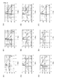
- (A1), (A2) and (A3) in Fig. 6 represent examples in which the output impedance is changed while respective capacitances of the capacitors C1 and C2, respective inductances of the inductors L1 and L2, and the coupling coefficient M between the two LC parallel resonators are all held constant.
- (C1), (C2) and (C3) in Fig. 6 represent examples in which the output impedance is changed while the coupling coefficient M between the two LC parallel resonators is set to a value differing from that set in (A1), (A2) and (A3).
- the impedance matching can be established to some extent by adjusting the coupling coefficient M as described above. As plotted in (C2) of Fig. 6 , however, the characteristic of the reflection loss RL is not improved depending on a value of an imaginary portion of the output impedance Zout.
- the impedance conversion between the input and the output is performed by properly determining the impedance of the LC parallel resonator.
- the characteristic of the reflection loss RL can be greatly improved by determining the impedance of the output-side resonator depending on a ratio of the capacitor C2 to the inductor L2. Accordingly, the multilayer bandpass filter having the impedance conversion function, which is more superior in the impedance matching characteristic, can be constructed by making the above-described impedance setting of the resonator in addition to the known setting of the coupling coefficient between the resonators.
- a multilayer bandpass filter according to a second embodiment will be described below with reference to Figs. 7 to 9 . While the first embodiment has been described in connection with the multilayer bandpass filter which performs the unbalanced inputting/outputting by using two LC parallel resonators, the second embodiment employs three LC parallel resonators to perform not only the above-described impedance conversion, but also balance-unbalance conversion.
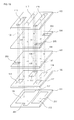
- Fig. 7 is an exploded perspective view of the multilayer bandpass filter according to the second embodiment
- Fig. 8 is a perspective view illustrating an outer appearance of the multilayer bandpass filter.
- the multilayer bandpass filter according to the second embodiment is constructed by layering a plurality of dielectric layers 101 to 105 on which predetermined electrode patterns are formed.
- a first common electrode 109 and a second common electrode 110 are formed on the dielectric layer 101, and capacitor electrodes 111, 112, 113 and 114 are formed on the dielectric layer 102.
- An input/output terminal lead-out electrode 203 is formed on the dielectric layer 103, input/output terminal lead-out electrodes 205 and 206 are formed on the dielectric layer 104, and line electrodes 116, 117 and 118 are formed on the dielectric layer 105.
- via electrodes 131 to 136 are formed to establish conduction in the layering direction between the individual electrode patterns formed on the plural dielectric layers.
- the via electrode 131 is conducted at one end thereof to the capacitor electrode 111 and at the other end thereof to one end of the line electrode 116. Also, the via electrode 131 is conducted at a predetermined position thereof to the input/output terminal lead-out electrode 203.
- the via electrode 132 is conducted at one end thereof to the other end of the line electrode 116 and at the other end thereof to the common electrode 109.
- the via electrode 133 is conducted at one end thereof to the common electrode 109 and at the other end thereof to one end of the line electrode 117.
- the via electrode 134 is conducted at one end thereof to the other end of the line electrode 117 and at the other end thereof to the capacitor electrode 112.
- the via electrode 135 is conducted at one end thereof to one end of the line electrode 118 and at the other end thereof to the capacitor electrode 113. Also, the via electrode 135 is conducted at a predetermined position thereof to the input/output terminal lead-out electrode 205.
- the via electrode 136 is conducted at one end thereof to the other end of the line electrode 118 and at the other end thereof to the capacitor electrode 114. Also, the via electrode 136 is conducted at a predetermined position thereof to the input/output terminal lead-out electrode 206.
- ground terminal lead-out electrodes 201 and 202 are led out from the common electrode 109.
- a first loop is formed by the via electrodes 131 and 132 and the line electrode 116 so as to extend in the layering direction of the dielectric layers.
- a second loop is formed by the via electrodes 133 and 134 and the line electrode 117 so as to extend in the layering direction of the dielectric layers.
- a third loop is formed by the via electrodes 135 and 136 and the line electrode 118 so as to extend in the layering direction of the dielectric layers.
- the loop surfaces are at least partly overlapped such that the first, second and third loops are magnetically coupled to each other.
- respective line lengths of the line electrodes 116, 117 and 118 differ from each other in order to develop a conversion action between the input impedance and the output impedance. Still further, balance-unbalance conversion is performed as described later.
- an unbalanced input/output terminal 23 is disposed on one of two opposite side surfaces (end surfaces) among four side surfaces of the laminate, and balanced input/output terminals 25 and 26 are disposed on the other of the two opposite side surfaces.
- Ground terminals 21 and 22 are disposed on the remaining two side surfaces of the laminate.
- a multilayer bandpass filter 12 is thereby constructed.
- Fig. 9 is an equivalent circuit diagram of the multilayer bandpass filter illustrated in Figs. 7 and 8 .
- an inductor L1 represents, in a symbolic form, the inductance component generated by an inductor electrode that is constituted by the via electrodes 131 and 132 and the line electrode 116, which are illustrated in Fig. 7 .
- an inductor L2 represents, in a symbolic form, the inductance component generated by an inductor electrode that is constituted by the via electrodes 133 and 134 and the line electrode 117.
- An inductor L3 represents, in a symbolic form, the inductance component generated by an inductor electrode that is constituted by the via electrodes 135 and 136 and the line electrode 118.
- a capacitor C1 represents, in a symbolic form, the capacitance generated between the capacitor electrode 111 and the first common electrode 109.
- a capacitor C2 represents, in a symbolic form, the capacitance generated between the capacitor electrode 112 and the first common electrode 109.
- Capacitors C3 and C4 represent, in a symbolic form, the capacitances generated between the capacitor electrodes 113, 114 and the second common electrode 110, respectively.
- a capacitor C12 represents, in a symbolic form, the stray capacitance generated between the via electrodes 131, 132 and the via electrodes 133, 134 and between the line electrodes 116 and 117.
- a capacitor C23 represents, in a symbolic form, the stray capacitance generated between the via electrodes 133, 134 and the via electrodes 135, 136 and between the line electrodes 117 and 118.
- a first LC parallel resonator is constituted by the inductor L1 and the capacitor C1, which are illustrated in Fig. 9
- a second LC parallel resonator is constituted by the inductor L3 and the capacitors C3 and C4.
- the inductor L2 and the capacitor C2 constitute a middle LC parallel resonator that is present between the first LC parallel resonator and the second LC parallel resonator.
- the first LC parallel resonator and the middle LC parallel resonator are magnetically coupled to each other as indicated by M1, whereas the second LC parallel resonator and the middle LC parallel resonator are magnetically coupled to each other as indicated by M2.
- electrode widths of the line electrodes 116, 117 and 118 are set substantially constant in the example illustrated in Fig. 7 , those electrode widths may be set so as to gradually change from the line electrode 116 of the first LC parallel resonator to the line electrode 118 of the second LC parallel resonator. Since such setting enables the inductance components of the respective inductor electrodes to be gradually changed, the impedance change between the adjacent LC parallel resonators is made gentler and the reflection loss can be further reduced.
- the impedance as viewed from the input/output terminal of the first LC parallel resonator can be appropriately determined by leading out the unbalanced input/output terminal lead-out electrode 203 from an intermediate point of the inductor electrode which forms the loop starting from the junction between the via electrode 131 and the capacitor electrode 111, by leading out the balanced input/output terminal lead-out electrode 205 from an intermediate point of the inductor electrode which forms the loop starting from the junction between the via electrode 135 and the capacitor electrode 113, and by leading out the balanced input/output terminal lead-out electrode 206 from an intermediate point of the inductor electrode which forms the loop ending at the junction between the via electrode 136 and the capacitor electrode 114.
- the multilayer bandpass filter can be constructed which can perform the impedance conversion between the input and the output, and which has the unbalance-balance conversion function as well.
- a multilayer bandpass filter according to a third embodiment will be described below with reference to Figs. 10 to 12 .
- the third embodiment employs the three LC parallel resonators to perform both the impedance conversion and the unbalance-balance conversion function which have been described above, and further includes a power supply terminal for DC feed (hereinafter referred to as a "DC feed terminal").
- Fig. 10 is an exploded perspective view of the multilayer bandpass filter according to the third embodiment
- Fig. 11 is a perspective view illustrating an outer appearance of the multilayer bandpass filter.
- a center of a line electrode 118 and a second common electrode 110 are connected to each other through a via electrode 137, and a DC feed terminal lead-out electrode 207 is formed to be led out from the common electrode 110.
- a DC feed terminal lead-out electrode 207 is formed to be led out from the common electrode 110.
- an unbalanced input/output terminal 23 is disposed on one of two opposite side surfaces (end surfaces) among four side surfaces of a laminate, and balanced input/output terminals 25 and 26 and a DC feed terminal 27 are disposed on the other of the two opposite side surfaces.
- Ground terminals 21 and 22 are disposed on the remaining two side surfaces of the laminate.
- a multilayer bandpass filter 13 is thereby constructed.
- Fig. 12 is an equivalent circuit diagram of the multilayer bandpass filter illustrated in Figs. 10 and 11 .
- the circuit illustrated in Fig. 12 differs from the circuit illustrated in Fig. 9 in that a center of an inductor L3 is connected to a junction between capacitors C3 and C4, and that the DC feed terminal 27 is led out from the junction between the capacitors C3 and C4.
- the multilayer bandpass filter can be constructed which can perform the impedance conversion between the input and the output, and which has the unbalance-balance conversion function as well.
- a bias voltage can be applied from the DC feed terminal 27 to a differential amplification circuit (IC chip) that is connected to the balanced input/output terminals 25 and 26.
- a multilayer bandpass filter according to a fourth embodiment will be described with reference to Figs. 13 to 15 .
- the fourth embodiment employs the three LC parallel resonators to perform both the impedance conversion and unbalance-balance conversion function, and further includes a capacitor between a DC feed terminal and a ground.
- Fig. 13 is an exploded perspective view of the multilayer bandpass filter according to the fourth embodiment
- Fig. 14 is a perspective view illustrating an outer appearance of the multilayer bandpass filter.
- a dielectric layer 100 is disposed with a capacitor electrode 115 and a DC feed terminal lead-out electrode 208 formed on the dielectric layer 100, and the capacitor electrode 115 and the second common electrode 110 are conducted to each other through a via electrode.
- an unbalanced input/output terminal 23 and a DC feed terminal 28 are disposed on one of two opposite side surfaces (end surfaces) among four side surfaces of a laminate, and balanced input/output terminals 25 and 26 are disposed on the other of the two opposite side surfaces.
- Ground terminals 21 and 22 are disposed on the remaining two side surfaces of the laminate.
- a multilayer bandpass filter 14 is thereby constructed.
- a capacitor C5 represents the capacitance generated between the capacitor electrode 115 and the first common electrode 109, which are illustrated in Fig. 13 .
- a line electrode 116 is formed on a dielectric layer 105a
- a line electrode 117 is formed on a dielectric layer 105b
- a line electrode 118 is formed on a dielectric layer 105c.
- the line electrodes serving as parts of respective inductor electrodes of three LC parallel resonators are formed on different dielectric layers.
- the other construction in a fifth embodiment is similar to that in the fourth embodiment.
- a loop area of the inductor electrode which is formed by the via electrodes and the line electrode of each LC parallel resonator, can be determined as appropriate, a desired impedance can be set at a higher degree of freedom.
- the loop area can be arbitrarily set just by forming the line electrodes on different (changed) ones of the dielectric layers and changing the number and the thicknesses of dielectric layers which are additionally inserted between the above-described dielectric layers, while respective patterns of the line electrodes 116, 117 and 118 are kept the same.
- dielectric sheets can be used in common and the manufacturing cost can be greatly cut with no necessity of forming a different electrode pattern for each of filters having different characteristics.
- Fig. 17 is an exploded perspective view of a multilayer bandpass filter according to a sixth embodiment.
- the line electrode 117 is bent in its part such that the part of the line electrode 117 comes closer to the adjacent line electrode 118.
- Such a structure can increase the coupling degree between the LC parallel resonator including the inductor electrode, which is formed by the via electrodes 133 and 134 and the line electrode 117, and the LC parallel resonator including the inductor electrode, which is formed by the via electrodes 135 and 136 and the line electrode 118.
- the reflection loss can be reduced by determining not only the impedance of each resonator, but also the coupling coefficient between the adjacent resonators as described above.
- first and second common electrodes may be formed on different ones of the above-described dielectric layers such that the inductances of the inductor electrodes are set to predetermined values.
Landscapes
- Physics & Mathematics (AREA)
- Electromagnetism (AREA)
- Engineering & Computer Science (AREA)
- Power Engineering (AREA)
- Control Of Motors That Do Not Use Commutators (AREA)
- Filters And Equalizers (AREA)
Abstract
Description
- The present invention relates to a multilayer bandpass filter in which a plurality of dielectric layers and a plurality of electrode layers are multilayered.
- Hitherto, a high-frequency bandpass filter suitable for reduction in size and cost has been constructed by providing a plurality of LC resonators within a laminate in which dielectric layers and electrode layers are multilayered.
That type of multilayer bandpass filter is disclosed inPatent Literature 1. - The construction of the multilayer bandpass filter disclosed in
Patent Literature 1 will be described with reference toFig. 1 .
Fig. 1 is a circuit diagram of the multilayer bandpass filter disclosed inPatent Literature 1. Themultilayer bandpass filter 1 includes anunbalanced input terminal 2,balanced output terminals bandpass filter section 4 disposed between theunbalanced input terminal 2 and thebalanced output terminals bandpass filter section 4 includes threeresonators 40, which are each constituted as a 1/2-wavelength resonator 41 with both ends being open and which are arranged side by side. Among the threeresonators 40, oneresonator 40 arranged at a position closest to theunbalanced input terminal 2 serves as an input resonator 40I. Theunbalanced input terminal 2 is directly connected to the input resonator 40I. Anotherresonator 40 arranged at a position closest to thebalanced output terminals wavelength resonator 41A for balanced output. Thebalanced output terminals wavelength resonator 41A for balanced output. The input resonator 40I and amiddle resonator 40M are electromagnetically coupled to each other, and themiddle resonator 40M and the 1/2-wavelength resonator 41A for balanced output are also electromagnetically coupled to each other. Further, a capacitor C is disposed between each of the open ends of the threeresonators 40 and a ground. -
- Patent Literature 1: Japanese Unexamined Patent Application Publication No.
2005-45447 - In the multilayer bandpass filter disclosed in
Patent Literature 1, the λ/2 resonators each having both the open ends are arranged on the same substrate surface for coupling between the resonators so as to provide filter characteristics. - In the multilayer bandpass filter disclosed in
Patent Literature 1, however, a degree of coupling between the resonators can be controlled for proper adjustment only by setting the spacing between the resonators in the substrate surface. When strong coupling is to be obtained, the spacing between the resonators needs to be narrowed. Also, the coupling degree varies due to variation in formation of electrodes, etc. This gives rise to a problem that desired filter characteristics are not obtained. - Further, because the shape of the resonator is determined depending on the frequency of the passband, there has also been a limitation in reducing the size of the filter.
- In many cases, the balanced terminal side is connected to, e.g., IC input and output signals in the balanced type. In such a case, impedance needs to be converted between the unbalanced terminal and the balanced terminals. With the structure disclosed in
Patent Literature 1, however, it is not easy to perform setting and adjustment for proper impedance conversion between both the types of terminals. - Accordingly, an object of the present invention is to solve the above-mentioned problems and to provide a multilayer bandpass filter that can suppress variation in filter characteristics caused by variation in electrode formation, etc., can easily reduce its size, and can carry out predetermined impedance conversion between an input and an output.
- To solve the above-mentioned problems, a multilayer bandpass filter according to the present invention is constructed as follows.
- (1) In a multilayer bandpass filter including, as an elementary body, a laminate formed by a plurality of dielectric layers and a plurality of electrode layers each including at least one type of a capacitor electrode and/or an inductor electrode,
a plurality of two or more LC parallel resonators are each constituted by the capacitor electrode and the inductor electrode, adjacent two of the LC parallel resonators being coupled to each other,
the multilayer bandpass filter further includes an input/output terminal lead-out electrode to which is coupled a first LC parallel resonator arranged at one end of the laminate among the plurality of LC parallel resonators and which serves as an input portion of the multilayer bandpass filter, and an input/output terminal lead-out electrode to which is coupled a second LC parallel resonator arranged at the other end of the laminate and which serves as an output portion of the multilayer bandpass filter,
the inductor electrodes of the plurality of LC parallel resonators are constituted by line electrodes which are formed on a surface of and/or within the laminate side by side in a direction perpendicular to a layering direction of the laminate, and by via electrodes which are conducted to at least one ends of the line electrodes and which are extended in the layering direction of the laminate,
the inductor electrodes are formed such that surfaces of loops starting from junctions between the via electrodes and the capacitor electrodes and including the line electrodes, respectively, are arrayed side by side in the direction perpendicular to the layering direction of the laminate, the loop surfaces overlapping with each other at least partly when the loop surfaces formed by the inductor electrodes of the LC parallel resonators coupled to each other are viewed in the direction in which the line electrodes are arrayed side by side, and
line lengths of the line electrodes are gradually changed from the first LC parallel resonator side toward the second LC parallel resonator side such that impedance conversion is performed between the input portion and the output portion. -
- (2) As the occasion requires, line widths of the line electrodes are gradually changed from the first LC parallel resonator side toward the second LC parallel resonator side.
With that feature, the impedance conversion between the input and the output can be realized over a wider range. -
- (3) A part of at least one of the line electrodes in a longitudinal direction thereof is positioned closer to another adjacent line electrode.
With that feature, a degree of freedom in coupling between the adjacent resonators can be increased. -
- (4) As the occasion requires, at least one of the line electrodes is formed on the dielectric layer differing from the dielectric layer on which the other one or more line electrodes are formed.
With that feature, an area of the loop surface can be easily changed without changing a pattern formed on the dielectric layer. -
- (5) The capacitor electrode includes at least first and second common electrodes, the first common electrode being conducted to a ground electrode, the second common electrode being not conducted to the ground electrode, the input/output terminal lead-out electrode to which is coupled the first LC parallel resonator is an unbalanced input/output terminal lead-out electrode, and the input/output terminal lead-out electrode to which is coupled the second LC parallel resonator is a pair of balanced input/output terminal lead-out electrodes.
With that feature, the balance-unbalance conversion function can also be provided. -
- (6) The balanced input/output terminal lead-out electrodes are arranged respectively at substantially equal distances from a center of the line electrode of the second LC parallel resonator in a longitudinal direction thereof.
With that feature, a balance characteristic is improved. -
- (7) The unbalanced input/output terminal lead-out electrode and the balanced input/output terminal lead-out electrodes are formed respectively on different ones of the dielectric layers.
With that feature, an input impedance and an output impedance can be set at a high degree of freedom. -
- (8) The first and second common electrodes are formed respectively on different ones of the dielectric layers.
With that feature, an area of the loop surface can be easily changed without changing a pattern formed on the dielectric layer. -
- (9) The capacitor electrode includes at least the first and second common electrodes, the first common electrode being conducted to the ground electrode, the second common electrode being not conducted to the ground electrode, and the multilayer bandpass filter further includes a via electrode for conducting a central portion of the line electrode of the second LC parallel resonator in a longitudinal direction thereof and the second common electrode to each other.
-
- (10) The power supply terminal is formed to be led out from the second common electrode.
With that feature, the power supply terminal for DC feed can be easily provided without using a special dielectric layer. -
- (11) Input/output terminals, which are connected to the unbalanced input/output terminal lead-out electrode and the balanced input/output terminal lead-out electrodes, and a ground terminal, which is connected to the ground electrode, are arranged on side surfaces of the laminate.
With that feature, a multilayer bandpass filter can be constructed which can be surface-mounted and which has the balance-unbalance conversion function. -
- (12) The dielectric layer is made of a low-temperature sintered ceramic.
With that feature, capacitance per unit area can be increased and the entire size of the multilayer bandpass filter can be reduced. -
- (13) The dielectric layer is made of a resin.
That feature enables the dielectric layer forming the laminate to have a lower dielectric constant and makes the multilayer bandpass filter adaptable for higher frequency. Advantageous Effects of Invention - According to the present invention, the multilayer bandpass filter can be constructed to be capable of suppressing variation in filter characteristics caused by variation in electrode formation, etc., easily reducing its size, and carrying out predetermined impedance conversion between an input and an output.
-
- [
Fig. 1] Fig. 1 is a circuit diagram of a multilayer bandpass filter disclosed inPatent Literature 1. - [
Fig. 2] Fig. 2 is an exploded perspective view of a multilayer bandpass filter according to a first embodiment. - [
Fig. 3] Fig. 3 is a perspective view illustrating an outer appearance of the multilayer bandpass filter according to the first embodiment. - [
Fig. 4] Fig. 4 is an equivalent circuit diagram of the multilayer bandpass filter illustrated inFigs. 2 and3 . - [
Fig. 5] Fig. 5 is a graph plotting characteristics of an insertion loss IL and a reflection loss RL as viewed from one unbalanced input/output terminal when an input impedance and an output impedance are each set to 50 Ω. - [
Fig. 6 ] (A1), (A2) and (A3) inFig. 6 represent examples in which the output impedance is changed while respective capacitances of capacitors C1 and C2 of LC parallel resonators, respective inductances of inductors L1 and L2 thereof, and a coupling coefficient M therebetween are all held constant. (C1), (C2) and (C3) represent examples in which the output impedance is changed while the coupling coefficient M is set to a value differing from that set in (A1), (A2) and (A3). (B1), (B2) and (B3) represent examples in which the output impedance is changed while the capacitance of the capacitor C2 and the inductance of the inductor L2 of the LC parallel resonator on the output side are set to values differing from those set in (A1), (A2) and (A3) . - [
Fig. 7] Fig. 7 is an exploded perspective view of a multilayer bandpass filter according to a second embodiment. - [
Fig. 8] Fig. 8 is a perspective view illustrating an outer appearance of the multilayer bandpass filter according to the second embodiment. - [
Fig. 9] Fig. 9 is an equivalent circuit diagram of the multilayer bandpass filter according to the second embodiment. - [
Fig. 10] Fig. 10 is an exploded perspective view of a multilayer bandpass filter according to a third embodiment. - [
Fig. 11] Fig. 11 is a perspective view illustrating an outer appearance of the multilayer bandpass filter according to the third embodiment. - [
Fig. 12] Fig. 12 is an equivalent circuit diagram of the multilayer bandpass filter according to the third embodiment. - [
Fig. 13] Fig. 13 is an exploded perspective view of a multilayer bandpass filter according to a fourth embodiment. - [
Fig. 14] Fig. 14 is a perspective view illustrating an outer appearance of the multilayer bandpass filter according to the fourth embodiment. - [
Fig. 15] Fig. 15 is an equivalent circuit diagram of the multilayer bandpass filter according to the fourth embodiment. - [
Fig. 16] Fig. 16 is an exploded perspective view of a multilayer bandpass filter according to a fifth embodiment. - [
Fig. 17] Fig. 17 is an exploded perspective view of a multilayer bandpass filter according to a sixth embodiment. - A multilayer bandpass filter according to a first embodiment will be described below with reference to
Figs. 2 to 6 .
Fig. 2 is an exploded perspective view of the multilayer bandpass filter according to the first embodiment, andFig. 3 is a perspective view illustrating an outer appearance of the multilayer bandpass filter. - As illustrated in
Fig. 2 , the multilayer bandpass filter according to the first embodiment is constructed by layering a plurality ofdielectric layers 101 to 105 on which predetermined electrode patterns are formed. - A
common electrode 109 is formed on thedielectric layer 101, andcapacitor electrodes dielectric layer 102. An input/output terminal lead-outelectrode 203 is formed on thedielectric layer 103, an input/output terminal lead-outelectrode 204 is formed on thedielectric layer 104, andline electrodes dielectric layer 105. Further, viaelectrodes 131 to 134 are formed to establish conduction in the layering direction between the individual electrode patterns formed on the plural dielectric layers. - The input/output terminal lead-out
electrodes - The via
electrode 131 is conducted at one end thereof to thecapacitor electrode 111 and at the other end thereof to one end of theline electrode 116. Also, the viaelectrode 131 is conducted at a predetermined position thereof to the input/output terminal lead-outelectrode 203. - The via
electrode 132 is conducted at one end thereof to the other end of theline electrode 116 and at the other end thereof to thecommon electrode 109.
The viaelectrode 133 is conducted at one end thereof to thecommon electrode 109 and at the other end thereof to one end of theline electrode 117. - The via
electrode 134 is conducted at one end thereof to the other end of theline electrode 117 and at the other end thereof to thecapacitor electrode 112. Also, the viaelectrode 134 is conducted at a predetermined position thereof to the input/output terminal lead-outelectrode 204. - Further, two ground terminal lead-out
electrodes common electrode 109. - As illustrated in
Fig. 2 , starting from a junction between the viaelectrode 131 and thecapacitor electrode 111, a first loop is formed by the viaelectrodes line electrode 116 so as to extend in the layering direction of the dielectric layers. Similarly, starting from a junction between the viaelectrode 134 and thecapacitor electrode 112, a second loop is formed by the viaelectrodes line electrode 117 so as to extend in the layering direction of the dielectric layers. - Thus, looking at respective surfaces of loops formed by inductor electrodes of LC parallel resonators in a direction in which the inductor electrodes are arrayed side by side, i.e., as viewed in a direction not only perpendicular to the longitudinal direction of the line electrodes, but also perpendicular to the layering direction of the dielectric layers, the loop surfaces are at least partly overlapped such that the first and second loops are magnetically coupled to each other. Further, respective line lengths of the
line electrodes - In addition to constructing a laminate of the
dielectric layers 101 to 105 on which the various electrode patterns are formed, as illustrated inFig. 3 , unbalanced input/output terminals ground terminals multilayer bandpass filter 11 is thereby constructed. - Each of dielectric portions of the
dielectric layers 101 to 105 has a specific dielectric constant in the range of 6 to 80. In particular, thedielectric layer 102 generating capacitance has a specific dielectric constant of not smaller than 20. The dielectric layers are each formed by using a low-temperature co-fired ceramic (LTCC) that is made of at least one selected from among titanium oxide, barium oxide, alumina, etc., and a glassy component. As an alternative, each dielectric layer is formed by using a resin, such as a liquid crystal polymer (LCP) or polyimide.
The above-mentioned materials of the dielectric layers are similarly used in other embodiments described below. -
Fig. 4 is an equivalent circuit diagram of the multilayer bandpass filter illustrated inFigs. 2 and3 . InFig. 4 , an inductor L1 represents, in a symbolic form, the inductance component generated by an inductor electrode that is constituted by the viaelectrodes line electrode 116, which are illustrated inFig. 2 . - Similarly, an inductor L2 represents, in a symbolic form, the inductance component generated by an inductor electrode that is constituted by the via
electrodes line electrode 117. - Further, a capacitor C1 represents, in a symbolic form, the capacitance generated between the
capacitor electrode 111 and thecommon electrode 109. Similarly, a capacitor C2 represents, in a symbolic form, the capacitance generated between thecapacitor electrode 112 and thecommon electrode 109. - A capacitor C12 represents, in a symbolic form, the stray capacitance generated between the via
electrodes electrodes line electrodes - A first LC parallel resonator is constituted by the inductor L1 and the capacitor C1, which are illustrated in
Fig. 4 , and a second LC parallel resonator is constituted by the inductor L2 and the capacitor C2. - Operation effects of the above-described impedance conversion and a design method for the same will be described below with reference to
Figs. 5 and6 .
Fig. 5 plots characteristics of an insertion loss IL and a reflection loss RL as viewed from one unbalanced input/output terminal (i.e., the input-side terminal) when the capacitance of each of the capacitors C1 and C2 illustrated inFig. 4 is set to 8 pF, the inductance of each of the inductors L1 and L2 is set to 0.5 nH, a coupling coefficient M between the two LC parallel resonators is set to 0.1, and the input impedance and the output impedance are each set to 50 Ω. Be it noted that, when the input impedance and the output impedance are equal to each other as mentioned above, a resulting circuit is symmetrical between the input and the output unlike the example illustrated inFig. 2 . - (A1), (A2) and (A3) in
Fig. 6 represent examples in which the output impedance is changed while respective capacitances of the capacitors C1 and C2, respective inductances of the inductors L1 and L2, and the coupling coefficient M between the two LC parallel resonators are all held constant. Also, (C1), (C2) and (C3) inFig. 6 represent examples in which the output impedance is changed while the coupling coefficient M between the two LC parallel resonators is set to a value differing from that set in (A1), (A2) and (A3). Further, (B1), (B2) and (B3) inFig. 6 represent examples in which the output impedance is changed while the capacitance of the capacitor C2 and the inductance of the inductor L2 of the LC parallel resonator on the output side are set to values differing from those set in (A1), (A2) and (A3). In all the graphs ofFig. 6 , the vertical axis represents a loss [dB]. - In (A1), (B1) and (C1), the input impedance Zin = 50 Ω and the output impedance Zout = 100 Ω are set. Further, (A2), (B2) and (C2) represent changes of the insertion loss IL and the reflection loss RL in the case of Zin = 50 Ω and Zout = 50 - J50 Ω (1/ωC (reactance) = 50 Ω). (A3), (B3) and (C3) represent those changes in the case of Zin = 50 Ω and Zout = 100 - J50Ω (1/ωC (reactance) = 50 Ω).
- As is apparent from comparison between
Fig. 5 and (A1) to (A3) inFig. 6 , the reflection loss RL increases with a deviation of the impedance of a circuit connected to the output of the filter, which has been designed with Zin = 50 Ω and Zout = 50 Ω. - Hitherto, the coupling coefficient M between the LC parallel resonators has been adjusted to establish impedance matching in agreement with the impedance required for the circuit which is connected to an output stage of the filter. (C1) to (C3) in
Fig. 6 represent the examples in each of which M = 0.12 is set. - The impedance matching can be established to some extent by adjusting the coupling coefficient M as described above. As plotted in (C2) of
Fig. 6 , however, the characteristic of the reflection loss RL is not improved depending on a value of an imaginary portion of the output impedance Zout. - On the other hand, in the present invention, the impedance conversion between the input and the output is performed by properly determining the impedance of the LC parallel resonator. (B1) to (B3) in
Fig. 6 represent the examples in which the capacitance of the capacitor C2 of the LC parallel resonator on the output side is set to 10 pF, the inductance of the inductor L2 thereof is set to 0.4 nH, and the coupling coefficient M is held fixed at M = 0.1. - As is apparent from comparing (A2), (B2) and (C2) in
Fig. 6 , the characteristic of the reflection loss RL can be greatly improved by determining the impedance of the output-side resonator depending on a ratio of the capacitor C2 to the inductor L2. Accordingly, the multilayer bandpass filter having the impedance conversion function, which is more superior in the impedance matching characteristic, can be constructed by making the above-described impedance setting of the resonator in addition to the known setting of the coupling coefficient between the resonators. - A multilayer bandpass filter according to a second embodiment will be described below with reference to
Figs. 7 to 9 .
While the first embodiment has been described in connection with the multilayer bandpass filter which performs the unbalanced inputting/outputting by using two LC parallel resonators, the second embodiment employs three LC parallel resonators to perform not only the above-described impedance conversion, but also balance-unbalance conversion. -
Fig. 7 is an exploded perspective view of the multilayer bandpass filter according to the second embodiment, andFig. 8 is a perspective view illustrating an outer appearance of the multilayer bandpass filter.
As illustrated inFig. 7 , the multilayer bandpass filter according to the second embodiment is constructed by layering a plurality ofdielectric layers 101 to 105 on which predetermined electrode patterns are formed. - A first
common electrode 109 and a secondcommon electrode 110 are formed on thedielectric layer 101, andcapacitor electrodes dielectric layer 102. An input/output terminal lead-outelectrode 203 is formed on thedielectric layer 103, input/output terminal lead-outelectrodes dielectric layer 104, andline electrodes dielectric layer 105. Further, viaelectrodes 131 to 136 are formed to establish conduction in the layering direction between the individual electrode patterns formed on the plural dielectric layers. - The via
electrode 131 is conducted at one end thereof to thecapacitor electrode 111 and at the other end thereof to one end of theline electrode 116. Also, the viaelectrode 131 is conducted at a predetermined position thereof to the input/output terminal lead-outelectrode 203. - The via
electrode 132 is conducted at one end thereof to the other end of theline electrode 116 and at the other end thereof to thecommon electrode 109.
The viaelectrode 133 is conducted at one end thereof to thecommon electrode 109 and at the other end thereof to one end of theline electrode 117. - The via
electrode 134 is conducted at one end thereof to the other end of theline electrode 117 and at the other end thereof to thecapacitor electrode 112. - The via
electrode 135 is conducted at one end thereof to one end of theline electrode 118 and at the other end thereof to thecapacitor electrode 113. Also, the viaelectrode 135 is conducted at a predetermined position thereof to the input/output terminal lead-outelectrode 205. - The via
electrode 136 is conducted at one end thereof to the other end of theline electrode 118 and at the other end thereof to thecapacitor electrode 114. Also, the viaelectrode 136 is conducted at a predetermined position thereof to the input/output terminal lead-outelectrode 206. - Further, two ground terminal lead-out
electrodes common electrode 109. - As illustrated in
Fig. 7 , starting from a junction between the viaelectrode 131 and thecapacitor electrode 111, a first loop is formed by the viaelectrodes line electrode 116 so as to extend in the layering direction of the dielectric layers. Similarly, starting from a junction between the viaelectrode 134 and thecapacitor electrode 112, a second loop is formed by the viaelectrodes line electrode 117 so as to extend in the layering direction of the dielectric layers. Further, starting from a junction between the viaelectrode 135 and thecapacitor electrode 113, a third loop is formed by the viaelectrodes line electrode 118 so as to extend in the layering direction of the dielectric layers. - Thus, looking at respective surfaces of loops formed by inductor electrodes of LC parallel resonators in a direction in which the inductor electrodes are arrayed side by side, i.e., as viewed in a direction not only perpendicular to the longitudinal direction of the line electrodes, but also perpendicular to the layering direction of the dielectric layers, the loop surfaces are at least partly overlapped such that the first, second and third loops are magnetically coupled to each other. Further, respective line lengths of the
line electrodes - In addition to constructing a laminate of the
dielectric layers 101 to 105 on which the various electrode patterns are formed, as illustrated inFig. 8 , an unbalanced input/output terminal 23 is disposed on one of two opposite side surfaces (end surfaces) among four side surfaces of the laminate, and balanced input/output terminals Ground terminals multilayer bandpass filter 12 is thereby constructed. -
Fig. 9 is an equivalent circuit diagram of the multilayer bandpass filter illustrated inFigs. 7 and8 . InFig. 9 , an inductor L1 represents, in a symbolic form, the inductance component generated by an inductor electrode that is constituted by the viaelectrodes line electrode 116, which are illustrated inFig. 7 . Similarly, an inductor L2 represents, in a symbolic form, the inductance component generated by an inductor electrode that is constituted by the viaelectrodes line electrode 117. - An inductor L3 represents, in a symbolic form, the inductance component generated by an inductor electrode that is constituted by the via
electrodes line electrode 118. - Further, a capacitor C1 represents, in a symbolic form, the capacitance generated between the
capacitor electrode 111 and the firstcommon electrode 109. Similarly, a capacitor C2 represents, in a symbolic form, the capacitance generated between thecapacitor electrode 112 and the firstcommon electrode 109. - Capacitors C3 and C4 represent, in a symbolic form, the capacitances generated between the
capacitor electrodes common electrode 110, respectively. - A capacitor C12 represents, in a symbolic form, the stray capacitance generated between the via
electrodes electrodes line electrodes electrodes electrodes line electrodes - A first LC parallel resonator is constituted by the inductor L1 and the capacitor C1, which are illustrated in
Fig. 9 , and a second LC parallel resonator is constituted by the inductor L3 and the capacitors C3 and C4. The inductor L2 and the capacitor C2 constitute a middle LC parallel resonator that is present between the first LC parallel resonator and the second LC parallel resonator. - The first LC parallel resonator and the middle LC parallel resonator are magnetically coupled to each other as indicated by M1, whereas the second LC parallel resonator and the middle LC parallel resonator are magnetically coupled to each other as indicated by M2.
- Thus, by setting respective line lengths of the
line electrodes - While electrode widths of the
line electrodes Fig. 7 , those electrode widths may be set so as to gradually change from theline electrode 116 of the first LC parallel resonator to theline electrode 118 of the second LC parallel resonator. Since such setting enables the inductance components of the respective inductor electrodes to be gradually changed, the impedance change between the adjacent LC parallel resonators is made gentler and the reflection loss can be further reduced. - Further, the impedance as viewed from the input/output terminal of the first LC parallel resonator can be appropriately determined by leading out the unbalanced input/output terminal lead-out
electrode 203 from an intermediate point of the inductor electrode which forms the loop starting from the junction between the viaelectrode 131 and thecapacitor electrode 111, by leading out the balanced input/output terminal lead-outelectrode 205 from an intermediate point of the inductor electrode which forms the loop starting from the junction between the viaelectrode 135 and thecapacitor electrode 113, and by leading out the balanced input/output terminal lead-outelectrode 206 from an intermediate point of the inductor electrode which forms the loop ending at the junction between the viaelectrode 136 and thecapacitor electrode 114. - Thus, the multilayer bandpass filter can be constructed which can perform the impedance conversion between the input and the output, and which has the unbalance-balance conversion function as well.
- A multilayer bandpass filter according to a third embodiment will be described below with reference to
Figs. 10 to 12 .
The third embodiment employs the three LC parallel resonators to perform both the impedance conversion and the unbalance-balance conversion function which have been described above, and further includes a power supply terminal for DC feed (hereinafter referred to as a "DC feed terminal"). -
Fig. 10 is an exploded perspective view of the multilayer bandpass filter according to the third embodiment, andFig. 11 is a perspective view illustrating an outer appearance of the multilayer bandpass filter.
In the multilayer bandpass filter according to the third embodiment, unlike the structure of the multilayer bandpass filter according to the second embodiment illustrated inFig. 7 , a center of aline electrode 118 and a secondcommon electrode 110 are connected to each other through a viaelectrode 137, and a DC feed terminal lead-outelectrode 207 is formed to be led out from thecommon electrode 110. As illustrated inFig. 11 , an unbalanced input/output terminal 23 is disposed on one of two opposite side surfaces (end surfaces) among four side surfaces of a laminate, and balanced input/output terminals DC feed terminal 27 are disposed on the other of the two opposite side surfaces.Ground terminals multilayer bandpass filter 13 is thereby constructed. -
Fig. 12 is an equivalent circuit diagram of the multilayer bandpass filter illustrated inFigs. 10 and11 . The circuit illustrated inFig. 12 differs from the circuit illustrated inFig. 9 in that a center of an inductor L3 is connected to a junction between capacitors C3 and C4, and that theDC feed terminal 27 is led out from the junction between the capacitors C3 and C4. - Thus, the multilayer bandpass filter can be constructed which can perform the impedance conversion between the input and the output, and which has the unbalance-balance conversion function as well. In addition, a bias voltage can be applied from the
DC feed terminal 27 to a differential amplification circuit (IC chip) that is connected to the balanced input/output terminals - A multilayer bandpass filter according to a fourth embodiment will be described with reference to
Figs. 13 to 15 .
The fourth embodiment employs the three LC parallel resonators to perform both the impedance conversion and unbalance-balance conversion function, and further includes a capacitor between a DC feed terminal and a ground. -
Fig. 13 is an exploded perspective view of the multilayer bandpass filter according to the fourth embodiment, andFig. 14 is a perspective view illustrating an outer appearance of the multilayer bandpass filter.
In the fourth embodiment illustrated inFig. 13 , unlike the structure of the multilayer bandpass filter according to the third embodiment illustrated inFig. 10 , adielectric layer 100 is disposed with acapacitor electrode 115 and a DC feed terminal lead-outelectrode 208 formed on thedielectric layer 100, and thecapacitor electrode 115 and the secondcommon electrode 110 are conducted to each other through a via electrode. - As illustrated in
Fig. 14 , an unbalanced input/output terminal 23 and aDC feed terminal 28 are disposed on one of two opposite side surfaces (end surfaces) among four side surfaces of a laminate, and balanced input/output terminals Ground terminals multilayer bandpass filter 14 is thereby constructed. - In
Fig. 15 , a capacitor C5 represents the capacitance generated between thecapacitor electrode 115 and the firstcommon electrode 109, which are illustrated inFig. 13 . - Thus, with the capacitor C5 disposed between the DC feed terminal and the ground, a high-frequency signal can be prevented from being input to the
DC feed terminal 28. - In
Fig. 16 , aline electrode 116 is formed on adielectric layer 105a, aline electrode 117 is formed on adielectric layer 105b, and aline electrode 118 is formed on adielectric layer 105c. Stated another way, the line electrodes serving as parts of respective inductor electrodes of three LC parallel resonators are formed on different dielectric layers. The other construction in a fifth embodiment is similar to that in the fourth embodiment. - With such a construction, since a loop area of the inductor electrode, which is formed by the via electrodes and the line electrode of each LC parallel resonator, can be determined as appropriate, a desired impedance can be set at a higher degree of freedom. Furthermore, the loop area can be arbitrarily set just by forming the line electrodes on different (changed) ones of the dielectric layers and changing the number and the thicknesses of dielectric layers which are additionally inserted between the above-described dielectric layers, while respective patterns of the
line electrodes -
Fig. 17 is an exploded perspective view of a multilayer bandpass filter according to a sixth embodiment. In the sixth embodiment, unlike the second embodiment illustrated inFig. 7 , theline electrode 117 is bent in its part such that the part of theline electrode 117 comes closer to theadjacent line electrode 118. Such a structure can increase the coupling degree between the LC parallel resonator including the inductor electrode, which is formed by the viaelectrodes line electrode 117, and the LC parallel resonator including the inductor electrode, which is formed by the viaelectrodes line electrode 118. - Thus, the reflection loss can be reduced by determining not only the impedance of each resonator, but also the coupling coefficient between the adjacent resonators as described above.
- While the line electrodes constituting parts of the respective inductor electrodes of the plural LC parallel resonators are formed on the surface of the laminate in the above-described embodiments, those inductor electrodes may be all disposed inside the laminate.
- Further, the first and second common electrodes may be formed on different ones of the above-described dielectric layers such that the inductances of the inductor electrodes are set to predetermined values.
-
- 11 to 14 ... multilayer bandpass filters
- 21, 22 ... ground terminals
- 23, 24 ... unbalanced input/output terminals
- 25, 26 ... balanced input/output terminals
- 27, 28 ... DC feed terminals
- 100 to 105 ... dielectric layers
- 109 ... first common electrode (common electrode)
- 110 ... second common electrode
- 111 to 115 ... capacitor electrodes
- 116 to 118 ... line electrodes
- 131 to 137 ... via electrodes
- 201, 202 ... ground terminal lead-out electrodes
- 203, 204 ... unbalanced input/output terminal lead-out electrodes
- 205, 206 ... balanced input/output terminal lead-out electrodes
- 207, 208 ... DC feed terminal lead-out electrodes
Claims (13)
- A multilayer bandpass filter including, as an elementary body, a laminate formed by a plurality of dielectric layers and a plurality of electrode layers each including at least one type of a capacitor electrode and/or an inductor electrode, wherein:a plurality of two or more LC parallel resonators are each constituted by the capacitor electrode and the inductor electrode, adjacent two of the LC parallel resonators being coupled to each other,the multilayer bandpass filter further includes an input/output terminal lead-out electrode to which is coupled a first LC parallel resonator arranged at one end of the laminate among the plurality of LC parallel resonators and which serves as an input portion of the multilayer bandpass filter, and an input/output terminal lead-out electrode to which is coupled a second LC parallel resonator arranged at the other end of the laminate and which serves as an output portion of the multilayer bandpass filter,the inductor electrodes of the plurality of LC parallel resonators are constituted by line electrodes which are formed on a surface of and/or within the laminate side by side in a direction perpendicular to a layering direction of the laminate, and by via electrodes which are conducted to at least one ends of the line electrodes and which are extended in the layering direction of the laminate,the inductor electrodes are respectively formed such that surfaces of loops starting from junctions between the via electrodes and the capacitor electrodes and including the line electrodes are arrayed side by side in the direction perpendicular to the layering direction of the laminate, the loop surfaces overlapping with each other at least partly when the loop surfaces formed by the inductor electrodes of the LC parallel resonators coupled to each other are viewed in the direction in which the line electrodes are arrayed side by side, andline lengths of the line electrodes are gradually changed from the first LC parallel resonator side toward the second LC parallel resonator side such that impedance conversion is performed between the input portion and the output portion.
- The multilayer bandpass filter according to Claim 1, wherein line widths of the line electrodes are gradually changed from the first LC parallel resonator side toward the second LC parallel resonator side.
- The multilayer bandpass filter according to Claim 1 or 2, wherein a part of at least one of the line electrodes in a longitudinal direction thereof is positioned closer to another adjacent line electrode.
- The multilayer bandpass filter according to Claim 1, 2 or 3, wherein at least one of the line electrodes is formed on the dielectric layer differing from the dielectric layer on which the other one or more line electrodes are formed.
- The multilayer bandpass filter according to any one of Claims 1 to 4, wherein the capacitor electrode includes at least first and second common electrodes, the first common electrode being conducted to a ground electrode, the second common electrode being not conducted to the ground electrode, the input/output terminal lead-out electrode to which is coupled the first LC parallel resonator is an unbalanced input/output terminal lead-out electrode, and the input/output terminal lead-out electrode to which is coupled the second LC parallel resonator is a pair of balanced input/output terminal lead-out electrodes.
- The multilayer bandpass filter according to Claim 5, wherein the balanced input/output terminal lead-out electrodes are arranged respectively at substantially equal distances from a center of the line electrode of the second LC parallel resonator in a longitudinal direction thereof.
- The multilayer bandpass filter according to Claim 5 or 6, wherein the unbalanced input/output terminal lead-out electrode and the balanced input/output terminal lead-out electrodes are formed respectively on different ones of the dielectric layers.
- The multilayer bandpass filter according to any one of Claims 5 to 7, wherein the first and second common electrodes are formed respectively on different ones of the dielectric layers.
- The multilayer bandpass filter according to any one of Claims 5 to 8, wherein the capacitor electrode includes at least the first and second common electrodes, the first common electrode being conducted to the ground electrode, the second common electrode being not conducted to the ground electrode, and the multilayer bandpass filter further includes a via electrode for conducting a central portion of the line electrode of the second LC parallel resonator in a longitudinal direction thereof and the second common electrode to each other.
- The multilayer bandpass filter according to Claim 9, wherein a power supply terminal lead-out electrode is formed to be led out from the second common electrode.
- The multilayer bandpass filter according to any one of Claims 5 to 10, wherein input/output terminals, which are connected to the unbalanced input/output terminal lead-out electrode and the balanced input/output terminal lead-out electrodes, and a ground terminal, which is connected to the ground electrode, are arranged on side surfaces of the laminate.
- The multilayer bandpass filter according to any one of Claims 1 to 11, wherein the dielectric layer is made of a low-temperature sintered ceramic.
- The multilayer bandpass filter according to any one of Claims 1 to 11, wherein the dielectric layer is made of a resin.
Applications Claiming Priority (2)
| Application Number | Priority Date | Filing Date | Title |
|---|---|---|---|
| JP2008134914 | 2008-05-23 | ||
| PCT/JP2009/058660 WO2009142113A1 (en) | 2008-05-23 | 2009-05-08 | Layered bandpass filter |
Publications (2)
| Publication Number | Publication Date |
|---|---|
| EP2278656A1 true EP2278656A1 (en) | 2011-01-26 |
| EP2278656A4 EP2278656A4 (en) | 2014-01-01 |
Family
ID=41340045
Family Applications (1)
| Application Number | Title | Priority Date | Filing Date |
|---|---|---|---|
| EP09750475.7A Withdrawn EP2278656A4 (en) | 2008-05-23 | 2009-05-08 | Layered bandpass filter |
Country Status (6)
| Country | Link |
|---|---|
| US (1) | US8482365B2 (en) |
| EP (1) | EP2278656A4 (en) |
| JP (1) | JP5152329B2 (en) |
| CN (1) | CN101946364B (en) |
| TW (1) | TWI398984B (en) |
| WO (1) | WO2009142113A1 (en) |
Families Citing this family (57)
| Publication number | Priority date | Publication date | Assignee | Title |
|---|---|---|---|---|
| JP4821814B2 (en) * | 2008-07-24 | 2011-11-24 | Tdk株式会社 | Multilayer electronic components |
| DE102010008483A1 (en) * | 2010-02-18 | 2011-08-18 | Rohde & Schwarz GmbH & Co. KG, 81671 | Switchable bandpass filter |
| JP5609968B2 (en) * | 2010-03-18 | 2014-10-22 | 株式会社村田製作所 | High frequency multilayer component and multilayer high frequency filter |
| JP2011250402A (en) * | 2010-05-28 | 2011-12-08 | Ngk Insulators Ltd | Impedance matching element containing open stub for harmonic suppression |
| JP5745322B2 (en) * | 2010-06-29 | 2015-07-08 | 株式会社Nttドコモ | Multi-band resonator and multi-band pass filter |
| CN102347525B (en) * | 2010-08-02 | 2014-04-16 | 国巨股份有限公司 | Miniature Multilayer Antenna |
| TWI496345B (en) | 2010-10-21 | 2015-08-11 | Murata Manufacturing Co | Laminated filter |
| TWI504055B (en) * | 2010-10-21 | 2015-10-11 | Murata Manufacturing Co | Laminated filter |
| TWI442622B (en) * | 2010-11-11 | 2014-06-21 | Murata Manufacturing Co | Laminated bandpass filter |
| CN103210585B (en) * | 2010-11-16 | 2015-09-02 | 株式会社村田制作所 | stacked bandpass filter |
| TWI492446B (en) * | 2010-11-19 | 2015-07-11 | Murata Manufacturing Co | Electronic Parts |
| TWI502802B (en) | 2011-03-25 | 2015-10-01 | Murata Manufacturing Co | Electronic Parts |
| JP5573804B2 (en) * | 2011-09-23 | 2014-08-20 | 株式会社村田製作所 | Band pass filter |
| JP5765315B2 (en) * | 2011-11-30 | 2015-08-19 | 株式会社村田製作所 | Laminated balance filter |
| JP5590070B2 (en) * | 2012-05-17 | 2014-09-17 | 株式会社村田製作所 | Balance filter |
| JP5672266B2 (en) | 2012-05-28 | 2015-02-18 | 株式会社村田製作所 | Electronic components |
| JP5799918B2 (en) * | 2012-09-05 | 2015-10-28 | 株式会社村田製作所 | filter |
| WO2014045775A1 (en) * | 2012-09-19 | 2014-03-27 | 株式会社村田製作所 | Substrate with embedded circuit and composite module |
| WO2014094841A1 (en) * | 2012-12-19 | 2014-06-26 | Telefonaktiebolaget L M Ericsson (Publ) | Planar transformer |
| US9825656B2 (en) | 2013-08-01 | 2017-11-21 | Qorvo Us, Inc. | Weakly coupled tunable RF transmitter architecture |
| US9484879B2 (en) | 2013-06-06 | 2016-11-01 | Qorvo Us, Inc. | Nonlinear capacitance linearization |
| US9685928B2 (en) | 2013-08-01 | 2017-06-20 | Qorvo Us, Inc. | Interference rejection RF filters |
| US9748905B2 (en) | 2013-03-15 | 2017-08-29 | Qorvo Us, Inc. | RF replicator for accurate modulated amplitude and phase measurement |
| US9755671B2 (en) | 2013-08-01 | 2017-09-05 | Qorvo Us, Inc. | VSWR detector for a tunable filter structure |
| US9628045B2 (en) | 2013-08-01 | 2017-04-18 | Qorvo Us, Inc. | Cooperative tunable RF filters |
| US12224096B2 (en) | 2013-03-15 | 2025-02-11 | Qorvo Us, Inc. | Advanced 3D inductor structures with confined magnetic field |
| US9871499B2 (en) | 2013-03-15 | 2018-01-16 | Qorvo Us, Inc. | Multi-band impedance tuners using weakly-coupled LC resonators |
| US9774311B2 (en) | 2013-03-15 | 2017-09-26 | Qorvo Us, Inc. | Filtering characteristic adjustments of weakly coupled tunable RF filters |
| US9705478B2 (en) | 2013-08-01 | 2017-07-11 | Qorvo Us, Inc. | Weakly coupled tunable RF receiver architecture |
| US9780756B2 (en) | 2013-08-01 | 2017-10-03 | Qorvo Us, Inc. | Calibration for a tunable RF filter structure |
| US9444417B2 (en) | 2013-03-15 | 2016-09-13 | Qorvo Us, Inc. | Weakly coupled RF network based power amplifier architecture |
| US9899133B2 (en) | 2013-08-01 | 2018-02-20 | Qorvo Us, Inc. | Advanced 3D inductor structures with confined magnetic field |
| US9859863B2 (en) | 2013-03-15 | 2018-01-02 | Qorvo Us, Inc. | RF filter structure for antenna diversity and beam forming |
| US9966981B2 (en) | 2013-06-06 | 2018-05-08 | Qorvo Us, Inc. | Passive acoustic resonator based RF receiver |
| US9780817B2 (en) | 2013-06-06 | 2017-10-03 | Qorvo Us, Inc. | RX shunt switching element-based RF front-end circuit |
| US9800282B2 (en) | 2013-06-06 | 2017-10-24 | Qorvo Us, Inc. | Passive voltage-gain network |
| US9705542B2 (en) | 2013-06-06 | 2017-07-11 | Qorvo Us, Inc. | Reconfigurable RF filter |
| US9425513B2 (en) | 2013-07-08 | 2016-08-23 | Samsung Electronics Co., Ltd. | Lens with spatial mixed-order bandpass filter |
| JP6314861B2 (en) * | 2015-01-29 | 2018-04-25 | 株式会社村田製作所 | Electronic components |
| JP6428917B2 (en) | 2015-03-25 | 2018-11-28 | 株式会社村田製作所 | Diplexer |
| US10796835B2 (en) | 2015-08-24 | 2020-10-06 | Qorvo Us, Inc. | Stacked laminate inductors for high module volume utilization and performance-cost-size-processing-time tradeoff |
| US9634639B2 (en) * | 2015-09-10 | 2017-04-25 | Harris Corporation | Tunable electronic circuit which converts balanced signals to unbalanced signals |
| TWI581562B (en) * | 2015-10-01 | 2017-05-01 | Murata Manufacturing Co | Laminated bandpass filter |
| JP6504021B2 (en) * | 2015-11-04 | 2019-04-24 | 株式会社村田製作所 | Electronic parts |
| JP6852356B2 (en) * | 2016-11-09 | 2021-03-31 | Tdk株式会社 | Laminated filter |
| US11139238B2 (en) | 2016-12-07 | 2021-10-05 | Qorvo Us, Inc. | High Q factor inductor structure |
| WO2019003723A1 (en) * | 2017-06-30 | 2019-01-03 | 株式会社村田製作所 | Laminated balun |
| JP6791107B2 (en) * | 2017-12-08 | 2020-11-25 | 株式会社村田製作所 | Stacked band pass filter |
| CN113939999B (en) * | 2019-07-09 | 2025-09-09 | 株式会社村田制作所 | LC filter |
| JP7352145B2 (en) * | 2019-07-22 | 2023-09-28 | 株式会社村田製作所 | diplexer |
| CN114175504A (en) * | 2019-08-10 | 2022-03-11 | 株式会社村田制作所 | Duplexer |
| WO2022019112A1 (en) * | 2020-07-20 | 2022-01-27 | 株式会社村田製作所 | Filter device and high-frequency front end circuit provided therewith |
| JP7513344B2 (en) * | 2021-03-11 | 2024-07-09 | Tdk株式会社 | Multilayer Electronic Components |
| JP7574138B2 (en) * | 2021-05-21 | 2024-10-28 | 日立Astemo株式会社 | Differential transmission board and power-superimposed differential data communication device |
| CN113381715B (en) * | 2021-06-21 | 2024-06-28 | 安徽安努奇科技有限公司 | 3D filter circuit and 3D filter |
| JP7709361B2 (en) * | 2021-10-26 | 2025-07-16 | Tdk株式会社 | Multilayer filter device |
| CN114285387B (en) * | 2021-12-09 | 2023-05-09 | 电子科技大学 | A kind of small LC filter and its preparation method |
Family Cites Families (14)
| Publication number | Priority date | Publication date | Assignee | Title |
|---|---|---|---|---|
| AU470870B2 (en) * | 1973-10-29 | 1976-04-01 | Matsushita Electric Industrial Co., Ltd. | Filters employing elements with distributed constants |
| JP2662742B2 (en) * | 1990-03-13 | 1997-10-15 | 株式会社村田製作所 | Bandpass filter |
| JP3084037B2 (en) * | 1990-03-23 | 2000-09-04 | 東光株式会社 | Multilayer resonator and filter using it |
| JPH04150011A (en) * | 1990-10-12 | 1992-05-22 | Tdk Corp | Composite electronic component |
| JPH0738368A (en) * | 1993-07-20 | 1995-02-07 | Tdk Corp | 180× phase shifter |
| JP3127792B2 (en) * | 1995-07-19 | 2001-01-29 | 株式会社村田製作所 | LC resonator and LC filter |
| JP4329158B2 (en) * | 1999-05-20 | 2009-09-09 | 株式会社村田製作所 | Band stop filter, receiving module, and portable radio |
| WO2002009225A1 (en) * | 2000-07-24 | 2002-01-31 | Matsushita Electric Industrial Co., Ltd. | Laminated band pass filter, high frequency radio equipment, and method of manufacturing laminated band pass filter |
| JP2003124769A (en) * | 2001-08-09 | 2003-04-25 | Murata Mfg Co Ltd | Lc filter circuit, laminated lc filter, multiplexer and radio communication device |
| TWI220085B (en) * | 2003-07-10 | 2004-08-01 | Mag Layers Scient Technics Co | Multi-layer bandpass filter with the characteristic of harmonic-suppression |
| JP4155883B2 (en) | 2003-07-25 | 2008-09-24 | Tdk株式会社 | Multilayer bandpass filter |
| JP2005333392A (en) * | 2004-05-19 | 2005-12-02 | Sony Corp | Resonator filter |
| CN101421918B (en) | 2006-04-14 | 2013-02-27 | 株式会社村田制作所 | Layered band-pass filter |
| US7671706B2 (en) * | 2006-04-14 | 2010-03-02 | Murata Manufacturing Co., Ltd | High frequency multilayer bandpass filter |
-
2009
- 2009-04-07 TW TW098111454A patent/TWI398984B/en active
- 2009-05-08 JP JP2010512985A patent/JP5152329B2/en active Active
- 2009-05-08 CN CN200980105416.7A patent/CN101946364B/en active Active
- 2009-05-08 WO PCT/JP2009/058660 patent/WO2009142113A1/en not_active Ceased
- 2009-05-08 EP EP09750475.7A patent/EP2278656A4/en not_active Withdrawn
-
2010
- 2010-07-29 US US12/845,844 patent/US8482365B2/en active Active
Also Published As
| Publication number | Publication date |
|---|---|
| US8482365B2 (en) | 2013-07-09 |
| US20100283557A1 (en) | 2010-11-11 |
| EP2278656A4 (en) | 2014-01-01 |
| TW200950203A (en) | 2009-12-01 |
| WO2009142113A1 (en) | 2009-11-26 |
| JP5152329B2 (en) | 2013-02-27 |
| TWI398984B (en) | 2013-06-11 |
| CN101946364A (en) | 2011-01-12 |
| JPWO2009142113A1 (en) | 2011-09-29 |
| CN101946364B (en) | 2013-09-04 |
Similar Documents
| Publication | Publication Date | Title |
|---|---|---|
| EP2278656A1 (en) | Layered bandpass filter | |
| CN102132490B (en) | Laminated balance filter | |
| US7907034B2 (en) | Laminated band-pass filter having an even number of LC parallel resonators | |
| US7671706B2 (en) | High frequency multilayer bandpass filter | |
| US9035724B2 (en) | Multilayer band pass filter | |
| JP5012883B2 (en) | Laminated balance filter | |
| CN101421918B (en) | Layered band-pass filter | |
| US8754726B2 (en) | Multilayer band-pass filter | |
| US8212633B2 (en) | Laminated band pass filter | |
| US8760242B2 (en) | Multilayer bandpass filter | |
| US20030020568A1 (en) | Stacked dielectric filter | |
| JP2008113432A (en) | Multi-layered band pass filter | |
| US6417745B1 (en) | LC filter with a coupling capacitor formed by shared first and second capacitor patterns | |
| JP2009218756A (en) | Laminated type band-pass filter | |
| JP4569571B2 (en) | LC composite parts | |
| US8018305B2 (en) | Electronic component |
Legal Events
| Date | Code | Title | Description |
|---|---|---|---|
| PUAI | Public reference made under article 153(3) epc to a published international application that has entered the european phase |
Free format text: ORIGINAL CODE: 0009012 |
|
| 17P | Request for examination filed |
Effective date: 20100831 |
|
| AK | Designated contracting states |
Kind code of ref document: A1 Designated state(s): AT BE BG CH CY CZ DE DK EE ES FI FR GB GR HR HU IE IS IT LI LT LU LV MC MK MT NL NO PL PT RO SE SI SK TR |
|
| AX | Request for extension of the european patent |
Extension state: AL BA RS |
|
| DAX | Request for extension of the european patent (deleted) | ||
| A4 | Supplementary search report drawn up and despatched |
Effective date: 20131203 |
|
| RIC1 | Information provided on ipc code assigned before grant |
Ipc: H01P 5/10 20060101ALI20131127BHEP Ipc: H03H 7/01 20060101ALI20131127BHEP Ipc: H03H 1/00 20060101ALI20131127BHEP Ipc: H03H 7/42 20060101ALI20131127BHEP Ipc: H01P 7/08 20060101ALI20131127BHEP Ipc: H01P 1/203 20060101AFI20131127BHEP Ipc: H03H 7/09 20060101ALI20131127BHEP |
|
| 17Q | First examination report despatched |
Effective date: 20160502 |
|
| GRAP | Despatch of communication of intention to grant a patent |
Free format text: ORIGINAL CODE: EPIDOSNIGR1 |
|
| RAP1 | Party data changed (applicant data changed or rights of an application transferred) |
Owner name: MURATA MANUFACTURING CO., LTD. |
|
| INTG | Intention to grant announced |
Effective date: 20170320 |
|
| GRAS | Grant fee paid |
Free format text: ORIGINAL CODE: EPIDOSNIGR3 |
|
| STAA | Information on the status of an ep patent application or granted ep patent |
Free format text: STATUS: THE APPLICATION IS DEEMED TO BE WITHDRAWN |
|
| 18D | Application deemed to be withdrawn |
Effective date: 20170801 |