EP2278621A2 - Integrated circuit including memory having reduced cross talk - Google Patents
Integrated circuit including memory having reduced cross talk Download PDFInfo
- Publication number
- EP2278621A2 EP2278621A2 EP08020434A EP08020434A EP2278621A2 EP 2278621 A2 EP2278621 A2 EP 2278621A2 EP 08020434 A EP08020434 A EP 08020434A EP 08020434 A EP08020434 A EP 08020434A EP 2278621 A2 EP2278621 A2 EP 2278621A2
- Authority
- EP
- European Patent Office
- Prior art keywords
- electrode
- phase change
- integrated circuit
- resistivity changing
- interface
- Prior art date
- Legal status (The legal status is an assumption and is not a legal conclusion. Google has not performed a legal analysis and makes no representation as to the accuracy of the status listed.)
- Withdrawn
Links
Images


Classifications
-
- H—ELECTRICITY
- H10—SEMICONDUCTOR DEVICES; ELECTRIC SOLID-STATE DEVICES NOT OTHERWISE PROVIDED FOR
- H10B—ELECTRONIC MEMORY DEVICES
- H10B63/00—Resistance change memory devices, e.g. resistive RAM [ReRAM] devices
- H10B63/80—Arrangements comprising multiple bistable or multi-stable switching components of the same type on a plane parallel to the substrate, e.g. cross-point arrays
- H10B63/82—Arrangements comprising multiple bistable or multi-stable switching components of the same type on a plane parallel to the substrate, e.g. cross-point arrays the switching components having a common active material layer
-
- H—ELECTRICITY
- H10—SEMICONDUCTOR DEVICES; ELECTRIC SOLID-STATE DEVICES NOT OTHERWISE PROVIDED FOR
- H10N—ELECTRIC SOLID-STATE DEVICES NOT OTHERWISE PROVIDED FOR
- H10N70/00—Solid-state devices having no potential barriers, and specially adapted for rectifying, amplifying, oscillating or switching
- H10N70/20—Multistable switching devices, e.g. memristors
- H10N70/231—Multistable switching devices, e.g. memristors based on solid-state phase change, e.g. between amorphous and crystalline phases, Ovshinsky effect
-
- H—ELECTRICITY
- H10—SEMICONDUCTOR DEVICES; ELECTRIC SOLID-STATE DEVICES NOT OTHERWISE PROVIDED FOR
- H10N—ELECTRIC SOLID-STATE DEVICES NOT OTHERWISE PROVIDED FOR
- H10N70/00—Solid-state devices having no potential barriers, and specially adapted for rectifying, amplifying, oscillating or switching
- H10N70/801—Constructional details of multistable switching devices
- H10N70/821—Device geometry
- H10N70/826—Device geometry adapted for essentially vertical current flow, e.g. sandwich or pillar type devices
-
- H—ELECTRICITY
- H10—SEMICONDUCTOR DEVICES; ELECTRIC SOLID-STATE DEVICES NOT OTHERWISE PROVIDED FOR
- H10N—ELECTRIC SOLID-STATE DEVICES NOT OTHERWISE PROVIDED FOR
- H10N70/00—Solid-state devices having no potential barriers, and specially adapted for rectifying, amplifying, oscillating or switching
- H10N70/801—Constructional details of multistable switching devices
- H10N70/881—Switching materials
- H10N70/882—Compounds of sulfur, selenium or tellurium, e.g. chalcogenides
- H10N70/8828—Tellurides, e.g. GeSbTe
-
- H—ELECTRICITY
- H10—SEMICONDUCTOR DEVICES; ELECTRIC SOLID-STATE DEVICES NOT OTHERWISE PROVIDED FOR
- H10N—ELECTRIC SOLID-STATE DEVICES NOT OTHERWISE PROVIDED FOR
- H10N70/00—Solid-state devices having no potential barriers, and specially adapted for rectifying, amplifying, oscillating or switching
- H10N70/801—Constructional details of multistable switching devices
- H10N70/881—Switching materials
- H10N70/884—Switching materials based on at least one element of group IIIA, IVA or VA, e.g. elemental or compound semiconductors
-
- Y—GENERAL TAGGING OF NEW TECHNOLOGICAL DEVELOPMENTS; GENERAL TAGGING OF CROSS-SECTIONAL TECHNOLOGIES SPANNING OVER SEVERAL SECTIONS OF THE IPC; TECHNICAL SUBJECTS COVERED BY FORMER USPC CROSS-REFERENCE ART COLLECTIONS [XRACs] AND DIGESTS
- Y10—TECHNICAL SUBJECTS COVERED BY FORMER USPC
- Y10S—TECHNICAL SUBJECTS COVERED BY FORMER USPC CROSS-REFERENCE ART COLLECTIONS [XRACs] AND DIGESTS
- Y10S438/00—Semiconductor device manufacturing: process
- Y10S438/90—Bulk effect device making
Definitions
- Resistive memory utilizes the resistance value of a memory element to store one or more bits of data.
- a memory element programmed to have a high resistance value may represent a logic "1" data bit value and a memory element programmed to have a low resistance value may represent a logic "0" data bit value.
- the resistance value of the memory element is switched electrically by applying a voltage pulse or a current pulse to the memory element.
- phase change memory uses a phase change material in the resistive memory element.
- the phase change material exhibits at least two different states.
- the states of the phase change material may be referred to as the amorphous state and the crystalline state, where the amorphous state involves a more disordered atomic structure and the crystalline state involves a more ordered lattice.
- the amorphous state usually exhibits higher resistivity than the crystalline state.
- some phase change materials exhibit multiple crystalline states, e.g. a face-centered cubic (FCC) state and a hexagonal closest packing (HCP) state, which have different resistivities and may be used to store bits of data.
- FCC face-centered cubic
- HCP hexagonal closest packing
- Phase changes in the phase change materials may be induced reversibly.
- the memory may change from the amorphous state to the crystalline state and from the crystalline state to the amorphous state in response to temperature changes.
- the temperature changes of the phase change material may be achieved by driving current through the phase change material itself or by driving current through a resistive heater adjacent the phase change material. With both of these methods, controllable heating of the phase change material causes controllable phase change within the phase change material.
- a phase change memory including a memory array having a plurality of memory cells that are made of phase change material may be programmed to store data utilizing the memory states of the phase change material.
- One way to read and write data in such a phase change memory device is to control a current and/or a voltage pulse that is applied to the phase change material.
- the temperature in the phase change material in each memory cell generally corresponds to the applied level of current and/or voltage to achieve the heating.
- a phase change memory cell can store multiple bits of data.
- Multi-bit storage in a phase change memory cell can be achieved by programming the phase change material to have intermediate resistance values or states, where the multi-bit or multilevel phase change memory cell can be written to more than two states. If the phase change memory cell is programmed to one of three different resistance levels, 1.5 bits of data per cell can be stored. If the phase change memory cell is programmed to one of four different resistance levels, two bits of data per cell can be stored, and so on.
- the amount of crystalline material coexisting with amorphous material and hence the cell resistance is controlled via a suitable write strategy.
- resistive memory arrays One undesirable feature of resistive memory arrays is electrical and thermal crosstalk between cells. Cross talk between cells might occur with shared storage material geometries such as plate architecture or shared storage material along a bit line. These architectures relax the need for small scale patterning of phase change material and reduce risks due to etch or chemical mechanical planarization (CMP) damage.
- CMP chemical mechanical planarization
- the integrated circuit includes a first electrode, a second electrode, a first resistivity changing material contacting the first electrode at a first interface, and a second resistivity changing material contacting the second electrode at a second interface.
- a direct communication path between the first interface and the second interface is greater than the lateral distance.
- FIG. 1 is a block diagram illustrating one embodiment of a system 90.
- System 90 includes a host 92 and a memory device 100.
- Host 92 is communicatively coupled to memory device 100 through communication link 94.
- Host 92 includes a computer (e.g., desktop, laptop, handheld), portable electronic device (e.g., cellular phone, personal digital assistant (PDA), MP3 player, video player, digital camera), or any other suitable device that uses memory.
- Memory device 100 provides memory for host 92.
- memory device 100 includes a resistivity changing memory device or a phase change memory device.
- FIG. 2 is a diagram illustrating one embodiment of memory device 100.
- memory device 100 is an integrated circuit or part of an integrated circuit.
- Memory device 100 includes a write circuit 124, a controller 120, a memory array 102, and a sense circuit 126.
- Memory array 102 includes a plurality of resistivity changing memory cells 104a-104d (collectively referred to as resistive memory cells 104), a plurality of bit lines (BLs) 112a-112b (collectively referred to as bit lines 112), a plurality of word lines (WLs) 110a-110b (collectively referred to as word lines 110), and a plurality of ground lines (GLs) 114a-114b (collectively referred to as ground lines 114).
- resistivity changing memory cells 104 are phase change memory cells.
- resistivity changing memory cells 104 are another suitable type of resistivity changing memory cells, such as magnetic memory cells.
- Each phase change memory cell 104 includes a phase change memory element 106 and a select device 108.
- Each phase change memory element 106 includes phase change material and electrodes.
- Two adjacent phase change memory elements 106 e.g., 106a and 106b
- a direct communication path between an interface at a first electrode and an interface at a second adjacent electrode is greater than the lateral distance.
- the crosstalk by a direct communication path is at least one of thermal communication and electrical communication.
- the direct communication path is one of direct thermal communication, direct electrical communication or any other, suitable direct communication.
- electrically coupled is not meant to mean that the elements must be directly coupled together and intervening elements may be provided between the “electrically coupled” elements.
- direct communication path is not meant to mean the nearest spatial connection between two locations and “direct communication path” is that path with the highest transfer rate.
- direct communication path is the path with highest heat transfer.
- direct communication path is the path with highest current transfer.
- Memory array 102 is electrically coupled to write circuit 124 through signal path 125, to controller 120 through signal path 121, and to sense circuit 126 through signal path 127. Controller 120 is electrically coupled to write circuit 124 through signal path 128 and to sense circuit 126 through signal path 130.
- Each phase change memory cell 104 is electrically coupled to a word line 110 and a bit line 112.
- Phase change memory cell 104a is electrically coupled to bit line 112a and word line 110a
- phase change memory cell 104b is electrically coupled to bit line 112a and word line 110b.
- Phase change memory cell 104c is electrically coupled to bit line 112b and word line 110a
- phase change memory cell 104d is electrically coupled to bit line 112b and word line 110b.
- phase change memory cell 104 is electrically coupled to a word line 110, a bit line 112, and a ground line 114.
- phase change memory cell 104a is electrically coupled to bit line 112a, word line 110a, and ground line 114a
- phase change memory cell 104b is electrically coupled to bit line 112a, word line 110b, and ground line 114b.
- Phase change memory cell 104c is electrically coupled to bit line 112b, word line 110a, and ground line 114a
- phase change memory cell 104d is electrically coupled to bit line 112b, word line 110b, and ground line 114b.
- Each phase change memory cell 104 includes a phase change memory element 106 and a select device 108.
- select device 108 is a field-effect transistor (FET) in the illustrated embodiment, the select device 108 can be other suitable devices such as a bipolar transistor or a 3D transistor structure. In other embodiments, a diode-like structure may be used in place of transistor 108. In this case, a diode and phase change element 106 is coupled in series between each cross point of word lines 110 and bit lines 112.
- FET field-effect transistor
- Phase change memory cell 104a includes phase change memory element 106a and transistor 108a.
- One side of phase change memory element 106a is electrically coupled to bit line 112a and the other side of phase change memory element 106a is electrically coupled to one side of the source-drain path of transistor 108a.
- the other side of the source-drain path of transistor 108a is electrically coupled to ground line 114a.
- the gate of transistor 108a is electrically coupled to word line 110a.
- Phase change memory cell 104b includes phase change memory element 106b and transistor 108b.
- One side of phase change memory element 106b is electrically coupled to bit line 112a and the other side of phase change memory element 106b is electrically coupled to one side of the source-drain path of transistor 108b.
- the other side of the source-drain path of transistor 108b is electrically coupled to ground line 114b.
- the gate of transistor 108b is electrically coupled to word line 110b.
- Phase change memory cell 104c includes phase change memory element 106c and transistor 108c.
- One side of phase change memory element 106c is electrically coupled to bit line 112b and the other side of phase change memory element 106c is electrically coupled to one side of the source-drain path of transistor 108c.
- the other side of the source-drain path of transistor 108c is electrically coupled to ground line 114a.
- the gate of transistor 108c is electrically coupled to word line 110a.
- Phase change memory cell 104d includes phase change memory element 106d and transistor 108d.
- One side of phase change memory element 106d is electrically coupled to bit line 112b and the other side of phase change memory element 106d is electrically coupled to one side of the source-drain path of transistor 108d.
- the other side of the source-drain path of transistor 108d is electrically coupled to ground line 114b.
- the gate of transistor 108d is electrically coupled to word line 110b.
- each resistivity changing memory element 106 is a phase change memory element that comprises a phase change material that may be made up of a variety of materials in accordance with the present invention.
- a phase change material that may be made up of a variety of materials in accordance with the present invention.
- the phase change material is made up of a chalcogenide compound material, such as GeSbTe, SbTe, GeTe, or AgInSbTe.
- the phase change material is chalcogen free, such as GeSb, GaSb, InSb, or GeGaInSb.
- the phase change material is be made up of any suitable material including one or more of the elements Ge, Sb, Te, Ga, As, In, Se, and S.
- Each phase change memory element may be changed from an amorphous state to a crystalline state or from a crystalline state to an amorphous state under the influence of temperature change.
- the amount of crystalline material coexisting with amorphous material in the phase change material of one of the phase change memory elements thereby defines two or more states for storing data within memory device 100.
- a phase change material exhibits significantly higher resistivity than in the crystalline state. Therefore, the two or more states of the phase change memory elements differ in their electrical resistivity.
- the two or more states are two states and a binary system is used, wherein the two states are assigned bit values of "0" and "1".
- the two or more states are three states and a ternary system is used, wherein the three states are assigned bit values of "0", “1", and "2". In another embodiment, the two or more states are four states that are assigned multi-bit values, such as "00", "01", “10", and "11". In other embodiments, the two or more states are another suitable number of states in the phase change material of a phase change memory element.
- Controller 120 includes a microprocessor, microcontroller, or other suitable logic circuitry for controlling the operation of memory device 100. Controller 120 controls read and write operations of memory device 100 including the application of control and data signals to memory array 102 through write circuit 124 and sense circuit 126. In one embodiment, write circuit 124 provides voltage pulses through signal path 125 and bit lines 112 to memory cells 104 to program the memory cells. In another embodiment, write circuit 124 provides current pulses through signal path 125 and bit lines 112 to memory cells 104 to program the memory cells.
- Sense circuit 126 reads each of the two or more states of memory cells 104 through bit lines 112 and signal path 127. In one embodiment, to read the resistance of one of the memory cells 104, sense circuit 126 provides current that flows through one of the memory cells 104. Sense circuit 126 then reads the voltage across that one of the memory cells 104. In another embodiment, sense circuit 126 provides voltage across one of the memory cells 104 and reads the current that flows through that one of the memory cells 104. In another embodiment, write circuit 124 provides voltage across one of the memory cells 104 and sense circuit 126 reads the current that flows through that one of the memory cells 104. In another embodiment, write circuit 124 provides current that flows through one of the memory cells 104 and sense circuit 126 reads the voltage across that one of the memory cells 104.
- phase change memory element 106a During a "set" operation of phase change memory cell 104a, a set current or voltage pulse is selectively enabled by write circuit 124 and sent through bit line 112a to phase change memory element 106a thereby heating phase change memory element 106a above its crystallization temperature (but usually below its melting temperature). In this way, phase change memory element 106a reaches its crystalline state or a partially crystalline and partially amorphous state during this set operation.
- phase change memory element 106a During a "reset" operation of phase change memory cell 104a, a reset current or voltage pulse is selectively enabled by write circuit 124 and sent through bit line 112a to phase change memory element 106a.
- the reset current or voltage quickly heats phase change memory element 106a above its melting temperature. After the current or voltage pulse is turned off, phase change memory element 106a quickly quench cools into the amorphous state or a partially amorphous and partially crystalline state.
- Phase change memory cells 104b-104d and other phase change memory cells 104 in memory array 102 are set and reset similarly to phase change memory cell 104a using a similar current or voltage pulse.
- write circuit 124 provides suitable programming pulses to program the resistivity changing memory cells 104 to the desired state.
- FIG 3 illustrates a cross-sectional view of one embodiment of an array 102a of phase change memory elements 106.
- Each phase change memory element 106 includes an electrode 311, phase change material 315, and a top electrode 317.
- storage locations within phase change material 315 are located nearby the interfaces 320a-320b between phase change material 315 and electrodes 311. In another embodiment, the storage locations within the phase change material 315 are located directly at electrodes 311.
- Array 102a further includes a substrate 301 and isolation materials 303 and 307.
- Substrate 301 includes Si substrate, Si on insulator (SOI) substrate, or other suitable substrate.
- substrate 301 is pre-processed and includes select devices or other devices.
- substrate 301 includes select devices 108, such as transistors of any type (e.g., FET or bipolar transistors) or diodes.
- substrate 301 includes other suitable devices for semiconductor manufacturing like buried lines, etc.
- Electrode 311 has any suitable shape, such as V-shape, non-regular shape, or cup-shape. In one embodiment, electrode 311 includes more than one material.
- Interfaces 320a-320b between phase change material 315 and electrodes 311 of two adjacent phase change memory elements 106 are spaced apart by a lateral distance CD. In other embodiments, the lateral distance between interfaces 320a-320b of adjacent phase change memory elements 106 varies within an array 102 of phase change memory elements 106.
- phase change material 315 extends from one electrode 311 to adjacent electrode 311, where phase change material 315 forms a plate. In other embodiments, phase change memory elements 106 are physically separated.
- the direct thermal communication path 330 between first interface 320a of a first phase change memory element 106 and second interface 320b of a second phase change memory element 106 is greater than the lateral distance CD between first interface 320a and second interface 320b by offsetting the interfaces 320a and 320b.
- the offset is in a substantially perpendicular direction with respect to the lateral spacing.
- Direct thermal communication path 330 between two adjacent phase change memory elements 106 is defined as the shortest thermal connection between adjacent interfaces 320a-320b between phase change material 315 and electrodes 311.
- direct thermal communication path 330 is through resistivity changing material 315 when it extends from electrode to electrode.
- direct thermal communication path 330 crosses material boundaries.
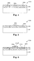
- Figures 4-12 illustrate embodiments for fabricating an array 102 of phase change memory elements 106 with reduced crosstalk as illustrated and described with reference to Figure 3 .
- Figure 4 illustrates a cross-sectional view of one embodiment of substrate 301, contacts 305, and dielectric material 303.
- Substrate 301 may be pre-processed as previously described.
- Dielectric material 303 includes SiO 2 , SiO x , SiN, fluorinated silica glass (FSG), boro-phosphorous silicate glass (BPSG), boro-silicate glass (BSG), or other suitable dielectric material.
- Contacts 305 include TiN, TaN, W, Al, Ti, Ta, TiSiN, TaSiN, TiAIN, TaAlN, Cu, WN, C, or other suitable contact material. Contacts 305 are laterally surrounded by dielectric material 303 on substrate 301.
- Figure 5 illustrates a cross-sectional view of one embodiment of substrate 301, contacts 305a-305b, and dielectric material 303 after changing height of contact 305b with respect to contact 305a.
- the changing of height of contact 305b is performed by a suitable etch process.
- contact 305b and dielectric material 303 is etched by masking contact 305a.
- the etch process is a plasma induced dry etch process.
- the etch process is a wet etch process.
- the change of height is performed by the growth of contact 305a with respect to contact 305b using any suitable deposition technique.
- Figure 6 illustrates a cross-sectional view of one embodiment of substrate 301, contacts 305a-305b, and dielectric materials 303 and 307 after forming electrodes 311a-311b on contacts 305a-305b.
- dielectric material 307 is deposited using chemical vapor deposition (CVD), high density plasma-chemical vapor deposition (HDP-CVD), atomic layer deposition (ALD), metal organic chemical vapor deposition (MOCVD), physical vapor deposition (PVD), jet vapor deposition (JVD), or other suitable deposition technique.
- Dielectric material 307 includes SiO 2 , SiO x , SiN, FSG, BPSG, BSG, or other suitable dielectric material.
- Electrodes 311a-311b are embedded within dielectric material 307 . Electrodes 311a-311b include TiN, TaN, W, Al, Ti, Ta, TiSiN, TaSiN, TiAIN, TaAlN, Cu, WN, C, or other suitable electrode material. Electrodes 311a-311b are embedded by etching portions of the dielectric material 307 to expose contacts 305 and depositing electrode material. In another embodiment, electrodes 311a-311b are formed by depositing electrode material using CVD, HDP-CVD, ALD, MOCVD, PVD, JVD, or other suitable deposition technique. Portions of the electrode material are removed to physically separate electrodes 311a-311b.
- Dielectric material 307 is deposited in between the electrodes 311a-311b using CVD, HDP-CVD, ALD, MOCVD, PVD, JVD, or other suitable deposition technique.
- planarization techniques as chemical mechanical planarization (CMP) are used for removing electrode material or dielectric material.
- phase change material 315 is deposited using CVD, HDP-CVD, ALD, MOCVD, PVD, JVD, or other suitable deposition technique.
- Top electrode 317 is deposited over tise structure using CVD, HDP-CVD, ALD, MOCVD, PVD, JVD, or other suitable deposition technique.
- Top electrode 317 includes TiN, TaN, W, Al, Ti, Ta, TiSiN, TaSiN, TiAIN, TaAlN, Cu, WN, C, or other suitable contact material.
- Figure 7 illustrates a cross-sectional view of another embodiment of an array 102b of phase change memory elements 106 wherein an offset is greater than a thickness of the phase change material 315.
- a first direction is defined by the lateral spacing of interfaces 320a-320b between phase change material 315 and electrodes 311.
- a second direction is defined substantially perpendicular to the first direction. Adjacent interfaces 320a-320b are offset with respect to the second direction. The offset is greater than the thickness of the phase change material 315.
- phase change material at the side of the step 315b between adjacent phase change memory elements has another thickness than on top 315a of electrodes 311.
- phase change material at the side of the step 315b between adjacent memory elements has a thinner thickness than on top 315a of electrodes 311. In one embodiment, this arrangement further reduces crosstalk. In another embodiment, the phase change material 315 vanishes at the sides of the step 315b between adjacent memory elements 106 resulting in physical separation of first interface 320a at the first electrode and second interface 320b at the second electrode.
- Figure 8 illustrates a cross-sectional view of another embodiment of an array 102c of phase change memory elements 106 wherein first interface 320a at the first electrode and the second interface 320b at the second electrode are physically separated.
- a trench 319 is formed by removing phase change material 315 between adjacent phase change memory elements 106.
- removing phase change material 315 between adjacent phase change memory elements 106 is performed by an etch process such as plasma induced dry etch process.
- phase change material 315 is removed by wet etch or other suitable processes.
- trench 319 is filled with dielectric material using CVD, HDP-CVD, ALD, MOCVD, PVD, JVD, or other suitable deposition technique.
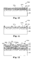
- Figure 9 illustrates a cross-sectional view of another embodiment of substrate 301, electrodes 311a-311b, contacts 305, and dielectric materials 303 and 307.
- Dielectric material 303 and 307 includes SiO 2 , SiO x , SiN, FSG, BPSG, BSG, or other suitable dielectric material.
- Figure 9 corresponds to Figure 6 , besides electrodes 311 a-311b are having no offset.
- Figure 10 illustrates a cross-sectional view of one embodiment of substrate 301, electrodes 311a-311b, contacts 305, and dielectric materials 303 and 307 after depositing a barrier material 313.
- Barrier material 313 is deposited using CVD, HDP-CVD, ALD, MOCVD, PVD, JVD, or other suitable deposition technique.
- a dielectric material such as SiO 2 , porous SiO 2 , aerogel, xerogel, low-k dielectric, SiN, or other suitable dielectric material is used to form barrier material 313.
- Figure 11 illustrates a cross-sectional view of one embodiment of substrate 301, electrodes 311a-311b, contacts 305, dielectric materials 303 and 307, and barrier material 313 after removing a portion of barrier material 313.
- removing of barrier material 313 is performed by an etch process such as plasma induced dry etch process.
- barrier material 313 is removed by wet etch or other suitable processes to remove a portion of barrier material 313. Portions of barrier material 313 are removed to expose electrodes 311a-311b.
- Figure 12 illustrates a cross-sectional view of one embodiment of an array 102d of phase change memory elements 106.
- Phase change material 315 is deposited over the structure illustrated in Figure 11 by using CVD, HDP-CVD, ALD, MOCVD, PVD, JVD, or other suitable deposition technique.
- Direct thermal communication path 330 between interface 320a and interface 320b at electrodes 311 passes through phase change material 315 and around the remaining portions of barrier material 313.
- barrier material 313 has a lower thermal conductivity than resistivity changing material 315.
- barrier material 313 has an equal of higher thermal conductivity than resistivity changing material 315, for which direct thermal communication path 330 still passes around remaining portions of barrier material 313 due to the heat transfer at the boundaries between resistivity changing material 315 and barrier material 313.
- phase change memory elements While the specific embodiments described herein substantially focused on using phase change memory elements, the present invention can be applied to any suitable type of resistivity changing memory elements.
Landscapes
- Semiconductor Memories (AREA)
Abstract
Description
- One type of memory is resistive memory. Resistive memory utilizes the resistance value of a memory element to store one or more bits of data. For example, a memory element programmed to have a high resistance value may represent a logic "1" data bit value and a memory element programmed to have a low resistance value may represent a logic "0" data bit value. Typically, the resistance value of the memory element is switched electrically by applying a voltage pulse or a current pulse to the memory element.
- One type of resistive memory is phase change memory. Phase change memory uses a phase change material in the resistive memory element. The phase change material exhibits at least two different states. The states of the phase change material may be referred to as the amorphous state and the crystalline state, where the amorphous state involves a more disordered atomic structure and the crystalline state involves a more ordered lattice. The amorphous state usually exhibits higher resistivity than the crystalline state. Also, some phase change materials exhibit multiple crystalline states, e.g. a face-centered cubic (FCC) state and a hexagonal closest packing (HCP) state, which have different resistivities and may be used to store bits of data. In the following description, the amorphous state generally refers to the state having the higher resistivity and the crystalline state generally refers to the state having the lower resistivity.
- Phase changes in the phase change materials may be induced reversibly. In this way, the memory may change from the amorphous state to the crystalline state and from the crystalline state to the amorphous state in response to temperature changes. The temperature changes of the phase change material may be achieved by driving current through the phase change material itself or by driving current through a resistive heater adjacent the phase change material. With both of these methods, controllable heating of the phase change material causes controllable phase change within the phase change material.
- A phase change memory including a memory array having a plurality of memory cells that are made of phase change material may be programmed to store data utilizing the memory states of the phase change material. One way to read and write data in such a phase change memory device is to control a current and/or a voltage pulse that is applied to the phase change material. The temperature in the phase change material in each memory cell generally corresponds to the applied level of current and/or voltage to achieve the heating.
- To achieve higher density phase change memories, a phase change memory cell can store multiple bits of data. Multi-bit storage in a phase change memory cell can be achieved by programming the phase change material to have intermediate resistance values or states, where the multi-bit or multilevel phase change memory cell can be written to more than two states. If the phase change memory cell is programmed to one of three different resistance levels, 1.5 bits of data per cell can be stored. If the phase change memory cell is programmed to one of four different resistance levels, two bits of data per cell can be stored, and so on. To program a phase change memory cell to an intermediate resistance value, the amount of crystalline material coexisting with amorphous material and hence the cell resistance is controlled via a suitable write strategy.
- One undesirable feature of resistive memory arrays is electrical and thermal crosstalk between cells. Cross talk between cells might occur with shared storage material geometries such as plate architecture or shared storage material along a bit line. These architectures relax the need for small scale patterning of phase change material and reduce risks due to etch or chemical mechanical planarization (CMP) damage.
- For these and other reasons, there is a need for the present invention.
- One embodiment provides an integrated circuit. The integrated circuit includes a first electrode, a second electrode, a first resistivity changing material contacting the first electrode at a first interface, and a second resistivity changing material contacting the second electrode at a second interface. A direct communication path between the first interface and the second interface is greater than the lateral distance.
- The accompanying drawings are included to provide a further understanding of embodiments and are incorporated in and constitute a part of this specification. The drawings illustrate embodiments and together with the description serve to explain principles of embodiments. Other embodiments and many of the intended advantages of embodiments will be readily appreciated as they become better understood by reference to the following detailed description. The elements of the drawings are not necessarily to scale relative to each other. Like reference numerals designate corresponding similar parts.
-
Figure 1 is a block diagram illustrating one embodiment of a system. -
Figure 2 is a diagram illustrating one embodiment of a memory device. -
Figure 3 illustrates a cross-sectional view of one embodiment of an array of resistivity changing memory elements. -
Figure 4 illustrates a cross-sectional view of one embodiment of a substrate, contacts, and dielectric material. -
Figure 5 illustrates a cross-sectional view of one embodiment of a substrate, contacts, and dielectric material after changing a height of one contact. -
Figure 6 illustrates a cross-sectional view of one embodiment of a substrate, contacts, and dielectric material after forming electrodes on top of the contacts. -
Figure 7 illustrates a cross-sectional view of another embodiment of an array of resistivity changing memory elements wherein an offset is greater than a thickness of resistivity changing material. -
Figure 8 illustrates a cross-sectional view of another embodiment of an array of resistivity changing memory elements wherein storage locations at electrodes are physically separated. -
Figure 9 illustrates a cross-sectional view of another embodiment of a substrate, electrodes, and dielectric material. -
Figure 10 illustrates a cross-sectional view of one embodiment of a substrate, electrodes, and dielectric material after depositing barrier material. -
Figure 11 illustrates a cross-sectional view of one embodiment of a substrate, electrodes, dielectric material, and barrier material after removing a portion of the barrier material. -
Figure 12 illustrates a cross-sectional view of another embodiment of an array of resistivity changing memory elements. - In the following Detailed Description, reference is made to the accompanying drawings, which form a part hereof, and in which is shown by way of illustration specific embodiments in which the invention may be practiced. In this regard, directional terminology, such as "top," "bottom," "front," "back," "leading," "trailing," etc., is used with reference to the orientation of the Figure(s) being described. Because components of embodiments can be positioned in a number of different orientations, the directional terminology is used for purposes of illustration and is in no way limiting. It is to be understood that other embodiments may be utilized and structural or logical changes may be made without departing from the scope of the present invention. The following detailed description, therefore, is not to be taken in a limiting sense, and the scope of the present invention is defined by the appended claims.
- It is to be understood that the features of the various embodiments described herein may be combined with each other, unless specifically noted otherwise.
-
Figure 1 is a block diagram illustrating one embodiment of asystem 90.System 90 includes ahost 92 and amemory device 100.Host 92 is communicatively coupled tomemory device 100 throughcommunication link 94.Host 92 includes a computer (e.g., desktop, laptop, handheld), portable electronic device (e.g., cellular phone, personal digital assistant (PDA), MP3 player, video player, digital camera), or any other suitable device that uses memory.Memory device 100 provides memory forhost 92. In one embodiment,memory device 100 includes a resistivity changing memory device or a phase change memory device. -
Figure 2 is a diagram illustrating one embodiment ofmemory device 100. In one embodiment,memory device 100 is an integrated circuit or part of an integrated circuit.Memory device 100 includes awrite circuit 124, acontroller 120, amemory array 102, and asense circuit 126.Memory array 102 includes a plurality of resistivity changingmemory cells 104a-104d (collectively referred to as resistive memory cells 104), a plurality of bit lines (BLs) 112a-112b (collectively referred to as bit lines 112), a plurality of word lines (WLs) 110a-110b (collectively referred to as word lines 110), and a plurality of ground lines (GLs) 114a-114b (collectively referred to as ground lines 114). In one embodiment, resistivity changing memory cells 104 are phase change memory cells. In other embodiments, resistivity changing memory cells 104 are another suitable type of resistivity changing memory cells, such as magnetic memory cells. - Each phase change memory cell 104 includes a phase
change memory element 106 and a select device 108. Each phasechange memory element 106 includes phase change material and electrodes. Two adjacent phase change memory elements 106 (e.g., 106a and 106b) are spaced apart by a lateral distance. To prevent crosstalk between adjacent and nearby phasechange memory elements 106, a direct communication path between an interface at a first electrode and an interface at a second adjacent electrode is greater than the lateral distance. For phasechange memory elements 106, the crosstalk by a direct communication path is at least one of thermal communication and electrical communication. For another suitable type of resistivity changingmemory elements 106, the direct communication path is one of direct thermal communication, direct electrical communication or any other, suitable direct communication. - As used herein, the term "electrically coupled" is not meant to mean that the elements must be directly coupled together and intervening elements may be provided between the "electrically coupled" elements.
- As used herein, the term "direct communication path" is not meant to mean the nearest spatial connection between two locations and "direct communication path" is that path with the highest transfer rate. For thermal communication, the direct communication path is the path with highest heat transfer. For electrical communication, the direct communication path is the path with highest current transfer.
-
Memory array 102 is electrically coupled to writecircuit 124 throughsignal path 125, tocontroller 120 throughsignal path 121, and tosense circuit 126 throughsignal path 127.Controller 120 is electrically coupled to writecircuit 124 throughsignal path 128 and to sensecircuit 126 throughsignal path 130. Each phase change memory cell 104 is electrically coupled to a word line 110 and a bit line 112. Phasechange memory cell 104a is electrically coupled tobit line 112a andword line 110a, and phasechange memory cell 104b is electrically coupled tobit line 112a andword line 110b. Phasechange memory cell 104c is electrically coupled tobit line 112b andword line 110a, and phasechange memory cell 104d is electrically coupled tobit line 112b andword line 110b. - Each phase change memory cell 104 is electrically coupled to a word line 110, a bit line 112, and a ground line 114. For example, phase
change memory cell 104a is electrically coupled tobit line 112a,word line 110a, andground line 114a, and phasechange memory cell 104b is electrically coupled tobit line 112a,word line 110b, andground line 114b. Phasechange memory cell 104c is electrically coupled tobit line 112b,word line 110a, andground line 114a, and phasechange memory cell 104d is electrically coupled tobit line 112b,word line 110b, andground line 114b. - Each phase change memory cell 104 includes a phase
change memory element 106 and a select device 108. While select device 108 is a field-effect transistor (FET) in the illustrated embodiment, the select device 108 can be other suitable devices such as a bipolar transistor or a 3D transistor structure. In other embodiments, a diode-like structure may be used in place of transistor 108. In this case, a diode andphase change element 106 is coupled in series between each cross point of word lines 110 and bit lines 112. - Phase
change memory cell 104a includes phasechange memory element 106a andtransistor 108a. One side of phasechange memory element 106a is electrically coupled tobit line 112a and the other side of phasechange memory element 106a is electrically coupled to one side of the source-drain path oftransistor 108a. The other side of the source-drain path oftransistor 108a is electrically coupled toground line 114a. The gate oftransistor 108a is electrically coupled toword line 110a. - Phase
change memory cell 104b includes phasechange memory element 106b andtransistor 108b. One side of phasechange memory element 106b is electrically coupled tobit line 112a and the other side of phasechange memory element 106b is electrically coupled to one side of the source-drain path oftransistor 108b. The other side of the source-drain path oftransistor 108b is electrically coupled toground line 114b. The gate oftransistor 108b is electrically coupled toword line 110b. - Phase
change memory cell 104c includes phasechange memory element 106c andtransistor 108c. One side of phasechange memory element 106c is electrically coupled tobit line 112b and the other side of phasechange memory element 106c is electrically coupled to one side of the source-drain path oftransistor 108c. The other side of the source-drain path oftransistor 108c is electrically coupled toground line 114a. The gate oftransistor 108c is electrically coupled toword line 110a. - Phase
change memory cell 104d includes phasechange memory element 106d andtransistor 108d. One side of phasechange memory element 106d is electrically coupled tobit line 112b and the other side of phasechange memory element 106d is electrically coupled to one side of the source-drain path oftransistor 108d. The other side of the source-drain path oftransistor 108d is electrically coupled toground line 114b. The gate oftransistor 108d is electrically coupled toword line 110b. - In one embodiment, each resistivity changing
memory element 106 is a phase change memory element that comprises a phase change material that may be made up of a variety of materials in accordance with the present invention. Generally, chalcogenide alloys that contain one or more elements from Group VI of the periodic table are useful as such materials. In one embodiment, the phase change material is made up of a chalcogenide compound material, such as GeSbTe, SbTe, GeTe, or AgInSbTe. In one embodiment, the phase change material is chalcogen free, such as GeSb, GaSb, InSb, or GeGaInSb. In other embodiments, the phase change material is be made up of any suitable material including one or more of the elements Ge, Sb, Te, Ga, As, In, Se, and S. - Each phase change memory element may be changed from an amorphous state to a crystalline state or from a crystalline state to an amorphous state under the influence of temperature change. The amount of crystalline material coexisting with amorphous material in the phase change material of one of the phase change memory elements thereby defines two or more states for storing data within
memory device 100. In the amorphous state, a phase change material exhibits significantly higher resistivity than in the crystalline state. Therefore, the two or more states of the phase change memory elements differ in their electrical resistivity. In one embodiment, the two or more states are two states and a binary system is used, wherein the two states are assigned bit values of "0" and "1". In another embodiment, the two or more states are three states and a ternary system is used, wherein the three states are assigned bit values of "0", "1", and "2". In another embodiment, the two or more states are four states that are assigned multi-bit values, such as "00", "01", "10", and "11". In other embodiments, the two or more states are another suitable number of states in the phase change material of a phase change memory element. -
Controller 120 includes a microprocessor, microcontroller, or other suitable logic circuitry for controlling the operation ofmemory device 100.Controller 120 controls read and write operations ofmemory device 100 including the application of control and data signals tomemory array 102 throughwrite circuit 124 andsense circuit 126. In one embodiment, writecircuit 124 provides voltage pulses throughsignal path 125 and bit lines 112 to memory cells 104 to program the memory cells. In another embodiment, writecircuit 124 provides current pulses throughsignal path 125 and bit lines 112 to memory cells 104 to program the memory cells. -
Sense circuit 126 reads each of the two or more states of memory cells 104 through bit lines 112 andsignal path 127. In one embodiment, to read the resistance of one of the memory cells 104,sense circuit 126 provides current that flows through one of the memory cells 104.Sense circuit 126 then reads the voltage across that one of the memory cells 104. In another embodiment,sense circuit 126 provides voltage across one of the memory cells 104 and reads the current that flows through that one of the memory cells 104. In another embodiment, writecircuit 124 provides voltage across one of the memory cells 104 andsense circuit 126 reads the current that flows through that one of the memory cells 104. In another embodiment, writecircuit 124 provides current that flows through one of the memory cells 104 andsense circuit 126 reads the voltage across that one of the memory cells 104. - During a "set" operation of phase
change memory cell 104a, a set current or voltage pulse is selectively enabled bywrite circuit 124 and sent throughbit line 112a to phasechange memory element 106a thereby heating phasechange memory element 106a above its crystallization temperature (but usually below its melting temperature). In this way, phasechange memory element 106a reaches its crystalline state or a partially crystalline and partially amorphous state during this set operation. - During a "reset" operation of phase
change memory cell 104a, a reset current or voltage pulse is selectively enabled bywrite circuit 124 and sent throughbit line 112a to phasechange memory element 106a. The reset current or voltage quickly heats phasechange memory element 106a above its melting temperature. After the current or voltage pulse is turned off, phasechange memory element 106a quickly quench cools into the amorphous state or a partially amorphous and partially crystalline state. - Phase
change memory cells 104b-104d and other phase change memory cells 104 inmemory array 102 are set and reset similarly to phasechange memory cell 104a using a similar current or voltage pulse. In other embodiments, for other types of resistive memory cells, writecircuit 124 provides suitable programming pulses to program the resistivity changing memory cells 104 to the desired state. -
Figure 3 illustrates a cross-sectional view of one embodiment of anarray 102a of phasechange memory elements 106. Each phasechange memory element 106 includes anelectrode 311,phase change material 315, and atop electrode 317. In one embodiment, storage locations withinphase change material 315 are located nearby theinterfaces 320a-320b betweenphase change material 315 andelectrodes 311. In another embodiment, the storage locations within thephase change material 315 are located directly atelectrodes 311.Array 102a further includes asubstrate 301 andisolation materials -
Substrate 301 includes Si substrate, Si on insulator (SOI) substrate, or other suitable substrate. In one embodiment,substrate 301 is pre-processed and includes select devices or other devices. In one embodiment,substrate 301 includes select devices 108, such as transistors of any type (e.g., FET or bipolar transistors) or diodes. In another embodiment,substrate 301 includes other suitable devices for semiconductor manufacturing like buried lines, etc. -
Electrode 311 has any suitable shape, such as V-shape, non-regular shape, or cup-shape. In one embodiment,electrode 311 includes more than one material. -
Interfaces 320a-320b betweenphase change material 315 andelectrodes 311 of two adjacent phasechange memory elements 106 are spaced apart by a lateral distance CD. In other embodiments, the lateral distance betweeninterfaces 320a-320b of adjacent phasechange memory elements 106 varies within anarray 102 of phasechange memory elements 106. - In one embodiment,
phase change material 315 extends from oneelectrode 311 toadjacent electrode 311, wherephase change material 315 forms a plate. In other embodiments, phasechange memory elements 106 are physically separated. - In the embodiment illustrated in
Figure 3 , the directthermal communication path 330 betweenfirst interface 320a of a first phasechange memory element 106 andsecond interface 320b of a second phasechange memory element 106 is greater than the lateral distance CD betweenfirst interface 320a andsecond interface 320b by offsetting theinterfaces - Direct
thermal communication path 330 between two adjacent phasechange memory elements 106 is defined as the shortest thermal connection betweenadjacent interfaces 320a-320b betweenphase change material 315 andelectrodes 311. In one embodiment, directthermal communication path 330 is throughresistivity changing material 315 when it extends from electrode to electrode. In another embodiment, directthermal communication path 330 crosses material boundaries. - The following
Figures 4-12 illustrate embodiments for fabricating anarray 102 of phasechange memory elements 106 with reduced crosstalk as illustrated and described with reference toFigure 3 . -
Figure 4 illustrates a cross-sectional view of one embodiment ofsubstrate 301,contacts 305, anddielectric material 303.Substrate 301 may be pre-processed as previously described.Dielectric material 303 includes SiO2, SiOx, SiN, fluorinated silica glass (FSG), boro-phosphorous silicate glass (BPSG), boro-silicate glass (BSG), or other suitable dielectric material.Contacts 305 include TiN, TaN, W, Al, Ti, Ta, TiSiN, TaSiN, TiAIN, TaAlN, Cu, WN, C, or other suitable contact material.Contacts 305 are laterally surrounded bydielectric material 303 onsubstrate 301. -
Figure 5 illustrates a cross-sectional view of one embodiment ofsubstrate 301,contacts 305a-305b, anddielectric material 303 after changing height ofcontact 305b with respect tocontact 305a. The changing of height ofcontact 305b is performed by a suitable etch process. In one embodiment, contact 305b anddielectric material 303 is etched by maskingcontact 305a. In one embodiment, the etch process is a plasma induced dry etch process. In another embodiment, the etch process is a wet etch process. In one embodiment, instead of loweringcontact 305b, the change of height is performed by the growth ofcontact 305a with respect to contact 305b using any suitable deposition technique. -
Figure 6 illustrates a cross-sectional view of one embodiment ofsubstrate 301,contacts 305a-305b, anddielectric materials electrodes 311a-311b oncontacts 305a-305b. In one embodiment,dielectric material 307 is deposited using chemical vapor deposition (CVD), high density plasma-chemical vapor deposition (HDP-CVD), atomic layer deposition (ALD), metal organic chemical vapor deposition (MOCVD), physical vapor deposition (PVD), jet vapor deposition (JVD), or other suitable deposition technique.Dielectric material 307 includes SiO2, SiOx, SiN, FSG, BPSG, BSG, or other suitable dielectric material. Withindielectric material 307electrodes 311a-311b are embedded.Electrodes 311a-311b include TiN, TaN, W, Al, Ti, Ta, TiSiN, TaSiN, TiAIN, TaAlN, Cu, WN, C, or other suitable electrode material.Electrodes 311a-311b are embedded by etching portions of thedielectric material 307 to exposecontacts 305 and depositing electrode material. In another embodiment,electrodes 311a-311b are formed by depositing electrode material using CVD, HDP-CVD, ALD, MOCVD, PVD, JVD, or other suitable deposition technique. Portions of the electrode material are removed to physicallyseparate electrodes 311a-311b.Dielectric material 307 is deposited in between theelectrodes 311a-311b using CVD, HDP-CVD, ALD, MOCVD, PVD, JVD, or other suitable deposition technique. In one embodiment, planarization techniques as chemical mechanical planarization (CMP) are used for removing electrode material or dielectric material. - As illustrated in
Figure 3 , after formingelectrodes 311a-311b oncontacts 305phase change material 315 is deposited using CVD, HDP-CVD, ALD, MOCVD, PVD, JVD, or other suitable deposition technique.Top electrode 317 is deposited over tise structure using CVD, HDP-CVD, ALD, MOCVD, PVD, JVD, or other suitable deposition technique.Top electrode 317 includes TiN, TaN, W, Al, Ti, Ta, TiSiN, TaSiN, TiAIN, TaAlN, Cu, WN, C, or other suitable contact material. -
Figure 7 illustrates a cross-sectional view of another embodiment of anarray 102b of phasechange memory elements 106 wherein an offset is greater than a thickness of thephase change material 315. A first direction is defined by the lateral spacing ofinterfaces 320a-320b betweenphase change material 315 andelectrodes 311. A second direction is defined substantially perpendicular to the first direction.Adjacent interfaces 320a-320b are offset with respect to the second direction. The offset is greater than the thickness of thephase change material 315. In one embodiment, phase change material at the side of thestep 315b between adjacent phase change memory elements has another thickness than on top 315a ofelectrodes 311. In another embodiment, phase change material at the side of thestep 315b between adjacent memory elements has a thinner thickness than on top 315a ofelectrodes 311. In one embodiment, this arrangement further reduces crosstalk. In another embodiment, thephase change material 315 vanishes at the sides of thestep 315b betweenadjacent memory elements 106 resulting in physical separation offirst interface 320a at the first electrode andsecond interface 320b at the second electrode. -
Figure 8 illustrates a cross-sectional view of another embodiment of anarray 102c of phasechange memory elements 106 whereinfirst interface 320a at the first electrode and thesecond interface 320b at the second electrode are physically separated. Atrench 319 is formed by removingphase change material 315 between adjacent phasechange memory elements 106. In one embodiment, removingphase change material 315 between adjacent phasechange memory elements 106 is performed by an etch process such as plasma induced dry etch process. In other embodiments,phase change material 315 is removed by wet etch or other suitable processes. - The direct thermal communication path between
interfaces 320a-320b of adjacent phasechange memory elements 106 crosses the material boundaries betweenresistivity changing material 315 andtrench 319. In one embodiment,trench 319 is filled with dielectric material using CVD, HDP-CVD, ALD, MOCVD, PVD, JVD, or other suitable deposition technique. -
Figure 9 illustrates a cross-sectional view of another embodiment ofsubstrate 301,electrodes 311a-311b,contacts 305, anddielectric materials Dielectric material Figure 9 corresponds toFigure 6 , besideselectrodes 311 a-311b are having no offset. -
Figure 10 illustrates a cross-sectional view of one embodiment ofsubstrate 301,electrodes 311a-311b,contacts 305, anddielectric materials barrier material 313.Barrier material 313 is deposited using CVD, HDP-CVD, ALD, MOCVD, PVD, JVD, or other suitable deposition technique. A dielectric material, such as SiO2, porous SiO2, aerogel, xerogel, low-k dielectric, SiN, or other suitable dielectric material is used to formbarrier material 313. -
Figure 11 illustrates a cross-sectional view of one embodiment ofsubstrate 301,electrodes 311a-311b,contacts 305,dielectric materials barrier material 313 after removing a portion ofbarrier material 313. In one embodiment, removing ofbarrier material 313 is performed by an etch process such as plasma induced dry etch process. In other embodiments,barrier material 313 is removed by wet etch or other suitable processes to remove a portion ofbarrier material 313. Portions ofbarrier material 313 are removed to exposeelectrodes 311a-311b. -
Figure 12 illustrates a cross-sectional view of one embodiment of anarray 102d of phasechange memory elements 106.Phase change material 315 is deposited over the structure illustrated inFigure 11 by using CVD, HDP-CVD, ALD, MOCVD, PVD, JVD, or other suitable deposition technique. Directthermal communication path 330 betweeninterface 320a andinterface 320b atelectrodes 311 passes throughphase change material 315 and around the remaining portions ofbarrier material 313. In one embodiment,barrier material 313 has a lower thermal conductivity thanresistivity changing material 315. In other embodiments,barrier material 313 has an equal of higher thermal conductivity thanresistivity changing material 315, for which directthermal communication path 330 still passes around remaining portions ofbarrier material 313 due to the heat transfer at the boundaries betweenresistivity changing material 315 andbarrier material 313. - While the specific embodiments described herein substantially focused on using phase change memory elements, the present invention can be applied to any suitable type of resistivity changing memory elements.
- Although specific embodiments have been illustrated and described herein, it will be appreciated by those of ordinary skill in the art that a variety of alternate and/or equivalent implementations may be substituted for the specific embodiments shown and described without departing from the scope of the present invention. This application is intended to cover any adaptations or variations of the specific embodiments discussed herein. Therefore, it is intended that this invention be limited only by the claims and the equivalents thereof.
Claims (15)
- An integrated circuit (100) comprising:a first electrode (311a);a second electrode (311b);a first resistivity changing material (315) contacting the first electrode (311a) at a first interface (320a); anda second resistivity changing material (315) contacting the second electrode (311b) at a second interface (320b);wherein the first interface (320a) is spaced apart from the second interface (320b) by a lateral distance (CD), and
wherein a direct communication path (330) between the first interface (320a) and the second interface (320b) is greater than the lateral distance (CD). - The integrated circuit (100) of claim 1, wherein the direct communication path (330) comprises at least one of a thermal communication path and an electrical communication path.
- The integrated circuit (100) of claim 1 to 2, wherein a first direction is defined by the lateral spacing of the first interface (320a) and the second interface (320b),
wherein a second direction is defined substantially perpendicular to the first direction, and
wherein the first interface (320a) and the second interface (320b) are offset with respect to the second direction. - The integrated circuit (100) of claim 3, wherein the offset is greater than a thickness of the resistivity changing material (315).
- The integrated circuit (100) of claim 3 to 4, further comprising:a resistivity changing material (315) extending between the first resistivity changing material (315) and the second resistivity changing material (315).
- The integrated circuit (100) of claim 3 to 5, wherein the resistivity changing material (315) forms a plate of resistivity changing material.
- The integrated circuit (100) of claim 1 to 6, further comprising:a resistivity changing material (315) extending between the first resistivity changing material (315) and the second resistivity changing material (315); anda barrier structure (313) within the resistivity changing material (315).
- The integrated circuit (100) of claim 7, wherein the barrier material (313) has a lower thermal conductivity than the resistivity changing material (315).
- The integrated circuit (100) of claim 7 or 8, wherein the barrier material (313) comprises one of SiO2, porous SiO2, aerogel, xerogel, SiN, and a low-k dielectric.
- The integrated circuit (100) of claim 1 to 9, wherein the resistivity changing material (315) comprises a phase change material.
- A memory comprising:an integrated circuit (100) of claim 1 to 10.
- A system comprising:an integrated circuit (100) of claim 1 to 10.
- A method for fabricating an integrated circuit (100), the method comprising:providing a substrate (301) including a first contact (305a) and a second contact (305b);changing a height of the first contact (305a) with respect to the second contact (305b);forming a first electrode (311a) on the first contact (305a) and a second electrode (311b) on the second contact (305b); anddepositing a resistivity changing material (315) over the first electrode (311a) and the second electrode (311b).
- The method of claim 13, further comprising:removing a portion of the resistivity changing material (315) between the first electrode (311a) and the second electrode (311b) to physically separate a first storage location (320a) at the first electrode (311 a) from a second storage location (320b) at the second electrode (311 b).
- A method for fabricating an integrated circuit (100), the method comprising:providing a substrate (301) including a first electrode (311a), a second electrode (311b), and isolation material (303) between the first electrode (311a) and the second electrode (311b);depositing a barrier material (313) over the first electrode (311 a), the second electrode (311b), and the isolation material (303);removing a portion of the barrier material (313) to expose the first electrode (311a) and the second electrode (311b); anddepositing a resistivity changing material (315) over the first electrode (311a), the second electrode (311b), and the barrier material (313).
Applications Claiming Priority (1)
| Application Number | Priority Date | Filing Date | Title |
|---|---|---|---|
| US11/948,204 US7696510B2 (en) | 2007-11-30 | 2007-11-30 | Integrated circuit including memory having reduced cross talk |
Publications (2)
| Publication Number | Publication Date |
|---|---|
| EP2278621A2 true EP2278621A2 (en) | 2011-01-26 |
| EP2278621A3 EP2278621A3 (en) | 2013-07-31 |
Family
ID=40362817
Family Applications (1)
| Application Number | Title | Priority Date | Filing Date |
|---|---|---|---|
| EP08020434.0A Withdrawn EP2278621A3 (en) | 2007-11-30 | 2008-11-25 | Integrated circuit including memory having reduced cross talk |
Country Status (2)
| Country | Link |
|---|---|
| US (1) | US7696510B2 (en) |
| EP (1) | EP2278621A3 (en) |
Families Citing this family (4)
| Publication number | Priority date | Publication date | Assignee | Title |
|---|---|---|---|---|
| US8203134B2 (en) * | 2009-09-21 | 2012-06-19 | Micron Technology, Inc. | Memory devices with enhanced isolation of memory cells, systems including same and methods of forming same |
| US8629559B2 (en) * | 2012-02-09 | 2014-01-14 | Taiwan Semiconductor Manufacturing Company, Ltd. | Stress reduction apparatus with an inverted cup-shaped layer |
| KR20130131707A (en) * | 2012-05-24 | 2013-12-04 | 에스케이하이닉스 주식회사 | Resistive memory device and fabrication method thereof |
| FR3157058A1 (en) * | 2023-12-13 | 2025-06-20 | Commissariat A L'energie Atomique Et Aux Energies Alternatives | Method of manufacturing a memory device |
Family Cites Families (4)
| Publication number | Priority date | Publication date | Assignee | Title |
|---|---|---|---|---|
| JP2005150243A (en) * | 2003-11-12 | 2005-06-09 | Toshiba Corp | Phase transition memory |
| JP2006156886A (en) * | 2004-12-01 | 2006-06-15 | Renesas Technology Corp | Semiconductor integrated circuit device and manufacturing method thereof |
| WO2007102341A1 (en) * | 2006-03-09 | 2007-09-13 | Matsushita Electric Industrial Co., Ltd. | Resistance-varying type element, semiconductor device, and method for manufacturing the element |
| KR100819560B1 (en) * | 2007-03-26 | 2008-04-08 | 삼성전자주식회사 | Phase change memory device and manufacturing method |
-
2007
- 2007-11-30 US US11/948,204 patent/US7696510B2/en not_active Expired - Fee Related
-
2008
- 2008-11-25 EP EP08020434.0A patent/EP2278621A3/en not_active Withdrawn
Also Published As
| Publication number | Publication date |
|---|---|
| US7696510B2 (en) | 2010-04-13 |
| US20090046498A1 (en) | 2009-02-19 |
| EP2278621A3 (en) | 2013-07-31 |
Similar Documents
| Publication | Publication Date | Title |
|---|---|---|
| US7545668B2 (en) | Mushroom phase change memory having a multilayer electrode | |
| US7786464B2 (en) | Integrated circuit having dielectric layer including nanocrystals | |
| US7875492B2 (en) | Integrated circuit including a memory fabricated using self-aligned processing | |
| US8284596B2 (en) | Integrated circuit including an array of diodes coupled to a layer of resistance changing material | |
| US7362608B2 (en) | Phase change memory fabricated using self-aligned processing | |
| US7838860B2 (en) | Integrated circuit including vertical diode | |
| US8189372B2 (en) | Integrated circuit including electrode having recessed portion | |
| US20080265239A1 (en) | Integrated circuit including spacer material layer | |
| US7495946B2 (en) | Phase change memory fabricated using self-aligned processing | |
| EP1923928A2 (en) | Phase change memory cell having a sidewall contact | |
| US20090185411A1 (en) | Integrated circuit including diode memory cells | |
| US7545019B2 (en) | Integrated circuit including logic portion and memory portion | |
| US8039299B2 (en) | Method for fabricating an integrated circuit including resistivity changing material having a planarized surface | |
| US7671354B2 (en) | Integrated circuit including spacer defined electrode | |
| US8084759B2 (en) | Integrated circuit including doped semiconductor line having conductive cladding | |
| US20080316793A1 (en) | Integrated circuit including contact contacting bottom and sidewall of electrode | |
| CN114566591A (en) | Semiconductor device with a plurality of semiconductor chips | |
| US7760546B2 (en) | Integrated circuit including an electrode having an outer portion with greater resistivity | |
| US7671353B2 (en) | Integrated circuit having contact including material between sidewalls | |
| US7696510B2 (en) | Integrated circuit including memory having reduced cross talk | |
| US7679074B2 (en) | Integrated circuit having multilayer electrode | |
| US20080272354A1 (en) | Phase change diode memory | |
| EP2278635A2 (en) | Method of making memory with resistivity changing material |
Legal Events
| Date | Code | Title | Description |
|---|---|---|---|
| PUAI | Public reference made under article 153(3) epc to a published international application that has entered the european phase |
Free format text: ORIGINAL CODE: 0009012 |
|
| AK | Designated contracting states |
Kind code of ref document: A2 Designated state(s): AT BE BG CH CY CZ DE DK EE ES FI FR GB GR HR HU IE IS IT LI LT LU LV MC MT NL NO PL PT RO SE SI SK TR |
|
| AX | Request for extension of the european patent |
Extension state: AL BA MK RS |
|
| PUAL | Search report despatched |
Free format text: ORIGINAL CODE: 0009013 |
|
| AK | Designated contracting states |
Kind code of ref document: A3 Designated state(s): AT BE BG CH CY CZ DE DK EE ES FI FR GB GR HR HU IE IS IT LI LT LU LV MC MT NL NO PL PT RO SE SI SK TR |
|
| AX | Request for extension of the european patent |
Extension state: AL BA MK RS |
|
| RIC1 | Information provided on ipc code assigned before grant |
Ipc: H01L 27/24 20060101AFI20130624BHEP |
|
| AKY | No designation fees paid | ||
| REG | Reference to a national code |
Ref country code: DE Ref legal event code: R108 |
|
| REG | Reference to a national code |
Ref country code: DE Ref legal event code: R108 Effective date: 20140409 |
|
| STAA | Information on the status of an ep patent application or granted ep patent |
Free format text: STATUS: THE APPLICATION IS DEEMED TO BE WITHDRAWN |
|
| 18D | Application deemed to be withdrawn |
Effective date: 20140201 |