EP2278032A2 - Electrically conductive bonding material, method of bonding with the same, and semiconductor device bonded with the same - Google Patents
Electrically conductive bonding material, method of bonding with the same, and semiconductor device bonded with the same Download PDFInfo
- Publication number
- EP2278032A2 EP2278032A2 EP20100004458 EP10004458A EP2278032A2 EP 2278032 A2 EP2278032 A2 EP 2278032A2 EP 20100004458 EP20100004458 EP 20100004458 EP 10004458 A EP10004458 A EP 10004458A EP 2278032 A2 EP2278032 A2 EP 2278032A2
- Authority
- EP
- European Patent Office
- Prior art keywords
- silver
- particles
- bonding
- electrically conductive
- bonding material
- Prior art date
- Legal status (The legal status is an assumption and is not a legal conclusion. Google has not performed a legal analysis and makes no representation as to the accuracy of the status listed.)
- Withdrawn
Links
Images


Classifications
-
- B—PERFORMING OPERATIONS; TRANSPORTING
- B22—CASTING; POWDER METALLURGY
- B22F—WORKING METALLIC POWDER; MANUFACTURE OF ARTICLES FROM METALLIC POWDER; MAKING METALLIC POWDER; APPARATUS OR DEVICES SPECIALLY ADAPTED FOR METALLIC POWDER
- B22F1/00—Metallic powder; Treatment of metallic powder, e.g. to facilitate working or to improve properties
- B22F1/10—Metallic powder containing lubricating or binding agents; Metallic powder containing organic material
- B22F1/107—Metallic powder containing lubricating or binding agents; Metallic powder containing organic material containing organic material comprising solvents, e.g. for slip casting
-
- H—ELECTRICITY
- H01—ELECTRIC ELEMENTS
- H01B—CABLES; CONDUCTORS; INSULATORS; SELECTION OF MATERIALS FOR THEIR CONDUCTIVE, INSULATING OR DIELECTRIC PROPERTIES
- H01B1/00—Conductors or conductive bodies characterised by the conductive materials; Selection of materials as conductors
- H01B1/20—Conductive material dispersed in non-conductive organic material
- H01B1/22—Conductive material dispersed in non-conductive organic material the conductive material comprising metals or alloys
-
- H—ELECTRICITY
- H10—SEMICONDUCTOR DEVICES; ELECTRIC SOLID-STATE DEVICES NOT OTHERWISE PROVIDED FOR
- H10W—GENERIC PACKAGES, INTERCONNECTIONS, CONNECTORS OR OTHER CONSTRUCTIONAL DETAILS OF DEVICES COVERED BY CLASS H10
- H10W40/00—Arrangements for thermal protection or thermal control
-
- H—ELECTRICITY
- H10—SEMICONDUCTOR DEVICES; ELECTRIC SOLID-STATE DEVICES NOT OTHERWISE PROVIDED FOR
- H10W—GENERIC PACKAGES, INTERCONNECTIONS, CONNECTORS OR OTHER CONSTRUCTIONAL DETAILS OF DEVICES COVERED BY CLASS H10
- H10W40/00—Arrangements for thermal protection or thermal control
- H10W40/20—Arrangements for cooling
- H10W40/25—Arrangements for cooling characterised by their materials
- H10W40/255—Arrangements for cooling characterised by their materials having a laminate or multilayered structure, e.g. direct bond copper [DBC] ceramic substrates
-
- H—ELECTRICITY
- H10—SEMICONDUCTOR DEVICES; ELECTRIC SOLID-STATE DEVICES NOT OTHERWISE PROVIDED FOR
- H10W—GENERIC PACKAGES, INTERCONNECTIONS, CONNECTORS OR OTHER CONSTRUCTIONAL DETAILS OF DEVICES COVERED BY CLASS H10
- H10W70/00—Package substrates; Interposers; Redistribution layers [RDL]
- H10W70/20—Conductive package substrates serving as an interconnection, e.g. metal plates
-
- H—ELECTRICITY
- H10—SEMICONDUCTOR DEVICES; ELECTRIC SOLID-STATE DEVICES NOT OTHERWISE PROVIDED FOR
- H10W—GENERIC PACKAGES, INTERCONNECTIONS, CONNECTORS OR OTHER CONSTRUCTIONAL DETAILS OF DEVICES COVERED BY CLASS H10
- H10W70/00—Package substrates; Interposers; Redistribution layers [RDL]
- H10W70/40—Leadframes
- H10W70/411—Chip-supporting parts, e.g. die pads
- H10W70/417—Bonding materials between chips and die pads
-
- H—ELECTRICITY
- H10—SEMICONDUCTOR DEVICES; ELECTRIC SOLID-STATE DEVICES NOT OTHERWISE PROVIDED FOR
- H10W—GENERIC PACKAGES, INTERCONNECTIONS, CONNECTORS OR OTHER CONSTRUCTIONAL DETAILS OF DEVICES COVERED BY CLASS H10
- H10W70/00—Package substrates; Interposers; Redistribution layers [RDL]
- H10W70/60—Insulating or insulated package substrates; Interposers; Redistribution layers
-
- H—ELECTRICITY
- H10—SEMICONDUCTOR DEVICES; ELECTRIC SOLID-STATE DEVICES NOT OTHERWISE PROVIDED FOR
- H10W—GENERIC PACKAGES, INTERCONNECTIONS, CONNECTORS OR OTHER CONSTRUCTIONAL DETAILS OF DEVICES COVERED BY CLASS H10
- H10W70/00—Package substrates; Interposers; Redistribution layers [RDL]
- H10W70/60—Insulating or insulated package substrates; Interposers; Redistribution layers
- H10W70/67—Insulating or insulated package substrates; Interposers; Redistribution layers characterised by their insulating layers or insulating parts
- H10W70/68—Shapes or dispositions thereof
-
- H—ELECTRICITY
- H10—SEMICONDUCTOR DEVICES; ELECTRIC SOLID-STATE DEVICES NOT OTHERWISE PROVIDED FOR
- H10W—GENERIC PACKAGES, INTERCONNECTIONS, CONNECTORS OR OTHER CONSTRUCTIONAL DETAILS OF DEVICES COVERED BY CLASS H10
- H10W70/00—Package substrates; Interposers; Redistribution layers [RDL]
- H10W70/60—Insulating or insulated package substrates; Interposers; Redistribution layers
- H10W70/67—Insulating or insulated package substrates; Interposers; Redistribution layers characterised by their insulating layers or insulating parts
- H10W70/68—Shapes or dispositions thereof
- H10W70/6875—Shapes or dispositions thereof being on a metallic substrate, e.g. insulated metal substrates [IMS]
-
- H—ELECTRICITY
- H10—SEMICONDUCTOR DEVICES; ELECTRIC SOLID-STATE DEVICES NOT OTHERWISE PROVIDED FOR
- H10W—GENERIC PACKAGES, INTERCONNECTIONS, CONNECTORS OR OTHER CONSTRUCTIONAL DETAILS OF DEVICES COVERED BY CLASS H10
- H10W70/00—Package substrates; Interposers; Redistribution layers [RDL]
- H10W70/60—Insulating or insulated package substrates; Interposers; Redistribution layers
- H10W70/67—Insulating or insulated package substrates; Interposers; Redistribution layers characterised by their insulating layers or insulating parts
- H10W70/69—Insulating materials thereof
- H10W70/692—Ceramics or glasses
-
- H—ELECTRICITY
- H10—SEMICONDUCTOR DEVICES; ELECTRIC SOLID-STATE DEVICES NOT OTHERWISE PROVIDED FOR
- H10W—GENERIC PACKAGES, INTERCONNECTIONS, CONNECTORS OR OTHER CONSTRUCTIONAL DETAILS OF DEVICES COVERED BY CLASS H10
- H10W72/00—Interconnections or connectors in packages
- H10W72/20—Bump connectors, e.g. solder bumps or copper pillars; Dummy bumps; Thermal bumps
-
- H—ELECTRICITY
- H10—SEMICONDUCTOR DEVICES; ELECTRIC SOLID-STATE DEVICES NOT OTHERWISE PROVIDED FOR
- H10W—GENERIC PACKAGES, INTERCONNECTIONS, CONNECTORS OR OTHER CONSTRUCTIONAL DETAILS OF DEVICES COVERED BY CLASS H10
- H10W90/00—Package configurations
-
- H—ELECTRICITY
- H10—SEMICONDUCTOR DEVICES; ELECTRIC SOLID-STATE DEVICES NOT OTHERWISE PROVIDED FOR
- H10W—GENERIC PACKAGES, INTERCONNECTIONS, CONNECTORS OR OTHER CONSTRUCTIONAL DETAILS OF DEVICES COVERED BY CLASS H10
- H10W70/00—Package substrates; Interposers; Redistribution layers [RDL]
- H10W70/40—Leadframes
- H10W70/481—Leadframes for devices being provided for in groups H10D8/00 - H10D48/00
-
- H—ELECTRICITY
- H10—SEMICONDUCTOR DEVICES; ELECTRIC SOLID-STATE DEVICES NOT OTHERWISE PROVIDED FOR
- H10W—GENERIC PACKAGES, INTERCONNECTIONS, CONNECTORS OR OTHER CONSTRUCTIONAL DETAILS OF DEVICES COVERED BY CLASS H10
- H10W70/00—Package substrates; Interposers; Redistribution layers [RDL]
- H10W70/60—Insulating or insulated package substrates; Interposers; Redistribution layers
- H10W70/67—Insulating or insulated package substrates; Interposers; Redistribution layers characterised by their insulating layers or insulating parts
- H10W70/68—Shapes or dispositions thereof
- H10W70/682—Shapes or dispositions thereof comprising holes having chips therein
-
- H—ELECTRICITY
- H10—SEMICONDUCTOR DEVICES; ELECTRIC SOLID-STATE DEVICES NOT OTHERWISE PROVIDED FOR
- H10W—GENERIC PACKAGES, INTERCONNECTIONS, CONNECTORS OR OTHER CONSTRUCTIONAL DETAILS OF DEVICES COVERED BY CLASS H10
- H10W72/00—Interconnections or connectors in packages
- H10W72/01—Manufacture or treatment
- H10W72/013—Manufacture or treatment of die-attach connectors
- H10W72/01321—Manufacture or treatment of die-attach connectors using local deposition
- H10W72/01325—Manufacture or treatment of die-attach connectors using local deposition in solid form
-
- H—ELECTRICITY
- H10—SEMICONDUCTOR DEVICES; ELECTRIC SOLID-STATE DEVICES NOT OTHERWISE PROVIDED FOR
- H10W—GENERIC PACKAGES, INTERCONNECTIONS, CONNECTORS OR OTHER CONSTRUCTIONAL DETAILS OF DEVICES COVERED BY CLASS H10
- H10W72/00—Interconnections or connectors in packages
- H10W72/071—Connecting or disconnecting
- H10W72/073—Connecting or disconnecting of die-attach connectors
- H10W72/07331—Connecting techniques
-
- H—ELECTRICITY
- H10—SEMICONDUCTOR DEVICES; ELECTRIC SOLID-STATE DEVICES NOT OTHERWISE PROVIDED FOR
- H10W—GENERIC PACKAGES, INTERCONNECTIONS, CONNECTORS OR OTHER CONSTRUCTIONAL DETAILS OF DEVICES COVERED BY CLASS H10
- H10W72/00—Interconnections or connectors in packages
- H10W72/071—Connecting or disconnecting
- H10W72/073—Connecting or disconnecting of die-attach connectors
- H10W72/07341—Controlling the bonding environment, e.g. atmosphere composition or temperature
-
- H—ELECTRICITY
- H10—SEMICONDUCTOR DEVICES; ELECTRIC SOLID-STATE DEVICES NOT OTHERWISE PROVIDED FOR
- H10W—GENERIC PACKAGES, INTERCONNECTIONS, CONNECTORS OR OTHER CONSTRUCTIONAL DETAILS OF DEVICES COVERED BY CLASS H10
- H10W72/00—Interconnections or connectors in packages
- H10W72/071—Connecting or disconnecting
- H10W72/073—Connecting or disconnecting of die-attach connectors
- H10W72/07351—Connecting or disconnecting of die-attach connectors characterised by changes in properties of the die-attach connectors during connecting
- H10W72/07355—Connecting or disconnecting of die-attach connectors characterised by changes in properties of the die-attach connectors during connecting changes in materials
-
- H—ELECTRICITY
- H10—SEMICONDUCTOR DEVICES; ELECTRIC SOLID-STATE DEVICES NOT OTHERWISE PROVIDED FOR
- H10W—GENERIC PACKAGES, INTERCONNECTIONS, CONNECTORS OR OTHER CONSTRUCTIONAL DETAILS OF DEVICES COVERED BY CLASS H10
- H10W72/00—Interconnections or connectors in packages
- H10W72/071—Connecting or disconnecting
- H10W72/075—Connecting or disconnecting of bond wires
- H10W72/07531—Techniques
- H10W72/07532—Compression bonding, e.g. thermocompression bonding
- H10W72/07533—Ultrasonic bonding, e.g. thermosonic bonding
-
- H—ELECTRICITY
- H10—SEMICONDUCTOR DEVICES; ELECTRIC SOLID-STATE DEVICES NOT OTHERWISE PROVIDED FOR
- H10W—GENERIC PACKAGES, INTERCONNECTIONS, CONNECTORS OR OTHER CONSTRUCTIONAL DETAILS OF DEVICES COVERED BY CLASS H10
- H10W72/00—Interconnections or connectors in packages
- H10W72/30—Die-attach connectors
- H10W72/321—Structures or relative sizes of die-attach connectors
-
- H—ELECTRICITY
- H10—SEMICONDUCTOR DEVICES; ELECTRIC SOLID-STATE DEVICES NOT OTHERWISE PROVIDED FOR
- H10W—GENERIC PACKAGES, INTERCONNECTIONS, CONNECTORS OR OTHER CONSTRUCTIONAL DETAILS OF DEVICES COVERED BY CLASS H10
- H10W72/00—Interconnections or connectors in packages
- H10W72/30—Die-attach connectors
- H10W72/321—Structures or relative sizes of die-attach connectors
- H10W72/324—Die-attach connectors having multiple side-by-side cores
-
- H—ELECTRICITY
- H10—SEMICONDUCTOR DEVICES; ELECTRIC SOLID-STATE DEVICES NOT OTHERWISE PROVIDED FOR
- H10W—GENERIC PACKAGES, INTERCONNECTIONS, CONNECTORS OR OTHER CONSTRUCTIONAL DETAILS OF DEVICES COVERED BY CLASS H10
- H10W72/00—Interconnections or connectors in packages
- H10W72/30—Die-attach connectors
- H10W72/321—Structures or relative sizes of die-attach connectors
- H10W72/325—Die-attach connectors having a filler embedded in a matrix
-
- H—ELECTRICITY
- H10—SEMICONDUCTOR DEVICES; ELECTRIC SOLID-STATE DEVICES NOT OTHERWISE PROVIDED FOR
- H10W—GENERIC PACKAGES, INTERCONNECTIONS, CONNECTORS OR OTHER CONSTRUCTIONAL DETAILS OF DEVICES COVERED BY CLASS H10
- H10W72/00—Interconnections or connectors in packages
- H10W72/30—Die-attach connectors
- H10W72/331—Shapes of die-attach connectors
-
- H—ELECTRICITY
- H10—SEMICONDUCTOR DEVICES; ELECTRIC SOLID-STATE DEVICES NOT OTHERWISE PROVIDED FOR
- H10W—GENERIC PACKAGES, INTERCONNECTIONS, CONNECTORS OR OTHER CONSTRUCTIONAL DETAILS OF DEVICES COVERED BY CLASS H10
- H10W72/00—Interconnections or connectors in packages
- H10W72/30—Die-attach connectors
- H10W72/351—Materials of die-attach connectors
-
- H—ELECTRICITY
- H10—SEMICONDUCTOR DEVICES; ELECTRIC SOLID-STATE DEVICES NOT OTHERWISE PROVIDED FOR
- H10W—GENERIC PACKAGES, INTERCONNECTIONS, CONNECTORS OR OTHER CONSTRUCTIONAL DETAILS OF DEVICES COVERED BY CLASS H10
- H10W72/00—Interconnections or connectors in packages
- H10W72/30—Die-attach connectors
- H10W72/351—Materials of die-attach connectors
- H10W72/352—Materials of die-attach connectors comprising metals or metalloids, e.g. solders
-
- H—ELECTRICITY
- H10—SEMICONDUCTOR DEVICES; ELECTRIC SOLID-STATE DEVICES NOT OTHERWISE PROVIDED FOR
- H10W—GENERIC PACKAGES, INTERCONNECTIONS, CONNECTORS OR OTHER CONSTRUCTIONAL DETAILS OF DEVICES COVERED BY CLASS H10
- H10W72/00—Interconnections or connectors in packages
- H10W72/30—Die-attach connectors
- H10W72/351—Materials of die-attach connectors
- H10W72/353—Materials of die-attach connectors not comprising solid metals or solid metalloids, e.g. ceramics
-
- H—ELECTRICITY
- H10—SEMICONDUCTOR DEVICES; ELECTRIC SOLID-STATE DEVICES NOT OTHERWISE PROVIDED FOR
- H10W—GENERIC PACKAGES, INTERCONNECTIONS, CONNECTORS OR OTHER CONSTRUCTIONAL DETAILS OF DEVICES COVERED BY CLASS H10
- H10W72/00—Interconnections or connectors in packages
- H10W72/30—Die-attach connectors
- H10W72/351—Materials of die-attach connectors
- H10W72/353—Materials of die-attach connectors not comprising solid metals or solid metalloids, e.g. ceramics
- H10W72/354—Materials of die-attach connectors not comprising solid metals or solid metalloids, e.g. ceramics comprising polymers
-
- H—ELECTRICITY
- H10—SEMICONDUCTOR DEVICES; ELECTRIC SOLID-STATE DEVICES NOT OTHERWISE PROVIDED FOR
- H10W—GENERIC PACKAGES, INTERCONNECTIONS, CONNECTORS OR OTHER CONSTRUCTIONAL DETAILS OF DEVICES COVERED BY CLASS H10
- H10W72/00—Interconnections or connectors in packages
- H10W72/30—Die-attach connectors
- H10W72/351—Materials of die-attach connectors
- H10W72/355—Materials of die-attach connectors of outermost layers of multilayered die-attach connectors, e.g. material of a coating
-
- H—ELECTRICITY
- H10—SEMICONDUCTOR DEVICES; ELECTRIC SOLID-STATE DEVICES NOT OTHERWISE PROVIDED FOR
- H10W—GENERIC PACKAGES, INTERCONNECTIONS, CONNECTORS OR OTHER CONSTRUCTIONAL DETAILS OF DEVICES COVERED BY CLASS H10
- H10W72/00—Interconnections or connectors in packages
- H10W72/50—Bond wires
- H10W72/531—Shapes of wire connectors
- H10W72/5363—Shapes of wire connectors the connected ends being wedge-shaped
-
- H—ELECTRICITY
- H10—SEMICONDUCTOR DEVICES; ELECTRIC SOLID-STATE DEVICES NOT OTHERWISE PROVIDED FOR
- H10W—GENERIC PACKAGES, INTERCONNECTIONS, CONNECTORS OR OTHER CONSTRUCTIONAL DETAILS OF DEVICES COVERED BY CLASS H10
- H10W72/00—Interconnections or connectors in packages
- H10W72/50—Bond wires
- H10W72/541—Dispositions of bond wires
- H10W72/5445—Dispositions of bond wires being orthogonal to a side surface of the chip, e.g. parallel arrangements
-
- H—ELECTRICITY
- H10—SEMICONDUCTOR DEVICES; ELECTRIC SOLID-STATE DEVICES NOT OTHERWISE PROVIDED FOR
- H10W—GENERIC PACKAGES, INTERCONNECTIONS, CONNECTORS OR OTHER CONSTRUCTIONAL DETAILS OF DEVICES COVERED BY CLASS H10
- H10W72/00—Interconnections or connectors in packages
- H10W72/50—Bond wires
- H10W72/541—Dispositions of bond wires
- H10W72/547—Dispositions of multiple bond wires
- H10W72/5475—Dispositions of multiple bond wires multiple bond wires connected to common bond pads at both ends of the wires
-
- H—ELECTRICITY
- H10—SEMICONDUCTOR DEVICES; ELECTRIC SOLID-STATE DEVICES NOT OTHERWISE PROVIDED FOR
- H10W—GENERIC PACKAGES, INTERCONNECTIONS, CONNECTORS OR OTHER CONSTRUCTIONAL DETAILS OF DEVICES COVERED BY CLASS H10
- H10W72/00—Interconnections or connectors in packages
- H10W72/50—Bond wires
- H10W72/551—Materials of bond wires
- H10W72/552—Materials of bond wires comprising metals or metalloids, e.g. silver
- H10W72/5524—Materials of bond wires comprising metals or metalloids, e.g. silver comprising aluminium [Al]
-
- H—ELECTRICITY
- H10—SEMICONDUCTOR DEVICES; ELECTRIC SOLID-STATE DEVICES NOT OTHERWISE PROVIDED FOR
- H10W—GENERIC PACKAGES, INTERCONNECTIONS, CONNECTORS OR OTHER CONSTRUCTIONAL DETAILS OF DEVICES COVERED BY CLASS H10
- H10W72/00—Interconnections or connectors in packages
- H10W72/50—Bond wires
- H10W72/551—Materials of bond wires
- H10W72/552—Materials of bond wires comprising metals or metalloids, e.g. silver
- H10W72/5525—Materials of bond wires comprising metals or metalloids, e.g. silver comprising copper [Cu]
-
- H—ELECTRICITY
- H10—SEMICONDUCTOR DEVICES; ELECTRIC SOLID-STATE DEVICES NOT OTHERWISE PROVIDED FOR
- H10W—GENERIC PACKAGES, INTERCONNECTIONS, CONNECTORS OR OTHER CONSTRUCTIONAL DETAILS OF DEVICES COVERED BY CLASS H10
- H10W72/00—Interconnections or connectors in packages
- H10W72/50—Bond wires
- H10W72/59—Bond pads specially adapted therefor
-
- H—ELECTRICITY
- H10—SEMICONDUCTOR DEVICES; ELECTRIC SOLID-STATE DEVICES NOT OTHERWISE PROVIDED FOR
- H10W—GENERIC PACKAGES, INTERCONNECTIONS, CONNECTORS OR OTHER CONSTRUCTIONAL DETAILS OF DEVICES COVERED BY CLASS H10
- H10W72/00—Interconnections or connectors in packages
- H10W72/851—Dispositions of multiple connectors or interconnections
- H10W72/874—On different surfaces
- H10W72/884—Die-attach connectors and bond wires
-
- H—ELECTRICITY
- H10—SEMICONDUCTOR DEVICES; ELECTRIC SOLID-STATE DEVICES NOT OTHERWISE PROVIDED FOR
- H10W—GENERIC PACKAGES, INTERCONNECTIONS, CONNECTORS OR OTHER CONSTRUCTIONAL DETAILS OF DEVICES COVERED BY CLASS H10
- H10W72/00—Interconnections or connectors in packages
- H10W72/90—Bond pads, in general
- H10W72/921—Structures or relative sizes of bond pads
- H10W72/923—Bond pads having multiple stacked layers
-
- H—ELECTRICITY
- H10—SEMICONDUCTOR DEVICES; ELECTRIC SOLID-STATE DEVICES NOT OTHERWISE PROVIDED FOR
- H10W—GENERIC PACKAGES, INTERCONNECTIONS, CONNECTORS OR OTHER CONSTRUCTIONAL DETAILS OF DEVICES COVERED BY CLASS H10
- H10W72/00—Interconnections or connectors in packages
- H10W72/90—Bond pads, in general
- H10W72/951—Materials of bond pads
- H10W72/952—Materials of bond pads comprising metals or metalloids, e.g. PbSn, Ag or Cu
-
- H—ELECTRICITY
- H10—SEMICONDUCTOR DEVICES; ELECTRIC SOLID-STATE DEVICES NOT OTHERWISE PROVIDED FOR
- H10W—GENERIC PACKAGES, INTERCONNECTIONS, CONNECTORS OR OTHER CONSTRUCTIONAL DETAILS OF DEVICES COVERED BY CLASS H10
- H10W74/00—Encapsulations, e.g. protective coatings
-
- H—ELECTRICITY
- H10—SEMICONDUCTOR DEVICES; ELECTRIC SOLID-STATE DEVICES NOT OTHERWISE PROVIDED FOR
- H10W—GENERIC PACKAGES, INTERCONNECTIONS, CONNECTORS OR OTHER CONSTRUCTIONAL DETAILS OF DEVICES COVERED BY CLASS H10
- H10W74/00—Encapsulations, e.g. protective coatings
- H10W74/01—Manufacture or treatment
- H10W74/016—Manufacture or treatment using moulds
-
- H—ELECTRICITY
- H10—SEMICONDUCTOR DEVICES; ELECTRIC SOLID-STATE DEVICES NOT OTHERWISE PROVIDED FOR
- H10W—GENERIC PACKAGES, INTERCONNECTIONS, CONNECTORS OR OTHER CONSTRUCTIONAL DETAILS OF DEVICES COVERED BY CLASS H10
- H10W74/00—Encapsulations, e.g. protective coatings
- H10W74/10—Encapsulations, e.g. protective coatings characterised by their shape or disposition
- H10W74/111—Encapsulations, e.g. protective coatings characterised by their shape or disposition the semiconductor body being completely enclosed
-
- H—ELECTRICITY
- H10—SEMICONDUCTOR DEVICES; ELECTRIC SOLID-STATE DEVICES NOT OTHERWISE PROVIDED FOR
- H10W—GENERIC PACKAGES, INTERCONNECTIONS, CONNECTORS OR OTHER CONSTRUCTIONAL DETAILS OF DEVICES COVERED BY CLASS H10
- H10W74/00—Encapsulations, e.g. protective coatings
- H10W74/10—Encapsulations, e.g. protective coatings characterised by their shape or disposition
- H10W74/111—Encapsulations, e.g. protective coatings characterised by their shape or disposition the semiconductor body being completely enclosed
- H10W74/114—Encapsulations, e.g. protective coatings characterised by their shape or disposition the semiconductor body being completely enclosed by a substrate and the encapsulations
-
- H—ELECTRICITY
- H10—SEMICONDUCTOR DEVICES; ELECTRIC SOLID-STATE DEVICES NOT OTHERWISE PROVIDED FOR
- H10W—GENERIC PACKAGES, INTERCONNECTIONS, CONNECTORS OR OTHER CONSTRUCTIONAL DETAILS OF DEVICES COVERED BY CLASS H10
- H10W76/00—Containers; Fillings or auxiliary members therefor; Seals
- H10W76/10—Containers or parts thereof
- H10W76/12—Containers or parts thereof characterised by their shape
- H10W76/13—Containers comprising a conductive base serving as an interconnection
- H10W76/136—Containers comprising a conductive base serving as an interconnection having other interconnections perpendicular to the conductive base
-
- H—ELECTRICITY
- H10—SEMICONDUCTOR DEVICES; ELECTRIC SOLID-STATE DEVICES NOT OTHERWISE PROVIDED FOR
- H10W—GENERIC PACKAGES, INTERCONNECTIONS, CONNECTORS OR OTHER CONSTRUCTIONAL DETAILS OF DEVICES COVERED BY CLASS H10
- H10W76/00—Containers; Fillings or auxiliary members therefor; Seals
- H10W76/40—Fillings or auxiliary members in containers, e.g. centering rings
- H10W76/42—Fillings
- H10W76/47—Solid or gel fillings
-
- H—ELECTRICITY
- H10—SEMICONDUCTOR DEVICES; ELECTRIC SOLID-STATE DEVICES NOT OTHERWISE PROVIDED FOR
- H10W—GENERIC PACKAGES, INTERCONNECTIONS, CONNECTORS OR OTHER CONSTRUCTIONAL DETAILS OF DEVICES COVERED BY CLASS H10
- H10W76/00—Containers; Fillings or auxiliary members therefor; Seals
- H10W76/60—Seals
-
- H—ELECTRICITY
- H10—SEMICONDUCTOR DEVICES; ELECTRIC SOLID-STATE DEVICES NOT OTHERWISE PROVIDED FOR
- H10W—GENERIC PACKAGES, INTERCONNECTIONS, CONNECTORS OR OTHER CONSTRUCTIONAL DETAILS OF DEVICES COVERED BY CLASS H10
- H10W90/00—Package configurations
- H10W90/701—Package configurations characterised by the relative positions of pads or connectors relative to package parts
- H10W90/731—Package configurations characterised by the relative positions of pads or connectors relative to package parts of die-attach connectors
- H10W90/734—Package configurations characterised by the relative positions of pads or connectors relative to package parts of die-attach connectors between a chip and a stacked insulating package substrate, interposer or RDL
-
- H—ELECTRICITY
- H10—SEMICONDUCTOR DEVICES; ELECTRIC SOLID-STATE DEVICES NOT OTHERWISE PROVIDED FOR
- H10W—GENERIC PACKAGES, INTERCONNECTIONS, CONNECTORS OR OTHER CONSTRUCTIONAL DETAILS OF DEVICES COVERED BY CLASS H10
- H10W90/00—Package configurations
- H10W90/701—Package configurations characterised by the relative positions of pads or connectors relative to package parts
- H10W90/731—Package configurations characterised by the relative positions of pads or connectors relative to package parts of die-attach connectors
- H10W90/736—Package configurations characterised by the relative positions of pads or connectors relative to package parts of die-attach connectors between a chip and a stacked lead frame, conducting package substrate or heat sink
-
- H—ELECTRICITY
- H10—SEMICONDUCTOR DEVICES; ELECTRIC SOLID-STATE DEVICES NOT OTHERWISE PROVIDED FOR
- H10W—GENERIC PACKAGES, INTERCONNECTIONS, CONNECTORS OR OTHER CONSTRUCTIONAL DETAILS OF DEVICES COVERED BY CLASS H10
- H10W90/00—Package configurations
- H10W90/701—Package configurations characterised by the relative positions of pads or connectors relative to package parts
- H10W90/751—Package configurations characterised by the relative positions of pads or connectors relative to package parts of bond wires
- H10W90/754—Package configurations characterised by the relative positions of pads or connectors relative to package parts of bond wires between a chip and a stacked insulating package substrate, interposer or RDL
-
- H—ELECTRICITY
- H10—SEMICONDUCTOR DEVICES; ELECTRIC SOLID-STATE DEVICES NOT OTHERWISE PROVIDED FOR
- H10W—GENERIC PACKAGES, INTERCONNECTIONS, CONNECTORS OR OTHER CONSTRUCTIONAL DETAILS OF DEVICES COVERED BY CLASS H10
- H10W90/00—Package configurations
- H10W90/701—Package configurations characterised by the relative positions of pads or connectors relative to package parts
- H10W90/751—Package configurations characterised by the relative positions of pads or connectors relative to package parts of bond wires
- H10W90/756—Package configurations characterised by the relative positions of pads or connectors relative to package parts of bond wires between a chip and a stacked lead frame, conducting package substrate or heat sink
Definitions
- the present invention relates to an electrically conductive bonding material, a method of bonding with the same, and a semiconductor device bonded with the same.
- the invention relates to a bonding material and a method of bonding used in a semiconductor module.
- an anchoring member for attaching a semiconductor element functions as an electrode of the semiconductor device.
- the anchoring member base member
- the collector electrode carries an electric current of several or more amperes, resulting in heating the transistor chip.
- a good heat dissipation capacity and a long-term reliability (heat resistance) have to be secured in the soldered portion.
- a material with high heat dissipation is required for securing the heat resistance and heat dissipation performance in a soldered portion.
- a bonding temperature may cause an anchoring member to get damaged by heat or may cause a warp of an entire semiconductor device due to a difference in stress between a substrate and the anchoring member during a cooling period after bonding. That means heat resistance of a bonding material needs to be enhanced while bonding temperature needs to be lowered.
- an electrically conductive bonding material which is an electrically conductive composition containing a granular silver compound is known as a bonding material having a high heat dissipation capacity and a high reliability.
- JP Patent Publication (Kokai) No. 2005-129303 a method for sintering particles having sizes in a range of 1 ⁇ m to 100 ⁇ m in a bonding layer is disclosed.
- a metal particle having a particle size of not greater than 100 nm with few constituent atoms has a sharply increased ratio of surface area to volume of the particle, so that the sintering temperature is substantially reduced compared to that of a bulk form (resulting in increased sintering performance or increased surface energy).
- JP Patent Publication No. 2004-107728 discloses that metal particles having an average particle size of not greater than 100 nm coated with an organic material are used as bonding material and bonding is performed by sintering the metal particles with each other through decomposition of the organic material by heat, utilizing this low-temperature sintering effect. According to this method of bonding, the metal particles after bonding are transformed into bulk metal and moreover the bonding interface is connected by metal bonding, so that the interface has very high heat resistance and reliability, and a high heat dissipation capacity.
- the bonding material disclosed in JP Patent Publication No. 2004-107728 is composed of metal particles having an average particle size of not greater than 100 nm, the bonding interface connected by metal bonding has high heat resistance, reliability, and high heat dissipation capacity, as described above.
- the highly fine metal particles having an average particle size of not greater than 100 nm tend to aggregate.
- Such metal particles need formation of a protective film composed of an organic material for stabilization.
- This protective film composed of an organic material needs to be removed when bonding is performed. Since a large amount of organic material volatilizes from the particle surface to cause volume contraction on this occasion, application of pressure is required during bonding. The applied pressure during bonding may cause damage to a semiconductor chip.
- the method of bonding with metal particles having an average particle size of not greater than 100 nm has practical problems in preparing metal particles, removing impurities after preparation, storing, and handling.
- the present invention has been made taking such circumstance into consideration and provides an electrically conductive bonding material that has high heat resistance after bonding, enables a metal bonding at a bonding interface at a lower temperature as compared to an electrically conductive bonding materials containing a resin, and enables bonding in the absence of pressure not requiring application of pressure during a bonding process; a bonding method with the same; and a semiconductor device bonded with the same.
- a metal bonding in a bonding portion is produced with silver powder (particles) and silver oxide powder (particles) having a particle size of 0.1 ⁇ m to 100 ⁇ m (micro particles), which have not been taken into consideration heretofore.
- simplification of a bonding process is achieved by avoiding use of a resin (reducing a content of organic material), thereby allowing elimination of pressure application during the bonding process.
- solder Although use of lead-free solder is preferred, no alternative material is available for high-temperature soldering. Since hierarchical soldering is indispensable in packaging technology, an alternative material for high-temperature soldering is desired. Accordingly, the bonding technology of the present invention is expected to provide the alternative material for high-temperature soldering.
- an electrically conductive bonding material comprising (A) silver powder, (B) silver oxide powder, and (C) a dispersant composed of an organic material containing not more than 30 carbon atoms as essential components, wherein a total amount of the (A) silver powder, the (B) silver oxide powder, and the (C) dispersant composed of an organic material containing not more than 30 carbon atoms is in a range of 99.0% to 100% by weight of the whole electrically conductive bonding material, enables silver particles to start sintering at a low temperature not higher than 200°C and enables bonding without application of pressure.
- the blended silver oxide particles are reduced to silver by a redox reaction with the dispersant composed of organic material at a temperature not higher than 150°C so as to cause fusion, which promotes sintering at a temperature not higher than 200°C.
- bonding strength is further improved compared to the case in which silver particles are used alone.
- the present inventors found that the silver particles and the silver reduced from the silver oxide used as the bonding material enable bonding to an electrode to be connected without using a resin binder.
- the electrically conductive bonding material of the present invention comprises silver particles, silver oxides particles, and a dispersant composed of an organic material containing not more than 30 carbon atoms as essential components, wherein a total amount of the silver particles, the silver oxide particles, and the dispersant is in a range of 99.0% to 100% by weight.
- the silver particles and the silver oxide particles have particle sizes of 0.1 ⁇ m to 100 ⁇ m (both inclusive).
- the silver particles may be in flake form.
- At least one of the silver particles and the silver oxide particles are coated with a dispersant.
- an amount of the silver oxide particles is not more than an amount of the dispersant.
- the silver particles and the silver oxide particles are in the ratio of 100 mass parts of the silver particles to 0.01 mass parts to 100 mass parts (both inclusive) of the silver oxide particles.
- the electrically conductive bonding material comprises silver particles, silver oxides particles, a dispersant composed of an organic material containing not more than 30 carbon atoms, and an organic solvent having a boiling point of not higher than 350°C as essential components, wherein when a total amount of the silver particles, the silver oxide particles, the dispersant, and the organic solvent is 100 mass parts, an amount of the organic solvent is not more than 90 mass parts, and a total amount of the silver particles, the silver oxide particles, the dispersant, and the organic solvent is in a range of 99.0% to 100% by weight in paste form.
- the electrically conductive bonding material comprises silver particles, silver oxides particles, a dispersant composed of organic material containing not more than 30 carbon atoms, and metal particles of other than silver as essential components, wherein the total amount of the silver particles, the silver oxide particles, the dispersant, and the metal particles of other than silver is 99.0% to 100% by weight.
- the electrically conductive bonding material comprises silver particles, silver oxides particles, a dispersant composed of an organic material containing not more than 30 carbon atoms, an organic solvent having a boiling point of not higher than 350°C, and metal particles of other than silver as essential components, wherein when a total amount of the silver particles, the silver oxide particles, the dispersant, the organic solvent, the organic solvent, and the metal particles is 100 mass parts, an amount of the organic solvent is not more than 90 mass parts, and a total amount of the silver particles, the silver oxide particles, the dispersant, the organic solvent, and the metal particles of other than silver is in a range of 99.0% to 100% by weight.
- the bonding material is in paste form.
- the semiconductor device of the present invention is bonded by any one of the electrically conductive bonding materials described above, and the bonding portion is composed of a metal part alone with a porosity of higher than 0.1% and lower than 90%.
- any one of the electrically conductive bonding material described above is disposed between an electrode of a semiconductor element and a metal member and sintered by heating in an atmosphere of hydrogen, nitrogen, or argon, so that the electrode of the semiconductor element and the metal member are metal bonded.
- the present invention can provide a bonding material and a method of bonding for enabling a metal bonding at a bonding interface at a lower temperature compared to a bonding material with metal particles having an average particle size of not greater than 100 nm. Since a resin binder is not used, a bonding process without application of pressure can be provided for producing a bonding portion having high heat resistance and high heat dissipation after bonding.
- composition of the bonding material relates to an electrically conductive bonding material comprising (A) silver powder, (B) silver oxide powder, and (C) a dispersant composed of an organic material containing not more than 30 carbon atoms as essential components.
- an electrically conductive bonding material with such a composition a total amount of (A) silver powder, (B) silver oxide powder, and (C) the dispersant composed of an organic material containing not more than 30 carbon atoms is in a range of 99.0% to 100% by weight. In other words, a conventional resin is not contained in the composition.
- the electrically conductive bonding material is heated to sinter the silver particles and the silver oxide particles, so that a metal bonding is formed.
- Blending silver powder with silver oxide gives a dispersant and silver oxide a redox reaction during bonding at a temperature not higher than 150°C. Since the reaction promotes sintering of the silver powder, bonding strength at low temperature can be improved.
- the bonding portion can have high heat resistance and high heat dissipation capacity after bonding. Since such a metal bonding can be produced at a low temperature, the bonding material of the present invention can be applied to, for example, bonding an electrode disposed on an active area of a semiconductor element and a mounting part of an interconnecting substrate for mounting the device.
- the bonding layer after bonding has higher a heat resistance compared to the conventional solder material, no melting problem in a portion mounting a semiconductor element occurs in a thermal process such as secondary packaging. A downsized and highly-reliable semiconductor device can be thereby produced.
- the bonding material can substantially improve bonding strength without application of pressure compared to a material of metal nanoparticles having an average particle size of not greater than 100 nm.
- the metal bonding without application of pressure which was difficult to achieve by conventional technology, can substantially simplify the bonding process due to omission of the process for application of pressure during bonding. Since no pressure is applied during bonding, damage to a semiconductor chip during bonding can be substantially reduced.
- the silver particles and the silver oxide particles for use have an average particle size of not smaller than 0.1 ⁇ m and not greater than 100 ⁇ m.
- Metal particles having an average particle size of greater than 100 ⁇ m have low dispersibility in the electrically conductive bonding material, so that a dense bonding layer cannot be produced.
- the average particle size is set at not smaller than 0.1 ⁇ m, because metal particles having an average particle size of smaller than 0.1 ⁇ m need to have their circumference coated with a large amount of organic material in order to prevent the particles from attaching each other in a normal condition and in the cases that such particles are used for bonding, volume contraction occurs while removing the organic material, so that bonding without application of pressure becomes difficult.
- silver oxide particles examples include Ag 2 O and AgO.
- a bonding material composed of at least one or two metals may be used.
- Metal oxides composed of gold oxide and copper oxide may be added concurrently with silver oxide particles for use.
- the particles of silver oxide and silver for use may be in form of flake.
- silver particles alone is in form of flake.
- An average particle size of the flake is preferably not greater than 100 ⁇ m, more preferably not greater than 50 ⁇ m, and most preferably not greater than 10 ⁇ m.
- the preferred lower limit is greater than or equal to 0.1 ⁇ m. Flakes having an average particle size of greater than 100 ⁇ m may cause clogging in mesh for screen printing or reduce stability of storage paste by sedimentation of the particles in form of flake. Meanwhile, particles in form of flake having an average particle size of smaller than 0.1 ⁇ m may not be filled enough due to high viscosity of the paste.
- the particles in form of flake have an average thickness of, preferably not greater than 5.0 ⁇ m and more preferably not greater than 1 ⁇ m.
- the lower limit is not specifically limited and preferably greater than or equal to 0.1 ⁇ m. Flakes having an average thickness of greater than 2.0 ⁇ m may have reduced electrical conductivity due to a reduced aspect ratio.
- An aspect ratio of the particles in form of flake is preferably greater than 1.0 and more preferably 2 or greater.
- An upper limit is not specifically determined, preferably not greater than 200, and more preferably not greater than 150.
- Shapes of the particles are not limited to a sphere or a flake as described above.
- a tetrahedron, an octahedron, a rod, and a fiber may be used. Particles in form of flake can make a surface contact each other so as to increase the contact area.
- a blending ratio of silver oxide particles to silver particles is in a range of 0.01 mass parts to 100 mass parts (both inclusive) of silver oxide particles relative to 100 mass parts (% by weight) of silver particles.
- the blending ratio is set at not smaller than 0.01 mass parts, because the quantities of silver reduced from silver oxide is not enough for the effect of fusing silver at a low temperature with an amount of silver oxide of less than 0.01 mass parts.
- the blending ratio is set at not greater than 100 mass parts, because the increased portion of volume contraction in a bonding layer causes bonding strength to be reduced with an amount of silver oxide of more than 100 mass parts.
- a preferred ratio of silver oxide is about 40% by weight (see FIG. 3 ).
- Examples of a dispersant (and also reducing agent for silver oxide) composed of an organic material containing not more than 30 carbon atoms include mixtures of at least one constituent selected from alcohols, carboxylic acids, and amines. The mixtures coat the circumference of the blended metal particles with an organic material to improve dispersibility of the particles in an organic solvent.
- a dispersant and also reducing agent for silver oxide
- the mixtures coat the circumference of the blended metal particles with an organic material to improve dispersibility of the particles in an organic solvent.
- stearic acid is used as a dispersant for preventing silver particles from attaching to each other, stearic acid is removed from the silver particles by reducing reaction of silver oxide and stearic acid attaching to silver particles at a temperature of 140°C to 150°C.
- a blending ratio of silver oxide to the dispersant is preferably at most 1:1.
- the number of carbon atoms is limited to not more than 30, since an excessive number of carbon atoms cause the boiling point of dispersant to rise and the remaining dispersant in the bonding portion after heating (e.g. 200°C) during bonding may cause problems in bonding strength and reliability.
- Examples of available compounds comprising an alcohol group include alkyl alcohol such as ethanol, propanol, butyl alcohol, pentyl alcohol, hexyl alcohol, heptyl alcohol, octyl alcohol, nonyl alcohol, decyl alcohol, undecyl alcohol, dodecyl alcoho 1, tridecyl alcohol, tetradecyl alcohol, pentadecyl alcohol, hexadecyl alcohol, heptadecyl alcohol, octadecyl alcohol, nonadecyl alcohol, and icosyl alcohol.
- alkyl alcohol such as ethanol, propanol, butyl alcohol, pentyl alcohol, hexyl alcohol, heptyl alcohol, octyl alcohol, nonyl alcohol, decyl alcohol, undecyl alcohol, dodecyl alcoho 1, tridecyl alcohol, tetradecyl alcohol, pentadecyl
- primary alcohols secondary alcohols, tertiary alcohols, alkane diol, or cyclic alcohol compounds may be used.
- ethylene glycol, triethylene glycol or compounds having many alcohol groups such as citric acid, ascorbic acid, and glucose may be used.
- Examples of available compounds containing carboxylic acid include alkylcarboxylic acids such as butanoic acid, pentanoic acid, hexanoic acid, heptanoic acid, octanoic acid, nonanoic acid, decanoic acid, undecanoic acid, dodecanoic acid, tridecanoic acid, tetradecanoic acid, pentadecanoic acid, hexadecanoic acid, heptadecanoic acid, octadecanoic acid, nonadecane acid, icosanoic acid, and oleic acid.
- alkylcarboxylic acids such as butanoic acid, pentanoic acid, hexanoic acid, heptanoic acid, octanoic acid, nonanoic acid, decanoic acid, undecanoic acid, dodecanoic acid, tridecanoic acid, tetradecanoic acid, pen
- examples of available compounds containing an amino group include alkylamines such as butylamine, pentylamine, hexylamine, heptylamine, octylamine, nonylamine, decylamine, undecylamine, dodecylamine, tridecylamin, tetradecylamine, pentadecylamine, hexadecylamine, heptadecylamine, octadecylamine, nonadecylamine, and icodecylamine.
- the compounds having an amino group may have a branching structure.
- Example of such compounds include 2-ethyl hexylamine and 1, 5-dimethylhexylamine.
- secondary amines or tertiary amines may be used.
- such an organic material may have a cyclic structure.
- the dispersants for use are not limited to organic materials including alcohols, carboxylic acids, and amines.
- Organic materials containing an aldehyde group, an ester group, a sulfanyl group, or a ketone group may be used.
- Coating here means that functional groups in the organic material is connected with silver or silver oxide to have a role for preventing aggregation. Such a structure is distinguished by infrared spectrometry.
- carboxyl acid coats the circumference of silver powder or silver oxide, a carbonyl salt is formed.
- An amount of the dispersant for use may be in a range of 0.01 mass parts to 20 mass parts relative to 100 mass parts of a total of silver particles and silver oxide particles. With an amount of dispersant of less than 0.01 mass parts, the low dispersibility of the silver particles and the silver oxide particles causes secondary aggregation, so that uniform application to the bonding portion becomes difficult and bonding without application of pressure is precluded.
- the amount of the dispersant is set at not more than 20 mass parts, because silver particles are blocked from fusing to each other so that the bonding strength is substantially reduced with an amount of dispersant of more than 20 mass parts.
- the total amount of the mixture of these constituents for use is in a range of 99.0% to 100% by weight.
- the reason for the range is that a resin binder blended in the mixture substantially inhibits sintering between silver particles so as to significantly reduce bonding strength.
- the limit is set at 99.0%, taking the purity of silver available for use usually into consideration, because silver free of impurities is rare.
- Particles other than silver particles with relatively large particle size having an average particle size of 0.1 ⁇ m to 100 ⁇ m can be blended in the bonding material for use.
- the reason for the availability is that the silver particles and the silver oxide particles blended in the electrically conductive bonding material have a function to sinter the other metal particles having an average particle size of 0.1 ⁇ m to 100 ⁇ m to each other.
- Examples of such metal particles include gold and copper.
- at least one metal of, or an alloy of metals of, platinum, palladium, rhodium, osmium, ruthenium, iridium, iron, tin, zinc, cobalt, nickel, chrome, titanium, tantalum, tungsten, indium, silicon, aluminum can be used.
- metal particles having an average particle size of not greater than 100 nm may be blended in advance in the bonding material.
- Metal species for such particles include gold, silver, and copper or oxides of these metals, i.e. gold oxide, silver oxide, and copper oxide.
- at least one metal of, or an alloy of metals of, platinum, palladium, rhodium, osmium, ruthenium, iridium, iron, tin, zinc, cobalt, nickel, chrome, titanium, tantalum, tungsten, indium, silicon, aluminum can be used. These may be blended for use in a range not to substantially degrade the properties of the electrically conductive bonding material of the present invention.
- the electrically conductive bonding material for use in the present embodiment may be composed only of silver particles, silver oxide particles, and a dispersant (plus other metal particles), a solvent having a boiling point of not higher than 350°C may be added for use of the bonding material in paste form.
- a solvent having a boiling point of not higher than 350°C examples include alcohols.
- the upper limit of a boiling temperature is set at not higher than 350°C, because a solvent having an excessively high boiling point needs long time for evaporation during bonding at a target temperature of 200°C to 250°C and the limit of 350°C is therefore considered appropriate.
- Organic materials such as alcohols having a boiling point of higher than 350°C are not definitely unsuitable, however. Such organic materials may be used depending on intended application.
- Examples of available organic materials containing an alcohol group include methanol, ethanol, propanol, butyl alcohol, pentyl alcohol, hexyl alcohol, heptyl alcohol, octyl alcohol, nonyl alcohol, decyl alcohol, undecyl alcohol, dodecyl alcohol, tridecyl alcohol, tetradecyl alcohol, pentadecyl alcohol, hexadecyl alcohol, heptadecyl alcohol, octadecyl alcohol, nonadecyl alcohol, and icocyl alcohol.
- glycols such as diethylene glycol, ethylene glycol, and triethylene glycol can be used.
- primary alcohols secondary alcohols, tertiary alcohols, alkanediol, or cyclic alcohol compounds may be used.
- terpineol ethylene glycol, triethylene glycol or compounds having many alcohol groups such as citric acid, ascorbic acid, and glucose may be used.
- the preferred compound is selected from secondary alcohols or tertiary alcohols. The reason is that primary alcohols blended with silver oxide reduce a portion of the surface of silver oxide to concurrently produce salt and precipitated silver after one day, so that stability of storage silver oxide is reduced. With secondary alcohols or tertiary alcohols, no reaction occurs for producing the salt on the surface of silver oxide, and the stability of storage is excellent.
- glycol solvent is used due to availability at low price and low toxic potential for human body. Furthermore, since an alcohol solvent may function as not only a solvent but also a reducing agent for silver oxide, the amount can be properly adjusted for reducing a certain amount of silver oxide.
- organic materials having an alcohol group as described above carboxylic acid, amine, or an organic material having an aldehyde group, an ester group, a sulfanyl group, or a ketone group can be used.
- toluene or an organic material composed of hydrocarbon alone having no functional group as described above such as hexane and cyclohexane may be used.
- an organic solvent having a boiling point of not higher than 350°C may be used and more than one of such organic solvents may be blended for use.
- the organic material having a boiling point of not higher than 350°C is defined here as an organic material which reduces weight by 99 wt% up to 350°C in nitrogen atmosphere at 10°C/min in measurement with a thermogravity analyzer such as TG/DTA6200 made by Seiko Instruments and TGA-50 made by Shimadzu.
- the amount of the organic solvent to be blended may be preferably not higher than 90% by weight, or more preferably not higher than 50% by weight relative to 100% by weight of the electrically conductive bonding material of the present invention.
- the mixture may be agitated with a mortar, a kneader, a vibratory ball mill, a roller mill, or a planet ball mill.
- the electrically conductive bonding material in paste form is applied by various methods.
- the electrically conductive bonding material is ejected through a fine nozzle for applying to an electrode or a connecting portion of an electronic component by ink jet method; the material is applied only to a necessary part with a metal mask having an aperture corresponding to the part to be coated or a mesh mask; the material is applied to a necessary part with a dispenser; and the material is applied to a water-shedding resin containing silicone or fluorine with a metal mask having an aperture corresponding to the part to be coated or a mesh mask.
- These methods of application can be combined depending on the area and shape of the electrode to be bonded.
- pressure is applied on the electrically conductive bonding material to form into sheet for use in bonding.
- heating during bonding is indispensable in order to achieve sintering silver particles to each other, reducing silver oxide, and forming a metal bonding with electrode surface.
- temperature ranges from 40°C to 350°C (both inclusive) during a time period of 1 second to 180 minutes (both inclusive).
- the reason for the lower limit of heating temperature is that a heating temperature of lower than 40°C causes insufficient sintering of silver particles and insufficient reduction of silver oxide so that bonding cannot be achieved.
- the reason for the upper limit of heating period is that a heating period of longer than 180 minutes makes difficulty in high-volume manufacturing due to the lengthy time required for making one product.
- Atmosphere for bonding is not limited to air. Reducing atmosphere such as hydrogen or inert atmosphere such as nitrogen and argon can be used. Bonding in such atmosphere can ease the problem of oxidation of an electronic component in air.
- the bonding portion of an semiconductor device bonded with the electrically conductive bonding material of the present invention comprising (A) silver particles, (B) silver oxide, and (C) dispersant composed of an organic material containing not more than 30 carbon atoms as essential components, a total amount of (A) silver powder, (B) silver oxide powder, and (C) dispersant composed of an organic material containing not more than 30 carbon atoms being in a range of 99.0% to 100% by weight, is formed with the particles having shapes remaining intact, since no pressure is applied during bonding.
- the porosity i.e. void area divided by bonding layer area
- the preferable porosity is not higher than 90%. Due to the presence of voids, the bonding layer has a lower density and a lower elastic modulus compared to a bonding layer of bulk silver. As a result, stress loading to a chip is reduced, so that long-term reliability of the bonding portion is improved.
- Example 1 0.9 g of silver flakes having an average particle size of about 1 ⁇ m, an average thickness of about 0.5 ⁇ m, and an aspect ratio of about 2.0, coated with 1.0 wt% stearic acid, 0.1 g of silver oxide (Ag 2 O) particles having an average particle size of about 2 ⁇ m, and 0.2 g of ethanol (made by Wako Pure Chemical Industries) as an organic solvent were used. These were blended with a mortar for about one hour to make an electrically conductive bonding material.
- Comparative Example 1 a conventional silver paste which is available in the market was used.
- Comparative Example 2 an electrically conductive bonding material was made by blending 100 mass parts of silver flakes having an average particle size of about 1 ⁇ m, an average thickness of about 0.3 ⁇ m, and an aspect ratio of about 2.0, coated with 1.0 wt% stearic acid, into 20 mass parts of ethanol with a mortar for about 10 minutes.
- the topside and downside test specimens for the measurement have a diameter of 5 mm and a thickness of 2 mm, and a diameter of 10 mm and a thickness of 5 mm, respectively.
- the surface of the specimens was plated with Ag.
- the respective topside specimens were disposed on the bonding material to heat at 200°C for bonding. The heating time was 5, 15, 30, and 60 minutes as shown in Table 1.
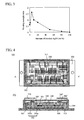
- Example 1 and Comparative Examples 1 and 2 The test results of the shearing strength for the bonding materials of Example 1 and Comparative Examples 1 and 2 are shown in FIG. 2 .
- Each bonding strength was represented as a relative ratio to the bonding strength of the specimen of Comparative Example 2 which was heated at 200°C for 60 minutes without application of pressure.
- the bonding strength ratio of Comparative Example 2 of which electrically conductive bonding material was made by blending 100 mass parts of silver flakes having an average particle size of about 1 ⁇ m, an average thickness of about 0.3 ⁇ m, and an aspect ratio of about 2.0, coated with 1.0 wt% stearic acid, into 20 mass parts of ethanol with a mortar for about 10 minutes, was low.
- Example 1 the bonding strength ratio of Example 1, of which electrically conductive bonding material was made by blending 0.9 g of silver flakes having an average particle size of about 1 ⁇ m, an average thickness of about 0.5 ⁇ m, and an aspect ratio of about 2.0, coated with 1.0 wt% stearic acid, 0.1 g of silver oxide (Ag 2 O) particles having an average particle size of about 2 ⁇ m, and 0.2 g of ethanol (made by Wako Pure Chemical Industries) as an organic solvent with a mortar for about one hour, was substantially improved.
- a relative strength ratio of 2.0 is achieved in the case of heating for 60 minutes. The advantageous effect of blending silver oxide into silver flakes on substantially improving bonding strength was thereby confirmed.
- Example 1 was compared to Comparative Examples 3 and 4.
- Comparative Example 3 nano-sized silver particles coated with octylamine disclosed in Japanese Patent Publication ( Kokai) No. 2008-161907 were used.
- Comparative Example 4 a blended bonding material of silver oxide particles and myristyl alcohol disclosed in JP Patent Publication (Kokai) No. 2008-178911 was made.
- Comparative Example 5 a bonding material was made by blending silver oxide (Ag 2 O) particles and myristyl alcohol in a ratio of 9 to 1 by weight and by braying the mixture with a mortar. A bonding strength test was made for these materials.
- the topside and downside test specimens for the measurement have a diameter of 5 mm and a thickness of 2 mm, and a diameter of 10 mm and a thickness of 5 mm, respectively.
- the surface of the specimens was plated with Ag.
- topside specimens were disposed on the respective bonding materials to heat at 200°C for bonding. Bonding strength was measured for the bonding portion which was only sheared.
- a bond tester SS-100KP maximum load of 100 kg
- the specimen was fractured with a shearing tool to measure the maximum load at fracture.
- the maximum load divided by the bonding area was defined as shearing strength.
- comparisons were made based on the bonding strength ratio.
- the electrically conductive bonding material of the present invention has a substantially improved bonding strength compared to the materials based on conventional bonding technology for achieving a metal bonding. It is understood that the electrically conductive bonding material of the present invention has excellent properties.
- Example 2 silver flakes having an average particle size of about 1 ⁇ m, an average thickness of about 0.5 ⁇ m, and an aspect ratio of about 2.0 were used.
- 100 mass parts of the specimens were blended into 20 mass parts of ethanol (made by Wako Pure Chemical Industries) as an organic solvent with a mortar for about 1 hour to make 1 g of the electrically conductive bonding materials, respectively. Subsequently, strength in shear was measured.
- the topside and downside test specimens for the measurement have a diameter of 5 mm and a thickness of 2 mm, and a diameter of 10 mm and a thickness of 5 mm, respectively.
- the surface of the specimens was plated with Ag.
- topside specimens were disposed on the bonding material to heat at 200°C for bonding. The heating time was 60 minutes.
- Each strength was represented as a relative ratio to the bonding strength of the specimen of Comparative Example 2 which was heated at 200°C for 60 minutes without application of pressure.
- the highest bonding strength was achieved in the case of a mixture having 5 wt% silver oxide (Ag 2 O) particles.
- the reason is that the proportion of stearic acid and silver oxide particles was most suitable for the redox. With excessive silver oxide, silver oxide remains, and with insufficient silver oxide, organic material remains in the circumference of silver particles. In these cases, the substantial improvement in bonding strength is not achieved.
- thermal conductivity W / mK Thermal diffusivity m 2 / s ⁇ Specific heat J / g ⁇ K ⁇ Density g / cm 3
- Thermal diffusivity (m 2 /s), density (g/cm 3 ), and specific heat (J/g ⁇ K), which are required to calculate the thermal conductivity, were measured with apparatus as described below. Thermal diffusivity was measured for specimens having a shape of 5 mm by 10 mm by 0.1 ⁇ m with PIT1 made by ULVAC SINKU-RIKO. Density was measured with SD-200L made by Alfa Mirage. Specific heat was measured with Q2000 made by TA Instrument. The thermal conductivity was calculated from these measured data. The results are shown in Table 2.
- Example 2 Each value represented in Table 2 is a relative ratio to the thermal conductivity of the specimen of Comparative Example 2 which was heated at 200°C for 60 minutes without application of pressure. Comparative Examples 1, 3 and 4 have lower thermal conductivities compared to Comparative Example 2. The results also correspond to the bonding strength. The reasons are that Comparative Example 1 contains a resin having a low thermal conductivity, and each of Comparative Examples 3 and 4 has a low density without application of pressure. On the other hand, Example 2 using the specimen having a blending ratio of silver flakes to silver oxide by weight of 90 to 10 had a higher thermal conductivity compared to Comparative Example 2. This resulted from more progressive sintering of the film formed at the same temperature, since the sintering temperature was reduced by blending silver oxide. As described above, the bonding material of Example 2 has advantages not only in bonding strength, but also in thermal conductivity.
- FIG. 4 shows a structure of a non-insulated semiconductor device of an Application Example of the present invention.
- FIG. 4 (A) is a top view
- FIG. 4 (B) is a cross-sectional view, taken along the line A-A' in FIG. 4 (A) .
- MOSFET semiconductor element
- a ceramic insulating substrate 302 are mounted on the ceramic insulating substrate 302 and a base member 303, respectively, an epoxy resin case 304, a bonding wire 305, and an epoxy resin lid 306 were disposed where the case was filled with silicone gel resin 307.
- the ceramic insulating substrate 302 on the base member 303 is bonded with a bonding layer 308 composed of the electrically conductive bonding material of Example 1, and the eight MOSFET elements 301 of Si on a copper plate 302a of the ceramic insulating substrate 302 is bonded with a bonding layer 309 composed of the electrically conductive bonding material of Example 1.
- the electrically conductive bonding material of Example 1 is initially applied onto the Ni-plated copper plate 302a of the ceramic insulating substrate 302 and the base member 303, respectively.
- the semiconductor element 301 and the ceramic insulating substrate 302 are disposed on the electrically conductive bonding material of Example 1 for connection. Bonding was performed by heating at about 150°C for 120 minutes in the air.
- a gate electrode, a emitter electrode and the like formed on each element 301 were wire-bonded by ultrasonic bonding to electrodes 302a and 302b formed on the insulating substrate and a terminal 310 previously attached to the epoxy resin case 304 with an Al wire 305 having a diameter of 300 ⁇ m.
- a thermistor element 311 for detecting temperature is composed of the bonding layer 309 bonded with the electrically conductive bonding material of Example 1 and electrode 302b is wire-bonded to the terminal 310 with the Al wire 305 having a diameter of 300 ⁇ m to connect with an exterior.
- Epoxy resin case 304 and base member 303 were fixed to each other with a silicone adhesive resin, which is not shown in the attached drawings.
- the epoxy resin lid 306 has pits 306' in fleshy portions and the terminal 310 has a hole 310' so that a screw (not shown in the attached drawings) for connecting an insulated semiconductor device 1000 with an external circuit can be mounted.
- the terminal 310 which is formed by punching a copper plate in a predetermined shape and then Ni-plated, is attached to the epoxy resin case 304.
- FIG. 5 shows a subassembly of an insulated semiconductor device shown in FIG. 4 .
- the ceramic substrate and the semiconductor element are mounted on the composite 303 as a base member.
- a mounting hole 303A is disposed in the circumference of the base member.
- the base member is composed of Cu.
- the surface of the base member is Ni-plated.
- the ceramic insulated substrate 302 is mounted on the base member 303 with the bonding layer bonded with the electrically conductive bonding material of Example 1.
- the MOSFET element 301 is mounted on the ceramic insulated substrate 302 with the bonding layer bonded with the electrically conductive bonding material of Example 1. On this occasion, bonding is performed in a thermostatic chamber heated at 250°C for 60 minutes in the air.
- FIG. 6 is an enlarged schematic cross-sectional view of a mounting part of the MOSFET element in FIG. 5 before bonding.
- the electrically conductive bonding material of Example 1 can be used in the bonding layer.
- a water-shedding film 322 is applied on the base member 303 corresponding to the region of mounting the ceramic insulating substrate 302.
- a water-shedding film 321 is applied on the ceramic insulating substrate 302 corresponding to the region of mounting the semiconductor element 301 so that the applied paste is prevented from flowing outward.
- Application Example 2 relates to an insulated semiconductor device as a highfrequency power amplifier device used in a transmitter for a cellular phone and the like.
- the structure of the insulated semiconductor device having a size of 10.5 mm by 4 mm by 1.3 mm is given as follows.
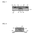
- FIG. 7 is a schematic cross-sectional view of the insulated semiconductor device of Application Example 2.
- Chip parts including a MOSFET element 1 having a size of 2.4 mm by 1.8 mm by 0.24 mm, a chip resistor 101 (about 7 ppm/°C), and a chip capacitor 102 (about 11.5 ppm/°C) are mounted on a multi-layer glass ceramic substrate having a size of 10.5 mm by 4 mm by 0.5 mm, a 3-layer interconnection, a coefficient of thermal expansion of 6.2 ppm/°C, a thermal conductivity of 2.5 W/m.K, a bending strength of 0.25 GPa, a Young's modulus of 110 GPa, and a permittivity of 5.6 (1 MHz), as a base member 100.
- An intermediate metal member 103 composed of, for example, Cu-Cu 2 O composite is disposed between the MOSFET element 1 and the multi-layer glass ceramic substrate 100.
- a thick film internal interconnecting layer (Ag-1 wt% Pt, a thickness of 15 ⁇ m), a thick film through-hole conductor (Ag-1 wt% Pt, a diameter of 140 ⁇ m) for an electrical connection between the multi-layer interconnections, and a thick film thermal via (Ag-1 wt% Pt, a diameter of 140 ⁇ m) for heat dissipation path are disposed in the multi layer glass ceramic substrate 100.
- a thick film interconnecting pattern 104 (Ag-1 wt% Pt, a thickness of 15 ⁇ m) is also disposed on a main plane of the multi layer glass ceramic substrate 100. Chip parts including the chip resistor 101 and the chip capacitor 102 are mounted on this thick film interconnecting pattern 104.
- the electrically conductive bonding material of Example 1 is prepared by blending the equivalent amount of decanol as the organic solvent instead of ethanol with a mortar for 10 minutes to form a paste. Then, the paste is applied onto the thick film interconnecting pattern. By heating the paste at 200°C for 30 minutes in a thermostatic chamber substituted by hydrogen, a sintered silver layer 105 for electrically conductive bonding of the chip parts is formed.
- the MOSFET element (Si, 3.5 ppm/°C) 1 is mounted in a recess disposed on a main plane of the multi layer glass ceramic substrate 100 through an intermediate metal member 103.
- the mounting was performed in vacuum of 10 -3 .
- the intermediate metal member 103 has a size of 2.8 mm by 2.2 mm by 0.2 mm.
- Both of the sintered silver layer 105 for connecting the MOSFET element 1 and the intermediate metal member 103, and the bonding layer 106 for connecting the intermediate metal member 103 and the multi layer glass ceramic substrate 100 are bonded layers made from the electrically conductive bonding material of Example 1 in paste form prepared by blending the equivalent amount of decanol as the organic solvent instead of ethanol with a mortar for 10 minutes to form the paste.
- a clip-type connecting terminal 107 composed of Cu is bonded with the electrically conductive bonding material of Example 1 for connecting a MOSFET element 1 and a predetermined portion of the thin film interconnecting pattern 104. On this occasion, the bonding was performed by heating at 200°C for 30 minutes in a thermostatic chamber substituted by hydrogen.
- a thick film external electrode layer 104' (Ag-1 wt% Pt, a thickness of 15 ⁇ m) is disposed.
- the thick film external electrode layer 104' is electrically connected with the thick film interconnecting pattern 104 through an internal interconnecting layer and a through-hole interconnection disposed in the multi layer glass ceramic substrate 100.
- an epoxy resin layer 108 is disposed to seal the mounted chip parts.
- Application Example 3 relates to a non-insulated semiconductor device in which a composite is applied as a lead frame of a mini-mold type transistor.
- FIG. 8 is a cross-sectional schematic view of a mini-mold type non-insulated semiconductor device of Application 3.
- a transistor element having a size of 1 mm by 1 mm by 0.3 mm composed of Si as a semiconductor element 1 is bonded with a sintered silver layer 601 by applying the electrically conductive bonding material of Example 1 on a lead frame 600 having a thickness of 0.3 mm composed of, for example, a composite of Cu-Cu 2 O and by heating at 200°C for 60 minutes in a thermostatic chamber substituted by nitrogen.
- a collector of the transistor element 1 is also disposed on the side bonded with the electrically conductive bonding material of Example 1.
- An emitter and a base are disposed on the opposite side of the side bonded with the electrically conductive bonding material of Example 1 and bonded to a clip type terminal 602 derived from the transistor element 1 with the electrically conductive bonded material applied to the lead frame 600 by heating in the same way at 200°C for 60 minutes in a thermostatic chamber substituted by nitrogen.
- the main portion of the mounted transistor element 1 with the clip type terminal 602 is covered with an epoxy resin 603 by transfer molding.
- the lead frame 600 is cut off after completion of molding of the epoxy resin 603 for functioning as individual terminals.
Landscapes
- Chemical & Material Sciences (AREA)
- Physics & Mathematics (AREA)
- Dispersion Chemistry (AREA)
- Spectroscopy & Molecular Physics (AREA)
- Conductive Materials (AREA)
- Powder Metallurgy (AREA)
- Adhesives Or Adhesive Processes (AREA)
- Engineering & Computer Science (AREA)
- Die Bonding (AREA)
- Ceramic Engineering (AREA)
- Materials Engineering (AREA)
- Mechanical Engineering (AREA)
- Metallurgy (AREA)
- Organic Chemistry (AREA)
Abstract
Description
- The present invention relates to an electrically conductive bonding material, a method of bonding with the same, and a semiconductor device bonded with the same. For example, the invention relates to a bonding material and a method of bonding used in a semiconductor module.
- In a non-insulated semiconductor device used in inverters and the like as a power semiconductor device, an anchoring member for attaching a semiconductor element functions as an electrode of the semiconductor device. For example, in a semiconductor device having a power transistor mounted on an anchoring member with a Sn-Pb solder, the anchoring member (base member) is a collector electrode of the power transistor. In operating the semiconductor device, the collector electrode carries an electric current of several or more amperes, resulting in heating the transistor chip. In order to prevent property destabilization or service life reduction due to the heat generation, a good heat dissipation capacity and a long-term reliability (heat resistance) have to be secured in the soldered portion. A material with high heat dissipation is required for securing the heat resistance and heat dissipation performance in a soldered portion.
- Similarly, in an insulated semiconductor device, for safe and stable operation of a semiconductor element, developed heat during operating period of a semiconductor device needs to be efficiently dissipated to the exterior of the semiconductor device and reliability of bonding in a soldered portion needs to be secured. For example, in an environment, such as an automotive engine compartment, frequently exposed to high temperatures, the reliability of a bonding portion must be sufficiently high.
- Although a bonding material having a high melting point may be used for enhancing heat resistance of a bonding portion, bonding temperature is inevitably raised in this case. A high bonding temperature may cause an anchoring member to get damaged by heat or may cause a warp of an entire semiconductor device due to a difference in stress between a substrate and the anchoring member during a cooling period after bonding. That means heat resistance of a bonding material needs to be enhanced while bonding temperature needs to be lowered.
- For example, as described in
JP Patent Publication (Kokai) No. 2003-309352 - In
JP Patent Publication (Kokai) No. 2005-129303 - It is known that a metal particle having a particle size of not greater than 100 nm with few constituent atoms has a sharply increased ratio of surface area to volume of the particle, so that the sintering temperature is substantially reduced compared to that of a bulk form (resulting in increased sintering performance or increased surface energy). For example,
JP Patent Publication No. 2004-107728 - Unfortunately, heat dissipation capacity and bonding reliability achieved by the bonding materials (electrically conductive adhesives) described in
JP Patent Publication (Kokai) No. 2003-309352 JP Patent Publication (Kokai) No. 2005-129303 - Since the bonding material disclosed in
JP Patent Publication No. 2004-107728 - The present invention has been made taking such circumstance into consideration and provides an electrically conductive bonding material that has high heat resistance after bonding, enables a metal bonding at a bonding interface at a lower temperature as compared to an electrically conductive bonding materials containing a resin, and enables bonding in the absence of pressure not requiring application of pressure during a bonding process; a bonding method with the same; and a semiconductor device bonded with the same.
- In order to solve the problems as described above, in the present invention, a metal bonding in a bonding portion is produced with silver powder (particles) and silver oxide powder (particles) having a particle size of 0.1 µm to 100 µm (micro particles), which have not been taken into consideration heretofore. In the present invention, simplification of a bonding process is achieved by avoiding use of a resin (reducing a content of organic material), thereby allowing elimination of pressure application during the bonding process.
- Although use of lead-free solder is preferred, no alternative material is available for high-temperature soldering. Since hierarchical soldering is indispensable in packaging technology, an alternative material for high-temperature soldering is desired. Accordingly, the bonding technology of the present invention is expected to provide the alternative material for high-temperature soldering.
- The present inventors found that an electrically conductive bonding material comprising (A) silver powder, (B) silver oxide powder, and (C) a dispersant composed of an organic material containing not more than 30 carbon atoms as essential components, wherein a total amount of the (A) silver powder, the (B) silver oxide powder, and the (C) dispersant composed of an organic material containing not more than 30 carbon atoms is in a range of 99.0% to 100% by weight of the whole electrically conductive bonding material, enables silver particles to start sintering at a low temperature not higher than 200°C and enables bonding without application of pressure. On this occasion, the blended silver oxide particles are reduced to silver by a redox reaction with the dispersant composed of organic material at a temperature not higher than 150°C so as to cause fusion, which promotes sintering at a temperature not higher than 200°C. Thus, bonding strength is further improved compared to the case in which silver particles are used alone. In addition, the present inventors found that the silver particles and the silver reduced from the silver oxide used as the bonding material enable bonding to an electrode to be connected without using a resin binder.
- The electrically conductive bonding material of the present invention comprises silver particles, silver oxides particles, and a dispersant composed of an organic material containing not more than 30 carbon atoms as essential components, wherein a total amount of the silver particles, the silver oxide particles, and the dispersant is in a range of 99.0% to 100% by weight. The silver particles and the silver oxide particles have particle sizes of 0.1 µm to 100 µm (both inclusive). The silver particles may be in flake form. At least one of the silver particles and the silver oxide particles are coated with a dispersant. Preferably, an amount of the silver oxide particles is not more than an amount of the dispersant. The silver particles and the silver oxide particles are in the ratio of 100 mass parts of the silver particles to 0.01 mass parts to 100 mass parts (both inclusive) of the silver oxide particles.
- In another embodiment, the electrically conductive bonding material comprises silver particles, silver oxides particles, a dispersant composed of an organic material containing not more than 30 carbon atoms, and an organic solvent having a boiling point of not higher than 350°C as essential components, wherein when a total amount of the silver particles, the silver oxide particles, the dispersant, and the organic solvent is 100 mass parts, an amount of the organic solvent is not more than 90 mass parts, and a total amount of the silver particles, the silver oxide particles, the dispersant, and the organic solvent is in a range of 99.0% to 100% by weight in paste form.
- In another embodiment, the electrically conductive bonding material comprises silver particles, silver oxides particles, a dispersant composed of organic material containing not more than 30 carbon atoms, and metal particles of other than silver as essential components, wherein the total amount of the silver particles, the silver oxide particles, the dispersant, and the metal particles of other than silver is 99.0% to 100% by weight.
- In yet another embodiment, the electrically conductive bonding material comprises silver particles, silver oxides particles, a dispersant composed of an organic material containing not more than 30 carbon atoms, an organic solvent having a boiling point of not higher than 350°C, and metal particles of other than silver as essential components, wherein when a total amount of the silver particles, the silver oxide particles, the dispersant, the organic solvent, the organic solvent, and the metal particles is 100 mass parts, an amount of the organic solvent is not more than 90 mass parts, and a total amount of the silver particles, the silver oxide particles, the dispersant, the organic solvent, and the metal particles of other than silver is in a range of 99.0% to 100% by weight. The bonding material is in paste form.
- The semiconductor device of the present invention is bonded by any one of the electrically conductive bonding materials described above, and the bonding portion is composed of a metal part alone with a porosity of higher than 0.1% and lower than 90%.
- In the method of bonding of the present invention, any one of the electrically conductive bonding material described above is disposed between an electrode of a semiconductor element and a metal member and sintered by heating in an atmosphere of hydrogen, nitrogen, or argon, so that the electrode of the semiconductor element and the metal member are metal bonded.
- The further features of the present invention will be apparent in the description of preferred embodiments of the present invention and the accompanying drawings.
- The present invention can provide a bonding material and a method of bonding for enabling a metal bonding at a bonding interface at a lower temperature compared to a bonding material with metal particles having an average particle size of not greater than 100 nm. Since a resin binder is not used, a bonding process without application of pressure can be provided for producing a bonding portion having high heat resistance and high heat dissipation after bonding.
-
-
FIG. 1 is a schematic view of a bonding process with silver flakes and silver oxide particles. -
FIG. 2 is a graph showing changes in bonding strength induced by adding silver oxide particles to silver flakes. -
FIG. 3 is a graph showing an effect of a proportion of the silver oxide added to the silver flakes. -
FIG. 4 shows a structure of a non-insulated semiconductor device of an example of the present invention. -
FIG. 5 shows a subassembly of an insulated semiconductor device of the present invention. -
FIG. 6 is an enlarged schematic view of a bonding part of a semiconductor element and a substrate. -
FIG. 7 is a cross-sectional schematic view of an insulated semiconductor device of the example. -
FIG. 8 is a cross-sectional schematic view of a mini-mold type non-insulated semiconductor device of the example. -
- 201 Member to be bonded
- 202 Ag Flake
- 203 Ag2O
- 205 Sintered silver layer
- 301 Semiconductor element
- 302 Ceramic insulating substrate
- 302a Copper plate
- 303 Base member
- 304 Epoxy resin case
- 305 Bonding wire
- 306 Epoxy resin lid
- 307 Silicone gel resin
- 308, 309 Bonding layer
- 310 Terminal
- Specific embodiments of the present invention will be now described. Subsequently, Examples and Application Examples will be described.
Composition of the bonding material
The present invention relates to an electrically conductive bonding material comprising (A) silver powder, (B) silver oxide powder, and (C) a dispersant composed of an organic material containing not more than 30 carbon atoms as essential components. In an electrically conductive bonding material with such a composition, a total amount of (A) silver powder, (B) silver oxide powder, and (C) the dispersant composed of an organic material containing not more than 30 carbon atoms is in a range of 99.0% to 100% by weight. In other words, a conventional resin is not contained in the composition. During bonding, the electrically conductive bonding material is heated to sinter the silver particles and the silver oxide particles, so that a metal bonding is formed. Blending silver powder with silver oxide gives a dispersant and silver oxide a redox reaction during bonding at a temperature not higher than 150°C. Since the reaction promotes sintering of the silver powder, bonding strength at low temperature can be improved. - Since the bonding mechanism effected by the bonding material of the present invention is based on a metal bonding without a resin, the bonding portion can have high heat resistance and high heat dissipation capacity after bonding. Since such a metal bonding can be produced at a low temperature, the bonding material of the present invention can be applied to, for example, bonding an electrode disposed on an active area of a semiconductor element and a mounting part of an interconnecting substrate for mounting the device. In addition, since the bonding layer after bonding has higher a heat resistance compared to the conventional solder material, no melting problem in a portion mounting a semiconductor element occurs in a thermal process such as secondary packaging. A downsized and highly-reliable semiconductor device can be thereby produced.
- Furthermore, the bonding material can substantially improve bonding strength without application of pressure compared to a material of metal nanoparticles having an average particle size of not greater than 100 nm. The metal bonding without application of pressure, which was difficult to achieve by conventional technology, can substantially simplify the bonding process due to omission of the process for application of pressure during bonding. Since no pressure is applied during bonding, damage to a semiconductor chip during bonding can be substantially reduced.
- The silver particles and the silver oxide particles for use have an average particle size of not smaller than 0.1 µm and not greater than 100 µm. Metal particles having an average particle size of greater than 100 µm have low dispersibility in the electrically conductive bonding material, so that a dense bonding layer cannot be produced. The average particle size is set at not smaller than 0.1 µm, because metal particles having an average particle size of smaller than 0.1 µm need to have their circumference coated with a large amount of organic material in order to prevent the particles from attaching each other in a normal condition and in the cases that such particles are used for bonding, volume contraction occurs while removing the organic material, so that bonding without application of pressure becomes difficult.
- Examples of the silver oxide particles include Ag2O and AgO. A bonding material composed of at least one or two metals may be used. Metal oxides composed of gold oxide and copper oxide may be added concurrently with silver oxide particles for use.
- The particles of silver oxide and silver for use may be in form of flake. In example to be described, as shown in
FIG. 1 , silver particles alone is in form of flake. An average particle size of the flake is preferably not greater than 100 µm, more preferably not greater than 50 µm, and most preferably not greater than 10 µm. The preferred lower limit is greater than or equal to 0.1 µm. Flakes having an average particle size of greater than 100 µm may cause clogging in mesh for screen printing or reduce stability of storage paste by sedimentation of the particles in form of flake. Meanwhile, particles in form of flake having an average particle size of smaller than 0.1 µm may not be filled enough due to high viscosity of the paste. - The particles in form of flake have an average thickness of, preferably not greater than 5.0 µm and more preferably not greater than 1 µm. The lower limit is not specifically limited and preferably greater than or equal to 0.1 µm. Flakes having an average thickness of greater than 2.0 µm may have reduced electrical conductivity due to a reduced aspect ratio.
- An aspect ratio of the particles in form of flake is preferably greater than 1.0 and more preferably 2 or greater. An upper limit is not specifically determined, preferably not greater than 200, and more preferably not greater than 150.
- Shapes of the particles are not limited to a sphere or a flake as described above. A tetrahedron, an octahedron, a rod, and a fiber may be used. Particles in form of flake can make a surface contact each other so as to increase the contact area.
- Blending ratio of silver particles to silver oxide particles
- Preferably, a blending ratio of silver oxide particles to silver particles is in a range of 0.01 mass parts to 100 mass parts (both inclusive) of silver oxide particles relative to 100 mass parts (% by weight) of silver particles. The blending ratio is set at not smaller than 0.01 mass parts, because the quantities of silver reduced from silver oxide is not enough for the effect of fusing silver at a low temperature with an amount of silver oxide of less than 0.01 mass parts. The blending ratio is set at not greater than 100 mass parts, because the increased portion of volume contraction in a bonding layer causes bonding strength to be reduced with an amount of silver oxide of more than 100 mass parts. Considering bonding strength, a preferred ratio of silver oxide is about 40% by weight (see
FIG. 3 ). - Examples of a dispersant (and also reducing agent for silver oxide) composed of an organic material containing not more than 30 carbon atoms include mixtures of at least one constituent selected from alcohols, carboxylic acids, and amines. The mixtures coat the circumference of the blended metal particles with an organic material to improve dispersibility of the particles in an organic solvent. For example, in cases that stearic acid is used as a dispersant for preventing silver particles from attaching to each other, stearic acid is removed from the silver particles by reducing reaction of silver oxide and stearic acid attaching to silver particles at a temperature of 140°C to 150°C. With an excessive by high blending ratio of silver oxide to stearic acid, silver oxide remains in the bonding material due to the insufficient reducing reaction. In this case, bonding strength is not improved. Consequently, a blending ratio of silver oxide to the dispersant is preferably at most 1:1.
- The number of carbon atoms is limited to not more than 30, since an excessive number of carbon atoms cause the boiling point of dispersant to rise and the remaining dispersant in the bonding portion after heating (e.g. 200°C) during bonding may cause problems in bonding strength and reliability.
- Examples of available compounds comprising an alcohol group include alkyl alcohol such as ethanol, propanol, butyl alcohol, pentyl alcohol, hexyl alcohol, heptyl alcohol, octyl alcohol, nonyl alcohol, decyl alcohol, undecyl alcohol,
dodecyl alcoho 1, tridecyl alcohol, tetradecyl alcohol, pentadecyl alcohol, hexadecyl alcohol, heptadecyl alcohol, octadecyl alcohol, nonadecyl alcohol, and icosyl alcohol. In addition, without limitation to primary alcohols, secondary alcohols, tertiary alcohols, alkane diol, or cyclic alcohol compounds may be used. Furthermore, ethylene glycol, triethylene glycol or compounds having many alcohol groups such as citric acid, ascorbic acid, and glucose may be used. - Examples of available compounds containing carboxylic acid include alkylcarboxylic acids such as butanoic acid, pentanoic acid, hexanoic acid, heptanoic acid, octanoic acid, nonanoic acid, decanoic acid, undecanoic acid, dodecanoic acid, tridecanoic acid, tetradecanoic acid, pentadecanoic acid, hexadecanoic acid, heptadecanoic acid, octadecanoic acid, nonadecane acid, icosanoic acid, and oleic acid. Similarly to the alcohol groups as described above, in addition, without limitation to primary alcohols, secondary carboxylic acids, tertiary carboxylic acids, dicarboxylic acids or carboxylic compounds having a cyclic structure may be used.
- Furthermore, examples of available compounds containing an amino group include alkylamines such as butylamine, pentylamine, hexylamine, heptylamine, octylamine, nonylamine, decylamine, undecylamine, dodecylamine, tridecylamin, tetradecylamine, pentadecylamine, hexadecylamine, heptadecylamine, octadecylamine, nonadecylamine, and icodecylamine. The compounds having an amino group may have a branching structure. Example of such compounds include 2-ethyl hexylamine and 1, 5-dimethylhexylamine. In addition, without limitation to primary amines, secondary amines or tertiary amines may be used. Furthermore, such an organic material may have a cyclic structure.
- The dispersants for use are not limited to organic materials including alcohols, carboxylic acids, and amines. Organic materials containing an aldehyde group, an ester group, a sulfanyl group, or a ketone group may be used. Coating here means that functional groups in the organic material is connected with silver or silver oxide to have a role for preventing aggregation. Such a structure is distinguished by infrared spectrometry. In cases that carboxyl acid coats the circumference of silver powder or silver oxide, a carbonyl salt is formed.
- According to a spectral analysis by infrared spectrometry of silver with the addition of a dispersant, weak peaks appear in the vicinity of 1520 cm-1 and in the vicinity of 1420 cm-1. These peaks cannot be observed in cases that a connection with silver is not present. Consequently, an organic material coating the particles can be identified by infrared spectrometry. Determinable organic materials are not limited to carboxyl acid. Any organic materials having functional groups can be identified.
- An amount of the dispersant for use may be in a range of 0.01 mass parts to 20 mass parts relative to 100 mass parts of a total of silver particles and silver oxide particles. With an amount of dispersant of less than 0.01 mass parts, the low dispersibility of the silver particles and the silver oxide particles causes secondary aggregation, so that uniform application to the bonding portion becomes difficult and bonding without application of pressure is precluded. The amount of the dispersant is set at not more than 20 mass parts, because silver particles are blocked from fusing to each other so that the bonding strength is substantially reduced with an amount of dispersant of more than 20 mass parts.
- In an electrically conductive bonding material having silver particles, silver oxide particles, and a dispersant composed of not more than 30 carbon atoms, the total amount of the mixture of these constituents for use is in a range of 99.0% to 100% by weight. The reason for the range is that a resin binder blended in the mixture substantially inhibits sintering between silver particles so as to significantly reduce bonding strength. The limit is set at 99.0%, taking the purity of silver available for use usually into consideration, because silver free of impurities is rare.
- Particles other than silver particles with relatively large particle size having an average particle size of 0.1 µm to 100 µm can be blended in the bonding material for use. The reason for the availability is that the silver particles and the silver oxide particles blended in the electrically conductive bonding material have a function to sinter the other metal particles having an average particle size of 0.1 µm to 100 µm to each other. Examples of such metal particles include gold and copper. Other than the metals described above, at least one metal of, or an alloy of metals of, platinum, palladium, rhodium, osmium, ruthenium, iridium, iron, tin, zinc, cobalt, nickel, chrome, titanium, tantalum, tungsten, indium, silicon, aluminum can be used.
- Alternatively, metal particles having an average particle size of not greater than 100 nm may be blended in advance in the bonding material. Metal species for such particles include gold, silver, and copper or oxides of these metals, i.e. gold oxide, silver oxide, and copper oxide. Other than the metals described above, at least one metal of, or an alloy of metals of, platinum, palladium, rhodium, osmium, ruthenium, iridium, iron, tin, zinc, cobalt, nickel, chrome, titanium, tantalum, tungsten, indium, silicon, aluminum can be used. These may be blended for use in a range not to substantially degrade the properties of the electrically conductive bonding material of the present invention.
- In cases that other metals are blended in the bonding material, however, a resin is not allowed to be contained due to the reason as described above.
- Although the electrically conductive bonding material for use in the present embodiment may be composed only of silver particles, silver oxide particles, and a dispersant (plus other metal particles), a solvent having a boiling point of not higher than 350°C may be added for use of the bonding material in paste form. Examples of such a solvent include alcohols. The upper limit of a boiling temperature is set at not higher than 350°C, because a solvent having an excessively high boiling point needs long time for evaporation during bonding at a target temperature of 200°C to 250°C and the limit of 350°C is therefore considered appropriate. Organic materials such as alcohols having a boiling point of higher than 350°C are not definitely unsuitable, however. Such organic materials may be used depending on intended application.
- Examples of available organic materials containing an alcohol group include methanol, ethanol, propanol, butyl alcohol, pentyl alcohol, hexyl alcohol, heptyl alcohol, octyl alcohol, nonyl alcohol, decyl alcohol, undecyl alcohol, dodecyl alcohol, tridecyl alcohol, tetradecyl alcohol, pentadecyl alcohol, hexadecyl alcohol, heptadecyl alcohol, octadecyl alcohol, nonadecyl alcohol, and icocyl alcohol. In addition, glycols such as diethylene glycol, ethylene glycol, and triethylene glycol can be used. In addition, without limitation to primary alcohols, secondary alcohols, tertiary alcohols, alkanediol, or cyclic alcohol compounds may be used. Alternatively, terpineol, ethylene glycol, triethylene glycol or compounds having many alcohol groups such as citric acid, ascorbic acid, and glucose may be used. The preferred compound is selected from secondary alcohols or tertiary alcohols. The reason is that primary alcohols blended with silver oxide reduce a portion of the surface of silver oxide to concurrently produce salt and precipitated silver after one day, so that stability of storage silver oxide is reduced. With secondary alcohols or tertiary alcohols, no reaction occurs for producing the salt on the surface of silver oxide, and the stability of storage is excellent. Most preferably, glycol solvent is used due to availability at low price and low toxic potential for human body. Furthermore, since an alcohol solvent may function as not only a solvent but also a reducing agent for silver oxide, the amount can be properly adjusted for reducing a certain amount of silver oxide.
- Alternatively, instead of the organic materials having an alcohol group as described above, carboxylic acid, amine, or an organic material having an aldehyde group, an ester group, a sulfanyl group, or a ketone group can be used. Furthermore, toluene or an organic material composed of hydrocarbon alone having no functional group as described above such as hexane and cyclohexane may be used. As described above, an organic solvent having a boiling point of not higher than 350°C may be used and more than one of such organic solvents may be blended for use. The organic material having a boiling point of not higher than 350°C is defined here as an organic material which reduces weight by 99 wt% up to 350°C in nitrogen atmosphere at 10°C/min in measurement with a thermogravity analyzer such as TG/DTA6200 made by Seiko Instruments and TGA-50 made by Shimadzu.
- The amount of the organic solvent to be blended may be preferably not higher than 90% by weight, or more preferably not higher than 50% by weight relative to 100% by weight of the electrically conductive bonding material of the present invention. The mixture may be agitated with a mortar, a kneader, a vibratory ball mill, a roller mill, or a planet ball mill.
- The electrically conductive bonding material in paste form is applied by various methods. For example, the electrically conductive bonding material is ejected through a fine nozzle for applying to an electrode or a connecting portion of an electronic component by ink jet method; the material is applied only to a necessary part with a metal mask having an aperture corresponding to the part to be coated or a mesh mask; the material is applied to a necessary part with a dispenser; and the material is applied to a water-shedding resin containing silicone or fluorine with a metal mask having an aperture corresponding to the part to be coated or a mesh mask. These methods of application can be combined depending on the area and shape of the electrode to be bonded. Alternatively, pressure is applied on the electrically conductive bonding material to form into sheet for use in bonding.
- For bonding with the electrically conductive bonding material of the present invention, heating during bonding is indispensable in order to achieve sintering silver particles to each other, reducing silver oxide, and forming a metal bonding with electrode surface. In the preferred heating conditions for the bonding, temperature ranges from 40°C to 350°C (both inclusive) during a time period of 1 second to 180 minutes (both inclusive).
- With conventional metal particles having an average particle size of not greater than 100 nm, application of pressure is required during bonding since desorption of an organic material causes volume contraction of the metal particles. Meanwhile, in the present invention, a metal bonding at the bonding interface can be achieved without application of pressure. The bonding process can be thereby simplified. However, pressure may be applied if needed for improving the bonding strength.
- The reason for the lower limit of heating temperature is that a heating temperature of lower than 40°C causes insufficient sintering of silver particles and insufficient reduction of silver oxide so that bonding cannot be achieved.
- The reason for the upper limit of heating period is that a heating period of longer than 180 minutes makes difficulty in high-volume manufacturing due to the lengthy time required for making one product.
- Atmosphere for bonding is not limited to air. Reducing atmosphere such as hydrogen or inert atmosphere such as nitrogen and argon can be used. Bonding in such atmosphere can ease the problem of oxidation of an electronic component in air.
- The bonding portion of an semiconductor device bonded with the electrically conductive bonding material of the present invention comprising (A) silver particles, (B) silver oxide, and (C) dispersant composed of an organic material containing not more than 30 carbon atoms as essential components, a total amount of (A) silver powder, (B) silver oxide powder, and (C) dispersant composed of an organic material containing not more than 30 carbon atoms being in a range of 99.0% to 100% by weight, is formed with the particles having shapes remaining intact, since no pressure is applied during bonding.
- Consequently, a void is inevitably present in the bonding layer. In a cross-sectional view of the bonding layer, the porosity (i.e. void area divided by bonding layer area) is in a range of 0.1% to 99.9%. The preferable porosity is not higher than 90%. Due to the presence of voids, the bonding layer has a lower density and a lower elastic modulus compared to a bonding layer of bulk silver. As a result, stress loading to a chip is reduced, so that long-term reliability of the bonding portion is improved.
- Examples and applications will be described below with reference to attached drawings.
- In Example 1, 0.9 g of silver flakes having an average particle size of about 1 µm, an average thickness of about 0.5 µm, and an aspect ratio of about 2.0, coated with 1.0 wt% stearic acid, 0.1 g of silver oxide (Ag2O) particles having an average particle size of about 2 µm, and 0.2 g of ethanol (made by Wako Pure Chemical Industries) as an organic solvent were used. These were blended with a mortar for about one hour to make an electrically conductive bonding material.
- As Comparative Example 1, a conventional silver paste which is available in the market was used. As Comparative Example 2, an electrically conductive bonding material was made by blending 100 mass parts of silver flakes having an average particle size of about 1 µm, an average thickness of about 0.3 µm, and an aspect ratio of about 2.0, coated with 1.0 wt% stearic acid, into 20 mass parts of ethanol with a mortar for about 10 minutes.
- Subsequently, after bonding was performed with the electrically conductive bonding materials of Example 1 and Comparative Examples 1 and 2, strength in shear was measured. The topside and downside test specimens for the measurement have a diameter of 5 mm and a thickness of 2 mm, and a diameter of 10 mm and a thickness of 5 mm, respectively. The surface of the specimens was plated with Ag. After the electrically conductive bonding materials of Example 1 and Comparative Examples 1 and 2 were applied onto the respective downside specimens, the respective topside specimens were disposed on the bonding material to heat at 200°C for bonding. The heating time was 5, 15, 30, and 60 minutes as shown in Table 1.

- As shown in
FIG. 1 , particles of the electrically conductive bonding material disposed betweenmembers 201 to be bonded are sintered to each other by heating, so that asintered silver layer 205 is formed. On this occasion, a metal bonding is achieved at the bonding interface between thesintered silver layer 205 and the bondedmember 201. Subsequently, bonding strength of the specimens bonded with the bonding material was measured under pure shear stress conditions. For the shearing test, a bond tester SS-100KP (maximum load of 100 kg) made by Seishin Trading was used. At a shearing speed of 30 mm/min, the specimen was fractured with a shearing tool to measure the maximum load at fracture. The maximum load divided by the bonding area was defined as shearing strength. - The test results of the shearing strength for the bonding materials of Example 1 and Comparative Examples 1 and 2 are shown in
FIG. 2 . Each bonding strength was represented as a relative ratio to the bonding strength of the specimen of Comparative Example 2 which was heated at 200°C for 60 minutes without application of pressure. The bonding strength ratio of Comparative Example 2, of which electrically conductive bonding material was made by blending 100 mass parts of silver flakes having an average particle size of about 1 µm, an average thickness of about 0.3 µm, and an aspect ratio of about 2.0, coated with 1.0 wt% stearic acid, into 20 mass parts of ethanol with a mortar for about 10 minutes, was low. On the other hand, the bonding strength ratio of Example 1, of which electrically conductive bonding material was made by blending 0.9 g of silver flakes having an average particle size of about 1 µm, an average thickness of about 0.5 µm, and an aspect ratio of about 2.0, coated with 1.0 wt% stearic acid, 0.1 g of silver oxide (Ag2O) particles having an average particle size of about 2 µm, and 0.2 g of ethanol (made by Wako Pure Chemical Industries) as an organic solvent with a mortar for about one hour, was substantially improved. A relative strength ratio of 2.0 is achieved in the case of heating for 60 minutes. The advantageous effect of blending silver oxide into silver flakes on substantially improving bonding strength was thereby confirmed. - Then, Example 1 was compared to Comparative Examples 3 and 4. In Comparative Example 3, nano-sized silver particles coated with octylamine disclosed in Japanese Patent Publication (
Kokai) No. 2008-161907 JP Patent Publication (Kokai) No. 2008-178911 - In Example 2, silver flakes having an average particle size of about 1 µm, an average thickness of about 0.5 µm, and an aspect ratio of about 2.0 were used. The specimens composed of silver flakes coated with 1.0 wt% stearic acid and silver oxide (Ag2O) particles having an average particle size of about 2 µm in a different blended ratio by weight of 95 to 5, 90 to 10, 80 to 20, or 50 to 50 were made. Furthermore, 100 mass parts of the specimens were blended into 20 mass parts of ethanol (made by Wako Pure Chemical Industries) as an organic solvent with a mortar for about 1 hour to make 1 g of the electrically conductive bonding materials, respectively. Subsequently, strength in shear was measured. The topside and downside test specimens for the measurement have a diameter of 5 mm and a thickness of 2 mm, and a diameter of 10 mm and a thickness of 5 mm, respectively. The surface of the specimens was plated with Ag. After the electrically conductive bonding materials of Example 1 and Comparative Examples 1 and 2 were applied onto the respective downside specimens, topside specimens were disposed on the bonding material to heat at 200°C for bonding. The heating time was 60 minutes. Each strength was represented as a relative ratio to the bonding strength of the specimen of Comparative Example 2 which was heated at 200°C for 60 minutes without application of pressure.
- As shown in
FIG. 3 , the highest bonding strength was achieved in the case of a mixture having 5 wt% silver oxide (Ag2O) particles. The reason is that the proportion of stearic acid and silver oxide particles was most suitable for the redox. With excessive silver oxide, silver oxide remains, and with insufficient silver oxide, organic material remains in the circumference of silver particles. In these cases, the substantial improvement in bonding strength is not achieved. - Subsequently, the results of thermal conductivity measurement of Example 2, Comparative Examples 1 to 4 were compared. The thermal conductivity is defined by equation (1).

- Thermal diffusivity (m2/s), density (g/cm3), and specific heat (J/g·K), which are required to calculate the thermal conductivity, were measured with apparatus as described below. Thermal diffusivity was measured for specimens having a shape of 5 mm by 10 mm by 0.1 µm with PIT1 made by ULVAC SINKU-RIKO. Density was measured with SD-200L made by Alfa Mirage. Specific heat was measured with Q2000 made by TA Instrument. The thermal conductivity was calculated from these measured data. The results are shown in Table 2.
- Each value represented in Table 2 is a relative ratio to the thermal conductivity of the specimen of Comparative Example 2 which was heated at 200°C for 60 minutes without application of pressure. Comparative Examples 1, 3 and 4 have lower thermal conductivities compared to Comparative Example 2. The results also correspond to the bonding strength. The reasons are that Comparative Example 1 contains a resin having a low thermal conductivity, and each of Comparative Examples 3 and 4 has a low density without application of pressure. On the other hand, Example 2 using the specimen having a blending ratio of silver flakes to silver oxide by weight of 90 to 10 had a higher thermal conductivity compared to Comparative Example 2. This resulted from more progressive sintering of the film formed at the same temperature, since the sintering temperature was reduced by blending silver oxide. As described above, the bonding material of Example 2 has advantages not only in bonding strength, but also in thermal conductivity.

-
FIG. 4 shows a structure of a non-insulated semiconductor device of an Application Example of the present invention.FIG. 4 (A) is a top view andFIG. 4 (B) is a cross-sectional view, taken along the line A-A' inFIG. 4 (A) . After a semiconductor element (MOSFET) 301 and a ceramic insulatingsubstrate 302 are mounted on the ceramic insulatingsubstrate 302 and abase member 303, respectively, anepoxy resin case 304, abonding wire 305, and anepoxy resin lid 306 were disposed where the case was filled withsilicone gel resin 307. The ceramic insulatingsubstrate 302 on thebase member 303 is bonded with abonding layer 308 composed of the electrically conductive bonding material of Example 1, and the eightMOSFET elements 301 of Si on acopper plate 302a of the ceramic insulatingsubstrate 302 is bonded with abonding layer 309 composed of the electrically conductive bonding material of Example 1. For bonding with the bonding layers 308 and 309, the electrically conductive bonding material of Example 1 is initially applied onto the Ni-platedcopper plate 302a of the ceramic insulatingsubstrate 302 and thebase member 303, respectively. - Then, the
semiconductor element 301 and the ceramic insulatingsubstrate 302 are disposed on the electrically conductive bonding material of Example 1 for connection. Bonding was performed by heating at about 150°C for 120 minutes in the air. - A gate electrode, a emitter electrode and the like formed on each
element 301 were wire-bonded by ultrasonic bonding toelectrodes epoxy resin case 304 with anAl wire 305 having a diameter of 300 µm. Athermistor element 311 for detecting temperature is composed of thebonding layer 309 bonded with the electrically conductive bonding material of Example 1 andelectrode 302b is wire-bonded to the terminal 310 with theAl wire 305 having a diameter of 300 µm to connect with an exterior. -
Epoxy resin case 304 andbase member 303 were fixed to each other with a silicone adhesive resin, which is not shown in the attached drawings. Theepoxy resin lid 306 has pits 306' in fleshy portions and the terminal 310 has a hole 310' so that a screw (not shown in the attached drawings) for connecting an insulated semiconductor device 1000 with an external circuit can be mounted. The terminal 310, which is formed by punching a copper plate in a predetermined shape and then Ni-plated, is attached to theepoxy resin case 304. -
FIG. 5 shows a subassembly of an insulated semiconductor device shown inFIG. 4 . In the insulated semiconductor device, the ceramic substrate and the semiconductor element are mounted on the composite 303 as a base member. A mountinghole 303A is disposed in the circumference of the base member. The base member is composed of Cu. The surface of the base member is Ni-plated. The ceramicinsulated substrate 302 is mounted on thebase member 303 with the bonding layer bonded with the electrically conductive bonding material of Example 1. Similarly, theMOSFET element 301 is mounted on the ceramicinsulated substrate 302 with the bonding layer bonded with the electrically conductive bonding material of Example 1. On this occasion, bonding is performed in a thermostatic chamber heated at 250°C for 60 minutes in the air. -
FIG. 6 is an enlarged schematic cross-sectional view of a mounting part of the MOSFET element inFIG. 5 before bonding. As shown inFIG. 6 , the electrically conductive bonding material of Example 1 can be used in the bonding layer. In order to prevent the applied solution of electrically conductive bonding material of Example 1 from flowing outward, a water-sheddingfilm 322 is applied on thebase member 303 corresponding to the region of mounting the ceramic insulatingsubstrate 302. In addition, a water-sheddingfilm 321 is applied on the ceramic insulatingsubstrate 302 corresponding to the region of mounting thesemiconductor element 301 so that the applied paste is prevented from flowing outward. - Application Example 2 relates to an insulated semiconductor device as a highfrequency power amplifier device used in a transmitter for a cellular phone and the like. The structure of the insulated semiconductor device having a size of 10.5 mm by 4 mm by 1.3 mm is given as follows.
-
FIG. 7 is a schematic cross-sectional view of the insulated semiconductor device of Application Example 2. Chip parts including aMOSFET element 1 having a size of 2.4 mm by 1.8 mm by 0.24 mm, a chip resistor 101 (about 7 ppm/°C), and a chip capacitor 102 (about 11.5 ppm/°C) are mounted on a multi-layer glass ceramic substrate having a size of 10.5 mm by 4 mm by 0.5 mm, a 3-layer interconnection, a coefficient of thermal expansion of 6.2 ppm/°C, a thermal conductivity of 2.5 W/m.K, a bending strength of 0.25 GPa, a Young's modulus of 110 GPa, and a permittivity of 5.6 (1 MHz), as abase member 100. - An
intermediate metal member 103 composed of, for example, Cu-Cu2O composite is disposed between theMOSFET element 1 and the multi-layerglass ceramic substrate 100. A thick film internal interconnecting layer (Ag-1 wt% Pt, a thickness of 15 µm), a thick film through-hole conductor (Ag-1 wt% Pt, a diameter of 140 µm) for an electrical connection between the multi-layer interconnections, and a thick film thermal via (Ag-1 wt% Pt, a diameter of 140 µm) for heat dissipation path are disposed in the multi layerglass ceramic substrate 100. - A thick film interconnecting pattern 104 (Ag-1 wt% Pt, a thickness of 15 µm) is also disposed on a main plane of the multi layer
glass ceramic substrate 100. Chip parts including thechip resistor 101 and thechip capacitor 102 are mounted on this thickfilm interconnecting pattern 104. Initially, the electrically conductive bonding material of Example 1 is prepared by blending the equivalent amount of decanol as the organic solvent instead of ethanol with a mortar for 10 minutes to form a paste. Then, the paste is applied onto the thick film interconnecting pattern. By heating the paste at 200°C for 30 minutes in a thermostatic chamber substituted by hydrogen, asintered silver layer 105 for electrically conductive bonding of the chip parts is formed. - The MOSFET element (Si, 3.5 ppm/°C) 1 is mounted in a recess disposed on a main plane of the multi layer
glass ceramic substrate 100 through anintermediate metal member 103. The mounting was performed in vacuum of 10-3. Theintermediate metal member 103 has a size of 2.8 mm by 2.2 mm by 0.2 mm. Both of thesintered silver layer 105 for connecting theMOSFET element 1 and theintermediate metal member 103, and thebonding layer 106 for connecting theintermediate metal member 103 and the multi layerglass ceramic substrate 100, are bonded layers made from the electrically conductive bonding material of Example 1 in paste form prepared by blending the equivalent amount of decanol as the organic solvent instead of ethanol with a mortar for 10 minutes to form the paste. A clip-type connecting terminal 107 composed of Cu is bonded with the electrically conductive bonding material of Example 1 for connecting aMOSFET element 1 and a predetermined portion of the thinfilm interconnecting pattern 104. On this occasion, the bonding was performed by heating at 200°C for 30 minutes in a thermostatic chamber substituted by hydrogen. On another main plane of the multi layerglass ceramic substrate 100, a thick film external electrode layer 104' (Ag-1 wt% Pt, a thickness of 15 µm) is disposed. The thick film external electrode layer 104' is electrically connected with the thickfilm interconnecting pattern 104 through an internal interconnecting layer and a through-hole interconnection disposed in the multi layerglass ceramic substrate 100. On a main plane of the multi layerglass ceramic substrate 100, anepoxy resin layer 108 is disposed to seal the mounted chip parts. - Application Example 3 relates to a non-insulated semiconductor device in which a composite is applied as a lead frame of a mini-mold type transistor.
-
FIG. 8 is a cross-sectional schematic view of a mini-mold type non-insulated semiconductor device of Application 3. A transistor element having a size of 1 mm by 1 mm by 0.3 mm composed of Si as asemiconductor element 1 is bonded with asintered silver layer 601 by applying the electrically conductive bonding material of Example 1 on alead frame 600 having a thickness of 0.3 mm composed of, for example, a composite of Cu-Cu2O and by heating at 200°C for 60 minutes in a thermostatic chamber substituted by nitrogen. A collector of thetransistor element 1 is also disposed on the side bonded with the electrically conductive bonding material of Example 1. An emitter and a base are disposed on the opposite side of the side bonded with the electrically conductive bonding material of Example 1 and bonded to aclip type terminal 602 derived from thetransistor element 1 with the electrically conductive bonded material applied to thelead frame 600 by heating in the same way at 200°C for 60 minutes in a thermostatic chamber substituted by nitrogen. The main portion of the mountedtransistor element 1 with theclip type terminal 602 is covered with anepoxy resin 603 by transfer molding. Thelead frame 600 is cut off after completion of molding of theepoxy resin 603 for functioning as individual terminals. - In the case of mounting of an LED on a substrate, higher heat dissipation can be achieved by bonding with the electrically conductive bonding material of the present invention compared to conventional soldering or bonding with an electrically conductive adhesive of Ag paste.
Claims (11)
- An electrically conductive bonding material comprising silver particles (202), silver oxides particles (203), and a dispersant comprising an organic material containing not more than 30 carbon atoms as essential components, wherein a total amount of the silver particles (202), the silver oxide particles (203), and the dispersant is in a range of 99.0% to 100% by weight.
- The electrically conductive bonding material according to claim 1, wherein the silver particles (202) and the silver oxide particles (203) have a particle size of not smaller than 0.1 µm and not greater than 100 µm.
- The electrically conductive bonding material according to claim 1, wherein the silver particles (202) are in flake form.
- The electrically conductive bonding material according to claim 1, wherein at least one of the silver particles (202) and the silver oxide particles (203) are coated with the dispersant.
- The electrically conductive bonding material according to claim 1, wherein the silver particles (202) and the silver oxide particles (203) are in a blending ratio of 100 mass parts of the silver particles (202) to not less than 0.01 mass parts and not more than 100 mass parts of the silver oxide particles (203).
- The electrically conductive bonding material according to claim 5, wherein the amount of the silver oxide particles (203) is not more than the amount of the dispersant.
- An electrically conductive bonding material comprising:silver particles (202), silver oxides particles (203), a dispersant comprising an organic material containing not more than 30 carbon atoms, and an organic solvent having a boiling point of not higher than 350°C as essential components; whereina total amount of the silver particles (202), the silver oxide particles (203), the dispersant, and the organic solvent is 100 mass parts and an amount of the organic solvent is not more than 90 mass parts; anda total amount of the silver particles (202), the silver oxide particles (203), the dispersant, and the organic solvent is in a range of 99.0% to 100% by weight in paste form.
- An electrically conductive bonding material comprising:silver particles (202), silver oxides particles (203), a dispersant comprising an organic material containing not more than 30 carbon atoms, and metal particles of other than silver as essential components; whereina total amount of the silver particles (202), the silver oxide particles (203), the dispersant, and the metal particles of other than silver is 99.0% to 100% by weight.
- An electrically conductive bonding material comprising:silver particles (202), silver oxides particles (203), a dispersant comprising an organic material containing not more than 30 carbon atoms, an organic solvent having a boiling point of not higher than 350°C, and metal particles of other than silver as essential components; whereina total amount of the silver particles (202), the silver oxide particles (203), the dispersant, the organic solvent, and the metal particles is 100 mass parts and an amount of the organic solvent is not more than 90 mass parts; anda total amount of the silver particles (202), the silver oxide particles (203), the dispersant, the organic solvent, and the metal particles of other than silver is in a range of 99.0% to 100% by weight in paste form.
- A semiconductor device bonded with the electrically conductive bonding material according to claim 1, a bonding portion comprising a metal part alone with a porosity of higher than 0.1 % and lower than 90%.
- A method of bonding comprising the steps of:disposing the electrically conductive bonding material according to claim 1 between an electrode of a semiconductor element (301) and a metal member (302); andsintering the electrically conductive bonding material by heating in an atmosphere of hydrogen, nitrogen, or argon, to effect metal bonding between the electrode of the semiconductor element (301) and the metal member (302).
Priority Applications (1)
| Application Number | Priority Date | Filing Date | Title |
|---|---|---|---|
| EP20130192408 EP2722410A1 (en) | 2009-04-28 | 2010-04-27 | Electrically conductive bonding material and method of bonding with the same |
Applications Claiming Priority (1)
| Application Number | Priority Date | Filing Date | Title |
|---|---|---|---|
| JP2009109315A JP5611537B2 (en) | 2009-04-28 | 2009-04-28 | Conductive bonding material, bonding method using the same, and semiconductor device bonded thereby |
Related Child Applications (1)
| Application Number | Title | Priority Date | Filing Date |
|---|---|---|---|
| EP20130192408 Division EP2722410A1 (en) | 2009-04-28 | 2010-04-27 | Electrically conductive bonding material and method of bonding with the same |
Publications (2)
| Publication Number | Publication Date |
|---|---|
| EP2278032A2 true EP2278032A2 (en) | 2011-01-26 |
| EP2278032A3 EP2278032A3 (en) | 2012-06-20 |
Family
ID=42321105
Family Applications (2)
| Application Number | Title | Priority Date | Filing Date |
|---|---|---|---|
| EP20130192408 Withdrawn EP2722410A1 (en) | 2009-04-28 | 2010-04-27 | Electrically conductive bonding material and method of bonding with the same |
| EP20100004458 Withdrawn EP2278032A3 (en) | 2009-04-28 | 2010-04-27 | Electrically conductive bonding material, method of bonding with the same, and semiconductor device bonded with the same |
Family Applications Before (1)
| Application Number | Title | Priority Date | Filing Date |
|---|---|---|---|
| EP20130192408 Withdrawn EP2722410A1 (en) | 2009-04-28 | 2010-04-27 | Electrically conductive bonding material and method of bonding with the same |
Country Status (6)
| Country | Link |
|---|---|
| US (1) | US8840811B2 (en) |
| EP (2) | EP2722410A1 (en) |
| JP (1) | JP5611537B2 (en) |
| KR (1) | KR101157742B1 (en) |
| CN (1) | CN101875158A (en) |
| TW (1) | TWI437579B (en) |
Cited By (4)
| Publication number | Priority date | Publication date | Assignee | Title |
|---|---|---|---|---|
| WO2016050548A1 (en) * | 2014-09-29 | 2016-04-07 | Danfoss Silicon Power Gmbh | Process and device for producing an electronic subassembly by low-temperature pressure sintering in a closable chamber comprising a low-oxygen atmosphere |
| US10483229B2 (en) | 2014-09-29 | 2019-11-19 | Danfoss Silicon Power Gmbh | Sintering device |
| US10818633B2 (en) | 2014-09-29 | 2020-10-27 | Danfoss Silicon Power Gmbh | Sintering tool for the lower die of a sintering device |
| US10814396B2 (en) | 2014-09-29 | 2020-10-27 | Danfoss Silicon Power Gmbh | Sintering tool and method for sintering an electronic subassembly |
Families Citing this family (57)
| Publication number | Priority date | Publication date | Assignee | Title |
|---|---|---|---|---|
| JP5151150B2 (en) * | 2006-12-28 | 2013-02-27 | 株式会社日立製作所 | Composition for forming conductive sintered layer, and method for forming conductive film and bonding method using the same |
| DE102010042721A1 (en) * | 2010-10-20 | 2012-04-26 | Robert Bosch Gmbh | Starting material of a sintered compound and method for producing the sintered compound |
| HUE043602T2 (en) * | 2010-11-22 | 2019-08-28 | Dowa Electronics Materials Co Ltd | Procedure for joining a plurality of elements to be joined |
| TW201245364A (en) * | 2011-01-28 | 2012-11-16 | Hitachi Chemical Co Ltd | Adhesive composition and semiconductor device using same |
| JP5741809B2 (en) * | 2011-02-22 | 2015-07-01 | 三菱マテリアル株式会社 | Bonding paste and method for bonding semiconductor element and substrate |
| JP5715851B2 (en) * | 2011-02-24 | 2015-05-13 | 東芝テック株式会社 | Method for producing printed matter using nanoparticle ink composition |
| TWI540590B (en) * | 2011-05-31 | 2016-07-01 | 住友電木股份有限公司 | Semiconductor device |
| JP5670924B2 (en) * | 2012-01-10 | 2015-02-18 | 株式会社ノリタケカンパニーリミテド | Conductive bonding material, method of bonding ceramic electronic material using the same, and ceramic electronic device |
| JP5962025B2 (en) * | 2012-01-23 | 2016-08-03 | 三菱マテリアル株式会社 | Conductive composition and method for producing joined body |
| JP5410643B1 (en) * | 2012-02-20 | 2014-02-05 | 株式会社応用ナノ粒子研究所 | Oxygen source-containing composite nanometal paste and bonding method |
| EP2665092B1 (en) * | 2012-05-16 | 2019-02-27 | Microdul AG | Method for producing a semiconductor element on a copper substrate with intermediate insulation layer |
| JP5939041B2 (en) * | 2012-06-01 | 2016-06-22 | 住友電気工業株式会社 | Semiconductor module and method for manufacturing semiconductor module |
| JP6048001B2 (en) * | 2012-07-13 | 2016-12-21 | 日亜化学工業株式会社 | Light emitting device |
| US10000670B2 (en) | 2012-07-30 | 2018-06-19 | Henkel IP & Holding GmbH | Silver sintering compositions with fluxing or reducing agents for metal adhesion |
| JP5973833B2 (en) * | 2012-08-08 | 2016-08-23 | 日本インター株式会社 | Power semiconductor module |
| EP2894641B1 (en) * | 2012-09-05 | 2017-07-26 | Hitachi Chemical Company, Ltd. | Silver paste composition and semiconductor device using same |
| TWI463710B (en) * | 2012-10-05 | 2014-12-01 | Subtron Technology Co Ltd | Mrthod for bonding heat-conducting substraye and metal layer |
| JP5642147B2 (en) * | 2012-12-27 | 2014-12-17 | 学校法人 関西大学 | Thermally conductive conductive adhesive composition |
| JP5610112B1 (en) * | 2013-01-30 | 2014-10-22 | Dic株式会社 | Conductive paste, conductive pattern forming method, and printed conductive pattern |
| EP2792642B1 (en) * | 2013-04-15 | 2018-02-21 | Heraeus Deutschland GmbH & Co. KG | Sinter paste with coated silver oxide on noble and non-noble surfaces that are difficult to sinter |
| DE102013208387A1 (en) * | 2013-05-07 | 2014-11-13 | Robert Bosch Gmbh | Silver composite sintered pastes for low temperature sintered joints |
| JP6118192B2 (en) * | 2013-06-21 | 2017-04-19 | Dowaエレクトロニクス株式会社 | Bonding material and bonding method using the same |
| JP6214273B2 (en) * | 2013-08-08 | 2017-10-18 | 三菱電機株式会社 | Bonding structure using metal nanoparticles and bonding method using metal nanoparticles |
| JP6639394B2 (en) * | 2013-08-29 | 2020-02-05 | アルファ・アセンブリー・ソリューションズ・インコーポレイテッドAlpha Assembly Solutions Inc. | Composite and multilayer silver films for joining electrical and mechanical components |
| KR101935272B1 (en) * | 2013-10-31 | 2019-01-04 | 쇼와 덴코 가부시키가이샤 | Electrically conductive composition for thin film printing, and method for forming thin film conductive pattern |
| DE102014115319A1 (en) * | 2014-10-21 | 2016-04-21 | Osram Opto Semiconductors Gmbh | Electronic device and method for manufacturing an electronic device |
| JP5971310B2 (en) * | 2014-11-13 | 2016-08-17 | 富士電機株式会社 | Semiconductor device manufacturing method and semiconductor device |
| KR20160061182A (en) | 2014-11-21 | 2016-05-31 | 현대자동차주식회사 | Method for junction of silver paste |
| JP6571196B2 (en) * | 2014-12-26 | 2019-09-04 | ヘンケル・アクチェンゲゼルシャフト・ウント・コムパニー・コマンディットゲゼルシャフト・アウフ・アクチェンHenkel AG & Co. KGaA | Sinterable bonding material and semiconductor device using the same |
| CN107709418B (en) | 2015-05-08 | 2021-04-27 | 汉高知识产权控股有限责任公司 | Sinterable films and pastes and methods of using the same |
| JP6266137B2 (en) * | 2015-07-09 | 2018-01-24 | 古河電気工業株式会社 | Composition containing fine metal particles |
| DE102015112451B4 (en) | 2015-07-30 | 2021-02-04 | Danfoss Silicon Power Gmbh | Power semiconductor module |
| US10363608B2 (en) * | 2015-09-07 | 2019-07-30 | Hitachi Chemical Company, Ltd. | Copper paste for joining, method for producing joined body, and method for producing semiconductor device |
| EP3758048B1 (en) * | 2015-10-02 | 2022-11-09 | Mitsui Mining & Smelting Co., Ltd. | A bonding junction structure |
| KR102101474B1 (en) | 2015-12-15 | 2020-04-16 | 주식회사 엘지화학 | Metal paste and thermoelectric module |
| US20170294397A1 (en) * | 2016-04-08 | 2017-10-12 | Hamilton Sundstrand Corporation | Die and substrate assembly with graded density bonding layer |
| WO2017188123A1 (en) * | 2016-04-28 | 2017-11-02 | 日立化成株式会社 | Copper paste for joining, method for manufacturing joined body, and method for manufacturing semiconductor device |
| JP6815133B2 (en) * | 2016-08-31 | 2021-01-20 | 日東電工株式会社 | Sheet for heat bonding and sheet for heat bonding with dicing tape |
| JP6431013B2 (en) * | 2016-09-21 | 2018-11-28 | シャープ株式会社 | Aluminum nitride semiconductor deep ultraviolet light emitting device |
| JP6209666B1 (en) | 2016-12-02 | 2017-10-04 | 田中貴金属工業株式会社 | Conductive bonding material and method for manufacturing semiconductor device |
| EP3569329B1 (en) * | 2017-01-11 | 2023-11-01 | Resonac Corporation | Copper paste for pressureless bonding, bonded body and semiconductor device |
| JP6726112B2 (en) * | 2017-01-19 | 2020-07-22 | 株式会社 日立パワーデバイス | Semiconductor device and power converter |
| KR102616947B1 (en) | 2017-02-20 | 2023-12-21 | 세키스이가가쿠 고교가부시키가이샤 | Sintered materials, bonded structures, composite particles, compositions for joining, and methods for producing sintered materials |
| US11626352B2 (en) | 2017-08-02 | 2023-04-11 | Rohm Co., Ltd. | Semiconductor device and method for manufacturing the same |
| JP6890520B2 (en) * | 2017-10-04 | 2021-06-18 | 三菱電機株式会社 | Power semiconductor device |
| JP6994644B2 (en) * | 2017-12-01 | 2022-01-14 | パナソニックIpマネジメント株式会社 | Joining body and joining method and joining material |
| JP7418731B2 (en) * | 2018-10-04 | 2024-01-22 | Toppanエッジ株式会社 | How to join metal parts |
| CN111276410B (en) * | 2018-12-04 | 2022-05-24 | 陈引干 | Preparation method of high-power module |
| JP6516277B1 (en) * | 2018-12-18 | 2019-05-22 | 株式会社半導体熱研究所 | Semiconductor element bonding member |
| JP6609073B1 (en) * | 2019-01-15 | 2019-11-20 | 株式会社日本マイクロニクス | Probe board and electrical connection device |
| JP7215273B2 (en) * | 2019-03-22 | 2023-01-31 | 三菱マテリアル株式会社 | junction structure |
| JP7293160B2 (en) * | 2020-03-24 | 2023-06-19 | 株式会社東芝 | semiconductor equipment |
| JP7836551B2 (en) * | 2021-12-03 | 2026-03-27 | 国立大学法人大阪大学 | Joint structure, joining material, and method for manufacturing a joint structure |
| WO2024219297A1 (en) * | 2023-04-17 | 2024-10-24 | セントラル硝子株式会社 | Silver oxide particles, silver oxide powder, bonding composition, silver oxide paste, method for producing semiconductor device using said bonding composition or said silver oxide paste, and method for producing silver oxide particles or silver oxide powder |
| CN116532841A (en) * | 2023-06-01 | 2023-08-04 | 徐州得驰电子科技有限公司 | Silver soldering paste and preparation process thereof |
| CN118342158B (en) * | 2024-03-14 | 2025-04-11 | 广州汉源微电子封装材料有限公司 | Silver solder paste for large-area packaging interconnection and preparation method and application thereof |
| WO2026034277A1 (en) * | 2024-08-09 | 2026-02-12 | セントラル硝子株式会社 | Silver oxide paste and method for manufacturing semiconductor device using same |
Citations (5)
| Publication number | Priority date | Publication date | Assignee | Title |
|---|---|---|---|---|
| JP2003309352A (en) | 2002-04-16 | 2003-10-31 | Fujikura Ltd | Conductive adhesive and electronic component mounting structure using the same |
| JP2004107728A (en) | 2002-09-18 | 2004-04-08 | Ebara Corp | Joining material and joining method |
| JP2005129303A (en) | 2003-10-22 | 2005-05-19 | Denso Corp | Conductor composition, mounting substrate using the conductor composition, and mounting structure |
| JP2008161907A (en) | 2006-12-28 | 2008-07-17 | Hitachi Ltd | Low temperature bonding material and bonding method |
| JP2008178911A (en) | 2006-12-28 | 2008-08-07 | Hitachi Ltd | Joining method and joining material using metal particles |
Family Cites Families (17)
| Publication number | Priority date | Publication date | Assignee | Title |
|---|---|---|---|---|
| JP4301763B2 (en) * | 2001-10-31 | 2009-07-22 | 藤倉化成株式会社 | Silver compound paste |
| TWI251018B (en) * | 2002-04-10 | 2006-03-11 | Fujikura Ltd | Electroconductive composition, electroconductive coating and method of producing the electroconductive coating |
| JP4090778B2 (en) | 2002-04-16 | 2008-05-28 | 株式会社フジクラ | Silver oxide fine particle composition and method for producing the same, conductive composition, conductive film and method for forming the same |
| DE60326760D1 (en) * | 2002-09-18 | 2009-04-30 | Ebara Corp | PROCESS FOR CONNECTING |
| JP2005267900A (en) * | 2004-03-16 | 2005-09-29 | Sumitomo Osaka Cement Co Ltd | Conductive paste and its manufacturing method |
| CN100477015C (en) * | 2004-05-24 | 2009-04-08 | 上海宝银电子材料有限公司 | A kind of conductive silver paste for touch screen and manufacturing method thereof |
| CN100577328C (en) * | 2004-11-29 | 2010-01-06 | 大日本油墨化学工业株式会社 | Method for producing surface-treated silver-containing powder, and silver paste using surface-treated silver-containing powder |
| WO2006057348A1 (en) * | 2004-11-29 | 2006-06-01 | Dainippon Ink And Chemicals, Inc. | Method for producing surface-treated silver-containing powder and silver paste using surface-treated silver-containing powder |
| JP4973830B2 (en) * | 2005-07-29 | 2012-07-11 | 戸田工業株式会社 | Conductive composition, conductive paste and conductive film |
| EP1950767B1 (en) | 2005-09-21 | 2012-08-22 | Nihon Handa Co., Ltd. | Pasty silver particle composition, process for producing solid silver, solid silver, joining method, and process for producing printed wiring board |
| EP2052043B1 (en) * | 2006-08-07 | 2016-10-12 | Inktec Co., Ltd. | Process for preparation of silver nanoparticles, and the compositions of silver ink containing the same |
| WO2008024625A1 (en) * | 2006-08-21 | 2008-02-28 | Omg Americas, Inc. | Conductive paste with enhanced color properties |
| JP5151150B2 (en) * | 2006-12-28 | 2013-02-27 | 株式会社日立製作所 | Composition for forming conductive sintered layer, and method for forming conductive film and bonding method using the same |
| JP4945319B2 (en) * | 2007-05-25 | 2012-06-06 | 昭和電工株式会社 | Semiconductor device |
| KR20080107932A (en) * | 2007-06-08 | 2008-12-11 | 삼성전기주식회사 | Conductive Paste Composition and Low Temperature Simultaneous Ceramic Substrate |
| US8513534B2 (en) * | 2008-03-31 | 2013-08-20 | Hitachi, Ltd. | Semiconductor device and bonding material |
| KR101200813B1 (en) * | 2009-01-16 | 2012-11-13 | 한양대학교 산학협력단 | Flash memory device comprising metal nano particle and fabrication method thereof |
-
2009
- 2009-04-28 JP JP2009109315A patent/JP5611537B2/en not_active Expired - Fee Related
-
2010
- 2010-04-27 KR KR20100038827A patent/KR101157742B1/en not_active Expired - Fee Related
- 2010-04-27 EP EP20130192408 patent/EP2722410A1/en not_active Withdrawn
- 2010-04-27 TW TW99113331A patent/TWI437579B/en not_active IP Right Cessation
- 2010-04-27 EP EP20100004458 patent/EP2278032A3/en not_active Withdrawn
- 2010-04-28 US US12/768,778 patent/US8840811B2/en not_active Expired - Fee Related
- 2010-04-28 CN CN2010101717263A patent/CN101875158A/en active Pending
Patent Citations (5)
| Publication number | Priority date | Publication date | Assignee | Title |
|---|---|---|---|---|
| JP2003309352A (en) | 2002-04-16 | 2003-10-31 | Fujikura Ltd | Conductive adhesive and electronic component mounting structure using the same |
| JP2004107728A (en) | 2002-09-18 | 2004-04-08 | Ebara Corp | Joining material and joining method |
| JP2005129303A (en) | 2003-10-22 | 2005-05-19 | Denso Corp | Conductor composition, mounting substrate using the conductor composition, and mounting structure |
| JP2008161907A (en) | 2006-12-28 | 2008-07-17 | Hitachi Ltd | Low temperature bonding material and bonding method |
| JP2008178911A (en) | 2006-12-28 | 2008-08-07 | Hitachi Ltd | Joining method and joining material using metal particles |
Cited By (7)
| Publication number | Priority date | Publication date | Assignee | Title |
|---|---|---|---|---|
| WO2016050548A1 (en) * | 2014-09-29 | 2016-04-07 | Danfoss Silicon Power Gmbh | Process and device for producing an electronic subassembly by low-temperature pressure sintering in a closable chamber comprising a low-oxygen atmosphere |
| CN106796898A (en) * | 2014-09-29 | 2017-05-31 | 丹佛斯硅动力有限责任公司 | Method and device for producing electronic components by low-temperature pressure sintering in a closable chamber containing a low-oxygen atmosphere |
| CN106796898B (en) * | 2014-09-29 | 2019-07-26 | 丹佛斯硅动力有限责任公司 | Method and apparatus for low temperature pressure sintering |
| US10483229B2 (en) | 2014-09-29 | 2019-11-19 | Danfoss Silicon Power Gmbh | Sintering device |
| US10818633B2 (en) | 2014-09-29 | 2020-10-27 | Danfoss Silicon Power Gmbh | Sintering tool for the lower die of a sintering device |
| US10814396B2 (en) | 2014-09-29 | 2020-10-27 | Danfoss Silicon Power Gmbh | Sintering tool and method for sintering an electronic subassembly |
| US11776932B2 (en) | 2014-09-29 | 2023-10-03 | Danfoss Silicon Power Gmbh | Process and device for low-temperature pressure sintering |
Also Published As
| Publication number | Publication date |
|---|---|
| CN101875158A (en) | 2010-11-03 |
| TW201110146A (en) | 2011-03-16 |
| US8840811B2 (en) | 2014-09-23 |
| US20100270515A1 (en) | 2010-10-28 |
| JP2010257880A (en) | 2010-11-11 |
| TWI437579B (en) | 2014-05-11 |
| EP2722410A1 (en) | 2014-04-23 |
| KR20100118524A (en) | 2010-11-05 |
| EP2278032A3 (en) | 2012-06-20 |
| JP5611537B2 (en) | 2014-10-22 |
| KR101157742B1 (en) | 2012-06-25 |
Similar Documents
| Publication | Publication Date | Title |
|---|---|---|
| US8840811B2 (en) | Electrically conductive bonding material, method of bonding with the same, and semiconductor device bonded with the same | |
| US8821768B2 (en) | Bonding method and bonding material using metal particle | |
| US8513534B2 (en) | Semiconductor device and bonding material | |
| JP5151150B2 (en) | Composition for forming conductive sintered layer, and method for forming conductive film and bonding method using the same | |
| JP4872663B2 (en) | Joining material and joining method | |
| US8008772B2 (en) | Semiconductor device, manufacturing method thereof, composite metal body and manufacturing method thereof | |
| KR102345811B1 (en) | Conductive composition and electronic component using same | |
| US8400777B2 (en) | Electronic member, electronic part and manufacturing method therefor | |
| JP2008208442A (en) | Joining method using metal compound particles | |
| EP3121157A1 (en) | Bonded body, substrate for power modules, power module and method for producing bonded body | |
| EP2661156A1 (en) | Circuit board for semiconductor module | |
| JP2012191238A (en) | Conductive sintered layer forming composition, and conductive coating film forming method and jointing method using the same | |
| WO2008062548A1 (en) | Pasty metal particle composition and method of joining | |
| EP2832472A1 (en) | Composite nanometal paste containing copper filler and bonding method | |
| JP2016032051A (en) | Joining material, electronic component, electrical product and joining method | |
| JP2012235163A (en) | Electronic member, electronic component and manufacturing method thereof | |
| US20160121431A1 (en) | Silver-composite sintering pastes for low-temperature sintering-bonding | |
| EP2669941A1 (en) | Circuit substrate and semiconductor device using same | |
| JP6944734B2 (en) | Joins and electronics | |
| EP4700824A1 (en) | Low-temperature-sintering bonding material and bonded structure |
Legal Events
| Date | Code | Title | Description |
|---|---|---|---|
| PUAI | Public reference made under article 153(3) epc to a published international application that has entered the european phase |
Free format text: ORIGINAL CODE: 0009012 |
|
| 17P | Request for examination filed |
Effective date: 20100908 |
|
| AK | Designated contracting states |
Kind code of ref document: A2 Designated state(s): AT BE BG CH CY CZ DE DK EE ES FI FR GB GR HR HU IE IS IT LI LT LU LV MC MK MT NL NO PL PT RO SE SI SK SM TR |
|
| AX | Request for extension of the european patent |
Extension state: AL BA ME RS |
|
| PUAL | Search report despatched |
Free format text: ORIGINAL CODE: 0009013 |
|
| AK | Designated contracting states |
Kind code of ref document: A3 Designated state(s): AT BE BG CH CY CZ DE DK EE ES FI FR GB GR HR HU IE IS IT LI LT LU LV MC MK MT NL NO PL PT RO SE SI SK SM TR |
|
| AX | Request for extension of the european patent |
Extension state: AL BA ME RS |
|
| RIC1 | Information provided on ipc code assigned before grant |
Ipc: C22C 1/05 20060101AFI20120516BHEP Ipc: H01B 1/22 20060101ALI20120516BHEP Ipc: B22F 1/00 20060101ALI20120516BHEP |
|
| 17Q | First examination report despatched |
Effective date: 20130208 |
|
| GRAP | Despatch of communication of intention to grant a patent |
Free format text: ORIGINAL CODE: EPIDOSNIGR1 |
|
| INTG | Intention to grant announced |
Effective date: 20140604 |
|
| STAA | Information on the status of an ep patent application or granted ep patent |
Free format text: STATUS: THE APPLICATION IS DEEMED TO BE WITHDRAWN |
|
| 18D | Application deemed to be withdrawn |
Effective date: 20141015 |