EP2274633B1 - Magnetische spintronic-nanopartikelsensoren mit einem auf einer magnetischen domänenwand angeordneten aktiven bereich - Google Patents
Magnetische spintronic-nanopartikelsensoren mit einem auf einer magnetischen domänenwand angeordneten aktiven bereich Download PDFInfo
- Publication number
- EP2274633B1 EP2274633B1 EP09734585A EP09734585A EP2274633B1 EP 2274633 B1 EP2274633 B1 EP 2274633B1 EP 09734585 A EP09734585 A EP 09734585A EP 09734585 A EP09734585 A EP 09734585A EP 2274633 B1 EP2274633 B1 EP 2274633B1
- Authority
- EP
- European Patent Office
- Prior art keywords
- sensor
- magnetic
- detection area
- contacts
- nanostructure
- Prior art date
- Legal status (The legal status is an assumption and is not a legal conclusion. Google has not performed a legal analysis and makes no representation as to the accuracy of the status listed.)
- Not-in-force
Links
Images


Classifications
-
- G—PHYSICS
- G01—MEASURING; TESTING
- G01N—INVESTIGATING OR ANALYSING MATERIALS BY DETERMINING THEIR CHEMICAL OR PHYSICAL PROPERTIES
- G01N33/00—Investigating or analysing materials by specific methods not covered by groups G01N1/00 - G01N31/00
- G01N33/48—Biological material, e.g. blood, urine; Haemocytometers
- G01N33/50—Chemical analysis of biological material, e.g. blood, urine; Testing involving biospecific ligand binding methods; Immunological testing
- G01N33/53—Immunoassay; Biospecific binding assay; Materials therefor
- G01N33/543—Immunoassay; Biospecific binding assay; Materials therefor with an insoluble carrier for immobilising immunochemicals
- G01N33/54313—Immunoassay; Biospecific binding assay; Materials therefor with an insoluble carrier for immobilising immunochemicals the carrier being characterised by its particulate form
- G01N33/54346—Nanoparticles
-
- G—PHYSICS
- G01—MEASURING; TESTING
- G01R—MEASURING ELECTRIC VARIABLES; MEASURING MAGNETIC VARIABLES
- G01R33/00—Arrangements or instruments for measuring magnetic variables
- G01R33/12—Measuring magnetic properties of articles or specimens of solids or fluids
- G01R33/1284—Spin resolved measurements; Influencing spins during measurements, e.g. in spintronics devices
Definitions
- the present invention generally refers to magnetic nanoparticle sensors and to molecular recognition procedures, suitable for applications in several different fields.
- the biomolecular recognition is the interaction between biomolecules, which have a mutual affinity or present some sort of complementarity. Examples of such interactions are the DNA-DNA hybridization, the antibody-antigen recognition and the ligand-receptor bond [ H.A. Ferreira et al., IEEE Transactions on Magnetics 41, 4140 (2005 )].
- biomolecular recognition is, actually, omnipresent in life, as it constitutes the way the cell mechanisms work.
- Evident examples are the genetic code replication, the enzyme generation, protein glycids and nucleic acids fabrication and modification, the intracellular and extracellular transport, the cellular metabolism, to mention some of the most common biological processes.
- more familiar uses of the biomolecular recognition comprise pregnancy tests, blood group verification, genetic screening and site-directed cancer treatments, currently under development. It is clear that the biomolecular recognition detection is more and more important in fields such as healthcare, pharmaceutical industry, environmental analysis, and in general in biotechnological applications.
- the detection results in the usage of a known biomolecule which probes a test sample, looking for a specific target analyte.
- a common approach for detecting biological molecules is to attach a marker to the target molecule, which produces an externally observable signal. Traditionally, this is implemented by using a molecular recognition between the target molecule and a specific receptor (for example an antibody) labelled by the marker.
- the marker can be a radioisotope, an enzyme or a fluorescent molecule, as in case of the LIF (Light Induced Fluorescence) techniques.
- LIF Light Induced Fluorescence
- the magnetic properties of the nanoparticles are stable over the time, since the magnetism is neither affected by the chemistry of the reagents, nor subject to photobleaching (a problem related to the use of fluorescent markers). Moreover, in biological applications, generally, there is no significant magnetic background signal, and the magnetic fields are not screened by reagents or aqueous biomaterials. Moreover, magnetism can be used to remotely handle the magnetic particles. It is to be highlighted that the sizes of the magnetic particles shall be as reduced as possible for introducing as little perturbation as possible in relation to the affinity between the probe molecules and the target molecules.
- GMR giant magnetoresistance
- spin valve magnetic sensors [ B. Dieny et al., J. Appl. Phys. 69(8), 4774 (1991 ); P.P. Freitas et al., Sens Actuat A Phys, 81 (1-3), 2 (2000 )] which allow extremely weak magnetic fields to be measured, such as those generated by a single magnetic microparticle.
- GMR giant magnetoresistance
- P.P. Freitas et al. Sens Actuat A Phys, 81 (1-3), 2 (2000 )
- TMR tunnel magnetoresistance
- the ring sensor was made of NiFe and it was designed to detect the radial component of the field created by a single microsphere (diameter 4,3 microns), magnetized by an alternating magnetic field.
- the detection of a superparamagnetic microsphere with a diameter of 4 microns was reported, by using a pseudo-spin valve ring sensor.
- the magnetization of the sensor free layer is modified by a periodical external magnetic field, so that, every time an anti-parallel alignment configuration of the magnetic layers is established, a GMR peak is generated.
- the particle screens the external magnetic field, and causes a change of the external fields needed for the reversal of the free layer.
- the following parameters have to be taken into account:
- the biological sensitivity is not a problem, as amplification processes, which enable an increase in the analyte concentration, such as the polymerase chain reaction (PCR), for the DNA in genomics, can be applied.
- PCR polymerase chain reaction
- other applications such as proteomics
- the dynamic range is a feature, which is often in competition with the biological sensitivity. Sensors, designed for detecting individual particles, are not able to count large numbers of molecules, so their application in analyte concentration measurements becomes troublesome.
- the sensor, the sensor array and the detection method according to the invention are based on the electric resistance variations, due to the variations in the magnetization configuration in a nanostructure (anisotropic magnetoresistance effect, AMR), in particular in an area confined to the vertex of a corner of such a nanostructure (detection area).
- AMR anisotropic magnetoresistance effect
- the magnetization configuration can be handled in a controlled manner by applying an external field and unambiguously probed through magnetoresistive measurements.
- the clarity and high predictability of the transition between different magnetization configurations allow to use the nanostructure for detecting nanoparticles.
- the proximity of a magnetic nanoparticle affects the values of the external field required to modify the magnetization configuration, thereby providing a practical way to detect the presence thereof.
- the detection of a single molecule marked with a small nanoparticle can be obtained, since the effect of an individual magnetic nanoparticle on the micromagnetic configuration of the nanostructure is strong enough. This is due to the fact that the domain wall and the magnetic particles have comparable dimensions.
- multiple sensors can be arranged in an array according to configurations of nanostructures, which allow an effective detection and counting of multiple magnetic nanoparticles, allowing a quantitative definition of the molecular concentration in biological samples, with very low obtainable detection limits.
- the devices and the methods described in the scope of the present invention relate to nanostructures.
- the nanostructures are structures having at least two dimensions smaller than 1 ⁇ m (for example nanometric dimensions). Even though the exact boundaries of the nanostructure class cannot, actually, be defined by a particular numerical dimension value, such a class is however clearly recognizable by those skilled in the art.
- the present invention relates to a sensor for detecting single magnetic nanoparticles and a sensor array for detecting a plurality of magnetic nanoparticles.
- the described sensor can be employed to perform single molecule detection and/or employed in systems for synthesis at a single molecule level and/or analysis at a single molecule level.
- the sensor array is employed for detecting the concentration of target molecules, to which magnetic nanoparticles are linked, as markers.
- the biosensor array conventionally comprises a support 1, on which a plurality of detection sites is disposed (indicated by DS in figures 10a and 10b ), to which respective binding molecules are associated, adapted to selectively bind to the target molecules.
- binding molecule refers, for example, to antibodies, strands of polynucleic acids (DNA or RNA) or molecular receptors capable of selectively binding to, that is to "recognize", potential target molecules, such as, for example, polynucleic acids, enzymes, proteins, peptides, antibodies, metal ions, exc., of which it is desirable to determine the presence, absence or concentration in an assay.
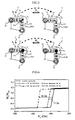
- a single sensor arranged on a support 1 is represented, which includes a ferromagnetic planar structure 3.
- a nanostructure 3 is typically covered by a plurality of layers (not shown) provided for a biosensor, comprising an insulating protective layer, a polymeric layer for attaching the above mentioned binding molecules, and the layer of binding molecules.
- the nanostructure 3 comprises at least one detection area 31 shaped as a strip bent to form a corner. More particularly, the detection area 31 corresponds to a vertex of such corner.
- the nanostructure 3 comprises also a couple of terminal discs 32, obtained at the opposite ends of the detection area 31.
- the nanostructure 3 is for example made of Permalloy.
- reference will be made to a nanostructure made of such a material, having a thickness of 40 nm and a width of the strip in the detection area of 50 nm, and total external dimensions of 0,3 ⁇ m x 0,3 ⁇ m. Such dimensions, however, can be further reduced without detriment for the device functionality.
- a plurality of non-magnetic contacts Iin, GND, V1 and V2 is arranged which can be obtained, for example, through electron beam lithography on the surface of the nanostructure 3.
- the contacts Iin, GND, V1 and V2 are adapted to be linked to measuring means (not illustrated) suitable for measuring the magnetoresistive response of the nanostructure 3 at the ends of the detection area 31.
- two supply contacts lin and GND are present, adapted to be linked to a current supply circuit, to inject an electric current through the detection area 31, and two reading contacts V1 and V2, adapted to be linked to a measuring circuit, for measuring the potential difference between the ends of the detection area 31.
- the above mentioned contacts are, for example, made of Au.
- a first configuration is illustrated, and it comprises a magnetic transversal head-to-head domain wall TW positioned at the corner of the detection area 31 and vortex structures VS, formed inside the terminal discs 32.
- the application of a second magnetic field along the direction x or y displaces the domain wall TW towards one of the terminal discs 32, where it is annihilated in the vortex spin structure, resulting in the second configuration illustrated in figure 2b .
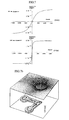
- Figure 3 shows an example of the method for initializing the device, according to which the transversal "head-to-head" domain wall TW is positioned in the angle of the detection angle 31, by applying a magnetic field H 0 (with and intensity, for example, of 1000 Oe) along the angle bisector and subsequently removing such a field.
- H 0 with and intensity, for example, of 1000 Oe
- the two vortex spin structures VS are implemented. Once it has been created, the domain wall TW is stable, and it can be displaced until it is annihilated in one of the vortex spin structures, by applying a magnetic field along the direction x or y.
- Figure 4 shows the removal of a domain wall TW from the corner, by applying a horizontal magnetic field (direction x) H.
- the domain wall TW can be relocated on the angle, by applying a horizontal magnetic field on the opposite direction, or by applying again a field H 0 along the bisector of the angle, as illustrated in figure 4 .
- magnetoresistive measurements are employed, i.e. the measurement of the potential differences V A and V B between the reading contacts V2 and V1, respectively, in the two spin configurations illustrated in figure 4 (corresponding to those in figures 2a and 2b , respectively).
- the magnetoresistance in the nanostructures according to the invention is controlled by the so-called anisotropic magneticresistance effect (AMR), and a maximum resistance is observed (and therefore a maximum potential difference between the reading contacts) when the magnetization is parallel or anti-parallel to the injected flow of current. This corresponds to a condition where there is no domain wall between the two reading contacts V2 and V1, and the magnetization continuously rotate following the corner shape in the detection area 31, resulting in the potential differential V B in figure 4 .
- AMR anisotropic magneticresistance effect
- the high predictability in switching between the two spin configurations and the sharpness of the transition between such configurations allow the nanostructure to be used for detecting the magnetic nanoparticles, as follows.
- a distance corresponds to a predictable thickness for a biosensor, taking into account the layers which cover the nanostructure 30, which is the insulating protective layer, the intermediate polymeric layer and the binding molecule layer (for example, in case of probe molecules formed by DNA strands, the length of such filaments is taken into account).
- Figure 6 shows the effect of the particle diameter on the field, which causes the structure TW to move: using a nanoparticle with a diameter of 100 nm positioned at a vertical distance of 60 nm from the surface of the nanostructure, such a field increases by 35 Oe (broken and dotted line in figure 6 ).
- a domain wall TW was positioned in the selected corner with an external magnetic field, applied along one of the sides of the ring, i.e. following the same procedure described in relation to the corner-shaped nanostructure 3 described herein.
- the inventors have detected a variation (increase) in the potential difference by 1,45 ⁇ V, after removal of the TW from the angle with a noise (with and without the domain wall TW) of 60 nV, corresponding to a signal-to-noise ratio of 24 (which increases to about 60, increasing the time constant of the lock-in amplifier, i.e. the integration range, up to 100 ms).
- This value can be used as a good evaluation of the typical signal-to-noise ratio, which characterizes the detection process of the nanoparticles by the device described herein.
- the device can be operated as follows: first it is initialized, by positioning a domain wall TW in the angle, as shown in figure 3 (the possible presence of the nanoparticle does not affect such a step); a horizontal field H k is then applied, so that H 1x ⁇ H k ⁇ H 2x ; if the potential difference between the two reading contacts V2 and V1 does not change, a magnetized nanoparticle N is sitting on top of the corner; on the contrary, if the potential difference changes (i.e. increases) no nanoparticles are localized on the sensor active area.
- the active area of the device is only the angle portion occupied by the domain wall TW, which is in the same length order as the detection area 31 of the strip, i.e. 50 nm x 50 nm in the concerned example, and it coincides with the portion of the nanostructure 3 included between the reading contacts V2 and V1. Therefore, for detecting a single nanoparticle, the detection area 31 can be adapted to the dimensions of the nanoparticle to be detected, by designing, as a consequence, the width of the bent strip without having to reduce the whole nanostructure 3.
- Figure 7b shows the vector diagram of the force acting on a plane spaced 200 nm from the surface of the sensor on a superparamagnetic nanoparticle with a diameter of 50 nm, characterized by a magnetic moment as a function of the external field, m(H), as shown in the top graph in figure 7a, which is the estimated value for the commercial nanoparticle MACS TM , herein taken into account.
- the bottom graph in figure 7a shows also m(H) for a nanoparticle MACS TM with a diameter of 100 nm.
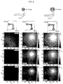
- the level curve diagrams in the central column in figure 8 show that the module of the force acting on the nanoparticle with a 50 nm diameter at a distance of 200 nm from the nanostructure 3 is in the range from 0,5 to 1 pN on an area with a diameter of about 300 nm, guaranteeing effective trapping and focusing actions on a nanoparticle (see the explanation below).
- the module of the force increases by a factor of about 10 if the distance between the nanoparticle and the surface of the nanostructure is reduced to 60 nm.
- the intensity contour plots in the left column in figure 8 show that when the domain wall TW is removed from the corner and annihilated in one of the vortex spin structures VS, the force acting on the nanoparticle at the angle is negligible.
- no external action is required (such as the positioning of the nanoparticle in the correct position, by using an external field inducing also a momentum in the nanoparticle), in order to position and magnetize the particle for an optimal detection.
- the force acting on a nanoparticle can be increased or decreased, by increasing or decreasing the nanostructure thickness, respectively.
- Such an aspect is critical in setting the magnetic focusing and to prevent the particles from grouping, which can result in case of fields with a too high gradient.
- the domain wall TW may be annihilated in the terminal discs, by simply applying an external field, thereby obtaining a condition, wherein the magnetic forces are negligible, as discussed above, with reference to the diagrams in the left column in figure 8 .
- the concept according to the invention allows to activate and deactivate the magnetic focusing, through external fields, without additional current lines, which would increase the device complexity.
- the biosensor array could then operate as follows:
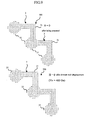
- Figure 9 shows micromagnetic simulations, which illustrate how the corner structure can be repeated in chains, without altering the operation of each unit.
- a chain 300 is made by causing each individual nanostructure 3 to share a proper terminal discs 32 with another nanostructure 3 adjacent thereto.
- Such a configuration is particularly suitable to make an array, arranging a plurality of chains 300 of side-by-side nanostructures.
- the potential difference can be read in a plurality of detection areas 31, linked by reading contacts, such to form a set of resistances in parallel ( figure 10a ) or in series ( figure 10b ).
- FIG 10a part of an array is illustrated, wherein among the side-by-side chains 300, pairs of reading contact strips 310, 320 extend (corresponding to the reading contacts V1 and V2, previously described), wherein each detection area 31 of each nanostructure chain 300 is connected in parallel with a detection area 31 of the other nanostructure chains 300 corresponding thereto for the position, through a respective pair of reading contact strips 310, 320.
- the chains 300 are supplied in parallel through supply contacts Iin and GND.
- FIG 10b part of an array is illustrated, wherein a pair of reading contact strips 410, 420 (corresponding to the reading contacts V1 and V2, previously described), is connected to the opposite ends of each chain 300 on all the chains 300.
- each pair of reading contact strips 310, 320 (in the configuration in figure 10a ) or each current injection contact li in must be sequentially enabled by a multiplexer.
- the impedance of the reading strips 410 and 420 shall be significantly higher than that of the chains.
- the above computed signal-to-noise ratio is such that it can be predicted to have up to 5 detection areas 31, connected in parallel or in series between two reading contacts.
- the sensor active area matching with the detection area 31
- the functionalized area i.e. the area occupied by the binding molecules arranged above the sensors
- the selective functionalization of the individual detection area 31, however, is extremely difficult and not suitable for a large-scale production of the devices; it is, indeed, more reasonable, to assume a functionalized area in the order of 200 ⁇ m 2 , wherein several units of the array can be grouped, such as those represented in figs. 10 and 10b .
- this does not result in a significant loss of biological sensibility, as the auto-focusing tends to concentrate the magnetic nanoparticles on the detection areas 31.
- the functionalized area corresponds to the actual active area of sensors.
- the situation could be even more favourable and the capture area could entirely cover the functionalized area.
- the force acting on the nanoparticle is likely to be sufficiently high to guarantee that the latter would be drawn towards a detection area 31, where the presence thereof can be detected, for any initial position on the functionalized area, but this result needs to be experimentally confirmed.
- the intensity of the magnetic force and the capture area extension can be adjusted in many different ways: (i) changing the thickness and/or the width of the nanostructure 3 strip, or (ii) modifying the angle between the two segments, which define the corner. Reducing the thickness results, for example, in an increase of the variation in the transition field, caused by the vicinity of the magnetic nanoparticle (magnetic signal), even though such an advantage is accompanied by a decrease in the focusing magnetic forces.
- the dynamic range of the arrays, employing the units in figures 10a and 10b can be easily assessed.
- the maximum concentration of detectable nanoparticles is in the order of 5 ⁇ 10 8 nanoparticles/cm 2 , corresponding to a nanoparticle in each detection area 31.
- 70 array units are used, arranged in an area of about 200 ⁇ m, functionalized with the same binding molecule, an array is obtained, which is able to detect only one molecule thereon, i.e. a concentration in the order of 5 ⁇ 10 5 nanoparticles/cm 2 .
Landscapes
- Health & Medical Sciences (AREA)
- Engineering & Computer Science (AREA)
- Immunology (AREA)
- Life Sciences & Earth Sciences (AREA)
- Chemical & Material Sciences (AREA)
- Physics & Mathematics (AREA)
- Urology & Nephrology (AREA)
- General Physics & Mathematics (AREA)
- Biomedical Technology (AREA)
- Hematology (AREA)
- Molecular Biology (AREA)
- Biochemistry (AREA)
- Cell Biology (AREA)
- Food Science & Technology (AREA)
- Medicinal Chemistry (AREA)
- Nanotechnology (AREA)
- Analytical Chemistry (AREA)
- Microbiology (AREA)
- General Health & Medical Sciences (AREA)
- Biotechnology (AREA)
- Pathology (AREA)
- Condensed Matter Physics & Semiconductors (AREA)
- Investigating Or Analyzing Materials By The Use Of Magnetic Means (AREA)
- Transmission And Conversion Of Sensor Element Output (AREA)
Claims (12)
- Sensor zur Detektion des Vorhandenseins magnetischer Nanopartikel, wobei der Sensor Folgendes aufweist:eine Stütze (1), auf welcher der Sensor angeordnet ist;eine Mehrzahl von nicht magnetischen Kontakten (Iin, GND, V1. V2), die auf der Stütze angeordnet und elektrisch leitend mit dem Sensor verbunden sind;Mittel zum Messen des Magnetwiderstands am mit der Mehrzahl von nicht magnetischen Kontakten verbundenen Sensor,dadurch gekennzeichnet, dass:- der Sensor eine ebene ferromagnetische Struktur (3) enthält, die einen Detektionsbereich (31) in der Form eines Bandes aufweist, das gebogen ist, um eine Ecke zu bilden,- der Sensor strukturiert ist, ein Magnetfeld anzulegen, sodass der Detektionsbereich selektiv als Reaktion auf das angelegte Magnetfeld Folgendes annimmt:eine erste Spin-Konfiguration, die eine quer stehende "Kopf-an-Kopf"-Blochwand (TW) aufweist, undeine zweite Spin-Konfiguration, wobei keine derartige Blochwand (TW) vorhanden ist, und wobei der Übergang von der ersten Konfiguration zur zweiten Konfiguration für das angelegte Magnetfeld bereitgestellt wird, mit einer zu einer der abgewinkelten Seiten des Detektionsbereichs parallelen Komponente mit einer höheren Intensität als eine vorhersehbare Übergangsschwelle (H1x), wobei die mittels Magnetwiderstand detektierbare Übergangsschwelle durch die Nähe eines magnetischen Nanopartikels (N) zum Detektionsbereich beeinflusst wird,- die Mittel zum Messen strukturiert sind, um eine Messung der Übergangsschwelle bereitzustellen, anhand von Messungen des Magnetwiderstands des Detektionsbereichs in der ersten und der zweiten Spin-Konfiguration, die bei Anlegen des Magnetfelds angenommen werden.
- Sensor nach Anspruch 1, wobei der Sensor strukturiert ist, sodass der Übergang zwischen der ersten und der zweiten Konfiguration durch einen anisotropischen Magnetwiderstandseffekt geschieht.
- Sensor nach Anspruch 1, wobei die Nanostruktur (3) aus dem Detektions bereich (31) besteht, an dessen entgegengesetzten Enden jeweilige Endscheiben (32) positionieri sind.
- Sensor nach Anspruch 3, wobei die Kontakte ein Paar an entgegengesetzten Enden des Detektionsbereichs (31) angeordnete Injektionskontakte (Iin, GND) umfassen, die ausgelegt sind, die Injektion eines elektrischen Stroms durch den Detektionsbereich (31) zu ermöglichen, und ein Paar an entgegengesetzten Enden des Detektionsbereichs (31) angeordnete Lesekontakte (V1, V2), die ausgelegt sind, eine Messung des Potenzialunterschieds (VA, VB) zwischen den Enden des Detektionsbereichs (31) zu ermöglichen.
- Sensor nach einem der vorhergehenden Ansprüche, wobei die "Kopf-Mi-Kopf"-Blochwand (TW) in der ersten Spin-Konfiguration dazu dient, ein magnetisches Nanopartikel zu erfassen und es zum Detektionsbereich (31) zu treiben.
- Sensor nach einem der vorhergehenden Ansprüche, wobei der Sensor angeordnet ist, Einzelmolekül-Detektion durchzuführen und/oder in Systemen für die Synthese auf Einzelmolekülebene und/oder Analyse auf Einzelmolekülebene eingesetzt zu werden.
- Sensoranordnung zum Detektieren von Zielmolekülen, an die magnetische Nanopartikel (N) als Marker gebunden sind, wobei die Sensoranordnung eine Stütze (1) aufweist, an der Folgendes vorgesehen ist:eine Mehrzahl von Detektionsstellen (DS), zu denen jeweilige Bindungsmoleküle gehören, die ausgelegt sind, selektiv an die Zielmoleküle zu binden, und jeweilige Sensoren, von denen jeder ausgelegt ist, das Vorhandensein eines magnetischen Nanopartikels (N) an der jeweiligen Detektionsstelle (DS) zu detektieren,dadurch gekennzeichnet, dass jeder Sensor nach einem der vorhergehenden Ansprüche realisiert ist.
- Anordnung nach Anspruch 7, wobei die Sensoren angeordnet sind, eine Mehrzahl von Seite an Seite liegenden Sensorketten (300) zu bilden, wobei jede Sensorkette aus einer Mehrzahl von einstückigen Nanostrukturen (3) besteht und jede einstückige Nanostruktur (3) aus dem Detektionsbereich (31) in der Form eines Bandes besteht, das gebogen ist, um eine Ecke zu bilden, und an dessen Enden jeweilige Endscheiben (32) positioniert sind, wobei die einstückigen Nanostrukturen derart verbunden sind, dass sich jede einstückige Nanostruktur eine Endscheibe (32) mit der folgenden teilt.
- Anordnung nach Anspruch 8, wobei die Kontakte eine Mehrzahl von Injektionskontakten (Iin, GND; Hin, GND) umfassen, die ausgelegt sind, die Injektion eines elektrischen Stroms durch den Detektionsbereich (31) jeder einstückigen Nanostruktur zu ermöglichen, und eine Mehrzahl von Lesekontakten (310, 320; 410, 420), die ausgelegt sind, eine Messung des Potenzialunterschieds zwischen den Enden des Detektionsbereichs (31) jeder Nanostruktureinheit zu ermöglichen.
- Anordnung nach Anspruch 9, wobei die Lesekontakte (310, 320) derart angeordnet sind, dass die Detektionsbereiche (31) der entsprechenden einstückigen Nanostrukturen an der Position der unterschiedlichen Sensorketten (300) parallel verbunden sind, wobei die Sensorketten parallel mit einem Paar Injektionskontakten (Iin, GND) verbunden sind, um die zeitgleiche Injektion der jeweiligen elektrischen Ströme durch die Sensorketten (300) zu ermöglichen.
- Anordnung nach Anspruch 9, wobei die Lesekontakte (410, 420) zwei sind und zeitgleich mit den unterschiedlichen Sensorketten (300) verbunden sind, und derart angeordnet sind, dass die Detektionsbereiche (31) jeder Sensorkette seriell verbunden sind, wobei jede Sensorkette mit einem jeweiligen Kontakt (Iiin) der Injektionskontakte verbunden ist, um die unabhängige Injektion eines jeweiligen elektrischen Stroms durch jede Sensorkette zu ermöglichten.
- Verfahren zum Detektieren von Zielmolekülen, mit denen magnetische Nanopartikel (N) als Marker verknüpft sind, wobei das Verfahren die folgenden Schritte umfasst:Bereitstellen einer Sensoranordnung nach einem der Ansprüche 7 bis 11;Anlegen eines ersten Magnetfelds, um die erste Spin-Konfiguration in jeder Nanostruktur (3) zu erzielen, und darauf folgend Entfernen des ersten Magnetfelds;Abgeben einer biologischen Probe, welche die Zielmoleküle enthält, auf die Detektionsstellen (DS);Anlegen eines zweiten Magnetfelds, um von der ersten Spin-Konfiguration zur zweiten Spin-Konfiguration in jeder Nanostruktur (3) zu wechseln, und darauf folgend Entfernen des zweiten Magnetfelds;Entfernen der Zielmoleküle, die nicht chemisch mit den Bindungsmolekülen verknüpft sind, von den Detektionsstellen (DS);Anlegen eines dritten Magnetfelds, um erneut die erste Spin-Konfiguration in jeder Nanostruktur (3) zu erzielen, und darauf folgend Entfernen des dritten Magnetfelds; undDurchführen von Messungen des kritischen Übergangsfelds von der ersten Spin-Konfiguration zur zweiten Spin-Konfiguration durch Messungen des Magnetwiderstands an den Sensoren durch die Mehrzahl von Kontakten.
Applications Claiming Priority (2)
| Application Number | Priority Date | Filing Date | Title |
|---|---|---|---|
| IT000314A ITTO20080314A1 (it) | 2008-04-23 | 2008-04-23 | Biosensori spintronici con area attiva localizzata su una parete di dominio magnetico. |
| PCT/EP2009/054808 WO2009130241A1 (en) | 2008-04-23 | 2009-04-22 | Spintronic magnetic nanoparticle sensors with an active area located on a magnetic domain wall |
Publications (2)
| Publication Number | Publication Date |
|---|---|
| EP2274633A1 EP2274633A1 (de) | 2011-01-19 |
| EP2274633B1 true EP2274633B1 (de) | 2012-08-08 |
Family
ID=40297326
Family Applications (1)
| Application Number | Title | Priority Date | Filing Date |
|---|---|---|---|
| EP09734585A Not-in-force EP2274633B1 (de) | 2008-04-23 | 2009-04-22 | Magnetische spintronic-nanopartikelsensoren mit einem auf einer magnetischen domänenwand angeordneten aktiven bereich |
Country Status (5)
| Country | Link |
|---|---|
| US (1) | US8779763B2 (de) |
| EP (1) | EP2274633B1 (de) |
| ES (1) | ES2390403T3 (de) |
| IT (1) | ITTO20080314A1 (de) |
| WO (1) | WO2009130241A1 (de) |
Families Citing this family (11)
| Publication number | Priority date | Publication date | Assignee | Title |
|---|---|---|---|---|
| US11237171B2 (en) | 2006-02-21 | 2022-02-01 | Trustees Of Tufts College | Methods and arrays for target analyte detection and determination of target analyte concentration in solution |
| US8492098B2 (en) | 2006-02-21 | 2013-07-23 | The Trustees Of Tufts College | Methods and arrays for target analyte detection and determination of reaction components that affect a reaction |
| WO2009029073A1 (en) | 2007-08-30 | 2009-03-05 | The Trustees Of Tufts College | Methods for determining the concentration of an analyte in solution. |
| IT1392999B1 (it) | 2009-02-12 | 2012-04-02 | Ct De Investigacion Cooperativa En Nanociencias Cic Nanogune Asoc | Manipolazione di particelle magnetiche in circuiti per la propagazione di pareti di dominio magnetiche. |
| US8236574B2 (en) | 2010-03-01 | 2012-08-07 | Quanterix Corporation | Ultra-sensitive detection of molecules or particles using beads or other capture objects |
| CN103026232B (zh) * | 2010-03-01 | 2015-02-04 | 匡特里克斯公司 | 扩大用于检测分子或颗粒的测定法中的动态范围的方法和系统 |
| US9952237B2 (en) | 2011-01-28 | 2018-04-24 | Quanterix Corporation | Systems, devices, and methods for ultra-sensitive detection of molecules or particles |
| US8933521B2 (en) * | 2011-03-30 | 2015-01-13 | Intel Corporation | Three-dimensional magnetic circuits including magnetic connectors |
| US20140302532A1 (en) | 2011-04-12 | 2014-10-09 | Quanterix Corporation | Methods of determining a treatment protocol for and/or a prognosis of a patient's recovery from a brain injury |
| US9932626B2 (en) | 2013-01-15 | 2018-04-03 | Quanterix Corporation | Detection of DNA or RNA using single molecule arrays and other techniques |
| WO2015157184A1 (en) | 2014-04-07 | 2015-10-15 | The Regents Of The University Of California | Highly tunable magnetic liquid crystals |
Family Cites Families (6)
| Publication number | Priority date | Publication date | Assignee | Title |
|---|---|---|---|---|
| DE19619806A1 (de) * | 1996-05-15 | 1997-11-20 | Siemens Ag | Magnetfeldempfindliche Sensoreinrichtung mit mehreren GMR-Sensorelementen |
| WO2003039753A1 (en) * | 2001-11-05 | 2003-05-15 | President And Fellows Of Harvard College | System and method for capturing and positioning particles |
| US7034374B2 (en) * | 2003-08-22 | 2006-04-25 | Micron Technology, Inc. | MRAM layer having domain wall traps |
| US7242604B2 (en) | 2005-01-13 | 2007-07-10 | International Business Machines Corporation | Switchable element |
| WO2007015055A1 (en) | 2005-08-03 | 2007-02-08 | Ingenia Technology Limited | Memory access |
| WO2009143444A1 (en) * | 2008-05-22 | 2009-11-26 | The Ohio State University | Mobile mangnetic traps and platforms for micro/nano particle manipulation |
-
2008
- 2008-04-23 IT IT000314A patent/ITTO20080314A1/it unknown
-
2009
- 2009-04-22 ES ES09734585T patent/ES2390403T3/es active Active
- 2009-04-22 WO PCT/EP2009/054808 patent/WO2009130241A1/en active Application Filing
- 2009-04-22 US US12/989,576 patent/US8779763B2/en not_active Expired - Fee Related
- 2009-04-22 EP EP09734585A patent/EP2274633B1/de not_active Not-in-force
Also Published As
| Publication number | Publication date |
|---|---|
| EP2274633A1 (de) | 2011-01-19 |
| ES2390403T3 (es) | 2012-11-12 |
| US20110037463A1 (en) | 2011-02-17 |
| US8779763B2 (en) | 2014-07-15 |
| ITTO20080314A1 (it) | 2009-10-24 |
| WO2009130241A1 (en) | 2009-10-29 |
Similar Documents
| Publication | Publication Date | Title |
|---|---|---|
| EP2274633B1 (de) | Magnetische spintronic-nanopartikelsensoren mit einem auf einer magnetischen domänenwand angeordneten aktiven bereich | |
| Nabaei et al. | Magnetic biosensors: Modelling and simulation | |
| US6468809B1 (en) | High efficiency magnetic sensor for magnetic particles | |
| US7906345B2 (en) | Magnetic nanoparticles, magnetic detector arrays, and methods for their use in detecting biological molecules | |
| KR20040068968A (ko) | 마이크로-어레이상의 자기 나노입자들의 면적 밀도를측정하는 센서 및 방법 | |
| KR20060054351A (ko) | 개선된 신호대 잡음비를 가진 온칩 자기 입자 센서 | |
| US20100176807A1 (en) | Magnetic sensor device | |
| JP2008522149A (ja) | 磁気センサの伝達関数を校正するための方法 | |
| US20090309588A1 (en) | System and methods for actuation on magnetoresistive sensors | |
| US7651871B2 (en) | Device for forming magnetic well for nanoparticles | |
| US20090280571A1 (en) | Microelectronic device with magnetic manipulator | |
| Brückl et al. | Magnetic particles as markers and carriers of biomolecules | |
| EP1967855A1 (de) | Magnetsensorvorrichtung | |
| Kasatkin et al. | Biosensors based on the thin-film magnetoresistive sensors | |
| Porter et al. | Method and apparatus for magnetoresistive monitoring of analytes in flow streams |
Legal Events
| Date | Code | Title | Description |
|---|---|---|---|
| PUAI | Public reference made under article 153(3) epc to a published international application that has entered the european phase |
Free format text: ORIGINAL CODE: 0009012 |
|
| 17P | Request for examination filed |
Effective date: 20101028 |
|
| AK | Designated contracting states |
Kind code of ref document: A1 Designated state(s): AT BE BG CH CY CZ DE DK EE ES FI FR GB GR HR HU IE IS IT LI LT LU LV MC MK MT NL NO PL PT RO SE SI SK TR |
|
| AX | Request for extension of the european patent |
Extension state: AL BA RS |
|
| DAX | Request for extension of the european patent (deleted) | ||
| 17Q | First examination report despatched |
Effective date: 20110718 |
|
| GRAP | Despatch of communication of intention to grant a patent |
Free format text: ORIGINAL CODE: EPIDOSNIGR1 |
|
| GRAS | Grant fee paid |
Free format text: ORIGINAL CODE: EPIDOSNIGR3 |
|
| GRAA | (expected) grant |
Free format text: ORIGINAL CODE: 0009210 |
|
| AK | Designated contracting states |
Kind code of ref document: B1 Designated state(s): AT BE BG CH CY CZ DE DK EE ES FI FR GB GR HR HU IE IS IT LI LT LU LV MC MK MT NL NO PL PT RO SE SI SK TR |
|
| REG | Reference to a national code |
Ref country code: GB Ref legal event code: FG4D |
|
| REG | Reference to a national code |
Ref country code: AT Ref legal event code: REF Ref document number: 570046 Country of ref document: AT Kind code of ref document: T Effective date: 20120815 Ref country code: CH Ref legal event code: EP |
|
| REG | Reference to a national code |
Ref country code: DE Ref legal event code: R082 Ref document number: 602009008845 Country of ref document: DE Representative=s name: CABINET CHAILLOT, FR |
|
| REG | Reference to a national code |
Ref country code: IE Ref legal event code: FG4D |
|
| REG | Reference to a national code |
Ref country code: DE Ref legal event code: R096 Ref document number: 602009008845 Country of ref document: DE Effective date: 20121004 |
|
| REG | Reference to a national code |
Ref country code: ES Ref legal event code: FG2A Ref document number: 2390403 Country of ref document: ES Kind code of ref document: T3 Effective date: 20121112 |
|
| REG | Reference to a national code |
Ref country code: NL Ref legal event code: VDEP Effective date: 20120808 |
|
| REG | Reference to a national code |
Ref country code: AT Ref legal event code: MK05 Ref document number: 570046 Country of ref document: AT Kind code of ref document: T Effective date: 20120808 |
|
| REG | Reference to a national code |
Ref country code: LT Ref legal event code: MG4D Effective date: 20120808 |
|
| PG25 | Lapsed in a contracting state [announced via postgrant information from national office to epo] |
Ref country code: CY Free format text: LAPSE BECAUSE OF FAILURE TO SUBMIT A TRANSLATION OF THE DESCRIPTION OR TO PAY THE FEE WITHIN THE PRESCRIBED TIME-LIMIT Effective date: 20120808 Ref country code: FI Free format text: LAPSE BECAUSE OF FAILURE TO SUBMIT A TRANSLATION OF THE DESCRIPTION OR TO PAY THE FEE WITHIN THE PRESCRIBED TIME-LIMIT Effective date: 20120808 Ref country code: HR Free format text: LAPSE BECAUSE OF FAILURE TO SUBMIT A TRANSLATION OF THE DESCRIPTION OR TO PAY THE FEE WITHIN THE PRESCRIBED TIME-LIMIT Effective date: 20120808 Ref country code: IS Free format text: LAPSE BECAUSE OF FAILURE TO SUBMIT A TRANSLATION OF THE DESCRIPTION OR TO PAY THE FEE WITHIN THE PRESCRIBED TIME-LIMIT Effective date: 20121208 Ref country code: AT Free format text: LAPSE BECAUSE OF FAILURE TO SUBMIT A TRANSLATION OF THE DESCRIPTION OR TO PAY THE FEE WITHIN THE PRESCRIBED TIME-LIMIT Effective date: 20120808 Ref country code: NO Free format text: LAPSE BECAUSE OF FAILURE TO SUBMIT A TRANSLATION OF THE DESCRIPTION OR TO PAY THE FEE WITHIN THE PRESCRIBED TIME-LIMIT Effective date: 20121108 Ref country code: LT Free format text: LAPSE BECAUSE OF FAILURE TO SUBMIT A TRANSLATION OF THE DESCRIPTION OR TO PAY THE FEE WITHIN THE PRESCRIBED TIME-LIMIT Effective date: 20120808 |
|
| PG25 | Lapsed in a contracting state [announced via postgrant information from national office to epo] |
Ref country code: BE Free format text: LAPSE BECAUSE OF FAILURE TO SUBMIT A TRANSLATION OF THE DESCRIPTION OR TO PAY THE FEE WITHIN THE PRESCRIBED TIME-LIMIT Effective date: 20120808 Ref country code: PT Free format text: LAPSE BECAUSE OF FAILURE TO SUBMIT A TRANSLATION OF THE DESCRIPTION OR TO PAY THE FEE WITHIN THE PRESCRIBED TIME-LIMIT Effective date: 20121210 Ref country code: SI Free format text: LAPSE BECAUSE OF FAILURE TO SUBMIT A TRANSLATION OF THE DESCRIPTION OR TO PAY THE FEE WITHIN THE PRESCRIBED TIME-LIMIT Effective date: 20120808 Ref country code: GR Free format text: LAPSE BECAUSE OF FAILURE TO SUBMIT A TRANSLATION OF THE DESCRIPTION OR TO PAY THE FEE WITHIN THE PRESCRIBED TIME-LIMIT Effective date: 20121109 Ref country code: LV Free format text: LAPSE BECAUSE OF FAILURE TO SUBMIT A TRANSLATION OF THE DESCRIPTION OR TO PAY THE FEE WITHIN THE PRESCRIBED TIME-LIMIT Effective date: 20120808 Ref country code: PL Free format text: LAPSE BECAUSE OF FAILURE TO SUBMIT A TRANSLATION OF THE DESCRIPTION OR TO PAY THE FEE WITHIN THE PRESCRIBED TIME-LIMIT Effective date: 20120808 Ref country code: SE Free format text: LAPSE BECAUSE OF FAILURE TO SUBMIT A TRANSLATION OF THE DESCRIPTION OR TO PAY THE FEE WITHIN THE PRESCRIBED TIME-LIMIT Effective date: 20120808 |
|
| PG25 | Lapsed in a contracting state [announced via postgrant information from national office to epo] |
Ref country code: NL Free format text: LAPSE BECAUSE OF FAILURE TO SUBMIT A TRANSLATION OF THE DESCRIPTION OR TO PAY THE FEE WITHIN THE PRESCRIBED TIME-LIMIT Effective date: 20120808 |
|
| PG25 | Lapsed in a contracting state [announced via postgrant information from national office to epo] |
Ref country code: RO Free format text: LAPSE BECAUSE OF FAILURE TO SUBMIT A TRANSLATION OF THE DESCRIPTION OR TO PAY THE FEE WITHIN THE PRESCRIBED TIME-LIMIT Effective date: 20120808 Ref country code: DK Free format text: LAPSE BECAUSE OF FAILURE TO SUBMIT A TRANSLATION OF THE DESCRIPTION OR TO PAY THE FEE WITHIN THE PRESCRIBED TIME-LIMIT Effective date: 20120808 Ref country code: CZ Free format text: LAPSE BECAUSE OF FAILURE TO SUBMIT A TRANSLATION OF THE DESCRIPTION OR TO PAY THE FEE WITHIN THE PRESCRIBED TIME-LIMIT Effective date: 20120808 Ref country code: EE Free format text: LAPSE BECAUSE OF FAILURE TO SUBMIT A TRANSLATION OF THE DESCRIPTION OR TO PAY THE FEE WITHIN THE PRESCRIBED TIME-LIMIT Effective date: 20120808 |
|
| PG25 | Lapsed in a contracting state [announced via postgrant information from national office to epo] |
Ref country code: SK Free format text: LAPSE BECAUSE OF FAILURE TO SUBMIT A TRANSLATION OF THE DESCRIPTION OR TO PAY THE FEE WITHIN THE PRESCRIBED TIME-LIMIT Effective date: 20120808 |
|
| PLBE | No opposition filed within time limit |
Free format text: ORIGINAL CODE: 0009261 |
|
| STAA | Information on the status of an ep patent application or granted ep patent |
Free format text: STATUS: NO OPPOSITION FILED WITHIN TIME LIMIT |
|
| 26N | No opposition filed |
Effective date: 20130510 |
|
| PG25 | Lapsed in a contracting state [announced via postgrant information from national office to epo] |
Ref country code: BG Free format text: LAPSE BECAUSE OF FAILURE TO SUBMIT A TRANSLATION OF THE DESCRIPTION OR TO PAY THE FEE WITHIN THE PRESCRIBED TIME-LIMIT Effective date: 20121108 |
|
| REG | Reference to a national code |
Ref country code: DE Ref legal event code: R097 Ref document number: 602009008845 Country of ref document: DE Effective date: 20130510 |
|
| PG25 | Lapsed in a contracting state [announced via postgrant information from national office to epo] |
Ref country code: MC Free format text: LAPSE BECAUSE OF FAILURE TO SUBMIT A TRANSLATION OF THE DESCRIPTION OR TO PAY THE FEE WITHIN THE PRESCRIBED TIME-LIMIT Effective date: 20120808 |
|
| REG | Reference to a national code |
Ref country code: CH Ref legal event code: PL |
|
| REG | Reference to a national code |
Ref country code: IE Ref legal event code: MM4A |
|
| PG25 | Lapsed in a contracting state [announced via postgrant information from national office to epo] |
Ref country code: LI Free format text: LAPSE BECAUSE OF NON-PAYMENT OF DUE FEES Effective date: 20130430 Ref country code: CH Free format text: LAPSE BECAUSE OF NON-PAYMENT OF DUE FEES Effective date: 20130430 |
|
| PG25 | Lapsed in a contracting state [announced via postgrant information from national office to epo] |
Ref country code: IE Free format text: LAPSE BECAUSE OF NON-PAYMENT OF DUE FEES Effective date: 20130422 |
|
| PG25 | Lapsed in a contracting state [announced via postgrant information from national office to epo] |
Ref country code: MT Free format text: LAPSE BECAUSE OF FAILURE TO SUBMIT A TRANSLATION OF THE DESCRIPTION OR TO PAY THE FEE WITHIN THE PRESCRIBED TIME-LIMIT Effective date: 20120808 |
|
| PG25 | Lapsed in a contracting state [announced via postgrant information from national office to epo] |
Ref country code: TR Free format text: LAPSE BECAUSE OF FAILURE TO SUBMIT A TRANSLATION OF THE DESCRIPTION OR TO PAY THE FEE WITHIN THE PRESCRIBED TIME-LIMIT Effective date: 20120808 |
|
| PG25 | Lapsed in a contracting state [announced via postgrant information from national office to epo] |
Ref country code: MK Free format text: LAPSE BECAUSE OF FAILURE TO SUBMIT A TRANSLATION OF THE DESCRIPTION OR TO PAY THE FEE WITHIN THE PRESCRIBED TIME-LIMIT Effective date: 20120808 Ref country code: LU Free format text: LAPSE BECAUSE OF NON-PAYMENT OF DUE FEES Effective date: 20130422 Ref country code: HU Free format text: LAPSE BECAUSE OF FAILURE TO SUBMIT A TRANSLATION OF THE DESCRIPTION OR TO PAY THE FEE WITHIN THE PRESCRIBED TIME-LIMIT; INVALID AB INITIO Effective date: 20090422 |
|
| REG | Reference to a national code |
Ref country code: FR Ref legal event code: PLFP Year of fee payment: 8 |
|
| REG | Reference to a national code |
Ref country code: FR Ref legal event code: PLFP Year of fee payment: 9 |
|
| PGFP | Annual fee paid to national office [announced via postgrant information from national office to epo] |
Ref country code: ES Payment date: 20170214 Year of fee payment: 9 |
|
| PGFP | Annual fee paid to national office [announced via postgrant information from national office to epo] |
Ref country code: GB Payment date: 20170426 Year of fee payment: 9 Ref country code: FR Payment date: 20170425 Year of fee payment: 9 Ref country code: DE Payment date: 20170426 Year of fee payment: 9 |
|
| PGFP | Annual fee paid to national office [announced via postgrant information from national office to epo] |
Ref country code: IT Payment date: 20170428 Year of fee payment: 9 |
|
| REG | Reference to a national code |
Ref country code: DE Ref legal event code: R119 Ref document number: 602009008845 Country of ref document: DE |
|
| GBPC | Gb: european patent ceased through non-payment of renewal fee |
Effective date: 20180422 |
|
| PG25 | Lapsed in a contracting state [announced via postgrant information from national office to epo] |
Ref country code: DE Free format text: LAPSE BECAUSE OF NON-PAYMENT OF DUE FEES Effective date: 20181101 |
|
| PG25 | Lapsed in a contracting state [announced via postgrant information from national office to epo] |
Ref country code: GB Free format text: LAPSE BECAUSE OF NON-PAYMENT OF DUE FEES Effective date: 20180422 |
|
| PG25 | Lapsed in a contracting state [announced via postgrant information from national office to epo] |
Ref country code: IT Free format text: LAPSE BECAUSE OF NON-PAYMENT OF DUE FEES Effective date: 20180422 Ref country code: FR Free format text: LAPSE BECAUSE OF NON-PAYMENT OF DUE FEES Effective date: 20180430 |
|
| REG | Reference to a national code |
Ref country code: ES Ref legal event code: FD2A Effective date: 20190912 |
|
| PG25 | Lapsed in a contracting state [announced via postgrant information from national office to epo] |
Ref country code: ES Free format text: LAPSE BECAUSE OF NON-PAYMENT OF DUE FEES Effective date: 20180423 |