EP2271077A1 - Method and apparatus for suppressing noise in image sensor devices - Google Patents
Method and apparatus for suppressing noise in image sensor devices Download PDFInfo
- Publication number
- EP2271077A1 EP2271077A1 EP10165083A EP10165083A EP2271077A1 EP 2271077 A1 EP2271077 A1 EP 2271077A1 EP 10165083 A EP10165083 A EP 10165083A EP 10165083 A EP10165083 A EP 10165083A EP 2271077 A1 EP2271077 A1 EP 2271077A1
- Authority
- EP
- European Patent Office
- Prior art keywords
- reset
- converter
- data output
- reading circuit
- correction processing
- Prior art date
- Legal status (The legal status is an assumption and is not a legal conclusion. Google has not performed a legal analysis and makes no representation as to the accuracy of the status listed.)
- Granted
Links
- 238000000034 method Methods 0.000 title claims description 11
- 238000012545 processing Methods 0.000 claims abstract description 174
- 238000012937 correction Methods 0.000 claims abstract description 94
- 230000005855 radiation Effects 0.000 claims abstract description 35
- 239000011159 matrix material Substances 0.000 claims abstract description 10
- 238000012935 Averaging Methods 0.000 claims description 10
- 230000003321 amplification Effects 0.000 description 38
- 238000003199 nucleic acid amplification method Methods 0.000 description 38
- 238000005070 sampling Methods 0.000 description 31
- 238000006243 chemical reaction Methods 0.000 description 20
- 239000003990 capacitor Substances 0.000 description 17
- 238000010586 diagram Methods 0.000 description 16
- 238000003384 imaging method Methods 0.000 description 16
- 239000000872 buffer Substances 0.000 description 15
- 238000001514 detection method Methods 0.000 description 10
- 238000012546 transfer Methods 0.000 description 7
- 238000002594 fluoroscopy Methods 0.000 description 6
- 238000003745 diagnosis Methods 0.000 description 5
- 230000000694 effects Effects 0.000 description 4
- 238000001914 filtration Methods 0.000 description 3
- 238000007689 inspection Methods 0.000 description 3
- 230000004044 response Effects 0.000 description 3
- 239000000758 substrate Substances 0.000 description 3
- 239000010408 film Substances 0.000 description 2
- 238000012360 testing method Methods 0.000 description 2
- 206010073306 Exposure to radiation Diseases 0.000 description 1
- 230000005260 alpha ray Effects 0.000 description 1
- 229910021417 amorphous silicon Inorganic materials 0.000 description 1
- 230000005250 beta ray Effects 0.000 description 1
- 230000005540 biological transmission Effects 0.000 description 1
- 238000002438 flame photometric detection Methods 0.000 description 1
- 230000006870 function Effects 0.000 description 1
- 230000005251 gamma ray Effects 0.000 description 1
- 239000011521 glass Substances 0.000 description 1
- 230000010354 integration Effects 0.000 description 1
- 239000000463 material Substances 0.000 description 1
- 238000012986 modification Methods 0.000 description 1
- 230000004048 modification Effects 0.000 description 1
- 230000003287 optical effect Effects 0.000 description 1
- 239000004065 semiconductor Substances 0.000 description 1
- 238000001228 spectrum Methods 0.000 description 1
- 239000010409 thin film Substances 0.000 description 1
Images




Classifications
-
- H—ELECTRICITY
- H04—ELECTRIC COMMUNICATION TECHNIQUE
- H04N—PICTORIAL COMMUNICATION, e.g. TELEVISION
- H04N25/00—Circuitry of solid-state image sensors [SSIS]; Control thereof
-
- H—ELECTRICITY
- H04—ELECTRIC COMMUNICATION TECHNIQUE
- H04N—PICTORIAL COMMUNICATION, e.g. TELEVISION
- H04N25/00—Circuitry of solid-state image sensors [SSIS]; Control thereof
- H04N25/60—Noise processing, e.g. detecting, correcting, reducing or removing noise
- H04N25/616—Noise processing, e.g. detecting, correcting, reducing or removing noise involving a correlated sampling function, e.g. correlated double sampling [CDS] or triple sampling
-
- H—ELECTRICITY
- H04—ELECTRIC COMMUNICATION TECHNIQUE
- H04N—PICTORIAL COMMUNICATION, e.g. TELEVISION
- H04N25/00—Circuitry of solid-state image sensors [SSIS]; Control thereof
- H04N25/60—Noise processing, e.g. detecting, correcting, reducing or removing noise
- H04N25/618—Noise processing, e.g. detecting, correcting, reducing or removing noise for random or high-frequency noise
-
- H—ELECTRICITY
- H04—ELECTRIC COMMUNICATION TECHNIQUE
- H04N—PICTORIAL COMMUNICATION, e.g. TELEVISION
- H04N25/00—Circuitry of solid-state image sensors [SSIS]; Control thereof
- H04N25/70—SSIS architectures; Circuits associated therewith
- H04N25/76—Addressed sensors, e.g. MOS or CMOS sensors
- H04N25/78—Readout circuits for addressed sensors, e.g. output amplifiers or A/D converters
Definitions
- the present invention relates to image pickup apparatuses, radiation imaging apparatuses, and image pickup systems which are suitable for medical diagnosis or industrial nondestructive inspection, and, more particularly, to an image pickup apparatus, a radiation imaging apparatus, and an image pickup system capable of reading a signal output from a planar detector as digital data using low-noise reading circuitry.
- radiation imaging apparatuses using a planar detector (hereinafter referred to as a Flat Panel Detector (FPD)) made of a semiconductor material are in practical use as image pickup apparatuses used for a medical image diagnosis or a nondestructive inspection using an X-ray.
- Radiation imaging apparatuses using the FPD can perform digital photographing by converting radiation such as an X-ray that has passed through a test object such as a patient into an analog electric signal with the FPD and converting the analog electric signal into a digital image signal.
- FPDs may be used as digital image pickup apparatuses for still image capturing (general image capturing) and moving image capturing (fluoroscopy).
- U.S. Patent No. 6538591 and Japanese Patent Laid-Open No. 2000-188724 disclose signal output circuits (reading circuits) used in image pickup apparatuses as those described above.
- U.S. Patent No. 6538591 discloses a signal transfer apparatus for sequentially reading parallel signals from a plurality of computation amplifiers as a serial signal using a reading switch and converting a serial signal transmitted via an output buffer amplifier into digital data with an analog-to-digital (A/D) conversion circuit (ADC) unit.
- ADC analog-to-digital
- Japanese Patent Laid-Open No. 2000-188724 discloses a circuit obtained by disposing a programmable gain amplifier (PGA) at a stage prior to the output buffer amplifier in the signal transfer apparatus disclosed in U.S. Patent No. 6538591 .
- PGA programmable gain amplifier
- the signal transfer apparatus disclosed in U.S. Patent No. 6538591 and the circuit disclosed in Japanese Patent Laid-Open No. 2000-188724 have an excellent signal-to-noise ratio (S/N) property and a high reading speed, and are suitable for the increase in the number of pixels.
- S/N signal-to-noise ratio
- the present invention provides an image pickup apparatus and an image pickup system capable of reducing an artifact caused by 1/f noise on an acquired image even if small elements are used in the signal output circuits.
- the present invention in its first aspect provides an image pickup apparatus as specified in claims 1 to 7.
- the present invention in its second aspect provides an image pickup system as specified in claim 8.
- the present invention in its third aspect provides a control method as specified in claims 9 to 15.
- an image pickup apparatus and an image pickup system capable of reducing an artifact caused by 1/f noise on an acquired image even if small elements are used.
- Fig. 1 is a schematic block diagram of an image pickup apparatus according to a first embodiment of the present invention.
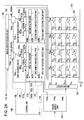
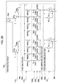
- Figs. 2A and 2B are schematic equivalent circuit diagrams of an image pickup apparatus according to the first embodiment of the present invention.
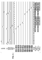
- Fig. 3 is a timing chart describing an image pickup operation performed by an image pickup apparatus according to the first embodiment of the present invention.
- Fig. 4A is a block diagram illustrating a correction processing unit included in an image pickup apparatus according to the first embodiment of the present invention.
- Fig. 4B is a timing chart describing correction processing performed by an image pickup apparatus according to the first embodiment of the present invention.
- Figs. 5A and 5B are exemplary images that illustrate the effect of an embodiment of the present invention.
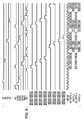
- Fig. 6 is a timing chart describing an image pickup operation performed by an image pickup apparatus according to a second embodiment of the present invention.
- Fig. 7 is a block diagram illustrating a correction processing unit included in an image pickup apparatus according to the second embodiment of the present invention.
- Fig. 8 is a timing chart describing an image pickup operation performed by an image pickup apparatus according to a third embodiment of the present invention.
- Fig. 9 is an equivalent circuit diagram of a reading circuit included in an image pickup apparatus according to a fourth embodiment of the present invention.
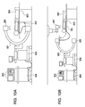
- Figs. 10A and 10B are schematic diagrams describing a radiation imaging system using an image pickup apparatus according to an embodiment of the present invention.
- FIG. 1 is a schematic block diagram of an image pickup apparatus according to the first embodiment of the present invention.
- an image pickup apparatus 100 includes a detection unit 101 in which a plurality of pixels for converting a radiation or light into an analog electric signal are arranged in a matrix, and a driving circuit 102 for driving the detection unit 101 to cause the detection unit 101 to output an analog electric signal.
- the detection unit 101 includes pixels in a matrix of eight rows ⁇ eight columns, and is divided into a first pixel group 101a including four pixel columns and a second pixel group 101b including four pixel columns.
- a pixel signal that is an analog electric signal output from a pixel included in the first pixel group 101a is read by a first reading circuit 103a.
- a pixel signal 113 output from the first reading circuit 103a is converted into digital data 114 by a first A/D converter 104a.
- An analog electric signal output from the second pixel group 101b is read by a second reading circuit 103b and is then converted into digital data by a second A/D converter 104b.
- Pieces of digital data output from the first A/D converter 104a and the second A/D converter 104b are subjected to signal processing (to be described later), digital multiplex processing, offset correction, etc. in a digital data processing unit 105 and are then output as a digital image signal.
- a signal processing section 106 includes a reading circuit unit 103 including the first reading circuit 103a and the second reading circuit 103b, an A/D conversion unit 104 including the first A/D converter 104a and the second A/D converter 104b, and the digital data processing unit 105.
- the image pickup apparatus 100 further includes a power supply unit 107 for supplying a corresponding bias to the signal processing section 106.
- the power supply unit 107 supplies a reference voltage Vref 1 , Vref 2 , or Vref 3 to the reading circuit unit 103, and A/D conversion unit 104.
- the image pickup apparatus 100 further includes a control unit 108 for controlling at least one of the signal processing section 106 and the power supply unit 107.
- the control unit 108 supplies a control signal 118 to the power supply unit 107, supplies control signals 116, 117, and 120 to the reading circuit unit 103, and supplies a driving control signal 119 to the driving circuit 102.
- the driving circuit 102 supplies a driving signal 111 to the detection unit 101.
- Fig. 2A is a schematic equivalent circuit diagram of an image pickup apparatus according to the first embodiment of the present invention.
- the detection unit 101 includes pixels 201 arranged in a matrix. Referring to Fig. 2A , the number of pixels 201 in the matrix is 8 ⁇ 8 pixels, and are arranged in eight rows and eight columns.
- Each of the pixels 201 includes a conversion element S for converting a radiation or light into an electrical charge and a switch element T for outputting an electric signal corresponding to the electrical charge.
- a photoelectric conversion element for example, a PIN photodiode that is mainly made of amorphous silicon and is disposed on an insulating substrate such as a glass substrate, is preferably used.
- an indirect conversion element obtained by providing a wavelength converter for converting a radiation into light of detectable spectrum band on the radiation entering side of the above-described photoelectric conversion element or a direct conversion element for directly converting a radiation into an electrical charge is preferably used.
- the switch element T a transistor having a control terminal and two main terminals is preferably used.
- a thin-film transistor (TFT) is used as the switch element T.
- One electrode of the conversion element S is electrically connected to one of two main terminals of the switch element T, and the other electrode of the conversion element S is electrically connected to a bias power supply 107 via a common line.
- the switch elements T included in a plurality of pixels in the row direction for example, the switch elements T 11 to T 18 , individually have control terminals electrically connected to a driving line G 1 in a first row.
- a driving signal for controlling the conductive state of a switch element is supplied from the driving circuit 102 to the switch element T via a driving line on a row-by-row basis.
- the switch elements T included in a plurality of pixels in the column direction for example, the switch elements T 11 to T 81 , individually have the other main terminals electrically connected to a signal line Sig 1 in a first column.
- the switch element T When the switch element T is in a conductive state, the switch element T outputs an electric signal corresponding to an electrical charge of the conversion element S to the reading circuit unit 103 via a signal line.
- a plurality of signal lines Sig 1 to Sig 8 disposed in the column direction transfer electric signals output from a plurality of pixels in the detection unit 101 to the reading circuit unit 103 in parallel.
- the detection unit 101 is divided into the first pixel group 101a and the second pixel group 101b each having four columns of pixels.
- Analog electric signals output from pixels in the first pixel group 101a are read in parallel by the first reading circuit 103a in the reading circuit unit 103, and analog electric signals output from pixels in the second pixel group 101b are read in parallel by the second reading circuit 103b in the reading circuit unit 103.
- the first reading circuit 103a includes a first amplification circuit unit 202a for amplifying electric signals that are output in parallel from the first pixel group 101a and a first sample-and-hold circuit unit 203a for sampling and holding an electric signal transmitted from the first amplification circuit unit 202a.
- the second reading circuit 103b similarly includes a second amplification circuit unit 202b and a second sample-and-hold circuit unit 203b.
- the first reading circuit 103a further includes a first multiplexer 204a for sequentially receiving electric signals that are output in parallel from the first sample-and-hold circuit unit 203a and outputting a serial signal as an image signal and a first variable amplifier 205a that is an output buffer for performing impedance conversion upon the image signal and outputting a converted signal.
- the second reading circuit 103b similarly further includes a second multiplexer 204b and a second variable amplifier 205b.
- An electric signal transmitted from a pixel is input into the first variable amplifier 205a or the second variable amplifier 205b via a signal buffer SFS.
- a noise component is input into the first variable amplifier 205a or the second variable amplifier 205b via a noise buffer SFN.
- the first variable amplifier 205a performs subtraction using the electric signal transmitted from the pixel and the noise component and outputs a result of the subtraction to the first A/D converter 104a.
- the second variable amplifier 205b similarly performs subtraction using the electric signal transmitted from the pixel and the noise component and outputs a result of the subtraction to the second A/D converter 104b.
- the power supply unit 107 supplies the reference voltage Vref 3 to the first A/D converter 104a and the second A/D converter 104b.
- the reference voltage Vref 2 is input from the power supply unit 107 into the gates of the signal buffers SFS of the first reading circuit 103a and the second reading circuit 103b via reset switches SRS at a predetermined time.
- the reference voltage Vref 2 is input from the power supply unit 107 to the gates of the noise buffers SFN of the first reading circuit 103a and the second reading circuit 103b via reset switches SRN at a predetermined time. That is, a reset switch SR supplies the reference voltage Vref 2 to the gate of a buffer SF at a predetermined time so as to reset the input of a variable amplifier.
- the control unit 108 supplies the control signal 116 to the first amplification circuit unit 202a and the second amplification circuit unit 202b, supplies a control signal 117a to the reset switches SRS and the reset switches SRN, supplies a control signal 117b to the first multiplexer 204a and the second multiplexer 204b, supplies control signals 120s, 120n, and 120oe to the first sample-and-hold circuit unit 203a and the second sample-and-hold circuit unit 203b, supplies a control signal 129 to the first A/D converter 104a and second A/D converter 104b, and supplies a control signal 130 to the digital data processing unit 105.
- Fig. 2B is an equivalent circuit diagram describing the reading circuit unit 103 in detail.
- An amplification circuit unit 202 is provided with an amplification circuit corresponding to each signal line.
- the amplification circuit includes a computation amplifier A for amplifying an electric signal (pixel signal) read from a pixel and outputting an amplified signal, an integral capacitor Cf, and a reset switch RC for resetting the integral capacitor Cf.
- the computation amplifier A receives an output electric signal from an inverting input terminal and outputs an amplified electric signal from an output terminal.
- the reference voltage Vref 1 is input from the power supply unit 107 into the non-inverting input terminal of the computation amplifier A.
- the integral capacitor Cf is connected between the inverting input terminal and the output terminal of the computation amplifier A, and is connected in parallel to the reset switch RC.
- a sample-and-hold circuit unit 203 is provided with an odd-row signal sample-and-hold circuit, an even-row signal sample-and-hold circuit, an odd-row noise sample-and-hold circuit, and an even-row noise sample-and-hold circuit. These sample-and-hold circuits correspond to each amplification circuit.
- the odd-row signal sample-and-hold circuit includes a sampling switch SHOS for sampling an electric signal output from a pixel in an odd-numbered row and a sampling capacitor Chos for storing a pixel signal of the odd-numbered row.
- the even-row signal sample-and-hold circuit includes a sampling switch SHES for sampling an electric signal output from a pixel in an even-numbered row and a sampling capacitor Ches for storing a pixel signal of the even-numbered row.
- the odd-row noise sample-and-hold circuit includes a sampling switch SHON for sampling a noise component of the computation amplifier before sampling a pixel signal of an odd-numbered row and a sampling capacitor Chon for storing a noise signal.
- the even-row noise sample-and-hold circuit includes a sampling switch SHEN for sampling a noise component of the computation amplifier before sampling a pixel signal of an even-numbered row and a sampling capacitor Chen for storing a noise signal.
- a multiplexer 204 includes a switch MSOS for the odd-row signal sample-and-hold circuit, a switch MSES for the even-row signal sample-and-hold circuit, a switch MSON for the odd-row noise sample-and-hold circuit, and a switch MSEN for the even-row noise sample-and-hold circuit. These switches correspond to each amplification circuit. The multiplexer 204 sequentially selects these switches, thereby converting pixel parallel signals or noise parallel signals into a series signal.
- Fig. 3 is a timing chart describing the image pickup operation of an image pickup apparatus according to the first embodiment of the present invention.
- the image pickup apparatus 100 performs a pixel output operation on a row-by-row basis.
- each conversion element S generates an electrical charge corresponding to the radiation or light.
- the control unit 108 supplies the control signal 116 to the reset switch RC, the reset switch RC resets the integral capacitor Cf and the amplification circuit unit is reset.
- the control unit 108 supplies control signals 120n and 120oe to the sample-and-hold circuit unit, the sampling switch SHON of the odd-row noise sample-and-hold circuit is turned on and the noise component of the reset amplification unit is transferred to the sampling capacitor Chon.
- the sampling switch SHON is turned off, the noise component is stored in the sampling capacitor Chon.
- the driving circuit 102 supplies a driving signal to the driving line G 1 in the first row
- the switching elements T 11 to T 18 are turned on.
- analog electric signals corresponding to electrical charges generated by the conversion elements S 11 to S 14 in the first row are transferred in parallel from pixels to the first reading circuit 103a through the signal lines Sig 1 to Sig 4 , respectively
- analog electric signals corresponding to electrical charges generated by the conversion elements S 15 to S 18 in the first row are transferred in parallel from pixels to the second reading circuit 103b through the signal lines Sig 5 to Sig 8 , respectively.
- the sampling switch SHOS of the odd-row signal sample-and-hold circuit is turned on and a read pixel signal is transferred to the sampling capacitor Chos via the amplification circuit. At that time, the noise component of the amplification circuit is added to the pixel signal.
- the sampling switch SHOS is turned off, the pixel signal including the noise component is stored in the sampling capacitor Chos.
- the image pickup apparatus 100 performs the following signal processing operation.
- the control unit 108 supplies the control signal 117a to the reset switches SRS and SRN
- the reset switches SRS and SRN are turned on
- the reference voltage Vref 2 is supplied to the gates of the signal buffers SFS and SFN
- the inputs of the first variable amplifier 205a and the second variable amplifier 205b are reset. That is, the reset switches SRS and SRN are reset units for outputting a reset signal to an A/D converter.
- the first A/D converter 104a and the second A/D converter 104b convert outputs of the first variable amplifier 205a and the second variable amplifier 205b into digital data N d1 and digital data N d4 , and output the digital data N d1 and the digital data N d4 to the digital data processing unit 105, respectively.
- the digital data N d1 and the digital data N d4 include 1/f noise components of the first variable amplifier 205a and the second variable amplifier 205b, respectively, and are the reset data of the first variable amplifier 205a and the reset data of the second variable amplifier 205b, respectively.
- the first A/D converter 104a and the second A/D converter 104b convert the outputs of the first variable amplifier 205a and the second variable amplifier 205b into digital data S d1 and digital data S d4 , and output the digital data S d1 and the digital data S d4 to the digital data processing unit 105, respectively.
- This operation is referred to as a pseudo reset data output operation.
- the reference voltage Vref 2 is supplied to the gates of the signal buffers SFS and SFN and the inputs of the first variable amplifier 205a and the second variable amplifier 205b are reset again.
- the first A/D converter 104a and the second A/D converter 104b convert the outputs of the first variable amplifier 205a and the second variable amplifier 205b into digital data N(1, 1) and digital data N(1, 5) and output the digital data N(1, 1) and the digital data N(1, 5) to the digital data processing unit 105, respectively.
- the digital data N(1, 1) and the digital data N(1, 5) include the 1 ⁇ /f noise components of the first variable amplifier 205a and the second variable amplifier 205b, respectively, and are reset data of the first variable amplifier 205a and reset data of the second variable amplifier 205b, respectively. This operation is referred to as a reset data output operation.
- a switch MSOS1 and a switch MSON1 in the first multiplexer 204a are turned on.
- pixel signals including noise components output from pixels in the first column are input into the first variable amplifier 205a via the signal buffer SFS, and the noise components are input into the first variable amplifier 205a via the noise buffer SFN.
- Switches MSOS5 and MSON5 in the second multiplexer 204b are simultaneously turned on.
- pixel signals including noise components output from pixels in the fifth column are input into the second variable amplifier 205b via the signal buffer SFS, and the noise components are input into the second variable amplifier 205b via the noise buffer SFN.
- Each variable amplifier calculates the difference between the pixel signal including the noise component and the noise component, amplifies a result of the calculation, and outputs an amplified pixel signal. As a result, the noise component of each amplification circuit is removed from the output of the amplification circuit.
- the first A/D converter 104a converts an output pixel signal into digital data S(1 1) and outputs the digital data S(1, 1) to the digital data processing unit 105.
- the second A/D converter 104b converts an output pixel signal into digital data S(1, 5) and outputs the digital data S(1, 5) to the digital data processing unit 105.
- Each of the digital data S(1, 1) and the digital data S(1, 5) is data obtained by adding a 1/f noise component of a variable amplifier to a pixel signal. This operation is referred to as a pixel data output operation.
- Digital data N(1, 2) and digital data N(1, 6) are output from the first A/D converter 104a and the second A/D converter 104b to the digital data processing unit 105, respectively.
- the pixel data output operation is performed upon the second column and the sixth column.
- Digital data S(1, 2) and digital data S(1, 6) are output from the first A/D converter 104a and the second A/D converter 104b to the digital data processing unit 105, respectively.
- the reset data output operation, the pixel data output operation for the third column and the seventh column, the reset data output operation, and the pixel data output operation for the fourth column and the eighth column are sequentially performed in this order. Consequently, digital data N(1, 3), digital data N(1, 7), digital data S(1, 3), digital data S(1, 7), digital data N(1, 4), digital data N(1, 8), digital data S(1, 4), and digital data S(1, 8) are output to the digital data processing unit 105.
- Digital data N d2 , digital data N d5 , digital data S d2 , digital data S d5 , digital data N d3 , digital data N d6 , digital data S d3 , and digital data S d6 are output to the digital data processing unit 105.
- the digital data processing unit 105 performs correction processing to be described later upon these pieces of data output from the A/D converters and outputs pieces of corrected pixel data D(1, 1) to D(1, 4) and D(1, 5) to D(1, 8).
- the signal processing operation in units of rows includes the pseudo reset data output operation, the reset data output operation and the pixel data output operation in units of columns, and the pseudo reset data output operation performed two times.
- the pixel output operation in units of rows and the signal processing operation in units of rows the pixel reading operation in units of rows is achieved.
- the pixel reading operation in units of rows is repeated, so that the reading operation of a single image is achieved.
- the pixel output operation of the second row is performed while the signal processing operation of the first row is performed.
- the integral capacitor Cf is reset by the reset switch RC, so that the amplification circuit is reset.
- the sampling switch SHEN of the even-row noise sample-and-hold circuit is turned on, the noise component of the reset amplification circuit is transferred to the sampling capacitor Chen.
- the sampling switch SHEN is turned off, the noise component is stored in the sampling capacitor Chen.
- the driving circuit 102 supplies a driving signal to a driving line G 2 in the second row, switching elements T 21 to T 28 in the second row are turned on.
- Analog electric signals corresponding to electrical charges generated by conversion elements S 21 to S 24 in the second row are individually transferred in parallel from pixels to the first reading circuit 103a through the signal lines Sig 1 to Sig 4 .
- Analog electric signals corresponding to electrical charges generated by conversion elements S 25 to S 28 in the second row are individually transferred in parallel from pixels to the second reading circuit 103b via the signal lines Sig 5 to Sig 8 .
- the switch MSES and the switch MSEN in each multiplexer are sequentially turned on. Since the above-described output operation and the above-described signal processing operation are performed, it is possible to perform the next output operation in units of rows while the last signal processing operation in units of rows is performed. Accordingly, as compared with a case in which the next output operation in units of rows is performed after the last signal processing operation in units of rows has been completed, a time required for the reading operation of a single image can be reduced.
- Fig. 4A is a block diagram describing a correction processing unit 400 included in the digital data processing unit 105.
- Fig. 4B is a timing chart describing correction processing performed by the correction processing unit 400.
- the correction processing unit 400 is disposed for each A/D converter.
- the correction processing unit 400 may perform correction processing upon data obtained by performing digital multiplexing of pieces of data output from the first and second A/D converters.
- the correction processing unit 400 includes a reset data processing unit 401, a pixel data processing unit 402, and an adder 403.
- the reset data processing unit 401 includes a plurality of delay elements 411 to 414, an adder 415, and a multiplier 416.
- the pixel data processing unit 402 includes a plurality of delay elements 421 and 422.
- N_CLK is supplied to the delay elements 411 to 414 in the reset data processing unit 401 and S_CLK is supplied to the delay elements 421 and 422 in the pixel data processing unit 402.
- the digital data N d1 output from the first A/D converter 104a is input into the correction processing unit 400, and is stored in the delay element 411 in the reset data processing unit 401 in accordance with the rise of N_CLK.
- the digital data S d1 is input into the correction processing unit 400, and is stored in the delay element 421 in the pixel data processing unit 402 in accordance with the rise of S_CLK.
- the digital data N(1, 1) is input into the correction processing unit 400 and is stored in the delay element 411 in accordance with the rise of N_CLK, and the digital data N d1 is stored in the delay element 412.
- the digital data S(1, 1) is input into the correction processing unit 400 and is stored in the delay element 421 in accordance with the rise of S_CLK.
- the digital data N(1, 2) is input into the correction processing unit 400 and is stored in the delay element 411 in accordance with the rise of N_CLK, the digital data N(1, 1) is stored in the delay element 412, the digital data N d1 is stored in the delay element 413.
- the digital data S(1, 2) is input into the correction processing unit 400 and is stored in the delay element 421 in accordance with the rise of S_CLK, and the digital data S(1, 1) is stored in the delay element 422 and is then output from the delay element 422 to the adder 403.
- the digital data N(1, 3) is input into the correction processing unit 400 and is stored in the delay element 411 in accordance with the rise of N_CLK, the digital data N(1, 2) is stored in the delay element 412, the digital data N(1, 1) is stored in the delay element 413, and the digital data N d1 is stored in the delay element 414.
- the outputs of the delay elements 411 to 414 are output to the adder 415 and are then added by the adder 415.
- the quarter (0.25) of a result of the addition is calculated by the multiplier 416 for averaging and is then output to the adder 403.
- the adder 403 performs subtraction processing with data output from the pixel data processing unit 402 and data output from the reset data processing unit 401 and outputs corrected pixel data D(1, 1).
- the corrected pixel data D(1, 1) is calculated as follows: S(1, 1) - (N d1 + N(1, 1) + N (1, 2) + N (1, 3))/4.
- Corrected pixel data D(1, 2) is similarly calculated as follows: S(1, 2) - (N(1, 1) + N(1, 2) + N(1, 3) + N(1, 4))/4. That is, in the correction processing, in a period in which the signal processing operation in units of rows is performed, a reading circuit unit supplies a plurality of reset signals to an A/D converter. The A/D converter converts the reset signals into a plurality of pieces of reset data. A correction processing unit averages the pieces of reset data output from the A/D converter. The correction processing unit acquires corrected pixel data by performing subtraction processing with pixel data of a predetermined row output from the A/D converter in the same period and the averaged reset data.
- subtraction processing includes subtracting the averaged reset data from the pixel data of a predetermined row output from the A/D converter during a predetermined period.
- the averaged reset data and the pixel data are output at substantially the same time (simultaneously) during the predetermined period (e.g., one clock cycle) as exemplary illustrated in Fig. 4B by the shaded pieces of data.
- two pieces of reset data that are temporally close to pixel data to be subjected to the correction processing and are obtained before the pixel data and two pieces of reset data that are temporally close to the pixel data and are obtained after the pixel data, that is, four pieces of reset data in total, are averaged.
- the number of pieces of reset data is not limited thereto. On condition that the number of pieces of reset data obtained before correction target pixel data is the same as that of pieces of reset data obtained after the correction target pixel data, any number of pieces of reset data may be used.
- the quarter (0.25) of a result of the addition is calculated by the multiplier 416 for averaging and is then output to the adder 403.
- the calculation of the multiplier 416 is not limited to a quarter; other percentages can be determined based, for example, on the amount of 1/f noise.
- Fig. 5A is a diagram illustrating an image obtained when the above-described correction processing is not performed.
- Fig. 5B is a diagram illustrating an image obtained when the above-described correction processing is performed.
- Fig. 5A it can be appreciated that when the above-described correction processing is not performed ( Fig. 5A ), noise in the form of horizontal stripes is readily evident.
- Fig. 5B noise in the form of stripes is inconspicuous.
- the reason for this remarkable effect is that a high-frequency noise component is suppressed by averaging pieces of reset data including a high-frequency noise component and a low-frequency 1/f noise component. That is, it can be considered that the averaging of these pieces of reset data is equivalent to the low-pass filtering (LPF) of these pieces of reset data. Accordingly, noise included in reset data obtained after the averaging is almost low-frequency 1/f noise. When the number of pieces of reset data to be averaged is increased, the degree of accuracy of the LPF is improved. By performing subtraction processing with pixel data including a low-frequency 1/f noise component and the reset data obtained after the averaging, it is possible to effectively remove the 1/f noise component from the pixel data.
- LPF low-pass filtering
- the subtraction processing is equivalent to the high-pass filtering (HPF) of the pixel data. That is, in the above-described correction processing, both of the LPF and the HPF can be performed upon each of the pixel data elements, but without using actual filtering hardware for each pixel element.
- HPF high-pass filtering
- correction processing unit 400 for performing the above-described correction processing, even if a reading circuit or an A/D converter having a small element size is used, it is possible to reduce an artifact caused by 1/f noise generated by the reading circuit or the A/D converter on an acquired image.
- pixel data is output using in parallel two reading circuit units and two A/D converters, one of which corresponds to the first pixel group 101a and the other one of which corresponds to the second pixel group 101b.
- a noise characteristic of a set of the first reading circuit 103a and the first A/D converter 104a and a noise characteristic of a set of the second reading circuit 103b and the second A/D converter 104b may be different from each other.
- an image step may be generated by the first pixel group 101a and the second pixel group 101b.
- Fig. 6 is a timing chart describing an image pickup operation according to the second embodiment.
- Fig. 7 is a block diagram describing a correction processing unit 700 according to the second embodiment.
- a signal processing operation according to the second embodiment a pseudo reset data output operation is not performed. Accordingly, a period of time required for a signal processing operation and a reading operation in the second embodiment is shorter than that in the first embodiment.
- averaging is performed using all of the pieces of reset data obtained by the signal processing operation in units of rows.
- the correction processing unit 700 includes a reset data processing unit 701, a pixel data processing unit 702, and an adder 703.
- the reset data processing unit 701 includes an adder 711, a delay element 712, and a multiplier 713.
- N_CLK illustrated in Fig. 4B is supplied to the delay element 712.
- the pixel data processing unit 702 is composed, for example, of a First-In First-Out (FIFO) register.
- S_CLK illustrated in Fig. 4B is supplied to the pixel data processing unit 702.
- the digital data N(1, 1) output from the first A/D converter 104a is input into the correction processing unit 700, and is stored in the delay element 712 in the reset data processing unit 701 in accordance with the rise of N_CLK.
- the digital data S(1, 1) is input into the correction processing unit 700, and is stored in the FIFO in the pixel data processing unit 702 in accordance with the rise of S_CLK.
- the digital data N(1, 2) is input into the correction processing unit 700.
- the adder 711 adds the digital data N(1, 2) and the digital data N(1, 1) and stores a result of the addition in the delay element 712 in accordance with the rise of N_CLK.
- the digital data S(1, 2) is input into the correction processing unit 700, and is stored in the FIFO in accordance with the rise of S_CLK.
- the digital data N(1, 3) is input into the correction processing unit 700.
- the adder 711 adds the digital data N(1, 3), the digital data N(1, 1), and the digital data N(1, 2), and stores a result of the addition in the delay element 712 in accordance with the rise of N_CLK.
- the digital data S(1, 3) is input into the correction processing unit 700, and is stored in the FIFO in accordance with the rise of S_CLK.
- the digital data N(1, 4) is input into the correction processing unit 700.
- the adder 711 adds the digital data N(1, 4), the digital data N(1, 1), the digital data N(1, 2), and the digital data N(1, 3), and stores a result of the addition in the delay element 712 in accordance with the rise of N_CLK.
- the quarter of the result of the addition is calculated by the multiplier 713 for averaging and is then input into the adder 703.
- the digital data S(1, 4) is input into the correction processing unit 700, and is stored in the FIFO in accordance with the rise of S_CLK.
- the digital data S(1, 1) is input from the FIFO into the adder 703.
- the adder 703 performs subtraction processing with data output from the pixel data processing unit 702 and data output from the reset data processing unit 701 and outputs the corrected pixel data D(1, 1).
- the corrected pixel data D(1, 1) is calculated as follows: S(1, 1) - (N(1, 1) + N(1, 2) + N(1, 3) + N(1, 4))/4.
- the corrected pixel data D(1, 2) is calculated as follows: S(1, 2) - (N(1, 1) + N(1, 2) + N(1, 3) + N(1, 4))/4.
- the degree of accuracy of the LPF is improved as compared with the first embodiment.
- the correction processing can be more effectively performed. Since the pseudo reset data output operation is not performed, it is possible to reduce a period of time required for a signal processing operation and a reading operation as compared with the first embodiment. However, since the correction processing of pixel data cannot be started until all of pieces of reset data are input into the correction processing unit 700 on a row-by-row basis, a period of time required for the correction processing may be increased.
- the third embodiment of the present invention will be described with reference to Fig. 8 .
- an operation performed in the third embodiment is different from that performed in the first and second embodiments.
- the detailed description of a configuration and an operation which have already been described in the first and second embodiments will be omitted.
- Fig. 8 is a timing chart describing an image pickup operation according to the third embodiment.
- a first pseudo reset data output operation is performed before a first pixel data output operation is performed in the period of the signal processing operation in units of rows.
- a second pseudo reset data output operation is performed after the last pixel data output operation has been performed.
- a reset data output operation is not performed between pixel data output operations. Accordingly, a period of time required for a signal processing operation and a reading operation in the third embodiment is shorter than that in the first and second embodiments.
- averaging is performed using pieces of reset data obtained by the pseudo reset data output operation in units of rows.
- the corrected pixel data D(1, 1) is calculated as follows: S(1, 1) - (N d1 + N d2 )/2.
- the corrected pixel data D(1, 2) is calculated as follows: S(1, 2) - (N d1 + N d2 )/2.
- the reset data output operation is not performed between pixel data output operations, it is possible to reduce a period of time required for a signal processing operation and a reading operation as compared with the first and second embodiments.
- a period of time before the correction processing is started may be increased.
- a reading circuit has a configuration different from that described in the first embodiment, and a method of using the reading circuit is different from that described in the first embodiment.
- the difference between the fourth embodiment and the first embodiment will be described with reference to the first reading circuit 103a.
- Fig. 9 is an equivalent circuit diagram describing a reading circuit according to the fourth embodiment.
- the control unit 108 switches between the amplification factors of the amplification circuit unit 202 in accordance with an image capturing mode.
- the control unit 108 may switch between the amplification factors of the amplification circuit unit 202 in accordance with a fluoroscopy mode (moving image capturing mode) or a general image capturing mode (still image capturing mode) by supplying a control signal 116sw to the amplification circuit unit 202.
- the amplification factor of the amplification circuit unit 202 is controlled so that an amplification factor ten times of that used in the general image capturing mode is set in the fluoroscopy mode.
- noise included in pixel data is mostly noise generated by the detection unit 101 and the amplification circuit unit 202. Accordingly, the effect of a 1/f noise component generated by the first variable amplifier 205a and the first A/D converter 104a becomes relatively small. An artifact caused by 1/f noise becomes inconspicuous on an image.
- control unit 108 controls the reading circuit unit 103 and the correction processing unit 400 so that the above-described correction processing is not performed in a first image capturing mode in which the amplification factor of the amplification circuit unit 202 is high and the above-described correction processing is performed in a second image capturing mode in which the amplification factor of the amplification circuit unit 202 is low.
- the correction processing may not be performed.
- noise in the form of stripes is more than one tenth of random noise, the correction processing is required to be performed.
- the correction processing may not be performed.
- the correction processing is required to be performed. It is determined in advance whether the correction processing is performed in each image capturing mode on the basis of the above-described criteria, and the control unit 108 performs the above-described control processing.
- control processing is performed so that the correction processing is not performed in an image capturing mode in which the correction processing is not required.
- a reading frame rate can be increased in fluoroscopy like in the fourth embodiment, in order to reduce patient exposure to radiation.
- Figs. 10A and 10B illustrate an exemplary application of a mobile radiation imaging system according to an embodiment of the present invention.
- Fig. 10A is a schematic diagram illustrating a radiation imaging system using a mobile radiation imaging apparatus capable of performing fluoroscopy and still image capturing.
- Fig. 10A illustrates a case in which the image pickup apparatus 100 is removed from a C-type arm 601 and image capturing is performed with a radiation generation apparatus 206 disposed at the C-type arm 601.
- the C-type arm 601 holds the radiation generation apparatus 206 and the image pickup apparatus 100.
- a display unit 602 can display an image with image data acquired by the image pickup apparatus 100.
- a bed 603 is used to place a test object 604 thereon.
- a carriage 605 allows the radiation generation apparatus 206, the image pickup apparatus 100, and the C-type arm 601 to move.
- a mobile control apparatus 606 can control the radiation generation apparatus 206, the image pickup apparatus 100, and the C-type arm 601.
- the mobile control apparatus 606 can perform image processing upon an image signal acquired by the image pickup apparatus 100 and transfer generated image data to the display unit 602.
- the image data generated by the mobile control apparatus 606 can be transferred to a remote place via a transfer unit such as a telephone line. It is therefore possible to display an image on a display screen in a remote place, for example, a doctor room with the image data or store the image data in a storage unit such as an optical disc in the doctor room. This allows a doctor in the doctor room to perform a medical diagnosis.
- the transferred image data can be recorded on a film by a film processor.
- the control unit 108 may be wholly or partially provided in the image pickup apparatus 100, or may be provided in the mobile control apparatus 606.
- Fig. 10B is a diagram illustrating a radiation imaging system using a mobile radiation imaging apparatus capable of performing fluoroscopy and still image capturing.
- Fig. 10B illustrates a case in which the image pickup apparatus 100 is removed from the C-type arm 601 and image capturing is performed with a radiation generation apparatus 607 without using the radiation generation apparatus 206 disposed at the C-type arm 601.
- the control unit 108 can control not only the radiation generation apparatus 206 but also the radiation generation apparatus 607.
- An embodiment of the present invention can be implemented by executing a program with, for example, a computer.
- a medium for supplying the above-described program to the computer for example, a computer-readable recording medium such as a Compact Disc-Read-Only Memory (CD-ROM) storing the above-described program, or a transmission medium such as the Internet for transmitting the above-described program can be included in the scope of the present invention.
- the program can be applied as an embodiment of the present invention.
- the program, the recording medium, the transfer medium, and a program product are included in the scope of the present invention.
- a digital data processing unit in the image pickup apparatus 100 performs correction processing.
- an external apparatus of the image pickup apparatus 100 for example, the mobile control apparatus 606, may perform the correction processing.
- the present invention has been described with reference to exemplary embodiments, it is to be understood that the invention is not limited to the disclosed exemplary embodiments.
- at least one embodiment of the present invention has been described as an image pick up apparatus suitable for imaging in medical diagnosis or industrial nondestructive inspection.
- Other embodiments may be suitable for imaging in general photography or even in experimental physics.
- the radiation described in this specification may include an X-ray, an electromagnetic wave such as a ⁇ -ray, an ⁇ -ray, and a ⁇ -ray. Accordingly, the scope of the following claims is to be accorded the broadest interpretation so as to encompass all such modifications and equivalent structures and functions.
- An image pickup apparatus (100) includes detecting means (101) in which a matrix of pixels (201) converts radiation or light into analog electrical signals, a reading circuit (103) configured to perform signal processing operation by reading the analog electric signals on a row-by-row basis, an A/D converter (104) configured to convert a pixel signal output from the reading circuit into pixel data, and correction processing means (400, 700) configured to correct the pixel data.
- a controlling means performs control processing so that the reading circuit outputs reset signals to the A/D converter in a period in which the signal processing operation of a predetermined row is performed, the A/D converter converts the reset signals into pieces of reset data in the period, and the correction processing means averages the pieces of reset data and performs subtraction with the averaged reset data and the pixel data output from the A/D converter.
Landscapes
- Engineering & Computer Science (AREA)
- Multimedia (AREA)
- Signal Processing (AREA)
- Transforming Light Signals Into Electric Signals (AREA)
Abstract
Description
- The present invention relates to image pickup apparatuses, radiation imaging apparatuses, and image pickup systems which are suitable for medical diagnosis or industrial nondestructive inspection, and, more particularly, to an image pickup apparatus, a radiation imaging apparatus, and an image pickup system capable of reading a signal output from a planar detector as digital data using low-noise reading circuitry.
- In current years, radiation imaging apparatuses using a planar detector (hereinafter referred to as a Flat Panel Detector (FPD)) made of a semiconductor material are in practical use as image pickup apparatuses used for a medical image diagnosis or a nondestructive inspection using an X-ray. Radiation imaging apparatuses using the FPD can perform digital photographing by converting radiation such as an X-ray that has passed through a test object such as a patient into an analog electric signal with the FPD and converting the analog electric signal into a digital image signal. FPDs may be used as digital image pickup apparatuses for still image capturing (general image capturing) and moving image capturing (fluoroscopy).
-
U.S. Patent No. 6538591 and Japanese Patent Laid-Open No.2000-188724 U.S. Patent No. 6538591 discloses a signal transfer apparatus for sequentially reading parallel signals from a plurality of computation amplifiers as a serial signal using a reading switch and converting a serial signal transmitted via an output buffer amplifier into digital data with an analog-to-digital (A/D) conversion circuit (ADC) unit. Japanese Patent Laid-Open No.2000-188724 U.S. Patent No. 6538591 . The signal transfer apparatus disclosed inU.S. Patent No. 6538591 and the circuit disclosed in Japanese Patent Laid-Open No.2000-188724 - Signal output circuits disclosed in
U.S. Patent No. 6538591 and Japanese Patent Laid-Open No.2000-188724 - The present invention provides an image pickup apparatus and an image pickup system capable of reducing an artifact caused by 1/f noise on an acquired image even if small elements are used in the signal output circuits.
- The present invention in its first aspect provides an image pickup apparatus as specified in
claims 1 to 7. - The present invention in its second aspect provides an image pickup system as specified in claim 8.
- The present invention in its third aspect provides a control method as specified in claims 9 to 15.
- According to an embodiment of the present invention, it is possible to provide an image pickup apparatus and an image pickup system capable of reducing an artifact caused by 1/f noise on an acquired image even if small elements are used.
- Further features of the present invention will become apparent to a person having ordinary skill in the art from the following description of exemplary embodiments with reference to the attached drawings.
-
Fig. 1 is a schematic block diagram of an image pickup apparatus according to a first embodiment of the present invention. -
Figs. 2A and2B are schematic equivalent circuit diagrams of an image pickup apparatus according to the first embodiment of the present invention. -
Fig. 3 is a timing chart describing an image pickup operation performed by an image pickup apparatus according to the first embodiment of the present invention. -
Fig. 4A is a block diagram illustrating a correction processing unit included in an image pickup apparatus according to the first embodiment of the present invention. -
Fig. 4B is a timing chart describing correction processing performed by an image pickup apparatus according to the first embodiment of the present invention. -
Figs. 5A and 5B are exemplary images that illustrate the effect of an embodiment of the present invention. -
Fig. 6 is a timing chart describing an image pickup operation performed by an image pickup apparatus according to a second embodiment of the present invention. -
Fig. 7 is a block diagram illustrating a correction processing unit included in an image pickup apparatus according to the second embodiment of the present invention. -
Fig. 8 is a timing chart describing an image pickup operation performed by an image pickup apparatus according to a third embodiment of the present invention. -
Fig. 9 is an equivalent circuit diagram of a reading circuit included in an image pickup apparatus according to a fourth embodiment of the present invention. -
Figs. 10A and 10B are schematic diagrams describing a radiation imaging system using an image pickup apparatus according to an embodiment of the present invention. - Embodiments of the present invention will be described in detail below with reference to the accompanying drawings.
-
Fig. 1 is a schematic block diagram of an image pickup apparatus according to the first embodiment of the present invention. Referring toFig. 1 , animage pickup apparatus 100 includes adetection unit 101 in which a plurality of pixels for converting a radiation or light into an analog electric signal are arranged in a matrix, and adriving circuit 102 for driving thedetection unit 101 to cause thedetection unit 101 to output an analog electric signal. In the first embodiment, for simplification of explanation, thedetection unit 101 includes pixels in a matrix of eight rows × eight columns, and is divided into afirst pixel group 101a including four pixel columns and asecond pixel group 101b including four pixel columns. A pixel signal that is an analog electric signal output from a pixel included in thefirst pixel group 101a is read by afirst reading circuit 103a. Apixel signal 113 output from thefirst reading circuit 103a is converted intodigital data 114 by a first A/D converter 104a. An analog electric signal output from thesecond pixel group 101b is read by asecond reading circuit 103b and is then converted into digital data by a second A/D converter 104b. Pieces of digital data output from the first A/D converter 104a and the second A/D converter 104b are subjected to signal processing (to be described later), digital multiplex processing, offset correction, etc. in a digitaldata processing unit 105 and are then output as a digital image signal. Asignal processing section 106 includes areading circuit unit 103 including thefirst reading circuit 103a and thesecond reading circuit 103b, an A/D conversion unit 104 including the first A/D converter 104a and the second A/D converter 104b, and the digitaldata processing unit 105. Theimage pickup apparatus 100 further includes apower supply unit 107 for supplying a corresponding bias to thesignal processing section 106. Thepower supply unit 107 supplies a reference voltage Vref1, Vref2, or Vref3 to thereading circuit unit 103, and A/D conversion unit 104. Theimage pickup apparatus 100 further includes acontrol unit 108 for controlling at least one of thesignal processing section 106 and thepower supply unit 107. Thecontrol unit 108 supplies acontrol signal 118 to thepower supply unit 107,supplies control signals reading circuit unit 103, and supplies adriving control signal 119 to thedriving circuit 102. In response to thedriving control signal 119, thedriving circuit 102 supplies adriving signal 111 to thedetection unit 101. -
Fig. 2A is a schematic equivalent circuit diagram of an image pickup apparatus according to the first embodiment of the present invention. InFig. 2A , the same reference numerals are used to identify parts already described with reference toFig. 1 , and the description thereof will be therefore omitted. Thedetection unit 101 includespixels 201 arranged in a matrix. Referring toFig. 2A , the number ofpixels 201 in the matrix is 8 × 8 pixels, and are arranged in eight rows and eight columns. Each of thepixels 201 includes a conversion element S for converting a radiation or light into an electrical charge and a switch element T for outputting an electric signal corresponding to the electrical charge. As the conversion element S for converting light into an electrical charge, a photoelectric conversion element, for example, a PIN photodiode that is mainly made of amorphous silicon and is disposed on an insulating substrate such as a glass substrate, is preferably used. As the conversion element S for converting a radiation into an electrical charge, an indirect conversion element obtained by providing a wavelength converter for converting a radiation into light of detectable spectrum band on the radiation entering side of the above-described photoelectric conversion element or a direct conversion element for directly converting a radiation into an electrical charge is preferably used. As the switch element T, a transistor having a control terminal and two main terminals is preferably used. When a photoelectric conversion element is disposed on an insulating substrate in a pixel, a thin-film transistor (TFT) is used as the switch element T. One electrode of the conversion element S is electrically connected to one of two main terminals of the switch element T, and the other electrode of the conversion element S is electrically connected to abias power supply 107 via a common line. The switch elements T included in a plurality of pixels in the row direction, for example, the switch elements T11 to T18, individually have control terminals electrically connected to a driving line G1 in a first row. A driving signal for controlling the conductive state of a switch element is supplied from the drivingcircuit 102 to the switch element T via a driving line on a row-by-row basis. The switch elements T included in a plurality of pixels in the column direction, for example, the switch elements T11 to T81, individually have the other main terminals electrically connected to a signal line Sig1 in a first column. When the switch element T is in a conductive state, the switch element T outputs an electric signal corresponding to an electrical charge of the conversion element S to thereading circuit unit 103 via a signal line. A plurality of signal lines Sig1 to Sig8 disposed in the column direction transfer electric signals output from a plurality of pixels in thedetection unit 101 to thereading circuit unit 103 in parallel. In the first embodiment, thedetection unit 101 is divided into thefirst pixel group 101a and thesecond pixel group 101b each having four columns of pixels. Analog electric signals output from pixels in thefirst pixel group 101a are read in parallel by thefirst reading circuit 103a in thereading circuit unit 103, and analog electric signals output from pixels in thesecond pixel group 101b are read in parallel by thesecond reading circuit 103b in thereading circuit unit 103. - The
first reading circuit 103a includes a firstamplification circuit unit 202a for amplifying electric signals that are output in parallel from thefirst pixel group 101a and a first sample-and-hold circuit unit 203a for sampling and holding an electric signal transmitted from the firstamplification circuit unit 202a. Thesecond reading circuit 103b similarly includes a secondamplification circuit unit 202b and a second sample-and-hold circuit unit 203b. Thefirst reading circuit 103a further includes afirst multiplexer 204a for sequentially receiving electric signals that are output in parallel from the first sample-and-hold circuit unit 203a and outputting a serial signal as an image signal and a firstvariable amplifier 205a that is an output buffer for performing impedance conversion upon the image signal and outputting a converted signal. Thesecond reading circuit 103b similarly further includes asecond multiplexer 204b and a secondvariable amplifier 205b. An electric signal transmitted from a pixel is input into the firstvariable amplifier 205a or the secondvariable amplifier 205b via a signal buffer SFS. A noise component is input into the firstvariable amplifier 205a or the secondvariable amplifier 205b via a noise buffer SFN. The firstvariable amplifier 205a performs subtraction using the electric signal transmitted from the pixel and the noise component and outputs a result of the subtraction to the first A/D converter 104a. The secondvariable amplifier 205b similarly performs subtraction using the electric signal transmitted from the pixel and the noise component and outputs a result of the subtraction to the second A/D converter 104b. Thepower supply unit 107 supplies the reference voltage Vref3 to the first A/D converter 104a and the second A/D converter 104b. Here, the reference voltage Vref2 is input from thepower supply unit 107 into the gates of the signal buffers SFS of thefirst reading circuit 103a and thesecond reading circuit 103b via reset switches SRS at a predetermined time. The reference voltage Vref2 is input from thepower supply unit 107 to the gates of the noise buffers SFN of thefirst reading circuit 103a and thesecond reading circuit 103b via reset switches SRN at a predetermined time. That is, a reset switch SR supplies the reference voltage Vref2 to the gate of a buffer SF at a predetermined time so as to reset the input of a variable amplifier. - The
control unit 108 supplies thecontrol signal 116 to the firstamplification circuit unit 202a and the secondamplification circuit unit 202b, supplies acontrol signal 117a to the reset switches SRS and the reset switches SRN, supplies acontrol signal 117b to thefirst multiplexer 204a and thesecond multiplexer 204b, supplies controlsignals hold circuit unit 203a and the second sample-and-hold circuit unit 203b, supplies acontrol signal 129 to the first A/D converter 104a and second A/D converter 104b, and supplies acontrol signal 130 to the digitaldata processing unit 105. -
Fig. 2B is an equivalent circuit diagram describing thereading circuit unit 103 in detail. An amplification circuit unit 202 is provided with an amplification circuit corresponding to each signal line. The amplification circuit includes a computation amplifier A for amplifying an electric signal (pixel signal) read from a pixel and outputting an amplified signal, an integral capacitor Cf, and a reset switch RC for resetting the integral capacitor Cf. The computation amplifier A receives an output electric signal from an inverting input terminal and outputs an amplified electric signal from an output terminal. The reference voltage Vref1 is input from thepower supply unit 107 into the non-inverting input terminal of the computation amplifier A. The integral capacitor Cf is connected between the inverting input terminal and the output terminal of the computation amplifier A, and is connected in parallel to the reset switch RC. A sample-and-hold circuit unit 203 is provided with an odd-row signal sample-and-hold circuit, an even-row signal sample-and-hold circuit, an odd-row noise sample-and-hold circuit, and an even-row noise sample-and-hold circuit. These sample-and-hold circuits correspond to each amplification circuit. The odd-row signal sample-and-hold circuit includes a sampling switch SHOS for sampling an electric signal output from a pixel in an odd-numbered row and a sampling capacitor Chos for storing a pixel signal of the odd-numbered row. The even-row signal sample-and-hold circuit includes a sampling switch SHES for sampling an electric signal output from a pixel in an even-numbered row and a sampling capacitor Ches for storing a pixel signal of the even-numbered row. The odd-row noise sample-and-hold circuit includes a sampling switch SHON for sampling a noise component of the computation amplifier before sampling a pixel signal of an odd-numbered row and a sampling capacitor Chon for storing a noise signal. The even-row noise sample-and-hold circuit includes a sampling switch SHEN for sampling a noise component of the computation amplifier before sampling a pixel signal of an even-numbered row and a sampling capacitor Chen for storing a noise signal. A multiplexer 204 includes a switch MSOS for the odd-row signal sample-and-hold circuit, a switch MSES for the even-row signal sample-and-hold circuit, a switch MSON for the odd-row noise sample-and-hold circuit, and a switch MSEN for the even-row noise sample-and-hold circuit. These switches correspond to each amplification circuit. The multiplexer 204 sequentially selects these switches, thereby converting pixel parallel signals or noise parallel signals into a series signal. - The operation of an image pickup apparatus according to an embodiment of the present invention will be described with reference to
Figs. 2A ,2B , and3. Fig. 3 is a timing chart describing the image pickup operation of an image pickup apparatus according to the first embodiment of the present invention. - First, the
image pickup apparatus 100 performs a pixel output operation on a row-by-row basis. When thedetection unit 101 is exposed to a radiation or light, each conversion element S generates an electrical charge corresponding to the radiation or light. When thecontrol unit 108 supplies thecontrol signal 116 to the reset switch RC, the reset switch RC resets the integral capacitor Cf and the amplification circuit unit is reset. When thecontrol unit 108 supplies control signals 120n and 120oe to the sample-and-hold circuit unit, the sampling switch SHON of the odd-row noise sample-and-hold circuit is turned on and the noise component of the reset amplification unit is transferred to the sampling capacitor Chon. When the sampling switch SHON is turned off, the noise component is stored in the sampling capacitor Chon. When the drivingcircuit 102 supplies a driving signal to the driving line G1 in the first row, the switching elements T11 to T18 are turned on. As a result, analog electric signals corresponding to electrical charges generated by the conversion elements S11 to S14 in the first row are transferred in parallel from pixels to thefirst reading circuit 103a through the signal lines Sig1 to Sig4, respectively, and analog electric signals corresponding to electrical charges generated by the conversion elements S15 to S18 in the first row are transferred in parallel from pixels to thesecond reading circuit 103b through the signal lines Sig5 to Sig8, respectively. When thecontrol unit 108 supplies the control signals 120s and 120oe to the sample-and-hold circuit unit, the sampling switch SHOS of the odd-row signal sample-and-hold circuit is turned on and a read pixel signal is transferred to the sampling capacitor Chos via the amplification circuit. At that time, the noise component of the amplification circuit is added to the pixel signal. When the sampling switch SHOS is turned off, the pixel signal including the noise component is stored in the sampling capacitor Chos. - Subsequently, the
image pickup apparatus 100 performs the following signal processing operation. When thecontrol unit 108 supplies thecontrol signal 117a to the reset switches SRS and SRN, the reset switches SRS and SRN are turned on, the reference voltage Vref2 is supplied to the gates of the signal buffers SFS and SFN, and the inputs of the firstvariable amplifier 205a and the secondvariable amplifier 205b are reset. That is, the reset switches SRS and SRN are reset units for outputting a reset signal to an A/D converter. At that time, the first A/D converter 104a and the second A/D converter 104b convert outputs of the firstvariable amplifier 205a and the secondvariable amplifier 205b into digital data Nd1 and digital data Nd4, and output the digital data Nd1 and the digital data Nd4 to the digitaldata processing unit 105, respectively. The digital data Nd1 and the digital data Nd4 include 1/f noise components of the firstvariable amplifier 205a and the secondvariable amplifier 205b, respectively, and are the reset data of the firstvariable amplifier 205a and the reset data of the secondvariable amplifier 205b, respectively. When the reset switches SRS and SRN are turned off, the first A/D converter 104a and the second A/D converter 104b convert the outputs of the firstvariable amplifier 205a and the secondvariable amplifier 205b into digital data Sd1 and digital data Sd4, and output the digital data Sd1 and the digital data Sd4 to the digitaldata processing unit 105, respectively. This operation is referred to as a pseudo reset data output operation. - When the reset switches SRS and SRN are turned on again, the reference voltage Vref2 is supplied to the gates of the signal buffers SFS and SFN and the inputs of the first
variable amplifier 205a and the secondvariable amplifier 205b are reset again. At that time, in response to thecontrol signal 129 transmitted from thecontrol unit 108, the first A/D converter 104a and the second A/D converter 104b convert the outputs of the firstvariable amplifier 205a and the secondvariable amplifier 205b into digital data N(1, 1) and digital data N(1, 5) and output the digital data N(1, 1) and the digital data N(1, 5) to the digitaldata processing unit 105, respectively. Like the digital data Nd1 and the digital data Nd4, the digital data N(1, 1) and the digital data N(1, 5) include the 1\/f noise components of the firstvariable amplifier 205a and the secondvariable amplifier 205b, respectively, and are reset data of the firstvariable amplifier 205a and reset data of the secondvariable amplifier 205b, respectively. This operation is referred to as a reset data output operation. - When the
control unit 108 supplies thecontrol signal 117b to each multiplexer, a switch MSOS1 and a switch MSON1 in thefirst multiplexer 204a are turned on. As a result, pixel signals including noise components output from pixels in the first column are input into the firstvariable amplifier 205a via the signal buffer SFS, and the noise components are input into the firstvariable amplifier 205a via the noise buffer SFN. Switches MSOS5 and MSON5 in thesecond multiplexer 204b are simultaneously turned on. As a result, pixel signals including noise components output from pixels in the fifth column are input into the secondvariable amplifier 205b via the signal buffer SFS, and the noise components are input into the secondvariable amplifier 205b via the noise buffer SFN. Each variable amplifier calculates the difference between the pixel signal including the noise component and the noise component, amplifies a result of the calculation, and outputs an amplified pixel signal. As a result, the noise component of each amplification circuit is removed from the output of the amplification circuit. The first A/D converter 104a converts an output pixel signal into digital data S(1 1) and outputs the digital data S(1, 1) to the digitaldata processing unit 105. The second A/D converter 104b converts an output pixel signal into digital data S(1, 5) and outputs the digital data S(1, 5) to the digitaldata processing unit 105. Each of the digital data S(1, 1) and the digital data S(1, 5) is data obtained by adding a 1/f noise component of a variable amplifier to a pixel signal. This operation is referred to as a pixel data output operation. - Subsequently, the reset data output operation is performed again. Digital data N(1, 2) and digital data N(1, 6) are output from the first A/
D converter 104a and the second A/D converter 104b to the digitaldata processing unit 105, respectively. - The pixel data output operation is performed upon the second column and the sixth column. Digital data S(1, 2) and digital data S(1, 6) are output from the first A/
D converter 104a and the second A/D converter 104b to the digitaldata processing unit 105, respectively. - The reset data output operation, the pixel data output operation for the third column and the seventh column, the reset data output operation, and the pixel data output operation for the fourth column and the eighth column are sequentially performed in this order. Consequently, digital data N(1, 3), digital data N(1, 7), digital data S(1, 3), digital data S(1, 7), digital data N(1, 4), digital data N(1, 8), digital data S(1, 4), and digital data S(1, 8) are output to the digital
data processing unit 105. - Subsequently, the pseudo reset data output operation is performed two times. Digital data Nd2, digital data Nd5, digital data Sd2, digital data Sd5, digital data Nd3, digital data Nd6, digital data Sd3, and digital data Sd6 are output to the digital
data processing unit 105. - The digital
data processing unit 105 performs correction processing to be described later upon these pieces of data output from the A/D converters and outputs pieces of corrected pixel data D(1, 1) to D(1, 4) and D(1, 5) to D(1, 8). - Thus, the signal processing operation in units of rows includes the pseudo reset data output operation, the reset data output operation and the pixel data output operation in units of columns, and the pseudo reset data output operation performed two times. With the pixel output operation in units of rows and the signal processing operation in units of rows, the pixel reading operation in units of rows is achieved. The pixel reading operation in units of rows is repeated, so that the reading operation of a single image is achieved.
- In the first embodiment, the pixel output operation of the second row is performed while the signal processing operation of the first row is performed. Like in the case of the first row, the integral capacitor Cf is reset by the reset switch RC, so that the amplification circuit is reset. When the sampling switch SHEN of the even-row noise sample-and-hold circuit is turned on, the noise component of the reset amplification circuit is transferred to the sampling capacitor Chen. When the sampling switch SHEN is turned off, the noise component is stored in the sampling capacitor Chen. When the driving
circuit 102 supplies a driving signal to a driving line G2 in the second row, switching elements T21 to T28 in the second row are turned on. Analog electric signals corresponding to electrical charges generated by conversion elements S21 to S24 in the second row are individually transferred in parallel from pixels to thefirst reading circuit 103a through the signal lines Sig1 to Sig4. Analog electric signals corresponding to electrical charges generated by conversion elements S25 to S28 in the second row are individually transferred in parallel from pixels to thesecond reading circuit 103b via the signal lines Sig5 to Sig8. When the sampling switch SHES of the even-row signal sample-and-hold circuit is turned on, the read pixel signal is transferred to the sampling capacitor Ches via the amplification circuit. At that time, the noise component of the amplification circuit is added to the pixel signal. When the sampling switch SHES is turned off, the pixel signal including the noise component is stored in the sampling capacitor Ches.
In the pixel data output operation of the second row, like in the case of the pixel data output operation of the first row, an operation similar to that performed upon the first row is performed except that the switch MSES and the switch MSEN in each multiplexer are sequentially turned on. Since the above-described output operation and the above-described signal processing operation are performed, it is possible to perform the next output operation in units of rows while the last signal processing operation in units of rows is performed. Accordingly, as compared with a case in which the next output operation in units of rows is performed after the last signal processing operation in units of rows has been completed, a time required for the reading operation of a single image can be reduced. - Next, the correction processing performed by the digital
data processing unit 105 will be described with reference toFigs. 4A and4B .Fig. 4A is a block diagram describing acorrection processing unit 400 included in the digitaldata processing unit 105.Fig. 4B is a timing chart describing correction processing performed by thecorrection processing unit 400. In the first embodiment, thecorrection processing unit 400 is disposed for each A/D converter. In the following description, it is assumed that thecorrection processing unit 400 is disposed for the first A/D converter 104a. However, thecorrection processing unit 400 may perform correction processing upon data obtained by performing digital multiplexing of pieces of data output from the first and second A/D converters. - The
correction processing unit 400 includes a resetdata processing unit 401, a pixeldata processing unit 402, and anadder 403. The resetdata processing unit 401 includes a plurality ofdelay elements 411 to 414, anadder 415, and amultiplier 416. The pixeldata processing unit 402 includes a plurality ofdelay elements - In response to the
control signal 130 transmitted from thecontrol unit 108, N_CLK is supplied to thedelay elements 411 to 414 in the resetdata processing unit 401 and S_CLK is supplied to thedelay elements data processing unit 402. The digital data Nd1 output from the first A/D converter 104a is input into thecorrection processing unit 400, and is stored in thedelay element 411 in the resetdata processing unit 401 in accordance with the rise of N_CLK. Subsequently, the digital data Sd1 is input into thecorrection processing unit 400, and is stored in thedelay element 421 in the pixeldata processing unit 402 in accordance with the rise of S_CLK. Subsequently, the digital data N(1, 1) is input into thecorrection processing unit 400 and is stored in thedelay element 411 in accordance with the rise of N_CLK, and the digital data Nd1 is stored in thedelay element 412. Subsequently, the digital data S(1, 1) is input into thecorrection processing unit 400 and is stored in thedelay element 421 in accordance with the rise of S_CLK. Subsequently, the digital data N(1, 2) is input into thecorrection processing unit 400 and is stored in thedelay element 411 in accordance with the rise of N_CLK, the digital data N(1, 1) is stored in thedelay element 412, the digital data Nd1 is stored in thedelay element 413. Subsequently, the digital data S(1, 2) is input into thecorrection processing unit 400 and is stored in thedelay element 421 in accordance with the rise of S_CLK, and the digital data S(1, 1) is stored in thedelay element 422 and is then output from thedelay element 422 to theadder 403. Subsequently, the digital data N(1, 3) is input into thecorrection processing unit 400 and is stored in thedelay element 411 in accordance with the rise of N_CLK, the digital data N(1, 2) is stored in thedelay element 412, the digital data N(1, 1) is stored in thedelay element 413, and the digital data Nd1 is stored in thedelay element 414. The outputs of thedelay elements 411 to 414 are output to theadder 415 and are then added by theadder 415. The quarter (0.25) of a result of the addition is calculated by themultiplier 416 for averaging and is then output to theadder 403. Theadder 403 performs subtraction processing with data output from the pixeldata processing unit 402 and data output from the resetdata processing unit 401 and outputs corrected pixel data D(1, 1). One possible example of how the corrected pixel data may be calculated follows. Namely, the corrected pixel data D(1, 1) is calculated as follows: S(1, 1) - (Nd1 + N(1, 1) + N (1, 2) + N (1, 3))/4. Corrected pixel data D(1, 2) is similarly calculated as follows: S(1, 2) - (N(1, 1) + N(1, 2) + N(1, 3) + N(1, 4))/4. That is, in the correction processing, in a period in which the signal processing operation in units of rows is performed, a reading circuit unit supplies a plurality of reset signals to an A/D converter. The A/D converter converts the reset signals into a plurality of pieces of reset data. A correction processing unit averages the pieces of reset data output from the A/D converter. The correction processing unit acquires corrected pixel data by performing subtraction processing with pixel data of a predetermined row output from the A/D converter in the same period and the averaged reset data. In other words, subtraction processing includes subtracting the averaged reset data from the pixel data of a predetermined row output from the A/D converter during a predetermined period. The averaged reset data and the pixel data are output at substantially the same time (simultaneously) during the predetermined period (e.g., one clock cycle) as exemplary illustrated inFig. 4B by the shaded pieces of data. - In the first embodiment, two pieces of reset data that are temporally close to pixel data to be subjected to the correction processing and are obtained before the pixel data and two pieces of reset data that are temporally close to the pixel data and are obtained after the pixel data, that is, four pieces of reset data in total, are averaged. However, the number of pieces of reset data is not limited thereto. On condition that the number of pieces of reset data obtained before correction target pixel data is the same as that of pieces of reset data obtained after the correction target pixel data, any number of pieces of reset data may be used. Similarly, in the above description, the quarter (0.25) of a result of the addition is calculated by the
multiplier 416 for averaging and is then output to theadder 403. The calculation of themultiplier 416 is not limited to a quarter; other percentages can be determined based, for example, on the amount of 1/f noise. - The effect of the present invention will be described with reference to
Figs. 5A and 5B. Fig. 5A is a diagram illustrating an image obtained when the above-described correction processing is not performed.Fig. 5B is a diagram illustrating an image obtained when the above-described correction processing is performed. In comparingFig. 5A to Fig. 5B , it can be appreciated that when the above-described correction processing is not performed (Fig. 5A ), noise in the form of horizontal stripes is readily evident. In contrast, in the image obtained when the above-described correction processing is performed (Fig. 5B ), noise in the form of stripes is inconspicuous. The reason for this remarkable effect is that a high-frequency noise component is suppressed by averaging pieces of reset data including a high-frequency noise component and a low-frequency 1/f noise component. That is, it can be considered that the averaging of these pieces of reset data is equivalent to the low-pass filtering (LPF) of these pieces of reset data. Accordingly, noise included in reset data obtained after the averaging is almost low-frequency 1/f noise. When the number of pieces of reset data to be averaged is increased, the degree of accuracy of the LPF is improved. By performing subtraction processing with pixel data including a low-frequency 1/f noise component and the reset data obtained after the averaging, it is possible to effectively remove the 1/f noise component from the pixel data. It can be considered that the subtraction processing is equivalent to the high-pass filtering (HPF) of the pixel data. That is, in the above-described correction processing, both of the LPF and the HPF can be performed upon each of the pixel data elements, but without using actual filtering hardware for each pixel element. When pieces of data to be used for the subtraction processing are temporally closer to each other, the degree of the HPF is improved. By reducing a 1/f noise component that is a cause of noise in the form of stripes, an artifact on a resulting image can be substantially reduced. Thus, using thecorrection processing unit 400 for performing the above-described correction processing, even if a reading circuit or an A/D converter having a small element size is used, it is possible to reduce an artifact caused by 1/f noise generated by the reading circuit or the A/D converter on an acquired image. - In the first embodiment, pixel data is output using in parallel two reading circuit units and two A/D converters, one of which corresponds to the
first pixel group 101a and the other one of which corresponds to thesecond pixel group 101b. In this case, a noise characteristic of a set of thefirst reading circuit 103a and the first A/D converter 104a and a noise characteristic of a set of thesecond reading circuit 103b and the second A/D converter 104b may be different from each other. On an acquired image, an image step may be generated by thefirst pixel group 101a and thesecond pixel group 101b. When the above-described correction processing is performed, it is possible to effectively reduce noise caused by each reading circuit unit and each A/D converter. Accordingly, even if reading circuit units are used in parallel and A/D converters are used in parallel, the generation of such an image step can be suppressed. - Next, the second embodiment of the present invention will be described with reference to
Figs. 6 and7 . An apparatus used in the second embodiment is the same as that used in the first embodiment except for a correction processing unit. An operation performed in the second embodiment is different from that performed in the first embodiment. The detailed description of a configuration and an operation which have already been described in the first embodiment will be omitted. -
Fig. 6 is a timing chart describing an image pickup operation according to the second embodiment.Fig. 7 is a block diagram describing acorrection processing unit 700 according to the second embodiment. In a signal processing operation according to the second embodiment, a pseudo reset data output operation is not performed. Accordingly, a period of time required for a signal processing operation and a reading operation in the second embodiment is shorter than that in the first embodiment. In correction processing according to the second embodiment, averaging is performed using all of the pieces of reset data obtained by the signal processing operation in units of rows. Thecorrection processing unit 700 includes a resetdata processing unit 701, a pixeldata processing unit 702, and anadder 703. The resetdata processing unit 701 includes anadder 711, adelay element 712, and amultiplier 713. N_CLK illustrated inFig. 4B is supplied to thedelay element 712. The pixeldata processing unit 702 is composed, for example, of a First-In First-Out (FIFO) register. S_CLK illustrated inFig. 4B is supplied to the pixeldata processing unit 702. - The digital data N(1, 1) output from the first A/
D converter 104a is input into thecorrection processing unit 700, and is stored in thedelay element 712 in the resetdata processing unit 701 in accordance with the rise of N_CLK. Subsequently, the digital data S(1, 1) is input into thecorrection processing unit 700, and is stored in the FIFO in the pixeldata processing unit 702 in accordance with the rise of S_CLK. Subsequently, the digital data N(1, 2) is input into thecorrection processing unit 700. Theadder 711 adds the digital data N(1, 2) and the digital data N(1, 1) and stores a result of the addition in thedelay element 712 in accordance with the rise of N_CLK. Subsequently, the digital data S(1, 2) is input into thecorrection processing unit 700, and is stored in the FIFO in accordance with the rise of S_CLK. Subsequently, the digital data N(1, 3) is input into thecorrection processing unit 700. Theadder 711 adds the digital data N(1, 3), the digital data N(1, 1), and the digital data N(1, 2), and stores a result of the addition in thedelay element 712 in accordance with the rise of N_CLK. Subsequently, the digital data S(1, 3) is input into thecorrection processing unit 700, and is stored in the FIFO in accordance with the rise of S_CLK. Subsequently, the digital data N(1, 4) is input into thecorrection processing unit 700. Theadder 711 adds the digital data N(1, 4), the digital data N(1, 1), the digital data N(1, 2), and the digital data N(1, 3), and stores a result of the addition in thedelay element 712 in accordance with the rise of N_CLK. The quarter of the result of the addition is calculated by themultiplier 713 for averaging and is then input into theadder 703. Subsequently, the digital data S(1, 4) is input into thecorrection processing unit 700, and is stored in the FIFO in accordance with the rise of S_CLK. The digital data S(1, 1) is input from the FIFO into theadder 703. Theadder 703 performs subtraction processing with data output from the pixeldata processing unit 702 and data output from the resetdata processing unit 701 and outputs the corrected pixel data D(1, 1). The corrected pixel data D(1, 1) is calculated as follows: S(1, 1) - (N(1, 1) + N(1, 2) + N(1, 3) + N(1, 4))/4. The corrected pixel data D(1, 2) is calculated as follows: S(1, 2) - (N(1, 1) + N(1, 2) + N(1, 3) + N(1, 4))/4. - In the second embodiment, when the number of pixels in the row direction is increased, the degree of accuracy of the LPF is improved as compared with the first embodiment. The correction processing can be more effectively performed. Since the pseudo reset data output operation is not performed, it is possible to reduce a period of time required for a signal processing operation and a reading operation as compared with the first embodiment. However, since the correction processing of pixel data cannot be started until all of pieces of reset data are input into the
correction processing unit 700 on a row-by-row basis, a period of time required for the correction processing may be increased. - The third embodiment of the present invention will be described with reference to
Fig. 8 . In the third embodiment, an operation performed in the third embodiment is different from that performed in the first and second embodiments. The detailed description of a configuration and an operation which have already been described in the first and second embodiments will be omitted. -
Fig. 8 is a timing chart describing an image pickup operation according to the third embodiment. A first pseudo reset data output operation is performed before a first pixel data output operation is performed in the period of the signal processing operation in units of rows. A second pseudo reset data output operation is performed after the last pixel data output operation has been performed. A reset data output operation is not performed between pixel data output operations. Accordingly, a period of time required for a signal processing operation and a reading operation in the third embodiment is shorter than that in the first and second embodiments. In correction processing according to the third embodiment, averaging is performed using pieces of reset data obtained by the pseudo reset data output operation in units of rows. The corrected pixel data D(1, 1) is calculated as follows: S(1, 1) - (Nd1 + Nd2)/2. The corrected pixel data D(1, 2) is calculated as follows: S(1, 2) - (Nd1 + Nd2)/2. - In the third embodiment, since the reset data output operation is not performed between pixel data output operations, it is possible to reduce a period of time required for a signal processing operation and a reading operation as compared with the first and second embodiments. However, since the correction processing of pixel data cannot be started until reset data obtained in the last reset data output operation is input into the correction processing unit, a period of time before the correction processing is started may be increased.
- Next, the fourth embodiment of the present invention will be described with reference to
Fig. 9 . In the fourth embodiment, a reading circuit has a configuration different from that described in the first embodiment, and a method of using the reading circuit is different from that described in the first embodiment. The difference between the fourth embodiment and the first embodiment will be described with reference to thefirst reading circuit 103a. -
Fig. 9 is an equivalent circuit diagram describing a reading circuit according to the fourth embodiment. In the fourth embodiment, as the firstamplification circuit unit 202a, an amplification circuit having a variable amplification factor is used. Thecontrol unit 108 switches between the amplification factors of the amplification circuit unit 202 in accordance with an image capturing mode. In a radiation imaging apparatus suitable for imaging diagnosis, for example, thecontrol unit 108 may switch between the amplification factors of the amplification circuit unit 202 in accordance with a fluoroscopy mode (moving image capturing mode) or a general image capturing mode (still image capturing mode) by supplying a control signal 116sw to the amplification circuit unit 202. In the fourth embodiment, the amplification factor of the amplification circuit unit 202 is controlled so that an amplification factor ten times of that used in the general image capturing mode is set in the fluoroscopy mode. - When the amplification factor of the amplification circuit unit 202 is high, noise included in pixel data is mostly noise generated by the
detection unit 101 and the amplification circuit unit 202. Accordingly, the effect of a 1/f noise component generated by the firstvariable amplifier 205a and the first A/D converter 104a becomes relatively small. An artifact caused by 1/f noise becomes inconspicuous on an image. - In the fourth embodiment, the
control unit 108 controls thereading circuit unit 103 and thecorrection processing unit 400 so that the above-described correction processing is not performed in a first image capturing mode in which the amplification factor of the amplification circuit unit 202 is high and the above-described correction processing is performed in a second image capturing mode in which the amplification factor of the amplification circuit unit 202 is low. When noise in the form of stripes is equal to or less than one tenth of random noise on an image obtained when the correction processing is not performed, the correction processing may not be performed. When noise in the form of stripes is more than one tenth of random noise, the correction processing is required to be performed. Similarly, when an image step portion is equal to or less than one tenth of random noise on an image obtained when the correction processing is not performed, the correction processing may not be performed. When an image step portion is more than one tenth of random noise, the correction processing is required to be performed. It is determined in advance whether the correction processing is performed in each image capturing mode on the basis of the above-described criteria, and thecontrol unit 108 performs the above-described control processing. - Thus, control processing is performed so that the correction processing is not performed in an image capturing mode in which the correction processing is not required. As a result, it is possible to reduce a period of time required for an image capturing operation, and it is possible to increase a reading frame rate. It is highly desirable, for example, that a reading frame rate can be increased in fluoroscopy like in the fourth embodiment, in order to reduce patient exposure to radiation.
-
Figs. 10A and 10B illustrate an exemplary application of a mobile radiation imaging system according to an embodiment of the present invention.Fig. 10A is a schematic diagram illustrating a radiation imaging system using a mobile radiation imaging apparatus capable of performing fluoroscopy and still image capturing.Fig. 10A illustrates a case in which theimage pickup apparatus 100 is removed from a C-type arm 601 and image capturing is performed with aradiation generation apparatus 206 disposed at the C-type arm 601. The C-type arm 601 holds theradiation generation apparatus 206 and theimage pickup apparatus 100. Adisplay unit 602 can display an image with image data acquired by theimage pickup apparatus 100. Abed 603 is used to place atest object 604 thereon. Acarriage 605 allows theradiation generation apparatus 206, theimage pickup apparatus 100, and the C-type arm 601 to move. Amobile control apparatus 606 can control theradiation generation apparatus 206, theimage pickup apparatus 100, and the C-type arm 601. Themobile control apparatus 606 can perform image processing upon an image signal acquired by theimage pickup apparatus 100 and transfer generated image data to thedisplay unit 602. The image data generated by themobile control apparatus 606 can be transferred to a remote place via a transfer unit such as a telephone line. It is therefore possible to display an image on a display screen in a remote place, for example, a doctor room with the image data or store the image data in a storage unit such as an optical disc in the doctor room. This allows a doctor in the doctor room to perform a medical diagnosis. The transferred image data can be recorded on a film by a film processor. Thecontrol unit 108 may be wholly or partially provided in theimage pickup apparatus 100, or may be provided in themobile control apparatus 606. -
Fig. 10B is a diagram illustrating a radiation imaging system using a mobile radiation imaging apparatus capable of performing fluoroscopy and still image capturing.Fig. 10B illustrates a case in which theimage pickup apparatus 100 is removed from the C-type arm 601 and image capturing is performed with aradiation generation apparatus 607 without using theradiation generation apparatus 206 disposed at the C-type arm 601. Thecontrol unit 108 can control not only theradiation generation apparatus 206 but also theradiation generation apparatus 607. - An embodiment of the present invention can be implemented by executing a program with, for example, a computer. Furthermore, a medium for supplying the above-described program to the computer, for example, a computer-readable recording medium such as a Compact Disc-Read-Only Memory (CD-ROM) storing the above-described program, or a transmission medium such as the Internet for transmitting the above-described program can be included in the scope of the present invention. The program can be applied as an embodiment of the present invention. The program, the recording medium, the transfer medium, and a program product are included in the scope of the present invention. In the above-described embodiments, a digital data processing unit in the
image pickup apparatus 100 performs correction processing. However, an external apparatus of theimage pickup apparatus 100, for example, themobile control apparatus 606, may perform the correction processing. - While the present invention has been described with reference to exemplary embodiments, it is to be understood that the invention is not limited to the disclosed exemplary embodiments. For example, at least one embodiment of the present invention has been described as an image pick up apparatus suitable for imaging in medical diagnosis or industrial nondestructive inspection. Other embodiments may be suitable for imaging in general photography or even in experimental physics. To that end, the radiation described in this specification may include an X-ray, an electromagnetic wave such as a γ-ray, an α-ray, and a β-ray. Accordingly, the scope of the following claims is to be accorded the broadest interpretation so as to encompass all such modifications and equivalent structures and functions.
An image pickup apparatus (100) includes detecting means (101) in which a matrix of pixels (201) converts radiation or light into analog electrical signals, a reading circuit (103) configured to perform signal processing operation by reading the analog electric signals on a row-by-row basis, an A/D converter (104) configured to convert a pixel signal output from the reading circuit into pixel data, and correction processing means (400, 700) configured to correct the pixel data. A controlling means performs control processing so that the reading circuit outputs reset signals to the A/D converter in a period in which the signal processing operation of a predetermined row is performed, the A/D converter converts the reset signals into pieces of reset data in the period, and the correction processing means averages the pieces of reset data and performs subtraction with the averaged reset data and the pixel data output from the A/D converter.
Claims (15)
- An image pickup apparatus comprising:detecting means (101) having a matrix of pixels (201) for converting radiation or light into analog electric signals;a reading circuit (103) configured to perform a signal processing operation for reading the analog electric signals output from the matrix of pixels on a row-by-row basis;an analog-to-digital (A/D) converter (104) configured to convert a pixel signal transmitted from the reading circuit into pixel data that is digital data;correction processing means (400, 700) configured to perform correction processing on the pixel data; andcontrolling means (108) configured to control the reading circuit, the A/D converter, and the correction processing means,wherein the reading circuit includes resetting means (SR) configured to output a reset signal to the A/D converter, andwherein the controlling means controls the reading circuit, the A/D converter, and the correction processing means so that the reading circuit outputs a plurality of reset signals to the A/D converter in a period in which the signal processing operation of a predetermined row is performed, the A/D converter converts the plurality of reset signals into a plurality of pieces of reset data that are pieces of digital data in the period, and the correction processing means averages the plurality of pieces of reset data output from the A/D converter and performs subtraction processing with averaged reset data and the pixel data output from the A/D converter.
- The image pickup apparatus according to Claim 1, wherein the reading circuit configured to perform the signal processing operation is further configured to perform a reset data output operation for causing the reading circuit and the A/D converter to output the reset data to the correction processing means and a pixel data output operation for causing the reading circuit and the A/D converter to output the pixel data.
- The image pickup apparatus according to Claim 1 or 2, wherein the correction processing means averages the plurality of pieces of reset data satisfying a condition that the plurality of pieces of reset data are temporally close to the pixel data and the numbers of pieces of reset data before and after the pixel data are the same.
- The image pickup apparatus according to Claim 3, wherein the signal processing operation further includes a pseudo reset data output operation for causing the reading circuit and the A/D converter to output the reset data before a first pixel data output operation performed in the period or after a last pixel data output operation performed in the period.
- The image pickup apparatus according to Claim 2, wherein the correction processing means averages all of the plurality of pieces of reset data output from the A/D converter in the period.
- The image pickup apparatus according to Claim 2,
wherein the signal processing operation includes a first pseudo reset data output operation for causing the reading circuit and the A/D converter to output the reset data before the first pixel data output operation performed in the period and a second pseudo reset data output operation for causing the reading circuit and the A/D converter to output the reset data after the last pixel data output operation performed in the period, and does not include the reset data output operation between the first pixel data output operation and the last pixel data output operation, and
wherein the correction processing means averages reset data output in the first pseudo reset data output operation and reset data output in the second pseudo reset data output operation. - The image pickup apparatus according to any one of Claims 1 to 6,
wherein the image pickup apparatus has a plurality of image capturing modes, and
wherein the controlling means controls the reading circuit, the A/D converter, and the correction processing means so that the correction processing is not performed in one of the plurality of image capturing modes in which noise in a form of stripes is not more than one tenth of random noise on an image obtained when the correction processing is not performed and the correction processing is performed in another one of the plurality of image capturing modes in which the noise in a form of stripes is more than one tenth of random noise on the image. - An image pickup system comprising:the image pickup apparatus (100) according to any one of Claims 1 to 7; anddisplaying means (602) capable of displaying an image with image data acquired by the image pickup apparatus.
- A control method of an image pickup apparatus (100) including detecting means (101) in which a matrix of pixels (201) converts radiation or light into analog electric signals, a reading circuit (103) configured to perform a signal processing operation for reading the analog electric signals output from the matrix of pixels on a row-by-row basis, an A/D converter (104) configured to convert a pixel signal transmitted from the reading circuit into pixel data that is digital data, and correction processing means (400, 700) configured to perform correction processing on the pixel data, the control method comprising the steps of:controlling the reading circuit to output a plurality of reset signals output from resetting means (SR) included in the reading circuit and to output the pixel signal to the A/D converter in a period in which the signal processing operation of a predetermined row is performed;controlling the A/D converter to convert the pixel signal output from the reading circuit into pixel data that is digital data and to convert the plurality of reset signals output from the reading circuit into a plurality of pieces of reset data that are pieces of digital data in the period; andcontrolling the correction processing means to average the plurality of pieces of reset data output from the A/D converter in the period and to perform subtraction processing with the pixel data output from the A/D converter and the averaged reset data.
- The control method according to Claim 9, wherein the signal processing operation includes a reset data output operation for causing the reading circuit and the A/D converter to output the reset data to the correction processing means and a pixel data output operation for causing the reading circuit and the A/D converter to output the pixel data.
- The control method according to Claim 9 or 10, wherein the correction processing means averages the plurality of pieces of reset data satisfying a condition that the plurality of pieces of reset data are temporally close to the pixel data and the numbers of pieces of reset data before and after the pixel data are the same.
- The control method according to Claim 11, wherein the signal processing operation further includes a pseudo reset data output operation for causing the reading circuit and the A/D converter to output the reset data before a first pixel data output operation performed in the period or after a last pixel data output operation performed in the period.
- The control method according to Claim 10, wherein averaging is performed using all of the plurality of pieces of reset data output from the A/D converter in the period.
- The control method according to Claim 10,
wherein the signal processing operation includes a first pseudo reset data output operation for causing the reading circuit and the A/D converter to output the reset data before the first pixel data output operation performed in the period and a second pseudo reset data output operation for causing the reading circuit and the A/D converter to output the reset data after the last pixel data output operation performed in the period, and does not include the reset data output operation between the first pixel data output operation and the last pixel data output operation, and
wherein reset data output in the first pseudo reset data output operation and reset data output in the second pseudo reset data output operation are averaged. - The control method according to any one of Claims 9 to 14,
wherein the image pickup apparatus has a plurality of image capturing modes, and
wherein the correction processing is not performed in one of the plurality of image capturing modes in which noise in a form of stripes is equal to or less than one tenth of random noise on an image obtained when the correction processing is not performed and the correction processing is performed in another one of the plurality of image capturing modes in which the noise in a form of stripes is more than one tenth of random noise on the image.
Applications Claiming Priority (1)
| Application Number | Priority Date | Filing Date | Title |
|---|---|---|---|
| JP2009155665A JP4854769B2 (en) | 2009-06-30 | 2009-06-30 | Imaging apparatus, imaging system, and control method thereof |
Publications (2)
| Publication Number | Publication Date |
|---|---|
| EP2271077A1 true EP2271077A1 (en) | 2011-01-05 |
| EP2271077B1 EP2271077B1 (en) | 2012-09-19 |
Family
ID=42537587
Family Applications (1)
| Application Number | Title | Priority Date | Filing Date |
|---|---|---|---|
| EP10165083A Not-in-force EP2271077B1 (en) | 2009-06-30 | 2010-06-07 | Method and apparatus for suppressing noise in image sensor devices |
Country Status (5)
| Country | Link |
|---|---|
| US (1) | US8928779B2 (en) |
| EP (1) | EP2271077B1 (en) |
| JP (1) | JP4854769B2 (en) |
| CN (1) | CN101938598B (en) |
| RU (1) | RU2435248C1 (en) |
Cited By (1)
| Publication number | Priority date | Publication date | Assignee | Title |
|---|---|---|---|---|
| WO2024005873A1 (en) * | 2022-06-28 | 2024-01-04 | Microsoft Technology Licensing, Llc | Repeated nondestructive photodetector readout assessments |
Families Citing this family (16)
| Publication number | Priority date | Publication date | Assignee | Title |
|---|---|---|---|---|
| JP5451051B2 (en) * | 2008-12-12 | 2014-03-26 | キヤノン株式会社 | Imaging apparatus and imaging system |
| JP5277403B2 (en) * | 2010-01-06 | 2013-08-28 | 健治 吉田 | Curved body for information input, map for information input, drawing for information input |
| CN102724382A (en) * | 2011-03-30 | 2012-10-10 | 比亚迪股份有限公司 | Circuit for processing picture signal |
| TWI451758B (en) * | 2011-04-07 | 2014-09-01 | 義隆電子股份有限公司 | Active image sensing circuit and its sensing method |
| JP5939923B2 (en) * | 2012-07-27 | 2016-06-22 | 浜松ホトニクス株式会社 | Solid-state imaging device |
| JP6159062B2 (en) * | 2012-07-31 | 2017-07-05 | キヤノン株式会社 | Imaging apparatus and control method thereof |
| JP6087541B2 (en) * | 2012-08-31 | 2017-03-01 | キヤノン株式会社 | Radiation imaging apparatus, driving method thereof, and radiation imaging system |
| KR20150065662A (en) * | 2012-10-04 | 2015-06-15 | 소니 주식회사 | Image pickup apparatus and image pickup method |
| WO2014103140A1 (en) * | 2012-12-25 | 2014-07-03 | パナソニック株式会社 | Solid-state image pickup device |
| JP6442144B2 (en) * | 2013-02-28 | 2018-12-19 | キヤノン株式会社 | Radiation imaging apparatus, radiation imaging system, radiation imaging method and program |
| JP2016178533A (en) * | 2015-03-20 | 2016-10-06 | キヤノン株式会社 | Radiation imaging apparatus and radiation imaging system |
| CN108141575B (en) * | 2015-05-19 | 2020-10-30 | 奇跃公司 | Semi-global shutter imager |
| JP6661444B2 (en) * | 2016-03-31 | 2020-03-11 | キヤノン株式会社 | Solid-state imaging device |
| JP6695260B2 (en) * | 2016-11-02 | 2020-05-20 | 富士フイルム株式会社 | Radiation image capturing apparatus, radiation image capturing method, and radiation image capturing program |
| CN112788327B (en) * | 2019-11-08 | 2024-03-08 | 京元电子股份有限公司 | Image test system and its test components |
| EP4690831A1 (en) * | 2023-03-30 | 2026-02-11 | Sony Semiconductor Solutions Corporation | Solid-state imaging device with pixel circuits outputting pixel noise signals and pixel data signals |
Citations (6)
| Publication number | Priority date | Publication date | Assignee | Title |
|---|---|---|---|---|
| US5943094A (en) * | 1991-09-04 | 1999-08-24 | Canon Kabushiki Kaisha | Image pickup device with noise data generation |
| JP2000188724A (en) | 1998-10-12 | 2000-07-04 | Seiko Instruments Inc | Image sensor interface circuit |
| US6538591B2 (en) | 2000-09-07 | 2003-03-25 | Canon Kabushiki Kaisha | Signal transfer apparatus, and imaging apparatus and radiation image pick-up system using it |
| EP1549050A2 (en) * | 2003-12-25 | 2005-06-29 | Canon Kabushiki Kaisha | Imaging apparatus for processing noise signal and photoelectric conversion signal |
| WO2008030327A2 (en) * | 2006-09-07 | 2008-03-13 | Micron Technology, Inc. | Method and apparatus for suppressing noise in image sensor devices |
| WO2008150283A1 (en) * | 2007-05-21 | 2008-12-11 | Micron Technology, Inc. | Suppression of row-wise noise in cmos image sensors |
Family Cites Families (19)
| Publication number | Priority date | Publication date | Assignee | Title |
|---|---|---|---|---|
| JPS6386976A (en) * | 1986-09-30 | 1988-04-18 | Nec Corp | Noise eliminating circuit |
| JPH09205587A (en) * | 1996-01-29 | 1997-08-05 | Canon Inc | Imaging device |
| JPH10191169A (en) * | 1996-12-24 | 1998-07-21 | Canon Inc | Output signal processing device of charge transfer element and image processing device |
| EP1018260B1 (en) * | 1997-09-26 | 2002-08-07 | QinetiQ Limited | Sensor apparatus |
| JP2000013811A (en) * | 1998-06-19 | 2000-01-14 | Sony Corp | Horizontal fringe measuring method and horizontal fringe measuring circuit for color solid-state imaging device |
| US6646245B2 (en) * | 1999-01-22 | 2003-11-11 | Intel Corporation | Focal plane averaging implementation for CMOS imaging arrays using a split photodiode architecture |
| JP4655383B2 (en) * | 2001-02-23 | 2011-03-23 | ソニー株式会社 | Image signal processing device for image sensor |
| JP2003037780A (en) * | 2001-07-24 | 2003-02-07 | Fuji Photo Film Co Ltd | Image data acquisition method and device |
| KR20040082412A (en) * | 2002-02-05 | 2004-09-24 | 코닌클리케 필립스 일렉트로닉스 엔.브이. | Method of correcting perturbations in the picture signal of a color projection system, and such a color projection system |
| JP4677228B2 (en) * | 2003-12-25 | 2011-04-27 | キヤノン株式会社 | Imaging device |
| KR100994993B1 (en) * | 2004-03-16 | 2010-11-18 | 삼성전자주식회사 | Solid-state image sensor and driving method thereof for outputting video signal obtained by averaging subsampled analog signal |
| US7183531B2 (en) * | 2004-03-31 | 2007-02-27 | Micron Technology, Inc. | Amplification with feedback capacitance for photodetector signals |
| JP4691930B2 (en) * | 2004-09-10 | 2011-06-01 | ソニー株式会社 | PHYSICAL INFORMATION ACQUISITION METHOD, PHYSICAL INFORMATION ACQUISITION DEVICE, PHYSICAL QUANTITY DISTRIBUTION SENSING SEMICONDUCTOR DEVICE, PROGRAM, AND IMAGING MODULE |
| JP4625685B2 (en) * | 2004-11-26 | 2011-02-02 | 株式会社東芝 | Solid-state imaging device |
| RU54478U1 (en) * | 2006-01-10 | 2006-06-27 | Российская Федерация в лице Федерального агентства по атомной энергии (Росатом) | PULSE DIGITAL RADIATION DIGITAL RECORDER |
| JP4385060B2 (en) * | 2007-05-16 | 2009-12-16 | シャープ株式会社 | Solid-state imaging device and electronic information device |
| RU2339118C1 (en) * | 2007-06-14 | 2008-11-20 | Институт физики полупроводников Сибирского отделения Российской академии наук | Method for signal charge reading from matrix cid photoelectric detector |
| JP2009141439A (en) * | 2007-12-03 | 2009-06-25 | Canon Inc | Radiation imaging apparatus, driving method thereof, and program |
| TWI465716B (en) * | 2010-06-30 | 2014-12-21 | 生命技術公司 | Transistor circuit for detecting and measuring chemical reactions and compounds |
-
2009
- 2009-06-30 JP JP2009155665A patent/JP4854769B2/en not_active Expired - Fee Related
-
2010
- 2010-06-07 EP EP10165083A patent/EP2271077B1/en not_active Not-in-force
- 2010-06-25 US US12/824,082 patent/US8928779B2/en not_active Expired - Fee Related
- 2010-06-29 RU RU2010126657/09A patent/RU2435248C1/en active
- 2010-06-30 CN CN2010102226818A patent/CN101938598B/en not_active Expired - Fee Related
Patent Citations (6)
| Publication number | Priority date | Publication date | Assignee | Title |
|---|---|---|---|---|
| US5943094A (en) * | 1991-09-04 | 1999-08-24 | Canon Kabushiki Kaisha | Image pickup device with noise data generation |
| JP2000188724A (en) | 1998-10-12 | 2000-07-04 | Seiko Instruments Inc | Image sensor interface circuit |
| US6538591B2 (en) | 2000-09-07 | 2003-03-25 | Canon Kabushiki Kaisha | Signal transfer apparatus, and imaging apparatus and radiation image pick-up system using it |
| EP1549050A2 (en) * | 2003-12-25 | 2005-06-29 | Canon Kabushiki Kaisha | Imaging apparatus for processing noise signal and photoelectric conversion signal |
| WO2008030327A2 (en) * | 2006-09-07 | 2008-03-13 | Micron Technology, Inc. | Method and apparatus for suppressing noise in image sensor devices |
| WO2008150283A1 (en) * | 2007-05-21 | 2008-12-11 | Micron Technology, Inc. | Suppression of row-wise noise in cmos image sensors |
Cited By (2)
| Publication number | Priority date | Publication date | Assignee | Title |
|---|---|---|---|---|
| WO2024005873A1 (en) * | 2022-06-28 | 2024-01-04 | Microsoft Technology Licensing, Llc | Repeated nondestructive photodetector readout assessments |
| US12069388B2 (en) | 2022-06-28 | 2024-08-20 | Microsoft Technology Licensing, Llc | Repeated nondestructive photodetector readout assessments |
Also Published As
| Publication number | Publication date |
|---|---|
| CN101938598A (en) | 2011-01-05 |
| JP4854769B2 (en) | 2012-01-18 |
| US8928779B2 (en) | 2015-01-06 |
| CN101938598B (en) | 2012-10-24 |
| JP2011015036A (en) | 2011-01-20 |
| US20100327176A1 (en) | 2010-12-30 |
| EP2271077B1 (en) | 2012-09-19 |
| RU2435248C1 (en) | 2011-11-27 |
Similar Documents
| Publication | Publication Date | Title |
|---|---|---|
| EP2271077B1 (en) | Method and apparatus for suppressing noise in image sensor devices | |
| JP5814621B2 (en) | IMAGING DEVICE, ITS CONTROL METHOD, AND IMAGING SYSTEM | |
| US8809760B2 (en) | Imaging apparatus, imaging system, method of controlling the apparatus and the system, and program | |
| US8723996B2 (en) | Imaging apparatus, imaging system, signal processing method and program | |
| CN102970494B (en) | Imaging device, imaging method, and electronic device | |
| JP4717940B2 (en) | Imaging apparatus and imaging system, control method thereof, and program thereof | |
| US8680471B2 (en) | Imaging apparatus, imaging system, method of controlling the apparatus and the system, and program | |
| EP3157248B1 (en) | Imaging element, imaging device, endoscope, endoscope system, and method for driving imaging element | |
| US11523074B2 (en) | Solid-state imaging device, driving method, and electronic device | |
| JP6202840B2 (en) | Radiation imaging apparatus, radiation imaging system, control method and program for radiation imaging apparatus | |
| JP5755288B2 (en) | Imaging apparatus, imaging system, signal processing method, and program | |
| JP5996067B2 (en) | IMAGING DEVICE, ITS CONTROL METHOD, AND IMAGING SYSTEM | |
| JP5236023B2 (en) | Imaging apparatus and imaging system | |
| WO2015005259A1 (en) | Radiation imaging device and radiation imaging system | |
| WO2019239755A1 (en) | Radiation imaging device, radiation imaging system, and method for controlling radiation imaging device |
Legal Events
| Date | Code | Title | Description |
|---|---|---|---|
| PUAI | Public reference made under article 153(3) epc to a published international application that has entered the european phase |
Free format text: ORIGINAL CODE: 0009012 |
|
| AK | Designated contracting states |
Kind code of ref document: A1 Designated state(s): AL AT BE BG CH CY CZ DE DK EE ES FI FR GB GR HR HU IE IS IT LI LT LU LV MC MK MT NL NO PL PT RO SE SI SK SM TR |
|
| AX | Request for extension of the european patent |
Extension state: BA ME RS |
|
| 17P | Request for examination filed |
Effective date: 20110705 |
|
| RIC1 | Information provided on ipc code assigned before grant |
Ipc: H04N 5/378 20110101ALI20120203BHEP Ipc: H04N 5/335 20110101AFI20120203BHEP Ipc: H04N 5/357 20110101ALI20120203BHEP |
|
| GRAP | Despatch of communication of intention to grant a patent |
Free format text: ORIGINAL CODE: EPIDOSNIGR1 |
|
| GRAS | Grant fee paid |
Free format text: ORIGINAL CODE: EPIDOSNIGR3 |
|
| GRAA | (expected) grant |
Free format text: ORIGINAL CODE: 0009210 |
|
| AK | Designated contracting states |
Kind code of ref document: B1 Designated state(s): AL AT BE BG CH CY CZ DE DK EE ES FI FR GB GR HR HU IE IS IT LI LT LU LV MC MK MT NL NO PL PT RO SE SI SK SM TR |
|
| REG | Reference to a national code |
Ref country code: GB Ref legal event code: FG4D |
|
| REG | Reference to a national code |
Ref country code: CH Ref legal event code: EP |
|
| REG | Reference to a national code |
Ref country code: IE Ref legal event code: FG4D |
|
| REG | Reference to a national code |
Ref country code: AT Ref legal event code: REF Ref document number: 576507 Country of ref document: AT Kind code of ref document: T Effective date: 20121015 |
|
| REG | Reference to a national code |
Ref country code: DE Ref legal event code: R096 Ref document number: 602010002843 Country of ref document: DE Effective date: 20121115 |
|
| PG25 | Lapsed in a contracting state [announced via postgrant information from national office to epo] |
Ref country code: HR Free format text: LAPSE BECAUSE OF FAILURE TO SUBMIT A TRANSLATION OF THE DESCRIPTION OR TO PAY THE FEE WITHIN THE PRESCRIBED TIME-LIMIT Effective date: 20120919 Ref country code: LT Free format text: LAPSE BECAUSE OF FAILURE TO SUBMIT A TRANSLATION OF THE DESCRIPTION OR TO PAY THE FEE WITHIN THE PRESCRIBED TIME-LIMIT Effective date: 20120919 Ref country code: FI Free format text: LAPSE BECAUSE OF FAILURE TO SUBMIT A TRANSLATION OF THE DESCRIPTION OR TO PAY THE FEE WITHIN THE PRESCRIBED TIME-LIMIT Effective date: 20120919 Ref country code: NO Free format text: LAPSE BECAUSE OF FAILURE TO SUBMIT A TRANSLATION OF THE DESCRIPTION OR TO PAY THE FEE WITHIN THE PRESCRIBED TIME-LIMIT Effective date: 20121219 |
|
| REG | Reference to a national code |
Ref country code: NL Ref legal event code: VDEP Effective date: 20120919 |
|
| REG | Reference to a national code |
Ref country code: AT Ref legal event code: MK05 Ref document number: 576507 Country of ref document: AT Kind code of ref document: T Effective date: 20120919 |
|
| REG | Reference to a national code |
Ref country code: LT Ref legal event code: MG4D Effective date: 20120919 |
|
| PG25 | Lapsed in a contracting state [announced via postgrant information from national office to epo] |
Ref country code: LV Free format text: LAPSE BECAUSE OF FAILURE TO SUBMIT A TRANSLATION OF THE DESCRIPTION OR TO PAY THE FEE WITHIN THE PRESCRIBED TIME-LIMIT Effective date: 20120919 Ref country code: GR Free format text: LAPSE BECAUSE OF FAILURE TO SUBMIT A TRANSLATION OF THE DESCRIPTION OR TO PAY THE FEE WITHIN THE PRESCRIBED TIME-LIMIT Effective date: 20121220 Ref country code: SI Free format text: LAPSE BECAUSE OF FAILURE TO SUBMIT A TRANSLATION OF THE DESCRIPTION OR TO PAY THE FEE WITHIN THE PRESCRIBED TIME-LIMIT Effective date: 20120919 Ref country code: SE Free format text: LAPSE BECAUSE OF FAILURE TO SUBMIT A TRANSLATION OF THE DESCRIPTION OR TO PAY THE FEE WITHIN THE PRESCRIBED TIME-LIMIT Effective date: 20120919 |
|
| PG25 | Lapsed in a contracting state [announced via postgrant information from national office to epo] |
Ref country code: CZ Free format text: LAPSE BECAUSE OF FAILURE TO SUBMIT A TRANSLATION OF THE DESCRIPTION OR TO PAY THE FEE WITHIN THE PRESCRIBED TIME-LIMIT Effective date: 20120919 Ref country code: ES Free format text: LAPSE BECAUSE OF FAILURE TO SUBMIT A TRANSLATION OF THE DESCRIPTION OR TO PAY THE FEE WITHIN THE PRESCRIBED TIME-LIMIT Effective date: 20121230 Ref country code: BE Free format text: LAPSE BECAUSE OF FAILURE TO SUBMIT A TRANSLATION OF THE DESCRIPTION OR TO PAY THE FEE WITHIN THE PRESCRIBED TIME-LIMIT Effective date: 20120919 Ref country code: IS Free format text: LAPSE BECAUSE OF FAILURE TO SUBMIT A TRANSLATION OF THE DESCRIPTION OR TO PAY THE FEE WITHIN THE PRESCRIBED TIME-LIMIT Effective date: 20130119 Ref country code: NL Free format text: LAPSE BECAUSE OF FAILURE TO SUBMIT A TRANSLATION OF THE DESCRIPTION OR TO PAY THE FEE WITHIN THE PRESCRIBED TIME-LIMIT Effective date: 20120919 Ref country code: EE Free format text: LAPSE BECAUSE OF FAILURE TO SUBMIT A TRANSLATION OF THE DESCRIPTION OR TO PAY THE FEE WITHIN THE PRESCRIBED TIME-LIMIT Effective date: 20120919 Ref country code: RO Free format text: LAPSE BECAUSE OF FAILURE TO SUBMIT A TRANSLATION OF THE DESCRIPTION OR TO PAY THE FEE WITHIN THE PRESCRIBED TIME-LIMIT Effective date: 20120919 |
|
| PG25 | Lapsed in a contracting state [announced via postgrant information from national office to epo] |
Ref country code: PT Free format text: LAPSE BECAUSE OF FAILURE TO SUBMIT A TRANSLATION OF THE DESCRIPTION OR TO PAY THE FEE WITHIN THE PRESCRIBED TIME-LIMIT Effective date: 20130121 Ref country code: PL Free format text: LAPSE BECAUSE OF FAILURE TO SUBMIT A TRANSLATION OF THE DESCRIPTION OR TO PAY THE FEE WITHIN THE PRESCRIBED TIME-LIMIT Effective date: 20120919 Ref country code: SK Free format text: LAPSE BECAUSE OF FAILURE TO SUBMIT A TRANSLATION OF THE DESCRIPTION OR TO PAY THE FEE WITHIN THE PRESCRIBED TIME-LIMIT Effective date: 20120919 |
|
| PG25 | Lapsed in a contracting state [announced via postgrant information from national office to epo] |
Ref country code: AT Free format text: LAPSE BECAUSE OF FAILURE TO SUBMIT A TRANSLATION OF THE DESCRIPTION OR TO PAY THE FEE WITHIN THE PRESCRIBED TIME-LIMIT Effective date: 20120919 |
|
| PLBE | No opposition filed within time limit |
Free format text: ORIGINAL CODE: 0009261 |
|
| STAA | Information on the status of an ep patent application or granted ep patent |
Free format text: STATUS: NO OPPOSITION FILED WITHIN TIME LIMIT |
|
| PG25 | Lapsed in a contracting state [announced via postgrant information from national office to epo] |
Ref country code: DK Free format text: LAPSE BECAUSE OF FAILURE TO SUBMIT A TRANSLATION OF THE DESCRIPTION OR TO PAY THE FEE WITHIN THE PRESCRIBED TIME-LIMIT Effective date: 20120919 Ref country code: BG Free format text: LAPSE BECAUSE OF FAILURE TO SUBMIT A TRANSLATION OF THE DESCRIPTION OR TO PAY THE FEE WITHIN THE PRESCRIBED TIME-LIMIT Effective date: 20121219 |
|
| 26N | No opposition filed |
Effective date: 20130620 |
|
| PG25 | Lapsed in a contracting state [announced via postgrant information from national office to epo] |
Ref country code: IT Free format text: LAPSE BECAUSE OF FAILURE TO SUBMIT A TRANSLATION OF THE DESCRIPTION OR TO PAY THE FEE WITHIN THE PRESCRIBED TIME-LIMIT Effective date: 20120919 |
|
| REG | Reference to a national code |
Ref country code: DE Ref legal event code: R097 Ref document number: 602010002843 Country of ref document: DE Effective date: 20130620 |
|
| PG25 | Lapsed in a contracting state [announced via postgrant information from national office to epo] |
Ref country code: CY Free format text: LAPSE BECAUSE OF FAILURE TO SUBMIT A TRANSLATION OF THE DESCRIPTION OR TO PAY THE FEE WITHIN THE PRESCRIBED TIME-LIMIT Effective date: 20120919 |
|
| PG25 | Lapsed in a contracting state [announced via postgrant information from national office to epo] |
Ref country code: MC Free format text: LAPSE BECAUSE OF FAILURE TO SUBMIT A TRANSLATION OF THE DESCRIPTION OR TO PAY THE FEE WITHIN THE PRESCRIBED TIME-LIMIT Effective date: 20120919 |
|
| REG | Reference to a national code |
Ref country code: IE Ref legal event code: MM4A |
|
| PG25 | Lapsed in a contracting state [announced via postgrant information from national office to epo] |
Ref country code: IE Free format text: LAPSE BECAUSE OF NON-PAYMENT OF DUE FEES Effective date: 20130607 |
|
| REG | Reference to a national code |
Ref country code: CH Ref legal event code: PL |
|
| PG25 | Lapsed in a contracting state [announced via postgrant information from national office to epo] |
Ref country code: MT Free format text: LAPSE BECAUSE OF FAILURE TO SUBMIT A TRANSLATION OF THE DESCRIPTION OR TO PAY THE FEE WITHIN THE PRESCRIBED TIME-LIMIT Effective date: 20120919 |
|
| PG25 | Lapsed in a contracting state [announced via postgrant information from national office to epo] |
Ref country code: CH Free format text: LAPSE BECAUSE OF NON-PAYMENT OF DUE FEES Effective date: 20140630 Ref country code: LI Free format text: LAPSE BECAUSE OF NON-PAYMENT OF DUE FEES Effective date: 20140630 |
|
| PG25 | Lapsed in a contracting state [announced via postgrant information from national office to epo] |
Ref country code: SM Free format text: LAPSE BECAUSE OF FAILURE TO SUBMIT A TRANSLATION OF THE DESCRIPTION OR TO PAY THE FEE WITHIN THE PRESCRIBED TIME-LIMIT Effective date: 20120919 |
|
| PG25 | Lapsed in a contracting state [announced via postgrant information from national office to epo] |
Ref country code: TR Free format text: LAPSE BECAUSE OF FAILURE TO SUBMIT A TRANSLATION OF THE DESCRIPTION OR TO PAY THE FEE WITHIN THE PRESCRIBED TIME-LIMIT Effective date: 20120919 |
|
| PG25 | Lapsed in a contracting state [announced via postgrant information from national office to epo] |
Ref country code: HU Free format text: LAPSE BECAUSE OF FAILURE TO SUBMIT A TRANSLATION OF THE DESCRIPTION OR TO PAY THE FEE WITHIN THE PRESCRIBED TIME-LIMIT; INVALID AB INITIO Effective date: 20100607 Ref country code: MK Free format text: LAPSE BECAUSE OF FAILURE TO SUBMIT A TRANSLATION OF THE DESCRIPTION OR TO PAY THE FEE WITHIN THE PRESCRIBED TIME-LIMIT Effective date: 20120919 Ref country code: LU Free format text: LAPSE BECAUSE OF NON-PAYMENT OF DUE FEES Effective date: 20130607 |
|
| REG | Reference to a national code |
Ref country code: FR Ref legal event code: PLFP Year of fee payment: 7 |
|
| REG | Reference to a national code |
Ref country code: FR Ref legal event code: PLFP Year of fee payment: 8 |
|
| REG | Reference to a national code |
Ref country code: FR Ref legal event code: PLFP Year of fee payment: 9 |
|
| PGFP | Annual fee paid to national office [announced via postgrant information from national office to epo] |
Ref country code: FR Payment date: 20180628 Year of fee payment: 9 |
|
| PG25 | Lapsed in a contracting state [announced via postgrant information from national office to epo] |
Ref country code: AL Free format text: LAPSE BECAUSE OF FAILURE TO SUBMIT A TRANSLATION OF THE DESCRIPTION OR TO PAY THE FEE WITHIN THE PRESCRIBED TIME-LIMIT Effective date: 20120919 |
|
| PGFP | Annual fee paid to national office [announced via postgrant information from national office to epo] |
Ref country code: GB Payment date: 20180629 Year of fee payment: 9 |
|
| GBPC | Gb: european patent ceased through non-payment of renewal fee |
Effective date: 20190607 |
|
| PG25 | Lapsed in a contracting state [announced via postgrant information from national office to epo] |
Ref country code: GB Free format text: LAPSE BECAUSE OF NON-PAYMENT OF DUE FEES Effective date: 20190607 |
|
| PG25 | Lapsed in a contracting state [announced via postgrant information from national office to epo] |
Ref country code: FR Free format text: LAPSE BECAUSE OF NON-PAYMENT OF DUE FEES Effective date: 20190630 |
|
| PGFP | Annual fee paid to national office [announced via postgrant information from national office to epo] |
Ref country code: DE Payment date: 20210519 Year of fee payment: 12 |
|
| REG | Reference to a national code |
Ref country code: DE Ref legal event code: R079 Ref document number: 602010002843 Country of ref document: DE Free format text: PREVIOUS MAIN CLASS: H04N0005335000 Ipc: H04N0025000000 |
|
| REG | Reference to a national code |
Ref country code: DE Ref legal event code: R119 Ref document number: 602010002843 Country of ref document: DE |
|
| PG25 | Lapsed in a contracting state [announced via postgrant information from national office to epo] |
Ref country code: DE Free format text: LAPSE BECAUSE OF NON-PAYMENT OF DUE FEES Effective date: 20230103 |