EP2270946A1 - Low-current input buffer - Google Patents
Low-current input buffer Download PDFInfo
- Publication number
- EP2270946A1 EP2270946A1 EP09163406A EP09163406A EP2270946A1 EP 2270946 A1 EP2270946 A1 EP 2270946A1 EP 09163406 A EP09163406 A EP 09163406A EP 09163406 A EP09163406 A EP 09163406A EP 2270946 A1 EP2270946 A1 EP 2270946A1
- Authority
- EP
- European Patent Office
- Prior art keywords
- source
- gate
- transistor
- drain
- mode
- Prior art date
- Legal status (The legal status is an assumption and is not a legal conclusion. Google has not performed a legal analysis and makes no representation as to the accuracy of the status listed.)
- Granted
Links
Images

Classifications
-
- H—ELECTRICITY
- H03—ELECTRONIC CIRCUITRY
- H03K—PULSE TECHNIQUE
- H03K19/00—Logic circuits, i.e. having at least two inputs acting on one output; Inverting circuits
- H03K19/0175—Coupling arrangements; Interface arrangements
- H03K19/0185—Coupling arrangements; Interface arrangements using field effect transistors only
- H03K19/018507—Interface arrangements
- H03K19/018521—Interface arrangements of complementary type, e.g. CMOS
Definitions
- This invention relates to low-current input buffers compatible with CMOS levels for applications in GaAs technology.
- the low-current input buffer comprises a current-limited differential entry stage comparing an input signal to a reference voltage, which is generated by a current-limited transistor or diode configuration.
- the current-limited components of the input buffer are each provided with a current limiter and can be realized in GaAs technology.
- Various components available in this technology especially merged or stacked FET-HBT integration schemes, often called BiFET or BiHEMT and containing both HBT and FET or P-HEMT devices on a single GaAs substrate, can be used in the circuit.
- the low-current input buffer makes use of E-mode (enhancement) and D-mode (depletion) transistors comprising a source, a drain and a gate controlling a channel between source and drain and further comprising a gate-source junction and/or a gate-drain junction.
- the transistors can be symmetric with respect to source and drain, so that a gate-source junction and a similar gate-drain junction are available.
- An E-mode transistor is conducting between the source and the drain if the gate-source voltage is larger positive than a positive threshold voltage and is not conducting between the source and the drain if the gain-source voltage is lower.
- a D-mode transistor is not conducting between the source and the drain if the gate-source voltage is more negative than a negative threshold voltage and is conducting between the source and the drain in the case of a gate-source voltage above the threshold voltage (less negative, zero or positive).
- a current limiter is connected between a current-limited component and a voltage level of a supply voltage.
- the current limiters comprise a D-mode feedback transistor and a feedback loop connecting the source of the D-mode feedback transistor to the gate of the D-mode feedback transistor via a component that generates a voltage drop.
- the component generating a voltage drop can comprise at least one E-mode transistor or a diode formed by the basis and the emitter or collector of a bipolar transistor or a heterobipolar transistor.
- the differential entry stage can be provided with a current source that is connected between the differential circuit and a voltage level of the supply voltage.
- the current source can be used within a current mirror to connect the differential entry stage with a current-limited control circuit.
- the control circuit may be used to switch the whole input buffer on and off.
- the differential entry stage is formed with a first E-mode transistor, a second E-mode transistor, a first D-mode transistor and a second D-mode transistor.
- the gate of the first E-mode transistor is provided as input, and the drain of the second E-mode transistor is provided as output.
- the drain of the first E-mode transistor is connected to the source of the first D-mode transistor.
- the gate of the second E-mode transistor is connected to a component generating a reference voltage.
- a component generating a voltage drop is connected between the drain of the second E-mode transistor and the source of the second D-mode transistor.
- the drain of the second E-mode transistor is connected with the gates of the first and second D-mode transistors.
- the drains of the first and second D-mode transistors are to be connected to a high voltage level V DD of a supply voltage, and the sources of the first and second E-mode transistors are connected to a current source.
- the current source can be provided by a third E-mode transistor, the source of which is connected to a low voltage level of the supply voltage and the drain of which is connected to the sources of the first and second E-mode transistors.
- the gate of the third E-mode transistor may be addressed by a control circuit.
- a current mirror is connected to the sources of the first and second E-mode transistors.
- the current mirror comprises a current source, which can be provided, for instance, by a third E-mode transistor, the source of which is connected to a low voltage level of the supply voltage and the drain of which is connected to the sources of the first and second E-mode transistors.
- the current mirror further comprises a current-limited control circuit connected to the gate of the third E-mode transistor.
- the control circuit comprises a reference current source, which can be provided, for instance, by a further E-mode transistor, the source of which is connected to the low voltage level of the supply voltage and the drain of which is short-circuited to its gate.
- the drain is also connected to a high level of the supply voltage via an optional voltage shift member and a current limiter.
- the voltage shift member can be provided, for instance, by a second further E-mode transistor, the source of which is connected to the drain of the first further E-mode transistor and the drain of which is short-circuited to its gate.
- the current limiter comprises a further D-mode feedback transistor and a feedback loop connecting the source of the further D-mode feedback transistor to the gate of the further D-mode feedback transistor via a component that generates a voltage drop. If a voltage shift member is formed by a second further E-mode transistor, the drain of the second further E-mode transistor is connected to the gate of the further D-mode feedback transistor.
- the reference current source particularly the drain of its further E-mode transistor, is connected to the gate of the further D-mode feedback transistor.
- the high level of the voltage can be the voltage level that is to be connected to the drains of the first and second D-mode transistors.
- the connection of the control circuit to the high level of the voltage can be made switchable, similar to the application of an enable voltage which switches the entire circuit on and off.
- a current-limited inverter circuit is used as an output stage.
- the output signal of the differential entry stage described above or the output signal of a successive circuit stage is used as an input signal of the current-limited inverter circuit.
- the inverter circuit is provided with a current-limiter comprising a D-mode feedback transistor and a feedback loop connecting the source of the D-mode feedback transistor to the gate of the D-mode feedback transistor via a component that generates a voltage drop.
- the inverter circuit can further comprise an E-mode input transistor.
- the component that generates a voltage drop is connected between the drain of the E-mode input transistor and the source of the D-mode feedback transistor.
- the drain of the input transistor is also connected to the gate of the feedback transistor.
- the supply voltage is to be applied to the source of the input transistor and the drain of the feedback transistor, the drain of the feedback transistor being supplied with the high voltage level of the supply voltage.
- the gate of the input transistor is provided for an input signal, and the drain of the input transistor is provided for an output signal.
- the component that generates a voltage drop can advantageously be provided by a diode of a bipolar transistor or a heterobipolar transistor.
- An inverter circuit of this latter design is especially suitable as output stage of the input buffer to drive a high-impedance load like a depletion-mode FET or a depletion-mode P-HEMT, for example.
- the reference voltage is generated by a current-limited component that generates a voltage drop. It is switched between a voltage level of the supply voltage and a further current-limiter, the current-limiter comprising a D-mode feedback transistor, a feedback loop and a further component generating a voltage drop in the feedback loop.
- FIG. 1 shows a circuit diagram of an embodiment of the low-current input buffer.
- the transistors appearing in the circuit are a kind of field-effect transistors comprising source, drain and gate as well as a diode formed by a junction between gate and source or drain.
- the transistors are therefore represented in the circuit diagram by symbols used for n-channel JFET S , but other types of transistors having a comparable structure can be used as well.
- the gate-source junctions of the transistors are used.
- the transistors designated with a D are characterized by a negative threshold voltage. If a gate-source voltage is applied that is larger negative (which means negative and of a larger absolute value) than the negative threshold voltage, the source-drain path through the channel of the transistor is non-conducting. If the transistor is considered as a switch, the switch is open if the gate-source voltage is larger negative than the threshold voltage. This type of transistor may therefore be characterized as "normally-on". If the gate-source voltage is not as negative as the threshold voltage or if it is zero or positive, the source-drain path is conducting: the switch is closed.
- the E-mode (enhancement mode) transistor is characterized by a positive threshold voltage.
- the E-mode transistors are conducting between source and drain if the gate-source voltage is larger than the positive threshold voltage: the switch is closed. If the gate-source voltage is lower than the positive threshold voltage or if it is zero or negative, the transistor is non-conducting: the switch is open.
- the E-mode transistors can be characterized as "normally-off".
- the differential entry stage of the embodiment of the low-current input buffer shown in FIG. 1 comprises a first E-mode transistor E1, a second E-mode transistor E2, a first D-mode transistor D1, and a second D-mode transistor D2.
- An optional current source is provided by means of a third E-mode transistor E3.
- the source 32 of the third E-mode transistor E3 is connected to ground or to a low voltage level V SS of the supply voltage.
- the drain 33 of the third E-mode transistor E3 is connected to the source 1 of the first E-mode transistor E1 and to the source 4 of the second E-mode transistors E2.
- the drain 2 of the first E-mode transistor E1 is connected to the source 7 of the first D-mode transistor D1.
- the drain 5 of the second E-mode transistor E2 is connected to the source 10 of the second D-mode transistor D2.
- the component that generates a voltage drop in the current limiter can be provided by a gate-source junction or by a gate-drain junction of a further E-mode transistor.
- the junctions of the further E-mode transistor may be switched in parallel by connecting source and drain.
- Gate-source junctions or gate-drain junctions of further E-mode transistors can be connected in series to obtain the adequate value of the voltage drop.
- the component that generates a voltage drop can be provided by a diode, especially a diode formed by the basis and the emitter or collector of a bipolar or heterobipolar transistor. In the embodiment shown in FIG.
- the component that generates a voltage drop comprises the gate-source junctions of a fourth E-mode transistor E4 and a fifth E-mode transistor E5, connected in series between the source 10 of the second D-mode transistor D2 and the drain 5 of the second E-mode transistor E2.
- the gate 12 of the second D-mode transistor D2 is connected to the gate 9 of the first D-mode transistor D1.
- the drain 8 of the first D-mode transistor D1 and the drain 11 of the second D-mode transistor D2 are connected to a high voltage level V DD of the supply voltage.
- the gate 3 of the first E-mode transistor E1 is provided for an input signal IN, and the drain 5 of the second E-mode transistor E2 is provided for an output signal OUT.
- the reference voltage V ref is applied to the gate 6 of the second E-mode transistor E2.
- the configuration generating the reference voltage V ref comprises gate-source junctions of a sixth E-mode transistor E6 and of a seventh E-mode transistor E7, the gate-source junctions being connected in series. Instead, only one gate-source junction may be used, or the number of gate-source junctions of E-mode transistors connected in series may be larger than two. The gate-source junctions and the gate-drain junctions may also be switched parallel. Instead of gate-source or gate-drain junctions of E-mode transistors, other configurations of diodes, particularly diodes of bipolar or heterobipolar transistors, and/or transistors can be used to generate the desired reference voltage.
- the configuration generating the reference voltage V ref is switched between a further current limiter and the low level V SS of the supply voltage.
- the further current limiter comprises a third D-mode transistor D3, a further component generating a voltage drop, and a feedback connection 23.
- the further component generating a voltage drop comprises an eighth E-mode transistor E8 and a ninth E-mode transistor E9 having their gate-source junctions connected in series. The component generating a voltage drop may be varied according to the above description of the current limiter of the differential entry stage.
- the current source provided by the third E-mode transistor E3 may be part of a current mirror comprising the third E-mode transistor E3 and a tenth E-mode transistor (E10).
- the gate 34 of the third E-mode transistor E3 is connected to the gate 37 of the tenth E-mode transistor E10 by means of a further connection 30.
- the gate 37 and the drain 36 of the tenth E-mode transistor E10 are short-circuited by means of a further connection 31.
- the drain 36 of the tenth E-mode transistor E10 is connected to a further current limiter.
- This further current limiter comprises a fourth D-mode transistor D4, a further component generating a voltage drop, which is the gate-source junction of an eleventh E-mode transistor E11, and a further feedback connection 22.
- the component generating a voltage drop may be varied according to the above description of the current limiter of the differential entry stage.
- the feedback connection 22 connects the component generating a voltage drop with the gate 29 of the fourth D-mode transistor D4.
- the source 27 of the fourth D-mode transistor D4 is connected to the component generating the voltage drop, and the drain 28 of the fourth D-mode transistor D4 is connected to a voltage level V en of the supply voltage, which may be the high voltage level V DD . If the drain 28 of the fourth D-mode transistor D4 is connected in a switchable manner to the voltage level, especially to an enable voltage V en provided in the circuitry, the input buffer can be switched on and off.
- a voltage shift member can be connected between the drain 36 of the tenth E-mode transistor E10 and the current limiter comprising the eleventh E-mode transistor E11 and the fourth D-mode transistor D4.
- the voltage shift member is a twelfth E-mode transistor E12.
- the drain 36 of the tenth E-mode transistor E10 is connected to the source 38 of the twelfth E-mode transistor E12, and the drain 39 of the twelfth E-mode transistor E12 is short-circuited to its gate 40 and connected to the feedback connection 22.
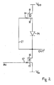
- FIG. 2 shows a current-limited inverter circuit that is suitable to provide an output stage of the input buffer.
- the D-mode transistor D in the inverter circuit of FIG. 2 will be referred to as feedback transistor and the E-mode transistor E as input transistor.
- the source 15 of the input transistor E is connected to ground or the lower potential V SS of a supply voltage.
- the drain 16 of the input transistor E is provided for an output signal OUT.
- the gate 17 of the input transistor E is provided for an input signal IN, which can be the output signal of the differential entry stage or of at least one further stage that may be connected between the differential entry stage and the inverter circuit and can comprise, for instance, a logic circuit.
- the drain 16 of the input transistor E is connected via the feedback connection 21 with the gate 20 of the feedback transistor D.
- the drain 19 of the feedback transistor D is connected to the higher potential V DD of the supply voltage.
- the drain 16 of the input transistor E is connected with the source 18 of the feedback transistor D via a component generating a voltage drop.
- This component can be formed by gate-source junctions of further E-mode transistors or, as shown in FIG. 2 , by a further diode 14 of a further transistor, which may be a bipolar or heterobipolar transistor.
- the use of a further diode 14 in the current-limiter of the inverter circuit may be advantageous in view of the requirements of circuit components that are driven by the output stage.
- the feedback transistor D, the component generating a voltage drop 14, and the feedback connection 21 are the current limiter of the inverter circuit. The operation of this circuit is as follows.
- the component that generates the voltage drop 14 is dimensioned in such a manner that the voltage drop causes the feedback transistor D to be switched to its sub-threshold region (the gate-source voltage of the feedback transistor D being comparable to the threshold voltage). Consequently, the current flowing through the feedback transistor D is very low, while the voltage level at the drain 16 of the input transistor E is essentially on ground level (V SS ). Thus the high input signal IN is transformed into a low output signal OUT.
- the gate-source voltage of the input transistor E When a low voltage level is applied to the gate 17 of the input transistor E, the gate-source voltage of the input transistor E is below its threshold voltage, so that the input transistor E is non-conducting, and almost no current flows through the source-drain path of the input transistor E.
- the only current through the feedback transistor D and the input transistor E is a very small current through the output OUT.
- the component that generates the voltage drop 14 is dimensioned in such a manner that the voltage drop is low enough for the negative gate-source voltage of the feedback transistor D to be above the more negative threshold voltage. Therefore the feedback transistor D is conducting between source and drain, and the corresponding switch is closed. Accordingly, the output signal OUT is on a high level.
- the low input signal IN is transformed into a high output signal OUT, and this circuit therefore functions as a current-limited inverter.
- the low-current input buffer is suitable to convert CMOS level inputs to levels usable in GaAs circuits, this without requiring high currents. Furthermore, an overall enable function can easily be implemented.
- the transistors that are applied in the input buffer can all be devices of a BiFET technology in GaAs.
- the input buffer is particularly useful to drive a high-impedance load, like a depletion-mode FET or a depletion-mode P-HEMT.
Landscapes
- Engineering & Computer Science (AREA)
- Computer Hardware Design (AREA)
- Physics & Mathematics (AREA)
- Computing Systems (AREA)
- General Engineering & Computer Science (AREA)
- Mathematical Physics (AREA)
- Logic Circuits (AREA)
Abstract
Description
- This invention relates to low-current input buffers compatible with CMOS levels for applications in GaAs technology.
- Conventional logic circuits in GaAs technology use a transistor in combination with a large resistor. These circuits require both high input drive currents and high currents in the on-state because of the required voltage drop over the resistor. Furthermore, the resistor occupies a large chip area to provide the desired large resistance.
- It is an object of this invention to present a low-current input buffer which is compatible with CMOS levels and can be realized in GaAs technology.
- This object is achieved with the low-current input buffer according to claim 1. Further embodiments and variants can be derived from the depending claims.
- The low-current input buffer comprises a current-limited differential entry stage comparing an input signal to a reference voltage, which is generated by a current-limited transistor or diode configuration. The current-limited components of the input buffer are each provided with a current limiter and can be realized in GaAs technology. Various components available in this technology, especially merged or stacked FET-HBT integration schemes, often called BiFET or BiHEMT and containing both HBT and FET or P-HEMT devices on a single GaAs substrate, can be used in the circuit.
- The low-current input buffer makes use of E-mode (enhancement) and D-mode (depletion) transistors comprising a source, a drain and a gate controlling a channel between source and drain and further comprising a gate-source junction and/or a gate-drain junction. The transistors can be symmetric with respect to source and drain, so that a gate-source junction and a similar gate-drain junction are available. An E-mode transistor is conducting between the source and the drain if the gate-source voltage is larger positive than a positive threshold voltage and is not conducting between the source and the drain if the gain-source voltage is lower. A D-mode transistor is not conducting between the source and the drain if the gate-source voltage is more negative than a negative threshold voltage and is conducting between the source and the drain in the case of a gate-source voltage above the threshold voltage (less negative, zero or positive).
- A current limiter is connected between a current-limited component and a voltage level of a supply voltage. The current limiters comprise a D-mode feedback transistor and a feedback loop connecting the source of the D-mode feedback transistor to the gate of the D-mode feedback transistor via a component that generates a voltage drop. The component generating a voltage drop can comprise at least one E-mode transistor or a diode formed by the basis and the emitter or collector of a bipolar transistor or a heterobipolar transistor.
- The differential entry stage can be provided with a current source that is connected between the differential circuit and a voltage level of the supply voltage. The current source can be used within a current mirror to connect the differential entry stage with a current-limited control circuit. The control circuit may be used to switch the whole input buffer on and off.
- In an embodiment of the low-current input buffer, the differential entry stage is formed with a first E-mode transistor, a second E-mode transistor, a first D-mode transistor and a second D-mode transistor. The gate of the first E-mode transistor is provided as input, and the drain of the second E-mode transistor is provided as output. The drain of the first E-mode transistor is connected to the source of the first D-mode transistor. The gate of the second E-mode transistor is connected to a component generating a reference voltage. A component generating a voltage drop is connected between the drain of the second E-mode transistor and the source of the second D-mode transistor. The drain of the second E-mode transistor is connected with the gates of the first and second D-mode transistors. The drains of the first and second D-mode transistors are to be connected to a high voltage level VDD of a supply voltage, and the sources of the first and second E-mode transistors are connected to a current source. The current source can be provided by a third E-mode transistor, the source of which is connected to a low voltage level of the supply voltage and the drain of which is connected to the sources of the first and second E-mode transistors. The gate of the third E-mode transistor may be addressed by a control circuit.
- In a further embodiment, a current mirror is connected to the sources of the first and second E-mode transistors. The current mirror comprises a current source, which can be provided, for instance, by a third E-mode transistor, the source of which is connected to a low voltage level of the supply voltage and the drain of which is connected to the sources of the first and second E-mode transistors. The current mirror further comprises a current-limited control circuit connected to the gate of the third E-mode transistor. The control circuit comprises a reference current source, which can be provided, for instance, by a further E-mode transistor, the source of which is connected to the low voltage level of the supply voltage and the drain of which is short-circuited to its gate. The drain is also connected to a high level of the supply voltage via an optional voltage shift member and a current limiter. The voltage shift member can be provided, for instance, by a second further E-mode transistor, the source of which is connected to the drain of the first further E-mode transistor and the drain of which is short-circuited to its gate. The current limiter comprises a further D-mode feedback transistor and a feedback loop connecting the source of the further D-mode feedback transistor to the gate of the further D-mode feedback transistor via a component that generates a voltage drop. If a voltage shift member is formed by a second further E-mode transistor, the drain of the second further E-mode transistor is connected to the gate of the further D-mode feedback transistor. Otherwise the reference current source, particularly the drain of its further E-mode transistor, is connected to the gate of the further D-mode feedback transistor. The high level of the voltage can be the voltage level that is to be connected to the drains of the first and second D-mode transistors. The connection of the control circuit to the high level of the voltage can be made switchable, similar to the application of an enable voltage which switches the entire circuit on and off.
- In a further embodiment of the low-current input buffer, a current-limited inverter circuit is used as an output stage.
- The output signal of the differential entry stage described above or the output signal of a successive circuit stage is used as an input signal of the current-limited inverter circuit. The inverter circuit is provided with a current-limiter comprising a D-mode feedback transistor and a feedback loop connecting the source of the D-mode feedback transistor to the gate of the D-mode feedback transistor via a component that generates a voltage drop. The inverter circuit can further comprise an E-mode input transistor. The component that generates a voltage drop is connected between the drain of the E-mode input transistor and the source of the D-mode feedback transistor. The drain of the input transistor is also connected to the gate of the feedback transistor. The supply voltage is to be applied to the source of the input transistor and the drain of the feedback transistor, the drain of the feedback transistor being supplied with the high voltage level of the supply voltage. The gate of the input transistor is provided for an input signal, and the drain of the input transistor is provided for an output signal. The component that generates a voltage drop can advantageously be provided by a diode of a bipolar transistor or a heterobipolar transistor. An inverter circuit of this latter design is especially suitable as output stage of the input buffer to drive a high-impedance load like a depletion-mode FET or a depletion-mode P-HEMT, for example.
- In a further embodiment, the reference voltage is generated by a current-limited component that generates a voltage drop. It is switched between a voltage level of the supply voltage and a further current-limiter, the current-limiter comprising a D-mode feedback transistor, a feedback loop and a further component generating a voltage drop in the feedback loop.
- These and other objects, features and advantages of the low-current input buffer will become apparent from the following detailed description of examples in conjunction with the appended figures.
- FIG. 1
- shows a circuit diagram of an embodiment of the low-current input buffer.
- FIG. 2
- shows a circuit diagram of a current-limited inverter circuit applied as output stage of a further embodiment of the input buffer.
-
FIG. 1 shows a circuit diagram of an embodiment of the low-current input buffer. The transistors appearing in the circuit are a kind of field-effect transistors comprising source, drain and gate as well as a diode formed by a junction between gate and source or drain. The transistors are therefore represented in the circuit diagram by symbols used for n-channel JFETS, but other types of transistors having a comparable structure can be used as well. In the examples shown in the figures, the gate-source junctions of the transistors are used. - The transistors designated with a D (D-mode, depletion mode) are characterized by a negative threshold voltage. If a gate-source voltage is applied that is larger negative (which means negative and of a larger absolute value) than the negative threshold voltage, the source-drain path through the channel of the transistor is non-conducting. If the transistor is considered as a switch, the switch is open if the gate-source voltage is larger negative than the threshold voltage. This type of transistor may therefore be characterized as "normally-on". If the gate-source voltage is not as negative as the threshold voltage or if it is zero or positive, the source-drain path is conducting: the switch is closed.
- The E-mode (enhancement mode) transistor is characterized by a positive threshold voltage. The E-mode transistors are conducting between source and drain if the gate-source voltage is larger than the positive threshold voltage: the switch is closed. If the gate-source voltage is lower than the positive threshold voltage or if it is zero or negative, the transistor is non-conducting: the switch is open. Thus, the E-mode transistors can be characterized as "normally-off".
- The differential entry stage of the embodiment of the low-current input buffer shown in
FIG. 1 comprises a first E-mode transistor E1, a second E-mode transistor E2, a first D-mode transistor D1, and a second D-mode transistor D2. An optional current source is provided by means of a third E-mode transistor E3. Thesource 32 of the third E-mode transistor E3 is connected to ground or to a low voltage level VSS of the supply voltage. Thedrain 33 of the third E-mode transistor E3 is connected to the source 1 of the first E-mode transistor E1 and to thesource 4 of the second E-mode transistors E2. The drain 2 of the first E-mode transistor E1 is connected to the source 7 of the first D-mode transistor D1. The drain 5 of the second E-mode transistor E2 is connected to thesource 10 of the second D-mode transistor D2. - The component that generates a voltage drop in the current limiter can be provided by a gate-source junction or by a gate-drain junction of a further E-mode transistor. The junctions of the further E-mode transistor may be switched in parallel by connecting source and drain. Gate-source junctions or gate-drain junctions of further E-mode transistors can be connected in series to obtain the adequate value of the voltage drop. Instead, the component that generates a voltage drop can be provided by a diode, especially a diode formed by the basis and the emitter or collector of a bipolar or heterobipolar transistor. In the embodiment shown in
FIG. 1 , the component that generates a voltage drop comprises the gate-source junctions of a fourth E-mode transistor E4 and a fifth E-mode transistor E5, connected in series between thesource 10 of the second D-mode transistor D2 and the drain 5 of the second E-mode transistor E2. - The
gate 12 of the second D-mode transistor D2 is connected to the gate 9 of the first D-mode transistor D1. The drain 8 of the first D-mode transistor D1 and the drain 11 of the second D-mode transistor D2 are connected to a high voltage level VDD of the supply voltage. Thegate 3 of the first E-mode transistor E1 is provided for an input signal IN, and the drain 5 of the second E-mode transistor E2 is provided for an output signal OUT. The reference voltage Vref is applied to thegate 6 of the second E-mode transistor E2. - The configuration generating the reference voltage Vref comprises gate-source junctions of a sixth E-mode transistor E6 and of a seventh E-mode transistor E7, the gate-source junctions being connected in series. Instead, only one gate-source junction may be used, or the number of gate-source junctions of E-mode transistors connected in series may be larger than two. The gate-source junctions and the gate-drain junctions may also be switched parallel. Instead of gate-source or gate-drain junctions of E-mode transistors, other configurations of diodes, particularly diodes of bipolar or heterobipolar transistors, and/or transistors can be used to generate the desired reference voltage.
- The configuration generating the reference voltage Vref is switched between a further current limiter and the low level VSS of the supply voltage. The further current limiter comprises a third D-mode transistor D3, a further component generating a voltage drop, and a
feedback connection 23. The further component generating a voltage drop comprises an eighth E-mode transistor E8 and a ninth E-mode transistor E9 having their gate-source junctions connected in series. The component generating a voltage drop may be varied according to the above description of the current limiter of the differential entry stage. - The current source provided by the third E-mode transistor E3 may be part of a current mirror comprising the third E-mode transistor E3 and a tenth E-mode transistor (E10). The
gate 34 of the third E-mode transistor E3 is connected to thegate 37 of the tenth E-mode transistor E10 by means of afurther connection 30. Thegate 37 and thedrain 36 of the tenth E-mode transistor E10 are short-circuited by means of afurther connection 31. Thedrain 36 of the tenth E-mode transistor E10 is connected to a further current limiter. This further current limiter comprises a fourth D-mode transistor D4, a further component generating a voltage drop, which is the gate-source junction of an eleventh E-mode transistor E11, and afurther feedback connection 22. The component generating a voltage drop may be varied according to the above description of the current limiter of the differential entry stage. Thefeedback connection 22 connects the component generating a voltage drop with thegate 29 of the fourth D-mode transistor D4. Thesource 27 of the fourth D-mode transistor D4 is connected to the component generating the voltage drop, and thedrain 28 of the fourth D-mode transistor D4 is connected to a voltage level Ven of the supply voltage, which may be the high voltage level VDD. If thedrain 28 of the fourth D-mode transistor D4 is connected in a switchable manner to the voltage level, especially to an enable voltage Ven provided in the circuitry, the input buffer can be switched on and off. - A voltage shift member can be connected between the
drain 36 of the tenth E-mode transistor E10 and the current limiter comprising the eleventh E-mode transistor E11 and the fourth D-mode transistor D4. In the embodiment shown inFIG. 1 , the voltage shift member is a twelfth E-mode transistor E12. Thedrain 36 of the tenth E-mode transistor E10 is connected to thesource 38 of the twelfth E-mode transistor E12, and the drain 39 of the twelfth E-mode transistor E12 is short-circuited to itsgate 40 and connected to thefeedback connection 22. -
FIG. 2 shows a current-limited inverter circuit that is suitable to provide an output stage of the input buffer. In the following, the D-mode transistor D in the inverter circuit ofFIG. 2 will be referred to as feedback transistor and the E-mode transistor E as input transistor. Thesource 15 of the input transistor E is connected to ground or the lower potential VSS of a supply voltage. Thedrain 16 of the input transistor E is provided for an output signal OUT. Thegate 17 of the input transistor E is provided for an input signal IN, which can be the output signal of the differential entry stage or of at least one further stage that may be connected between the differential entry stage and the inverter circuit and can comprise, for instance, a logic circuit. Thedrain 16 of the input transistor E is connected via thefeedback connection 21 with thegate 20 of the feedback transistor D. Thedrain 19 of the feedback transistor D is connected to the higher potential VDD of the supply voltage. Thedrain 16 of the input transistor E is connected with thesource 18 of the feedback transistor D via a component generating a voltage drop. This component can be formed by gate-source junctions of further E-mode transistors or, as shown inFIG. 2 , by afurther diode 14 of a further transistor, which may be a bipolar or heterobipolar transistor. The use of afurther diode 14 in the current-limiter of the inverter circuit may be advantageous in view of the requirements of circuit components that are driven by the output stage. The feedback transistor D, the component generating avoltage drop 14, and thefeedback connection 21 are the current limiter of the inverter circuit. The operation of this circuit is as follows. - When a high voltage level is applied to the
gate 17 of the input transistor E, which means a high logical input signal IN, this voltage will drive the input transistor E into a conducting mode. The corresponding switch between source and drain is therefore closed, and the ground potential VSS is connected with thegate 20 of the feedback transistor D. The voltage of the input signal IN only needs to be high enough for the gate-source voltage of the input transistor E to be larger than the threshold voltage of this transistor. The voltage over the component that generates thevoltage drop 14 makes a current flow through the feedback transistor D and the input transistor E, thus causing a voltage drop, so that the voltage level at thegate 20 of the feedback transistor D is lower than the voltage level at thesource 18 of the feedback transistor D. The component that generates thevoltage drop 14 is dimensioned in such a manner that the voltage drop causes the feedback transistor D to be switched to its sub-threshold region (the gate-source voltage of the feedback transistor D being comparable to the threshold voltage). Consequently, the current flowing through the feedback transistor D is very low, while the voltage level at thedrain 16 of the input transistor E is essentially on ground level (VSS). Thus the high input signal IN is transformed into a low output signal OUT. - When a low voltage level is applied to the
gate 17 of the input transistor E, the gate-source voltage of the input transistor E is below its threshold voltage, so that the input transistor E is non-conducting, and almost no current flows through the source-drain path of the input transistor E. The only current through the feedback transistor D and the input transistor E is a very small current through the output OUT. The component that generates thevoltage drop 14 is dimensioned in such a manner that the voltage drop is low enough for the negative gate-source voltage of the feedback transistor D to be above the more negative threshold voltage. Therefore the feedback transistor D is conducting between source and drain, and the corresponding switch is closed. Accordingly, the output signal OUT is on a high level. Thus the low input signal IN is transformed into a high output signal OUT, and this circuit therefore functions as a current-limited inverter. - The low-current input buffer is suitable to convert CMOS level inputs to levels usable in GaAs circuits, this without requiring high currents. Furthermore, an overall enable function can easily be implemented. The transistors that are applied in the input buffer can all be devices of a BiFET technology in GaAs. The input buffer is particularly useful to drive a high-impedance load, like a depletion-mode FET or a depletion-mode P-HEMT.
-
- 1
- source of the first E-mode transistor
- 2
- drain of the first E-mode transistor
- 3
- gate of the first E-mode transistor
- 4
- source of the second E-mode transistor
- 5
- drain of the second E-mode transistor
- 6
- gate of the second E-mode transistor
- 7
- source of the first D-mode transistor
- 8
- drain of the first D-mode transistor
- 9
- gate of the first D-mode transistor
- 10
- source of the second D-mode transistor
- 11
- drain of the second D-mode transistor
- 12
- gate of the second D-mode transistor
- 13
- feedback connection
- 14
- further diode
- 15
- source of the input transistor
- 16
- drain of the input transistor
- 17
- gate of the input transistor
- 18
- source of the feedback transistor
- 19
- drain of the feedback transistor
- 20
- gate of the feedback transistor
- 21
- feedback connection
- 22
- feedback connection
- 23
- feedback connection
- 24
- source of the third D-mode transistor
- 25
- drain of the third D-mode transistor
- 26
- gate of the third D-mode transistor
- 27
- source of the fourth D-mode transistor
- 28
- drain of the fourth D-mode transistor
- 29
- gate of the fourth D-mode transistor
- 30
- connection
- 31
- connection
- 32
- source of the third E-mode transistor
- 33
- drain of the third E-mode transistor
- 34
- gate of the third E-mode transistor
- 35
- source of the tenth E-mode transistor
- 36
- drain of the tenth E-mode transistor
- 37
- gate of the tenth E-mode transistor
- 38
- source of the twelfth E-mode transistor
- 39
- drain of the twelfth E-mode transistor
- 40
- gate of the twelfth E-mode transistor
- D
- feedback transistor
- D1
- first D-mode transistor
- D2
- second D-mode transistor
- D3
- third D-mode transistor
- D4
- fourth D-mode transistor
- E
- input transistor
- E1
- first E-mode transistor
- E2
- second E-mode transistor
- E3
- third E-mode transistor
- E4
- fourth E-mode transistor
- E5
- fifth E-mode transistor
- E6
- sixth E-mode transistor
- E7
- seventh E-mode transistor
- E8
- eighth E-mode transistor
- E9
- ninth E-mode transistor
- E10
- tenth E-mode transistor
- E11
- eleventh E-mode transistor
- E12
- twelfth E-mode transistor
- IN
- input
- OUT
- output
- VDD
- high potential level of a supply voltage
- VSS
- low potential level of a supply voltage
Claims (15)
- Low-current input buffer, comprising:- a current-limited differential entry stage comparing an input signal (IN) to a reference voltage (Vref) and- a current-limited transistor or diode configuration (E6, E7) generating the reference voltage,- current limiters being provided for the differential entry stage and for the configuration generating the reference voltage, each current limiter comprising- a D-mode feedback transistor (D2; D3) having a source (10; 24), a drain (11, 25), a gate (12; 26) that is provided to control a channel between the source and the drain, and a gate-source junction, the D-mode transistor not conducting between the source and the drain if a gate-source voltage that is applied between the gate and the source is larger negative than a negative threshold voltage, and conducting between the source and the drain else, and- a feedback connection (13; 23) connecting the source of the D-mode feedback transistor to the gate of the D-mode feedback transistor via a component that generates a voltage drop (E4, E5; E8, E9).
- The low-current input buffer of claim 1, further comprising:the configuration generating the reference voltage (Vref) comprising a gate-source junction of an E-mode transistor (E6, E7) having a source, a drain, and a gate that is provided to control a channel between the source and the drain, the E-mode transistor conducting between the source and the drain if a gate-source voltage that is applied between the gate and the source is larger positive than a positive threshold voltage, and not conducting between the source and the drain else.
- The low-current input buffer of claim 1, further comprising:the configuration generating the reference voltage (Vref) comprising gate-source junctions of at least two E-mode transistors (E6, E7) having a source, a drain, and a gate that is provided to control a channel between the source and the drain, the E-mode transistors conducting between the source and the drain if a gate-source voltage that is applied between the gate and the source is larger positive than a positive threshold voltage, and not conducting between the source and the drain else, andthe gate-source junctions being connected in series.
- The low-current input buffer according to one of claims 1 to 3, further comprising:in the differential entry stage- a first E-mode transistor (E1) and a second E-mode transistor (E2) each having a source (1, 4), a drain (2, 5), a gate (3, 6) that is provided to control a channel between the source and the drain, and a gate-source junction, each E-mode transistor conducting between the source and the drain if a gate-source voltage that is applied between the gate and the source is larger positive than a positive threshold voltage, and not conducting between the source and the drain else,- a first D-mode transistor (D1) and a second D-mode transistor (D2) each having a source (7, 10), a drain (8, 11), a gate (9, 12) that is provided to control a channel between the source and the drain, and a gate-source junction, each D-mode transistor not conducting between the source and the drain if a gate-source voltage that is applied between the gate and the source is larger negative than a negative threshold voltage, and conducting between the source and the drain else,- the drain (2) of the first E-mode transistor being connected to the source (7) of the first D-mode transistor,- the drain (5) of the second E-mode transistor being connected to the source (10) of the second D-mode transistor,- the second D-mode transistor being provided as the D-mode feedback transistor of the current limiter of the differential entry stage,- the component that generates a voltage drop (E4, E5) being connected between the drain of the second E-mode transistor and the source of the second D-mode transistor,- the gate of the second D-mode transistor being connected to the gate of the first D-mode transistor,- the sources (1, 4) of the first and second E-mode transistors being provided to be connected to a first voltage level (VSS) of the supply voltage,- the drains (8, 11) of the first and second D-mode transistors being provided to be connected to a second voltage level (VDD) of a supply voltage,- the gate (3) of the first E-mode transistor being provided for an application of an input signal (IN),- the gate (6) of the second E-mode transistor being provided for an application of the reference voltage (Vref), and- the drain (5) of the second E-mode transistor being provided for an output signal (OUT).
- The low-current input buffer of claim 4, further comprising:- a current mirror comprising a third E-mode transistor (E3) and a further E-mode transistor (E10), each E-mode transistor having a source, a drain, a gate that is provided to control a channel between the source and the drain, and a gate-source junction, each E-mode transistor conducting between the source and the drain if a gate-source voltage that is applied between the gate and the source is larger positive than a positive threshold voltage, and not conducting between the source and the drain else,- the source (32) of the third E-mode transistor being provided to be connected to the first voltage level (VSS) of the supply voltage,- the drain (33) of the third E-mode transistor being connected to the sources (1, 4) of the first and second E-mode transistors (E1, E2),- the gate (34) of the third E-mode transistor being connected to the gate (37) of the further E-mode transistor,- the gate (37) and the drain (36) of the further E-mode transistor being short-circuited, and- the drain of the further E-mode transistor being connected to a further current limiter (D4, E11).
- The low-current input buffer of claim 5, further comprising:the drain (36) of the further E-mode transistor (E10) being connected to the further current limiter (D4, E11) via a voltage shift member (E10), the voltage shift member being provided by a second further E-mode transistor (E12) having a gate-source junction and having a gate and a drain, which are short-circuited.
- The low-current input buffer according to one of claims 5 or 6, further comprising:the further current limiter (D4, E11) of the current mirror being connected to a switchable voltage level (Ven) provided to switch the input buffer on and off.
- The low-current input buffer according to one of claims 1 to 7, wherein
the component that generates a voltage drop (E4, E5; E8, E9; E11) in a current limiter comprises a gate-source junction of a further E-mode transistor. - The low-current input buffer according to one of claims 1 to 7, wherein
the component that generates a voltage drop (E4, E5; E8, E9) in a current limiter comprises at least two gate-source junctions of further E-mode transistors, the gate-source junctions being connected in series. - The low-current input buffer according to one of claims 1 to 9, further comprising:a current-limited inverter circuit having an input, an output (OUT) of the differential entry stage being connected to the input of the current-limited inverter circuit.
- The low-current input buffer of claim 10, wherein the current-limited inverter circuit further comprises:- an input transistor (E) and a feedback transistor (D), each having a source (15; 18), a drain (16; 19) and a gate (17; 20) that is provided to control a channel between the source and the drain, and each having a gate-source junction,- the input transistor conducting between the source and the drain if a gate-source voltage that is applied between the gate and the source is larger positive than a positive threshold voltage, and not conducting between the source and the drain else,- the feedback transistor not conducting between the source and the drain if a gate-source voltage that is applied between the gate and the source is larger negative than a negative threshold voltage, and conducting between the source and the drain else,- a component that generates a voltage drop (14) between the source (18) of the feedback transistor and the drain (16) of the input transistor,- a feedback connection (21) between the drain (16) of the input transistor and the gate (20) of the feedback transistor,- the source (15) of the input transistor being provided to be connected to a first voltage level (VSS) of a supply voltage,- the drain (19) of the feedback transistor being provided to be connected to a second voltage level (VDD) of the supply voltage.
- The low-current input buffer of claim 11, further comprising:a further transistor, which is a bipolar transistor or a heterobipolar transistor, andthe component that generates a voltage drop (14) of the inverter circuit comprising a diode of the further transistor.
- The low-current input buffer according to one of claims 1 to 12, wherein
the transistors are devices of a BiFET technology in GaAs. - The low-current input buffer according to one of claims 1 to 13, wherein
an output signal (OUT) of the input buffer is provided to drive a high-impedance load. - The low-current input buffer of claim 14, wherein
the high-impedance load is a depletion-mode FET or a depletion-mode P-HEMT.
Priority Applications (4)
| Application Number | Priority Date | Filing Date | Title |
|---|---|---|---|
| EP09163406.3A EP2270946B1 (en) | 2009-06-22 | 2009-06-22 | Low-current input buffer |
| JP2012516687A JP5442861B2 (en) | 2009-06-22 | 2010-06-21 | Low current input buffer |
| US13/322,367 US8436663B2 (en) | 2009-06-22 | 2010-06-21 | Low-current input buffer |
| PCT/EP2010/058743 WO2010149629A1 (en) | 2009-06-22 | 2010-06-21 | Low-current input buffer |
Applications Claiming Priority (1)
| Application Number | Priority Date | Filing Date | Title |
|---|---|---|---|
| EP09163406.3A EP2270946B1 (en) | 2009-06-22 | 2009-06-22 | Low-current input buffer |
Publications (2)
| Publication Number | Publication Date |
|---|---|
| EP2270946A1 true EP2270946A1 (en) | 2011-01-05 |
| EP2270946B1 EP2270946B1 (en) | 2014-04-09 |
Family
ID=41426288
Family Applications (1)
| Application Number | Title | Priority Date | Filing Date |
|---|---|---|---|
| EP09163406.3A Active EP2270946B1 (en) | 2009-06-22 | 2009-06-22 | Low-current input buffer |
Country Status (4)
| Country | Link |
|---|---|
| US (1) | US8436663B2 (en) |
| EP (1) | EP2270946B1 (en) |
| JP (1) | JP5442861B2 (en) |
| WO (1) | WO2010149629A1 (en) |
Cited By (1)
| Publication number | Priority date | Publication date | Assignee | Title |
|---|---|---|---|---|
| CN104521202A (en) * | 2012-06-12 | 2015-04-15 | 密执安州立大学董事会 | Ultra-low-power radio for short-range communication |
Families Citing this family (2)
| Publication number | Priority date | Publication date | Assignee | Title |
|---|---|---|---|---|
| US9806720B1 (en) * | 2016-10-07 | 2017-10-31 | Analog Devices Global | Compound semiconductor based inverter |
| CN117200776B (en) * | 2023-09-22 | 2024-03-08 | 江苏帝奥微电子股份有限公司 | Depletion type switch circuit architecture for improving unidirectional or bidirectional isolation signals |
Citations (2)
| Publication number | Priority date | Publication date | Assignee | Title |
|---|---|---|---|---|
| JPH02280413A (en) * | 1989-04-20 | 1990-11-16 | Sharp Corp | Basic logic circuit |
| US4978904A (en) | 1987-12-15 | 1990-12-18 | Gazelle Microcircuits, Inc. | Circuit for generating reference voltage and reference current |
Family Cites Families (7)
| Publication number | Priority date | Publication date | Assignee | Title |
|---|---|---|---|---|
| JPS5211199B1 (en) | 1970-05-27 | 1977-03-29 | ||
| US3775693A (en) | 1971-11-29 | 1973-11-27 | Moskek Co | Mosfet logic inverter for integrated circuits |
| FR2330221A1 (en) | 1973-07-10 | 1977-05-27 | Thomson Csf | IMPROVEMENT OF LOGIC VOLTAGE INVERTER CIRCUITS |
| JPS61161020A (en) | 1985-01-08 | 1986-07-21 | Mitsubishi Electric Corp | Nmos inverting circuit |
| US5091662A (en) * | 1989-05-23 | 1992-02-25 | Texas Instruments Incorporated | High-speed low-power supply-independent TTL compatible input buffer |
| JP2852679B2 (en) | 1989-09-01 | 1999-02-03 | 富士通株式会社 | Semiconductor device and manufacturing method thereof |
| US5910737A (en) * | 1997-06-30 | 1999-06-08 | Delco Electronics Corporation | Input buffer circuit with differential input thresholds operable with high common mode input voltages |
-
2009
- 2009-06-22 EP EP09163406.3A patent/EP2270946B1/en active Active
-
2010
- 2010-06-21 WO PCT/EP2010/058743 patent/WO2010149629A1/en not_active Ceased
- 2010-06-21 JP JP2012516687A patent/JP5442861B2/en active Active
- 2010-06-21 US US13/322,367 patent/US8436663B2/en not_active Expired - Fee Related
Patent Citations (2)
| Publication number | Priority date | Publication date | Assignee | Title |
|---|---|---|---|---|
| US4978904A (en) | 1987-12-15 | 1990-12-18 | Gazelle Microcircuits, Inc. | Circuit for generating reference voltage and reference current |
| JPH02280413A (en) * | 1989-04-20 | 1990-11-16 | Sharp Corp | Basic logic circuit |
Cited By (3)
| Publication number | Priority date | Publication date | Assignee | Title |
|---|---|---|---|---|
| CN104521202A (en) * | 2012-06-12 | 2015-04-15 | 密执安州立大学董事会 | Ultra-low-power radio for short-range communication |
| EP2870739A4 (en) * | 2012-06-12 | 2016-02-24 | Univ Michigan | ULTRA-BASS POWER RADIO FOR SHORT-TERM COMMUNICATION |
| CN104521202B (en) * | 2012-06-12 | 2017-06-09 | 密执安州立大学董事会 | For the ultra low power wireless device of junction service |
Also Published As
| Publication number | Publication date |
|---|---|
| JP5442861B2 (en) | 2014-03-12 |
| WO2010149629A1 (en) | 2010-12-29 |
| US8436663B2 (en) | 2013-05-07 |
| US20120112801A1 (en) | 2012-05-10 |
| EP2270946B1 (en) | 2014-04-09 |
| JP2012531158A (en) | 2012-12-06 |
Similar Documents
| Publication | Publication Date | Title |
|---|---|---|
| US20100283061A1 (en) | High temperature gate drivers for wide bandgap semiconductor power jfets and integrated circuits including the same | |
| JPS6113817A (en) | Electric circuit using metal semiconductor field effect transistor | |
| US6046622A (en) | Electronic analogue switch | |
| EP2270946B1 (en) | Low-current input buffer | |
| EP2264900B1 (en) | Low-current inverter circuit | |
| US5420527A (en) | Temperature and supply insensitive TTL or CMOS to 0/-5 V translator | |
| EP2264899B1 (en) | Low-current logic-gate circuit | |
| US20210211128A1 (en) | Gate Drive Apparatus and Control Method | |
| US5661411A (en) | Feedback controlled load logic circuit | |
| EP0282249A2 (en) | Logic circuit employing field effect transistor having junction with rectifying characteristic between gate and source | |
| JP2562831B2 (en) | Level conversion circuit | |
| WO2023177470A1 (en) | Common gate input circuit for iii/v d-mode buffered fet logic (bfl) | |
| US8686752B2 (en) | Low-current logic plus driver circuit | |
| US5087836A (en) | Electronic circuit including a parallel combination of an E-FET and a D-FET | |
| US20250309900A1 (en) | Logic gate circuit | |
| JP3086754B2 (en) | Semiconductor logic integrated circuit | |
| JP2545712B2 (en) | Gallium arsenide semiconductor integrated circuit | |
| JPH0311129B2 (en) | ||
| JPH04105420A (en) | Semiconductor integrated circuit | |
| CA1286733C (en) | Low power, high noise margin logic gates employing enhancement mode switching fets | |
| JPH07106948A (en) | Logical gate circuit | |
| JP2000036734A (en) | Interface conversion circuit |
Legal Events
| Date | Code | Title | Description |
|---|---|---|---|
| PUAI | Public reference made under article 153(3) epc to a published international application that has entered the european phase |
Free format text: ORIGINAL CODE: 0009012 |
|
| AK | Designated contracting states |
Kind code of ref document: A1 Designated state(s): AT BE BG CH CY CZ DE DK EE ES FI FR GB GR HR HU IE IS IT LI LT LU LV MC MK MT NL NO PL PT RO SE SI SK TR |
|
| AX | Request for extension of the european patent |
Extension state: AL BA RS |
|
| 17P | Request for examination filed |
Effective date: 20110601 |
|
| 17Q | First examination report despatched |
Effective date: 20110624 |
|
| GRAP | Despatch of communication of intention to grant a patent |
Free format text: ORIGINAL CODE: EPIDOSNIGR1 |
|
| INTG | Intention to grant announced |
Effective date: 20131126 |
|
| GRAS | Grant fee paid |
Free format text: ORIGINAL CODE: EPIDOSNIGR3 |
|
| GRAA | (expected) grant |
Free format text: ORIGINAL CODE: 0009210 |
|
| AK | Designated contracting states |
Kind code of ref document: B1 Designated state(s): AT BE BG CH CY CZ DE DK EE ES FI FR GB GR HR HU IE IS IT LI LT LU LV MC MK MT NL NO PL PT RO SE SI SK TR |
|
| REG | Reference to a national code |
Ref country code: GB Ref legal event code: FG4D |
|
| REG | Reference to a national code |
Ref country code: AT Ref legal event code: REF Ref document number: 661793 Country of ref document: AT Kind code of ref document: T Effective date: 20140415 Ref country code: CH Ref legal event code: EP |
|
| REG | Reference to a national code |
Ref country code: IE Ref legal event code: FG4D |
|
| REG | Reference to a national code |
Ref country code: DE Ref legal event code: R096 Ref document number: 602009023063 Country of ref document: DE Effective date: 20140522 |
|
| REG | Reference to a national code |
Ref country code: AT Ref legal event code: MK05 Ref document number: 661793 Country of ref document: AT Kind code of ref document: T Effective date: 20140409 |
|
| REG | Reference to a national code |
Ref country code: NL Ref legal event code: VDEP Effective date: 20140409 |
|
| REG | Reference to a national code |
Ref country code: LT Ref legal event code: MG4D |
|
| PG25 | Lapsed in a contracting state [announced via postgrant information from national office to epo] |
Ref country code: FI Free format text: LAPSE BECAUSE OF FAILURE TO SUBMIT A TRANSLATION OF THE DESCRIPTION OR TO PAY THE FEE WITHIN THE PRESCRIBED TIME-LIMIT Effective date: 20140409 Ref country code: IS Free format text: LAPSE BECAUSE OF FAILURE TO SUBMIT A TRANSLATION OF THE DESCRIPTION OR TO PAY THE FEE WITHIN THE PRESCRIBED TIME-LIMIT Effective date: 20140809 Ref country code: LT Free format text: LAPSE BECAUSE OF FAILURE TO SUBMIT A TRANSLATION OF THE DESCRIPTION OR TO PAY THE FEE WITHIN THE PRESCRIBED TIME-LIMIT Effective date: 20140409 Ref country code: NL Free format text: LAPSE BECAUSE OF FAILURE TO SUBMIT A TRANSLATION OF THE DESCRIPTION OR TO PAY THE FEE WITHIN THE PRESCRIBED TIME-LIMIT Effective date: 20140409 Ref country code: BG Free format text: LAPSE BECAUSE OF FAILURE TO SUBMIT A TRANSLATION OF THE DESCRIPTION OR TO PAY THE FEE WITHIN THE PRESCRIBED TIME-LIMIT Effective date: 20140709 Ref country code: GR Free format text: LAPSE BECAUSE OF FAILURE TO SUBMIT A TRANSLATION OF THE DESCRIPTION OR TO PAY THE FEE WITHIN THE PRESCRIBED TIME-LIMIT Effective date: 20140710 Ref country code: NO Free format text: LAPSE BECAUSE OF FAILURE TO SUBMIT A TRANSLATION OF THE DESCRIPTION OR TO PAY THE FEE WITHIN THE PRESCRIBED TIME-LIMIT Effective date: 20140709 |
|
| PG25 | Lapsed in a contracting state [announced via postgrant information from national office to epo] |
Ref country code: LV Free format text: LAPSE BECAUSE OF FAILURE TO SUBMIT A TRANSLATION OF THE DESCRIPTION OR TO PAY THE FEE WITHIN THE PRESCRIBED TIME-LIMIT Effective date: 20140409 Ref country code: SE Free format text: LAPSE BECAUSE OF FAILURE TO SUBMIT A TRANSLATION OF THE DESCRIPTION OR TO PAY THE FEE WITHIN THE PRESCRIBED TIME-LIMIT Effective date: 20140409 Ref country code: PL Free format text: LAPSE BECAUSE OF FAILURE TO SUBMIT A TRANSLATION OF THE DESCRIPTION OR TO PAY THE FEE WITHIN THE PRESCRIBED TIME-LIMIT Effective date: 20140409 Ref country code: ES Free format text: LAPSE BECAUSE OF FAILURE TO SUBMIT A TRANSLATION OF THE DESCRIPTION OR TO PAY THE FEE WITHIN THE PRESCRIBED TIME-LIMIT Effective date: 20140409 Ref country code: AT Free format text: LAPSE BECAUSE OF FAILURE TO SUBMIT A TRANSLATION OF THE DESCRIPTION OR TO PAY THE FEE WITHIN THE PRESCRIBED TIME-LIMIT Effective date: 20140409 Ref country code: HR Free format text: LAPSE BECAUSE OF FAILURE TO SUBMIT A TRANSLATION OF THE DESCRIPTION OR TO PAY THE FEE WITHIN THE PRESCRIBED TIME-LIMIT Effective date: 20140409 |
|
| PG25 | Lapsed in a contracting state [announced via postgrant information from national office to epo] |
Ref country code: PT Free format text: LAPSE BECAUSE OF FAILURE TO SUBMIT A TRANSLATION OF THE DESCRIPTION OR TO PAY THE FEE WITHIN THE PRESCRIBED TIME-LIMIT Effective date: 20140811 |
|
| REG | Reference to a national code |
Ref country code: DE Ref legal event code: R097 Ref document number: 602009023063 Country of ref document: DE |
|
| PG25 | Lapsed in a contracting state [announced via postgrant information from national office to epo] |
Ref country code: LU Free format text: LAPSE BECAUSE OF FAILURE TO SUBMIT A TRANSLATION OF THE DESCRIPTION OR TO PAY THE FEE WITHIN THE PRESCRIBED TIME-LIMIT Effective date: 20140622 Ref country code: MC Free format text: LAPSE BECAUSE OF FAILURE TO SUBMIT A TRANSLATION OF THE DESCRIPTION OR TO PAY THE FEE WITHIN THE PRESCRIBED TIME-LIMIT Effective date: 20140409 Ref country code: SK Free format text: LAPSE BECAUSE OF FAILURE TO SUBMIT A TRANSLATION OF THE DESCRIPTION OR TO PAY THE FEE WITHIN THE PRESCRIBED TIME-LIMIT Effective date: 20140409 Ref country code: RO Free format text: LAPSE BECAUSE OF FAILURE TO SUBMIT A TRANSLATION OF THE DESCRIPTION OR TO PAY THE FEE WITHIN THE PRESCRIBED TIME-LIMIT Effective date: 20140409 Ref country code: DK Free format text: LAPSE BECAUSE OF FAILURE TO SUBMIT A TRANSLATION OF THE DESCRIPTION OR TO PAY THE FEE WITHIN THE PRESCRIBED TIME-LIMIT Effective date: 20140409 Ref country code: CZ Free format text: LAPSE BECAUSE OF FAILURE TO SUBMIT A TRANSLATION OF THE DESCRIPTION OR TO PAY THE FEE WITHIN THE PRESCRIBED TIME-LIMIT Effective date: 20140409 Ref country code: EE Free format text: LAPSE BECAUSE OF FAILURE TO SUBMIT A TRANSLATION OF THE DESCRIPTION OR TO PAY THE FEE WITHIN THE PRESCRIBED TIME-LIMIT Effective date: 20140409 Ref country code: BE Free format text: LAPSE BECAUSE OF FAILURE TO SUBMIT A TRANSLATION OF THE DESCRIPTION OR TO PAY THE FEE WITHIN THE PRESCRIBED TIME-LIMIT Effective date: 20140409 |
|
| REG | Reference to a national code |
Ref country code: CH Ref legal event code: PL |
|
| PLBE | No opposition filed within time limit |
Free format text: ORIGINAL CODE: 0009261 |
|
| STAA | Information on the status of an ep patent application or granted ep patent |
Free format text: STATUS: NO OPPOSITION FILED WITHIN TIME LIMIT |
|
| 26N | No opposition filed |
Effective date: 20150112 |
|
| GBPC | Gb: european patent ceased through non-payment of renewal fee |
Effective date: 20140709 |
|
| REG | Reference to a national code |
Ref country code: IE Ref legal event code: MM4A |
|
| REG | Reference to a national code |
Ref country code: FR Ref legal event code: ST Effective date: 20150227 |
|
| PG25 | Lapsed in a contracting state [announced via postgrant information from national office to epo] |
Ref country code: IT Free format text: LAPSE BECAUSE OF FAILURE TO SUBMIT A TRANSLATION OF THE DESCRIPTION OR TO PAY THE FEE WITHIN THE PRESCRIBED TIME-LIMIT Effective date: 20140409 |
|
| REG | Reference to a national code |
Ref country code: DE Ref legal event code: R097 Ref document number: 602009023063 Country of ref document: DE Effective date: 20150112 |
|
| PG25 | Lapsed in a contracting state [announced via postgrant information from national office to epo] |
Ref country code: CH Free format text: LAPSE BECAUSE OF NON-PAYMENT OF DUE FEES Effective date: 20140630 Ref country code: IE Free format text: LAPSE BECAUSE OF NON-PAYMENT OF DUE FEES Effective date: 20140622 Ref country code: LI Free format text: LAPSE BECAUSE OF NON-PAYMENT OF DUE FEES Effective date: 20140630 |
|
| PG25 | Lapsed in a contracting state [announced via postgrant information from national office to epo] |
Ref country code: GB Free format text: LAPSE BECAUSE OF NON-PAYMENT OF DUE FEES Effective date: 20140709 Ref country code: FR Free format text: LAPSE BECAUSE OF NON-PAYMENT OF DUE FEES Effective date: 20140630 |
|
| PG25 | Lapsed in a contracting state [announced via postgrant information from national office to epo] |
Ref country code: SI Free format text: LAPSE BECAUSE OF FAILURE TO SUBMIT A TRANSLATION OF THE DESCRIPTION OR TO PAY THE FEE WITHIN THE PRESCRIBED TIME-LIMIT Effective date: 20140409 |
|
| PG25 | Lapsed in a contracting state [announced via postgrant information from national office to epo] |
Ref country code: MT Free format text: LAPSE BECAUSE OF FAILURE TO SUBMIT A TRANSLATION OF THE DESCRIPTION OR TO PAY THE FEE WITHIN THE PRESCRIBED TIME-LIMIT Effective date: 20140409 |
|
| PG25 | Lapsed in a contracting state [announced via postgrant information from national office to epo] |
Ref country code: CY Free format text: LAPSE BECAUSE OF FAILURE TO SUBMIT A TRANSLATION OF THE DESCRIPTION OR TO PAY THE FEE WITHIN THE PRESCRIBED TIME-LIMIT Effective date: 20140409 |
|
| PG25 | Lapsed in a contracting state [announced via postgrant information from national office to epo] |
Ref country code: HU Free format text: LAPSE BECAUSE OF FAILURE TO SUBMIT A TRANSLATION OF THE DESCRIPTION OR TO PAY THE FEE WITHIN THE PRESCRIBED TIME-LIMIT; INVALID AB INITIO Effective date: 20090622 Ref country code: TR Free format text: LAPSE BECAUSE OF FAILURE TO SUBMIT A TRANSLATION OF THE DESCRIPTION OR TO PAY THE FEE WITHIN THE PRESCRIBED TIME-LIMIT Effective date: 20140409 |
|
| REG | Reference to a national code |
Ref country code: DE Ref legal event code: R082 Ref document number: 602009023063 Country of ref document: DE Representative=s name: BARDEHLE PAGENBERG PARTNERSCHAFT MBB PATENTANW, DE Ref country code: DE Ref legal event code: R081 Ref document number: 602009023063 Country of ref document: DE Owner name: SNAPTRACK, INC., SAN DIEGO, US Free format text: FORMER OWNER: EPCOS AG, 81669 MUENCHEN, DE |
|
| PG25 | Lapsed in a contracting state [announced via postgrant information from national office to epo] |
Ref country code: MK Free format text: LAPSE BECAUSE OF FAILURE TO SUBMIT A TRANSLATION OF THE DESCRIPTION OR TO PAY THE FEE WITHIN THE PRESCRIBED TIME-LIMIT Effective date: 20140409 |
|
| PGFP | Annual fee paid to national office [announced via postgrant information from national office to epo] |
Ref country code: DE Payment date: 20250509 Year of fee payment: 17 |