EP2267795A2 - Avalanche photodiode - Google Patents
Avalanche photodiode Download PDFInfo
- Publication number
- EP2267795A2 EP2267795A2 EP10166949A EP10166949A EP2267795A2 EP 2267795 A2 EP2267795 A2 EP 2267795A2 EP 10166949 A EP10166949 A EP 10166949A EP 10166949 A EP10166949 A EP 10166949A EP 2267795 A2 EP2267795 A2 EP 2267795A2
- Authority
- EP
- European Patent Office
- Prior art keywords
- region
- doped
- highly
- substrate
- type semiconductor
- Prior art date
- Legal status (The legal status is an assumption and is not a legal conclusion. Google has not performed a legal analysis and makes no representation as to the accuracy of the status listed.)
- Withdrawn
Links
- 239000004065 semiconductor Substances 0.000 claims abstract description 43
- 239000000463 material Substances 0.000 claims abstract description 22
- 239000000758 substrate Substances 0.000 claims description 83
- 238000000034 method Methods 0.000 claims description 21
- 238000002513 implantation Methods 0.000 claims description 12
- XUIMIQQOPSSXEZ-UHFFFAOYSA-N Silicon Chemical compound [Si] XUIMIQQOPSSXEZ-UHFFFAOYSA-N 0.000 description 34
- 229910052710 silicon Inorganic materials 0.000 description 34
- 239000010703 silicon Substances 0.000 description 34
- 238000004519 manufacturing process Methods 0.000 description 14
- 239000006117 anti-reflective coating Substances 0.000 description 12
- 238000001514 detection method Methods 0.000 description 11
- 238000000151 deposition Methods 0.000 description 10
- 239000002019 doping agent Substances 0.000 description 10
- 238000000407 epitaxy Methods 0.000 description 10
- VYPSYNLAJGMNEJ-UHFFFAOYSA-N Silicium dioxide Chemical compound O=[Si]=O VYPSYNLAJGMNEJ-UHFFFAOYSA-N 0.000 description 8
- 230000008021 deposition Effects 0.000 description 8
- 239000003574 free electron Substances 0.000 description 7
- 230000005684 electric field Effects 0.000 description 5
- ZOXJGFHDIHLPTG-UHFFFAOYSA-N Boron Chemical compound [B] ZOXJGFHDIHLPTG-UHFFFAOYSA-N 0.000 description 4
- 229910052581 Si3N4 Inorganic materials 0.000 description 4
- 229910052782 aluminium Inorganic materials 0.000 description 4
- XAGFODPZIPBFFR-UHFFFAOYSA-N aluminium Chemical compound [Al] XAGFODPZIPBFFR-UHFFFAOYSA-N 0.000 description 4
- 229910052785 arsenic Inorganic materials 0.000 description 4
- RQNWIZPPADIBDY-UHFFFAOYSA-N arsenic atom Chemical compound [As] RQNWIZPPADIBDY-UHFFFAOYSA-N 0.000 description 4
- 239000004020 conductor Substances 0.000 description 4
- BHEPBYXIRTUNPN-UHFFFAOYSA-N hydridophosphorus(.) (triplet) Chemical compound [PH] BHEPBYXIRTUNPN-UHFFFAOYSA-N 0.000 description 4
- 239000007943 implant Substances 0.000 description 4
- 229910052738 indium Inorganic materials 0.000 description 4
- APFVFJFRJDLVQX-UHFFFAOYSA-N indium atom Chemical compound [In] APFVFJFRJDLVQX-UHFFFAOYSA-N 0.000 description 4
- 229910052751 metal Inorganic materials 0.000 description 4
- 239000002184 metal Substances 0.000 description 4
- 235000012239 silicon dioxide Nutrition 0.000 description 4
- 239000000377 silicon dioxide Substances 0.000 description 4
- HQVNEWCFYHHQES-UHFFFAOYSA-N silicon nitride Chemical compound N12[Si]34N5[Si]62N3[Si]51N64 HQVNEWCFYHHQES-UHFFFAOYSA-N 0.000 description 4
- 229910052796 boron Inorganic materials 0.000 description 3
- JBRZTFJDHDCESZ-UHFFFAOYSA-N AsGa Chemical compound [As]#[Ga] JBRZTFJDHDCESZ-UHFFFAOYSA-N 0.000 description 2
- RYGMFSIKBFXOCR-UHFFFAOYSA-N Copper Chemical compound [Cu] RYGMFSIKBFXOCR-UHFFFAOYSA-N 0.000 description 2
- 229910002601 GaN Inorganic materials 0.000 description 2
- 229910005540 GaP Inorganic materials 0.000 description 2
- 229910001218 Gallium arsenide Inorganic materials 0.000 description 2
- JMASRVWKEDWRBT-UHFFFAOYSA-N Gallium nitride Chemical compound [Ga]#N JMASRVWKEDWRBT-UHFFFAOYSA-N 0.000 description 2
- 229910000673 Indium arsenide Inorganic materials 0.000 description 2
- GPXJNWSHGFTCBW-UHFFFAOYSA-N Indium phosphide Chemical compound [In]#P GPXJNWSHGFTCBW-UHFFFAOYSA-N 0.000 description 2
- BQCADISMDOOEFD-UHFFFAOYSA-N Silver Chemical compound [Ag] BQCADISMDOOEFD-UHFFFAOYSA-N 0.000 description 2
- 230000004075 alteration Effects 0.000 description 2
- 238000000137 annealing Methods 0.000 description 2
- 238000013459 approach Methods 0.000 description 2
- 238000003491 array Methods 0.000 description 2
- NWAIGJYBQQYSPW-UHFFFAOYSA-N azanylidyneindigane Chemical compound [In]#N NWAIGJYBQQYSPW-UHFFFAOYSA-N 0.000 description 2
- 239000000969 carrier Substances 0.000 description 2
- 229910052802 copper Inorganic materials 0.000 description 2
- 239000010949 copper Substances 0.000 description 2
- 238000010586 diagram Methods 0.000 description 2
- 230000000694 effects Effects 0.000 description 2
- VTGARNNDLOTBET-UHFFFAOYSA-N gallium antimonide Chemical compound [Sb]#[Ga] VTGARNNDLOTBET-UHFFFAOYSA-N 0.000 description 2
- HZXMRANICFIONG-UHFFFAOYSA-N gallium phosphide Chemical compound [Ga]#P HZXMRANICFIONG-UHFFFAOYSA-N 0.000 description 2
- 229910052732 germanium Inorganic materials 0.000 description 2
- GNPVGFCGXDBREM-UHFFFAOYSA-N germanium atom Chemical compound [Ge] GNPVGFCGXDBREM-UHFFFAOYSA-N 0.000 description 2
- PCHJSUWPFVWCPO-UHFFFAOYSA-N gold Chemical compound [Au] PCHJSUWPFVWCPO-UHFFFAOYSA-N 0.000 description 2
- 229910052737 gold Inorganic materials 0.000 description 2
- 239000010931 gold Substances 0.000 description 2
- WPYVAWXEWQSOGY-UHFFFAOYSA-N indium antimonide Chemical compound [Sb]#[In] WPYVAWXEWQSOGY-UHFFFAOYSA-N 0.000 description 2
- RPQDHPTXJYYUPQ-UHFFFAOYSA-N indium arsenide Chemical compound [In]#[As] RPQDHPTXJYYUPQ-UHFFFAOYSA-N 0.000 description 2
- ORUIBWPALBXDOA-UHFFFAOYSA-L magnesium fluoride Chemical compound [F-].[F-].[Mg+2] ORUIBWPALBXDOA-UHFFFAOYSA-L 0.000 description 2
- 229910001635 magnesium fluoride Inorganic materials 0.000 description 2
- 238000012986 modification Methods 0.000 description 2
- 230000004048 modification Effects 0.000 description 2
- 230000003647 oxidation Effects 0.000 description 2
- 238000007254 oxidation reaction Methods 0.000 description 2
- 238000002161 passivation Methods 0.000 description 2
- 238000005240 physical vapour deposition Methods 0.000 description 2
- 238000000623 plasma-assisted chemical vapour deposition Methods 0.000 description 2
- 238000007747 plating Methods 0.000 description 2
- HBMJWWWQQXIZIP-UHFFFAOYSA-N silicon carbide Chemical compound [Si+]#[C-] HBMJWWWQQXIZIP-UHFFFAOYSA-N 0.000 description 2
- 229910010271 silicon carbide Inorganic materials 0.000 description 2
- 229910052709 silver Inorganic materials 0.000 description 2
- 239000004332 silver Substances 0.000 description 2
- 238000006467 substitution reaction Methods 0.000 description 2
- 238000001771 vacuum deposition Methods 0.000 description 2
- 230000001419 dependent effect Effects 0.000 description 1
- 229910044991 metal oxide Inorganic materials 0.000 description 1
- 150000004706 metal oxides Chemical class 0.000 description 1
- 230000005855 radiation Effects 0.000 description 1
- 238000005510 radiation hardening Methods 0.000 description 1
- 238000001429 visible spectrum Methods 0.000 description 1
Images

Classifications
-
- H—ELECTRICITY
- H10—SEMICONDUCTOR DEVICES; ELECTRIC SOLID-STATE DEVICES NOT OTHERWISE PROVIDED FOR
- H10F—INORGANIC SEMICONDUCTOR DEVICES SENSITIVE TO INFRARED RADIATION, LIGHT, ELECTROMAGNETIC RADIATION OF SHORTER WAVELENGTH OR CORPUSCULAR RADIATION
- H10F30/00—Individual radiation-sensitive semiconductor devices in which radiation controls the flow of current through the devices, e.g. photodetectors
- H10F30/20—Individual radiation-sensitive semiconductor devices in which radiation controls the flow of current through the devices, e.g. photodetectors the devices having potential barriers, e.g. phototransistors
- H10F30/21—Individual radiation-sensitive semiconductor devices in which radiation controls the flow of current through the devices, e.g. photodetectors the devices having potential barriers, e.g. phototransistors the devices being sensitive to infrared, visible or ultraviolet radiation
- H10F30/22—Individual radiation-sensitive semiconductor devices in which radiation controls the flow of current through the devices, e.g. photodetectors the devices having potential barriers, e.g. phototransistors the devices being sensitive to infrared, visible or ultraviolet radiation the devices having only one potential barrier, e.g. photodiodes
- H10F30/225—Individual radiation-sensitive semiconductor devices in which radiation controls the flow of current through the devices, e.g. photodetectors the devices having potential barriers, e.g. phototransistors the devices being sensitive to infrared, visible or ultraviolet radiation the devices having only one potential barrier, e.g. photodiodes the potential barrier working in avalanche mode, e.g. avalanche photodiodes
Definitions
- This disclosure relates in general to photodetection and more particularly to a photodetection system and method utilizing one or more avalanche photodiodes.
- Photodetector circuits e.g., focal plane arrays
- Photodetector circuits are utilized in various devices to sense incident light in the visible and non-visible spectra.
- Photodetector circuits typically consist of an array of photodiodes that generate a charge, current, or voltage in proportion to the light intensity received at the location of each detector pixel.
- APDs are photodetectors that may be regarded as photon-multipliers.
- APD typically 10 volts or more in silicon
- APDs show an internal current gain effect (a gain of approximately 10 or more) due to phenomenon known as impact ionization or the avalanche effect. Because of this large gain, APDs have found to be particularly useful in high-sensitivity photodetection.
- conventional APDs are often not suitable for "back-side" illuminated devices which may be required for certain photodetection applications, in particular large-format focal plane arrays.
- conventional APDs are known to multiply signal (i.e., incident light) as well as noise, which is often undesirable in high-sensitivity applications.
- a photodiode may include a first region comprising substantially intrinsic semiconductor material, the region having a first side and a second side opposite to the first side.
- the photodiode may also include a second region comprising highly-doped p-type semiconductor material formed proximate to the first side of the first region.
- the photodiode may additionally include a third region comprising highly-doped n-type semiconductor material formed proximate to the second side of the first region.
- the photodiode may further include a fourth region comprising (i) highly-doped p-type semiconductor formed between the first region and the third region, or (ii) highly-doped n-type semiconductor formed between the first region and the second region.
- Technical advantages of certain embodiments may include providing a photodiode with higher signal-to-noise ratio as compared with conventional photodiodes.
- FIGURES 1 through 4 of the drawings like numerals being used for like and corresponding parts of the various drawings.
- FIGURE 1 is a block diagram illustrating photodetection system 100, in accordance with embodiments of the present disclosure.
- photodetection system 100 may be a digital camera, video camera, or any other photographic device, image capturing device, and/or high-speed photon counting device.
- Photodetection system 100 may include detection device 120 and signal processing unit 140.
- Detection device 120 may be a focal plane array (FPA), active pixel sensor (APS) or any other suitable light sensing device that can capture photons.
- Detection device 120 may include, for example, one or more diodes, complimentary metal-oxide semiconductors (CMOSs), charge-coupled devices (CCDs), or any other suitable photovoltaic detectors or transducers.
- Signal processing unit 140 may be a combination of hardware, software, or firmware that is operable to receive signal information from detection device 120 and convert the signal information into electronic data.
- Detection device 120 may include an array of unit cells 160.
- Unit cells 160 may accumulate charge or produce a current and/or voltage proportional to the light intensity of light incident upon the unit cell and may correspond to a pixel in a captured electronic signal. The accumulated charge or the produced current and/or voltage may be used by processing unit 140 for processing of the incident light (e.g., to create a signal representative of the incident light).
- processing unit 140 may use processing of the incident light (e.g., to create a signal representative of the incident light).
- one or more of unit cells 160 may include a reverse reach-through APD, such as the reverse reach-through APDs depicted in FIGURES 2 and 4 .
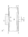
- FIGURE 2 depicts a reverse reach-through APD 200 that may be an integral part of a unit cell 160 depicted in FIGURE 1 , in accordance with certain embodiments of the present disclosure.
- APD 200 may include substrate 202, a highly-doped front-side p-type region 204, a contact 206, field oxides 208, overglass 210, bump 212, highly-doped back-side p-type region 214, highly-doped back-side n-type region 216, and antireflective coating 218.
- Substrate 202 may comprise any substantially intrinsic semiconductor substrate (e.g., undoped or lightly-doped intrinsic semiconductor), including without limitation silicon, germanium, silicon carbide, gallium antimonide, gallium arsenide, gallium nitride, gallium phosphide, indium antimonide, indium arsenide, indium nitride, indium phosphide, or other suitable semiconductor material.
- substrate 202 may be a lightly p-type doped ( ⁇ ) semiconductor (e.g., silicon doped with boron or other acceptor atom).
- ⁇ lightly p-type doped
- substrate 202 it may have a thickness of between approximately 10 ⁇ m and approximately 40 ⁇ m.
- substrate 202 may have a resitivity of approximately 10 k ⁇ -cm or greater.
- Highly-doped front-side p-type region 204 may be formed in or on substrate 202 via implantation, deposition, epitaxy, or any other suitable fabrication technique.
- highly-doped front-side p-type region 204 may be formed by implanting acceptor atoms (e.g., implanting boron atoms into a silicon substrate) on the front-side surface of substrate 202.
- highly-doped front-side p-type region 204 may be formed by epitaxy.
- substrate 202 comprises silicon
- highly-doped front-side p-type region 204 may be implanted to a depth of approximately 0.5 ⁇ m.
- highly-doped front-side p-type region 204 may have a p-type dopant concentration between approximately 5x10 18 cm -3 and approximately 1x10 19 cm -3 .
- highly-doped front-side p-type region 204 may define a pixel area of a detection device (e.g., detection device 120).
- Contact 206 may be coupled to highly-doped front-side p-type region 204 and may include a generally conductive material (e.g., aluminum, silver, copper, gold, or other suitable metal) to electrically couple highly-doped front-side p-type region 204 to bump 212 and/or other electrical and/or electronic circuitry external to APD 200.
- Contact 206 may be formed on substrate 202 via deposition or any other suitable fabrication technique. For example, contact 206 may be formed by depositing aluminum upon highly-doped front-side p-type region 204.
- Field oxides 208 may be formed on the front-side surface of substrate 202 in order to provide surface passivation of substrate 202.
- Field oxides 208 may be formed in any suitable manner.
- field oxides 208 may be formed by growing silicon dioxide on the substrate.
- Overglass 210 may be formed over field oxides 208 in order to environmentally protect the surface of substrate 202.
- Overglass 210 may be formed in any suitable manner.
- silicon dioxide overglass may be formed by plasma oxidation or silicon nitride (Si 2 N 3 ) overglass may be formed by plasma enhanced chemical vapor deposition.
- Bump 212 may be coupled to contact 206 and may include a generally conductive material (e.g., indium or other suitable metal) to electrically couple contact 206 to other electrical and/or electronic circuitry external to APD 200.
- Bump 212 may be formed on substrate 202 via any suitable fabrication technique.
- bump 212 may be formed by electrochemical plating, vacuum deposition of indium, Direct Bond Interconnect, or other suitable fabrication technique.
- Highly-doped back-side p-type region 214 may be formed in or on substrate 202 via implantation, deposition, epitaxy, or any other suitable fabrication technique.
- highly-doped back-side p-type region 214 may be formed by implanting acceptor atoms (e.g., implanting boron into a silicon substrate) on the back-side surface of substrate 202 to create a highly-doped p-type layer.
- highly-doped back-side p-type region 214 may be formed by epitaxy.
- highly-doped back-side p-type region 214 may have a thickness of approximately 0.5 ⁇ m to approximately 3.0 ⁇ m at a peak implant depth of between approximately 1.0 ⁇ m and approximately 2.0 ⁇ m. In embodiments in which substrate 202 comprises silicon, highly-doped back-side p-type region 214 may have a p-type dopant concentration between approximately 8x10 16 cm -3 and approximately 2x10 17 cm -3 .
- Highly-doped back-side n-type region 216 may be formed in or on substrate 202 via implantation, deposition, epitaxy, or any other suitable fabrication technique.
- highly-doped back-side n-type region 216 may be formed by implanting donor atoms (e.g., implanting arsenic or phosphorous into a silicon substrate) on the back-side surface of substrate 202 to create a highly-doped n-type layer.
- donor atoms e.g., implanting arsenic or phosphorous into a silicon substrate
- highly-doped back-side n-type region 216 may have a thickness of approximately 0.1 ⁇ m at an implant depth of approximately 0.1 ⁇ m.
- substrate 202 may be annealed (e.g., via laser or thermal annealing) to activate the implanted dopants (e.g., dopants implanted to create highly-doped back-side p-type region 214 and highly-doped back-side n-type region 216).
- highly-doped back-side n-type region 216 may have a n-type dopant concentration between approximately 5x10 19 cm -3 and approximately 1x10 20 cm -3 .
- Highly-doped back-side n-type region 216 may be electrically coupled to a contact, and such contact may further be coupled to electric and/or electronic circuitry external to APD 200.
- Antireflective coating 218 may be formed on the back-side of substrate 202 and to reduce the reflection of light incident upon APD 200, thus improving the efficiency of the APD 200 as less light is lost via reflection.
- antireflective coating 218 may comprise magnesium fluoride or any other suitable material (e.g., multi-layer materials).
- Antireflective coating 218 may be formed on substrate 202 using physical vapor deposition or any other suitable fabrication technique.
- antireflective coating 218 may have a thickness of approximately 0.16 ⁇ m.
- each APD 200 in an array may have a common substrate 202, a common highly-doped back-side p-type region 214, a common highly-doped back-side n-type region 216, and a common antireflective coating 218.
- each individual APD 200 may have its own highly-doped front-side p-type region 204, contact 206, and bump 212 defining a pixel in the array.
- APD 200 includes a p-n junction formed by highly-doped back-side p-type region 214 and highly-doped back-side n-type region 216.
- a reverse bias may be applied to the p-n junction (e.g., a negative electric potential applied to highly-doped back-side n-type region 216 referenced to contact 206 and/or bump 212).
- Such reverse bias may create an electric field strength profile within APD 200 similar to that depicted in FIGURE 3 .
- an avalanche region of a relatively high field strength may be formed proximate to the p-n junction, such that free electrons present in the avalanche region may be accelerated by the electric field present in the avalanche region such that the free electrons may strike other atoms in the avalanche region, in turn creating more free electrons through impact ionization.
- the reverse bias may also create a depletion region across the undoped or lightly doped portion of substrate 202 in which free carriers (e.g., electrons and holes) may be accelerated to produce an electrical current.
- a photon of light 220 impinging on the back-side of APD 200 may excite an electron, thereby creating a mobile electron and a positively charged electron hole in the avalanche region, which may in turn create more mobile electrons and holes through impact ionization.
- Such electrons and holes may be swept by the built-in field of the depletion and avalanche regions (e.g., electrons toward highly-doped back-side n-type region 216 and holes toward the contact 206) producing a photocurrent proportional to the intensity of impinging light 220.
- FIGURE 4 depicts another reverse reach-through APD 400 that may be an integral part of a unit cell 160 depicted in FIGURE 1 , in accordance with certain embodiments of the present disclosure.
- APD 400 may include substrate 402, a highly-doped front-side n-type region 404, a contact 406, field oxides 408, overglass 410, bump 412, highly-doped back-side n-type region 414, highly-doped back-side p-type region 416, and antireflective coating 418.
- APD 400 may be similar to APD 200 except that highly-doped front-side p-type region 204 is replaced by highly-doped front-side n-type region 404, highly-doped back-side p-type region 214 is replaced by highly-doped back-side n-type region 414, highly-doped back-side n-type region 216 is replaced by highly-doped back-side p-type region 416, and substrate 202 is replaced with substrate 402.
- Substrate 402 may comprise any substantially intrinsic semiconductor substrate (e.g. undoped or lightly-doped semiconductor), including without limitation silicon, germanium, silicon carbide, gallium antimonide, gallium arsenide, gallium nitride, gallium phosphide, indium antimonide, indium arsenide, indium nitride, indium phosphide, or other suitable semiconductor material.
- substrate 202 may be a lightly n-type doped (v) semiconductor (e.g., silicon doped with arsenic, phosphorous, or other acceptor atom).
- substrate 402 may have a thickness of between approximately 10 ⁇ m and approximately 40 ⁇ m. In embodiments in which substrate 402 comprises silicon, substrate 402 may have a resitivity of approximately 10 k ⁇ -cm or greater.
- Highly-doped front-side n-type region 404 may be formed in or on substrate 402 via implantation, deposition, epitaxy, or any other suitable fabrication technique.
- highly-doped front-side n-type region 404 may be formed by implanting donor atoms (e.g., implanting arsenic and/or phosphorous into a silicon substrate) on the front-side surface of substrate 402.
- highly-doped front-side n-type region 404 may be formed by epitaxy.
- substrate 402 comprises silicon
- highly-doped front-side n-type region 404 may be implanted to a depth of approximately 0.5 ⁇ m.
- highly-doped front-side n-type region 404 may have a n-type dopant concentration between approximately 5x10 18 cm -3 and approximately 1x10 19 cm -3 .
- highly-doped front-side n-type region 404 may define a pixel area of a detection device (e.g., detection device 120).
- Contact 406 may be coupled to highly-doped front-side n-type region 404 and may include a generally conductive material (e.g., aluminum, silver, copper, gold, or other suitable metal) to electrically couple highly-doped front-side n-type region 404 to bump 412 and/or other electrical and/or electronic circuitry external to APD 400.
- Contact 406 may be formed on substrate 402 via deposition or any other suitable fabrication technique. For example, contact 406 may be formed by depositing aluminum upon substrate 402.
- Field oxides 408 may be formed on the front-side surface of substrate 402 in order to provide surface passivation of substrate 402. Field oxides 408 may be formed in any suitable manner. For example, in embodiments in which substrate 402 comprises silicon, field oxides 408 may be formed by growing silicon dioxide on the substrate.
- Overglass 410 may be formed over field oxides 408 in order to environmentally protect the surface of substrate 402.
- Overglass 410 may be formed in any suitable manner.
- silicon dioxide overglass may be formed by plasma oxidation or silicon nitride (Si 2 N 3 ) overglass may be formed by plasma enhanced chemical vapor deposition.
- Bump 412 may be coupled to contact 406 and may include a generally conductive material (e.g., indium or other suitable metal) to electrically couple contact 406 to other electrical and/or electronic circuitry external to APD 400.
- Bump 412 may be formed on substrate 402 via any suitable fabrication technique.
- bump 412 may be formed by electrochemical plating, vacuum deposition of indium, Direct Bond Interconnect, or any other suitable fabrication technique.
- Highly-doped back-side n-type region 414 may be formed in or on substrate 402 via implantation, deposition, epitaxy, or any other suitable fabrication technique.
- highly-doped back-side n-type region 414 may be formed by implanting donor atoms (e.g., implanting arsenic or phosphorous into a silicon substrate) on the back-side surface of substrate 402 to create a highly-doped n-type layer.
- highly-doped back-side n-type region 414 may be formed by epitaxy.
- highly-doped back-side n-type region 414 may have a thickness of approximately 1.0 ⁇ m at a peak implant depth of between approximately 1.0 ⁇ m and approximately 2.0 ⁇ m. In embodiments in which substrate 402 comprises silicon, highly-doped back-side n-type region 414 may have a n-type dopant concentration between approximately 8x10 16 cm -3 and approximately 2x10 17 cm -3 .
- Highly-doped back-side p-type region 416 may be formed in or on substrate 402 via implantation, deposition, epitaxy, or any other suitable fabrication technique.
- highly-doped back-side p-type region 416 may be formed by implanting acceptor atoms (e.g., implanting boron into a silicon substrate) on the back-side surface of substrate 402 to create a highly-doped p-type layer.
- substrate 402 comprises silicon
- highly-doped back-side p-type region 416 may have a thickness of approximately 0.1 ⁇ m at an implant depth of approximately 0.1 ⁇ m.
- substrate 402 may be annealed (e.g., via laser or thermal annealing) to activate the implanted dopants (e.g., dopants implanted to create highly-doped back-side n-type region 414 and highly-doped back-side p-type region 416).
- highly-doped back-side p-type region 416 may have a p-type dopant concentration between approximately 5x10 19 cm -3 and approximately 1x10 20 cm -3 .
- Highly-doped back-side p-type region 416 may be electrically coupled to a contact and such contact may further be coupled to electric and/or electronic circuitry external to APD 400.
- Antireflective coating 418 may be formed on the back-side of substrate 402 and to reduce the reflection of light incident upon APD 400, thus improving the efficiency of the APD 400 as less light is lost via reflection.
- Antireflective coating 418 may comprise magnesium fluoride or any other suitable material (e..g, multi-layer materials).
- Antireflective coating 418 may be formed on substrate 402 using physical vapor deposition or any other suitable fabrication technique. In embodiments in which substrate 402 comprises silicon, antireflective coating 418 may have a thickness of approximately 0.16 ⁇ m.
- each APD 400 in an array may have a common substrate 402, a common highly-doped back-side n-type region 414, a common highly-doped back-side p-type region 416, and a common antireflective coating 418.
- each individual APD 400 may have its own highly-doped front-side n-type region 404, contact 406, and bump 412 defining a pixel in the array.
- APD 400 includes a p-n junction formed by highly-doped back-side n-type region 414 and highly-doped back-side p-type region 416.
- a reverse bias may be applied to the p-n junction (e.g., a positive electric potential applied to contact 206 and/or bump 212 referenced to highly-doped back-side p-type region 416).
- Such reverse bias may create an electric field strength profile within APD 400 similar to that depicted in FIGURE 3 .
- an avalanche region of a relatively high field strength may be formed proximate to the p-n junction, such that free electrons present in the avalanche region may be accelerated by the electric field present in the avalanche region such that the free electrons may strike other atoms in the avalanche region, in turn creating more free electrons through impact ionization.
- the reverse bias may also create a depletion region across the undoped or lightly doped portion of substrate 402 in which free carriers (e.g., electrons and holes) may be accelerated to produce an electrical current.
- a photon of light 420 impinging on the back-side of APD 400 may excite an electron, thereby creating a mobile electron and a positively charged electron hole in the avalanche region, which may in turn create more mobile electrons and holes through impact ionization.
- Such electrons and holes may be swept by the built-in field of the depletion and avalanche regions (e.g., holes toward highly-doped back-side p-type region 216 and electrons toward the contact 206) producing a photocurrent proportional to the intensity of impinging light 220.
- APDs such as APD 200 and APD 400 may have a higher signal-to-noise ratio (SNR) as compared with conventional APDs.
- SNR signal-to-noise ratio
- noise generated in a depletion region is often multiplied through impact ionization in the avalanche region.
- a reverse reach-through APD such as the APDs depicted in FIGURES 2 and 4
- optically-generated free electrons may be multiplied whereas noise multiplication may be reduced as compared to traditional approaches.
- the buried p-n junctions may render the APD less sensitive to surface conditions, resulting in lower surface dark current compared and stronger radiation hardening characteristics as compared with traditional approaches.
- reverse reach-through APDs such as the APDs depicted in FIGURES 2 and 4 may be relatively simple to fabricate, as the structure of the APDs depicted in FIGURES 2 and 4 are similar to those of a traditional PiN diode with either an additional highly-doped p-type region (e.g., highly-doped back-side p-type region 214 in FIGURE 2 ) or an additional highly-doped n-type region (highly-doped back-side n-type region 414 in FIGURE 4 ).
- an additional highly-doped p-type region e.g., highly-doped back-side p-type region 214 in FIGURE 2
- an additional highly-doped n-type region highly-doped back-side n-type region 414 in FIGURE 4 .
Landscapes
- Light Receiving Elements (AREA)
- Solid State Image Pick-Up Elements (AREA)
Abstract
A reverse reach-through avalanche photodiode may include a first region (202) comprising substantially intrinsic semiconductor material, the first region (202) having a first side and a second side opposite to the first side. The photodiode may also include a second region (204) comprising highly-doped p-type semiconductor material formed proximate to the first side of the first region (202). The photodiode may additionally include a third region (216) comprising highly-doped n-type semiconductor material formed proximate to the second side of the first region (202). The photodiode may further include a fourth region (214) comprising one of: (i) highly-doped p-type semiconductor formed between the first region (202) and the third region (216), or (ii) highly-doped n-type semiconductor formed between the first region (202) and the second region (204).
Description
- This disclosure relates in general to photodetection and more particularly to a photodetection system and method utilizing one or more avalanche photodiodes.
- Photodetector circuits (e.g., focal plane arrays) are utilized in various devices to sense incident light in the visible and non-visible spectra. Photodetector circuits typically consist of an array of photodiodes that generate a charge, current, or voltage in proportion to the light intensity received at the location of each detector pixel.
- Conventionally, such photodiodes include PN diodes, PiN diodes and avalanche photodiodes (APDs). APDs are photodetectors that may be regarded as photon-multipliers. By applying a reverse bias voltage to an APD (typically 10 volts or more in silicon), APDs show an internal current gain effect (a gain of approximately 10 or more) due to phenomenon known as impact ionization or the avalanche effect. Because of this large gain, APDs have found to be particularly useful in high-sensitivity photodetection. However, conventional APDs are often not suitable for "back-side" illuminated devices which may be required for certain photodetection applications, in particular large-format focal plane arrays. In addition, conventional APDs are known to multiply signal (i.e., incident light) as well as noise, which is often undesirable in high-sensitivity applications.
- According to one embodiment, a photodiode may include a first region comprising substantially intrinsic semiconductor material, the region having a first side and a second side opposite to the first side. The photodiode may also include a second region comprising highly-doped p-type semiconductor material formed proximate to the first side of the first region. The photodiode may additionally include a third region comprising highly-doped n-type semiconductor material formed proximate to the second side of the first region. The photodiode may further include a fourth region comprising (i) highly-doped p-type semiconductor formed between the first region and the third region, or (ii) highly-doped n-type semiconductor formed between the first region and the second region.
- Technical advantages of certain embodiments may include providing a photodiode with higher signal-to-noise ratio as compared with conventional photodiodes.
- Other technical advantages will be readily apparent to one skilled in the art from the following figures, descriptions, and claims. Moreover, while specific advantages have been enumerated above, various embodiments may include all, some, or none of the enumerated advantages.
- For a more complete understanding of the present disclosure and its advantages, reference is now made to the following description, taken in conjunction with the accompanying drawings, in which:
-
FIGURE 1 is a simplified schematic diagram illustrating a photodetection system, in accordance with embodiments of the present disclosure; -
FIGURE 2 depicts a reverse reach-through APD that may be an integral part of a photodetector depicted inFIGURE 1 , in accordance with certain embodiments of the present disclosure; -
FIGURE 3 depicts an electric field strength profile of the APD depicted inFIGURE 2 in a reverse-biased configuration, in accordance with certain embodiments of the present disclosure; and -
FIGURE 4 depicts another reverse reach-through APD that may be an integral part of a photodetector depicted inFIGURE 1 , in accordance with certain embodiments of the present disclosure. - Embodiments of the present disclosure and its advantages are best understood by referring to
FIGURES 1 through 4 of the drawings, like numerals being used for like and corresponding parts of the various drawings. -
FIGURE 1 is a block diagram illustratingphotodetection system 100, in accordance with embodiments of the present disclosure. For example,photodetection system 100 may be a digital camera, video camera, or any other photographic device, image capturing device, and/or high-speed photon counting device.Photodetection system 100 may includedetection device 120 andsignal processing unit 140.Detection device 120 may be a focal plane array (FPA), active pixel sensor (APS) or any other suitable light sensing device that can capture photons.Detection device 120 may include, for example, one or more diodes, complimentary metal-oxide semiconductors (CMOSs), charge-coupled devices (CCDs), or any other suitable photovoltaic detectors or transducers.Signal processing unit 140 may be a combination of hardware, software, or firmware that is operable to receive signal information fromdetection device 120 and convert the signal information into electronic data. -
Detection device 120 may include an array ofunit cells 160.Unit cells 160 may accumulate charge or produce a current and/or voltage proportional to the light intensity of light incident upon the unit cell and may correspond to a pixel in a captured electronic signal. The accumulated charge or the produced current and/or voltage may be used byprocessing unit 140 for processing of the incident light (e.g., to create a signal representative of the incident light). In certain embodiments, one or more ofunit cells 160 may include a reverse reach-through APD, such as the reverse reach-through APDs depicted inFIGURES 2 and4 . -
FIGURE 2 depicts a reverse reach-throughAPD 200 that may be an integral part of aunit cell 160 depicted inFIGURE 1 , in accordance with certain embodiments of the present disclosure. As shown inFIGURE 2 , APD 200 may includesubstrate 202, a highly-doped front-side p-type region 204, acontact 206,field oxides 208,overglass 210,bump 212, highly-doped back-side p-type region 214, highly-doped back-side n-type region 216, andantireflective coating 218. -
Substrate 202 may comprise any substantially intrinsic semiconductor substrate (e.g., undoped or lightly-doped intrinsic semiconductor), including without limitation silicon, germanium, silicon carbide, gallium antimonide, gallium arsenide, gallium nitride, gallium phosphide, indium antimonide, indium arsenide, indium nitride, indium phosphide, or other suitable semiconductor material. In some embodiments,substrate 202 may be a lightly p-type doped (π) semiconductor (e.g., silicon doped with boron or other acceptor atom). In embodiments in whichsubstrate 202 comprises silicon, it may have a thickness of between approximately 10 µm and approximately 40 µm. In embodiments in whichsubstrate 202 comprises silicon,substrate 202 may have a resitivity of approximately 10 kΩ-cm or greater. - Highly-doped front-side p-
type region 204 may be formed in or onsubstrate 202 via implantation, deposition, epitaxy, or any other suitable fabrication technique. For example, highly-doped front-side p-type region 204 may be formed by implanting acceptor atoms (e.g., implanting boron atoms into a silicon substrate) on the front-side surface ofsubstrate 202. In other embodiments, highly-doped front-side p-type region 204 may be formed by epitaxy. In embodiments in whichsubstrate 202 comprises silicon, highly-doped front-side p-type region 204 may be implanted to a depth of approximately 0.5 µm. In embodiments in whichsubstrate 202 comprises silicon, highly-doped front-side p-type region 204 may have a p-type dopant concentration between approximately 5x1018 cm-3 and approximately 1x1019 cm-3. In some embodiments, highly-doped front-side p-type region 204 may define a pixel area of a detection device (e.g., detection device 120). - Contact 206 may be coupled to highly-doped front-side p-
type region 204 and may include a generally conductive material (e.g., aluminum, silver, copper, gold, or other suitable metal) to electrically couple highly-doped front-side p-type region 204 tobump 212 and/or other electrical and/or electronic circuitry external toAPD 200. Contact 206 may be formed onsubstrate 202 via deposition or any other suitable fabrication technique. For example,contact 206 may be formed by depositing aluminum upon highly-doped front-side p-type region 204. -
Field oxides 208 may be formed on the front-side surface ofsubstrate 202 in order to provide surface passivation ofsubstrate 202.Field oxides 208 may be formed in any suitable manner. For example, in embodiments in whichsubstrate 202 comprises silicon,field oxides 208 may be formed by growing silicon dioxide on the substrate. -
Overglass 210 may be formed overfield oxides 208 in order to environmentally protect the surface ofsubstrate 202.Overglass 210 may be formed in any suitable manner. For example, in embodiments in whichsubstrate 202 comprises silicon, silicon dioxide overglass may be formed by plasma oxidation or silicon nitride (Si2N3) overglass may be formed by plasma enhanced chemical vapor deposition. -
Bump 212 may be coupled to contact 206 and may include a generally conductive material (e.g., indium or other suitable metal) to electrically couplecontact 206 to other electrical and/or electronic circuitry external toAPD 200.Bump 212 may be formed onsubstrate 202 via any suitable fabrication technique. For example,bump 212 may be formed by electrochemical plating, vacuum deposition of indium, Direct Bond Interconnect, or other suitable fabrication technique. - Highly-doped back-side p-
type region 214 may be formed in or onsubstrate 202 via implantation, deposition, epitaxy, or any other suitable fabrication technique. For example, highly-doped back-side p-type region 214 may be formed by implanting acceptor atoms (e.g., implanting boron into a silicon substrate) on the back-side surface ofsubstrate 202 to create a highly-doped p-type layer. In other embodiments, highly-doped back-side p-type region 214 may be formed by epitaxy. In embodiments in whichsubstrate 202 comprises silicon, highly-doped back-side p-type region 214 may have a thickness of approximately 0.5 µm to approximately 3.0 µm at a peak implant depth of between approximately 1.0 µm and approximately 2.0 µm. In embodiments in whichsubstrate 202 comprises silicon, highly-doped back-side p-type region 214 may have a p-type dopant concentration between approximately 8x1016 cm-3 and approximately 2x1017 cm-3. - Highly-doped back-side n-
type region 216 may be formed in or onsubstrate 202 via implantation, deposition, epitaxy, or any other suitable fabrication technique. For example, highly-doped back-side n-type region 216 may be formed by implanting donor atoms (e.g., implanting arsenic or phosphorous into a silicon substrate) on the back-side surface ofsubstrate 202 to create a highly-doped n-type layer. In embodiments in whichsubstrate 202 comprises silicon, highly-doped back-side n-type region 216 may have a thickness of approximately 0.1 µm at an implant depth of approximately 0.1 µm. After implantation,substrate 202 may be annealed (e.g., via laser or thermal annealing) to activate the implanted dopants (e.g., dopants implanted to create highly-doped back-side p-type region 214 and highly-doped back-side n-type region 216). In some embodiments, highly-doped back-side n-type region 216 may have a n-type dopant concentration between approximately 5x1019 cm-3 and approximately 1x1020 cm-3. Highly-doped back-side n-type region 216 may be electrically coupled to a contact, and such contact may further be coupled to electric and/or electronic circuitry external toAPD 200. -
Antireflective coating 218 may be formed on the back-side ofsubstrate 202 and to reduce the reflection of light incident uponAPD 200, thus improving the efficiency of theAPD 200 as less light is lost via reflection. In embodiments in whichsubstrate 202 comprises silicon,antireflective coating 218 may comprise magnesium fluoride or any other suitable material (e.g., multi-layer materials).Antireflective coating 218 may be formed onsubstrate 202 using physical vapor deposition or any other suitable fabrication technique. In embodiments in whichsubstrate 202 comprises silicon,antireflective coating 218 may have a thickness of approximately 0.16 µm. - In applications in which
numerous APDs 200 are used in an array of unit cells (e.g., detection device 120), certain portions of one or more APDs 200 may be common to each other. For example, eachAPD 200 in an array may have acommon substrate 202, a common highly-doped back-side p-type region 214, a common highly-doped back-side n-type region 216, and a commonantireflective coating 218. In such an array, eachindividual APD 200 may have its own highly-doped front-side p-type region 204, contact 206, and bump 212 defining a pixel in the array. - In the configuration shown in
FIGURE 2 ,APD 200 includes a p-n junction formed by highly-doped back-side p-type region 214 and highly-doped back-side n-type region 216. In operation, a reverse bias may be applied to the p-n junction (e.g., a negative electric potential applied to highly-doped back-side n-type region 216 referenced to contact 206 and/or bump 212). Such reverse bias may create an electric field strength profile withinAPD 200 similar to that depicted inFIGURE 3 . If the applied reverse bias voltage is large enough (e.g., approximately 30 volts or greater in embodiments in whichsubstrate 202 comprises silicon) an avalanche region of a relatively high field strength may be formed proximate to the p-n junction, such that free electrons present in the avalanche region may be accelerated by the electric field present in the avalanche region such that the free electrons may strike other atoms in the avalanche region, in turn creating more free electrons through impact ionization. The reverse bias may also create a depletion region across the undoped or lightly doped portion ofsubstrate 202 in which free carriers (e.g., electrons and holes) may be accelerated to produce an electrical current. - Accordingly, a photon of light 220 impinging on the back-side of
APD 200 may excite an electron, thereby creating a mobile electron and a positively charged electron hole in the avalanche region, which may in turn create more mobile electrons and holes through impact ionization. Such electrons and holes may be swept by the built-in field of the depletion and avalanche regions (e.g., electrons toward highly-doped back-side n-type region 216 and holes toward the contact 206) producing a photocurrent proportional to the intensity of impinginglight 220. -
FIGURE 4 depicts another reverse reach-throughAPD 400 that may be an integral part of aunit cell 160 depicted inFIGURE 1 , in accordance with certain embodiments of the present disclosure. As shown inFIGURE 4 ,APD 400 may includesubstrate 402, a highly-doped front-side n-type region 404, acontact 406,field oxides 408,overglass 410,bump 412, highly-doped back-side n-type region 414, highly-doped back-side p-type region 416, andantireflective coating 418.APD 400 may be similar toAPD 200 except that highly-doped front-side p-type region 204 is replaced by highly-doped front-side n-type region 404, highly-doped back-side p-type region 214 is replaced by highly-doped back-side n-type region 414, highly-doped back-side n-type region 216 is replaced by highly-doped back-side p-type region 416, andsubstrate 202 is replaced withsubstrate 402. -
Substrate 402 may comprise any substantially intrinsic semiconductor substrate (e.g. undoped or lightly-doped semiconductor), including without limitation silicon, germanium, silicon carbide, gallium antimonide, gallium arsenide, gallium nitride, gallium phosphide, indium antimonide, indium arsenide, indium nitride, indium phosphide, or other suitable semiconductor material. In some embodiments,substrate 202 may be a lightly n-type doped (v) semiconductor (e.g., silicon doped with arsenic, phosphorous, or other acceptor atom). In the same or alternative embodiments,substrate 402 may have a thickness of between approximately 10 µm and approximately 40 µm. In embodiments in whichsubstrate 402 comprises silicon,substrate 402 may have a resitivity of approximately 10 kΩ-cm or greater. - Highly-doped front-side n-
type region 404 may be formed in or onsubstrate 402 via implantation, deposition, epitaxy, or any other suitable fabrication technique. For example, highly-doped front-side n-type region 404 may be formed by implanting donor atoms (e.g., implanting arsenic and/or phosphorous into a silicon substrate) on the front-side surface ofsubstrate 402. In other embodiments, highly-doped front-side n-type region 404 may be formed by epitaxy. In embodiments in whichsubstrate 402 comprises silicon, highly-doped front-side n-type region 404 may be implanted to a depth of approximately 0.5 µm. In embodiments in whichsubstrate 402 comprises silicon, highly-doped front-side n-type region 404 may have a n-type dopant concentration between approximately 5x1018 cm-3 and approximately 1x1019 cm-3. In some embodiments, highly-doped front-side n-type region 404 may define a pixel area of a detection device (e.g., detection device 120). - Contact 406 may be coupled to highly-doped front-side n-
type region 404 and may include a generally conductive material (e.g., aluminum, silver, copper, gold, or other suitable metal) to electrically couple highly-doped front-side n-type region 404 to bump 412 and/or other electrical and/or electronic circuitry external toAPD 400. Contact 406 may be formed onsubstrate 402 via deposition or any other suitable fabrication technique. For example, contact 406 may be formed by depositing aluminum uponsubstrate 402. -
Field oxides 408 may be formed on the front-side surface ofsubstrate 402 in order to provide surface passivation ofsubstrate 402.Field oxides 408 may be formed in any suitable manner. For example, in embodiments in whichsubstrate 402 comprises silicon,field oxides 408 may be formed by growing silicon dioxide on the substrate. -
Overglass 410 may be formed overfield oxides 408 in order to environmentally protect the surface ofsubstrate 402.Overglass 410 may be formed in any suitable manner. For example, in embodiments in whichsubstrate 402 comprises silicon, silicon dioxide overglass may be formed by plasma oxidation or silicon nitride (Si2N3) overglass may be formed by plasma enhanced chemical vapor deposition. - Bump 412 may be coupled to contact 406 and may include a generally conductive material (e.g., indium or other suitable metal) to
electrically couple contact 406 to other electrical and/or electronic circuitry external toAPD 400. Bump 412 may be formed onsubstrate 402 via any suitable fabrication technique. For example, bump 412 may be formed by electrochemical plating, vacuum deposition of indium, Direct Bond Interconnect, or any other suitable fabrication technique. - Highly-doped back-side n-
type region 414 may be formed in or onsubstrate 402 via implantation, deposition, epitaxy, or any other suitable fabrication technique. For example, highly-doped back-side n-type region 414 may be formed by implanting donor atoms (e.g., implanting arsenic or phosphorous into a silicon substrate) on the back-side surface ofsubstrate 402 to create a highly-doped n-type layer. In other embodiments, highly-doped back-side n-type region 414 may be formed by epitaxy. In embodiments in whichsubstrate 402 comprises silicon, highly-doped back-side n-type region 414 may have a thickness of approximately 1.0 µm at a peak implant depth of between approximately 1.0 µm and approximately 2.0 µm. In embodiments in whichsubstrate 402 comprises silicon, highly-doped back-side n-type region 414 may have a n-type dopant concentration between approximately 8x1016 cm-3 and approximately 2x1017 cm-3. - Highly-doped back-side p-
type region 416 may be formed in or onsubstrate 402 via implantation, deposition, epitaxy, or any other suitable fabrication technique. For example, highly-doped back-side p-type region 416 may be formed by implanting acceptor atoms (e.g., implanting boron into a silicon substrate) on the back-side surface ofsubstrate 402 to create a highly-doped p-type layer. In embodiments in whichsubstrate 402 comprises silicon, highly-doped back-side p-type region 416 may have a thickness of approximately 0.1 µm at an implant depth of approximately 0.1 µm. After implantation,substrate 402 may be annealed (e.g., via laser or thermal annealing) to activate the implanted dopants (e.g., dopants implanted to create highly-doped back-side n-type region 414 and highly-doped back-side p-type region 416). In embodiments in whichsubstrate 402 comprises silicon, highly-doped back-side p-type region 416 may have a p-type dopant concentration between approximately 5x1019 cm-3 and approximately 1x1020 cm-3. Highly-doped back-side p-type region 416 may be electrically coupled to a contact and such contact may further be coupled to electric and/or electronic circuitry external toAPD 400. -
Antireflective coating 418 may be formed on the back-side ofsubstrate 402 and to reduce the reflection of light incident uponAPD 400, thus improving the efficiency of theAPD 400 as less light is lost via reflection.Antireflective coating 418 may comprise magnesium fluoride or any other suitable material (e..g, multi-layer materials).Antireflective coating 418 may be formed onsubstrate 402 using physical vapor deposition or any other suitable fabrication technique. In embodiments in whichsubstrate 402 comprises silicon,antireflective coating 418 may have a thickness of approximately 0.16 µm. - In applications in which
numerous APDs 400 are used in an array of unit cells (e.g., detection device 120), certain portions of one or more APDs 400 may be common to each other. For example, eachAPD 400 in an array may have acommon substrate 402, a common highly-doped back-side n-type region 414, a common highly-doped back-side p-type region 416, and a commonantireflective coating 418. In such an array, eachindividual APD 400 may have its own highly-doped front-side n-type region 404, contact 406, and bump 412 defining a pixel in the array. - In the configuration shown in
FIGURE 4 ,APD 400 includes a p-n junction formed by highly-doped back-side n-type region 414 and highly-doped back-side p-type region 416. In operation, a reverse bias may be applied to the p-n junction (e.g., a positive electric potential applied to contact 206 and/or bump 212 referenced to highly-doped back-side p-type region 416). Such reverse bias may create an electric field strength profile withinAPD 400 similar to that depicted inFIGURE 3 . If the applied reverse bias voltage is large enough (e.g., approximately 40 volts or greater in embodiments in whichsubstrate 402 comprises silicon) an avalanche region of a relatively high field strength may be formed proximate to the p-n junction, such that free electrons present in the avalanche region may be accelerated by the electric field present in the avalanche region such that the free electrons may strike other atoms in the avalanche region, in turn creating more free electrons through impact ionization. The reverse bias may also create a depletion region across the undoped or lightly doped portion ofsubstrate 402 in which free carriers (e.g., electrons and holes) may be accelerated to produce an electrical current. - Accordingly, a photon of light 420 impinging on the back-side of
APD 400 may excite an electron, thereby creating a mobile electron and a positively charged electron hole in the avalanche region, which may in turn create more mobile electrons and holes through impact ionization. Such electrons and holes may be swept by the built-in field of the depletion and avalanche regions (e.g., holes toward highly-doped back-side p-type region 216 and electrons toward the contact 206) producing a photocurrent proportional to the intensity of impinginglight 220. - An advantage of APDs such as
APD 200 andAPD 400 is that such APDs may have a higher signal-to-noise ratio (SNR) as compared with conventional APDs. In traditional reach-through APDs, noise generated in a depletion region is often multiplied through impact ionization in the avalanche region. However, in a reverse reach-through APD such as the APDs depicted inFIGURES 2 and4 , optically-generated free electrons may be multiplied whereas noise multiplication may be reduced as compared to traditional approaches. In addition, the buried p-n junctions may render the APD less sensitive to surface conditions, resulting in lower surface dark current compared and stronger radiation hardening characteristics as compared with traditional approaches. - In addition, reverse reach-through APDs such as the APDs depicted in
FIGURES 2 and4 may be relatively simple to fabricate, as the structure of the APDs depicted inFIGURES 2 and4 are similar to those of a traditional PiN diode with either an additional highly-doped p-type region (e.g., highly-doped back-side p-type region 214 inFIGURE 2 ) or an additional highly-doped n-type region (highly-doped back-side n-type region 414 inFIGURE 4 ). - Although the embodiments in the disclosure have been described in detail, numerous changes, substitutions, variations, alterations, and modifications may be ascertained by those skilled in the art. Additionally or alternatively, while the disclosure may be described predominantly in reference to visible detectors, the embodiments disclosed herein may be utilized with many types of detectors including, but not limited to, visible, infrared, ultraviolet, x-ray, or other radiation detectors. It is intended that the present disclosure encompass all such changes, substitutions, variations, alterations and modifications as falling within the spirit and scope of the appended claims.
- It will be appreciated that optional features of embodiments of the invention can be used together in any number and in any combination. This includes, but is not limited to, using the features of dependent claims in any number, and in any combination.
Claims (16)
- A photodiode (200) comprising:a first region (202) comprising substantially intrinsic semiconductor material, the first region (202) having a first side and a second side opposite to the first side;a second region (204) comprising highly-doped p-type semiconductor material formed proximate to the first side of the first region (202);a third region (216) comprising highly-doped n-type semiconductor material formed proximate to the second side of the first region (202); anda fourth region (214) comprising one of: (i) highly-doped p-type semiconductor formed between the first region (202) and the third region (216), or (ii) highly-doped n-type semiconductor formed between the first region (202) and the second region (204).
- The photodiode (200) of Claim 1, wherein the first region (202), the second region (204), the third region (216), and the fourth region (214) are formed on the same semiconductor substrate.
- The photodiode (200) of Claim 1, wherein at least one of the second region (204) and the fourth region (214) is formed by one of: (i) implantation of acceptor atoms into the semiconductor substrate and (ii) acceptor-doped epitaxial growth.
- The photodiode (200) of Claim 1, wherein at least one of the third region (216) and the fourth region (214) is formed by one of: (i) implantation of donor atoms into the semiconductor substrate and (ii) donor-doped epitaxial growth.
- The photodiode (200) of Claim 1, wherein:the fourth region (214) comprises highly-doped p-type semiconductor formed between the first region (202) and the third region (216); andthe first region (202) comprises lightly-doped p-type semiconductor material.
- The photodiode (200) of Claim 1, wherein:the fourth region (214) comprises highly-doped n-type semiconductor formed between the first region (202) and the second region (204); andthe first region (202) comprises lightly-doped n-type semiconductor material.
- The photodiode (200) of Claim 1, wherein one of the second region (204) and the third region (216) defines a pixel area of the photodiode (200).
- A system (100) for photodetection comprising:at least one photodiode (200) according to any of Claims 1-7 and operable to generate an electric signal in proportion to an intensity of light incident on the at least one photodiode (200); anda processing unit (140) communicatively coupled to the at least one photodiode (200).
- The system (100) of Claim 8, wherein the electric signal is one of a voltage, a current and an electric charge.
- The system (100) of Claim 8, comprising a focal plane array including the at least one photodiode (200).
- A method for photodetection comprising:forming a first region (202) comprising substantially intrinsic semiconductor material, the first region (202) having a first side and a second side opposite to the first side;forming a second region (204) comprising highly-doped p-type semiconductor material formed proximate to the first side of the first region (202);forming a third region (216) comprising highly-doped n-type semiconductor material formed proximate to the second side of the first region (202); andforming a fourth region (214) comprising one of: (i) highly-doped p-type semiconductor formed between the first region (202) and the third region (216), or (ii) highly-doped n-type semiconductor formed between the first region (202) and the second region (204).
- The method of Claim 11, wherein the first region (202), the second region (204), the third region (216), and the fourth region (214) are formed on the same semiconductor substrate.
- The method of Claim 11, wherein at least one of the second region (204) and the fourth region (214) is formed by one of: (i) implantation of acceptor atoms into the semiconductor substrate and (ii) acceptor-doped epitaxial growth.
- The method of Claim 11, wherein at least one of the third region (216) and the fourth region (214) is formed by one of: (i) implantation of donor atoms into the semiconductor substrate and (ii) donor-doped epitaxial growth.
- The method of Claim 11, wherein:the fourth region (214) comprises highly-doped p-type semiconductor formed between the first region (202) and the third region (216); andthe first region (202) comprises lightly-doped p-type semiconductor material.
- The method of Claim 11, wherein:the fourth region (214) comprises highly-doped n-type semiconductor formed between the first region (202) and the second region (204); andthe first region (202) comprises lightly-doped n-type semiconductor material.
Applications Claiming Priority (1)
| Application Number | Priority Date | Filing Date | Title |
|---|---|---|---|
| US12/492,903 US20100327387A1 (en) | 2009-06-26 | 2009-06-26 | Avalanche Photodiode |
Publications (1)
| Publication Number | Publication Date |
|---|---|
| EP2267795A2 true EP2267795A2 (en) | 2010-12-29 |
Family
ID=42985493
Family Applications (1)
| Application Number | Title | Priority Date | Filing Date |
|---|---|---|---|
| EP10166949A Withdrawn EP2267795A2 (en) | 2009-06-26 | 2010-06-22 | Avalanche photodiode |
Country Status (4)
| Country | Link |
|---|---|
| US (1) | US20100327387A1 (en) |
| EP (1) | EP2267795A2 (en) |
| JP (1) | JP2011009749A (en) |
| TW (1) | TW201110390A (en) |
Cited By (1)
| Publication number | Priority date | Publication date | Assignee | Title |
|---|---|---|---|---|
| CN108761911A (en) * | 2018-05-29 | 2018-11-06 | Oppo(重庆)智能科技有限公司 | Display module and electronic equipment |
Families Citing this family (40)
| Publication number | Priority date | Publication date | Assignee | Title |
|---|---|---|---|---|
| US9289132B2 (en) | 2008-10-07 | 2016-03-22 | Mc10, Inc. | Catheter balloon having stretchable integrated circuitry and sensor array |
| US8886334B2 (en) | 2008-10-07 | 2014-11-11 | Mc10, Inc. | Systems, methods, and devices using stretchable or flexible electronics for medical applications |
| US8389862B2 (en) | 2008-10-07 | 2013-03-05 | Mc10, Inc. | Extremely stretchable electronics |
| US9123614B2 (en) | 2008-10-07 | 2015-09-01 | Mc10, Inc. | Methods and applications of non-planar imaging arrays |
| US9545216B2 (en) | 2011-08-05 | 2017-01-17 | Mc10, Inc. | Catheter balloon methods and apparatus employing sensing elements |
| US8097926B2 (en) | 2008-10-07 | 2012-01-17 | Mc10, Inc. | Systems, methods, and devices having stretchable integrated circuitry for sensing and delivering therapy |
| WO2011041727A1 (en) | 2009-10-01 | 2011-04-07 | Mc10, Inc. | Protective cases with integrated electronics |
| WO2012166686A2 (en) | 2011-05-27 | 2012-12-06 | Mc10, Inc. | Electronic, optical and/or mechanical apparatus and systems and methods for fabricating same |
| US9757050B2 (en) | 2011-08-05 | 2017-09-12 | Mc10, Inc. | Catheter balloon employing force sensing elements |
| CN103946680A (en) * | 2011-09-28 | 2014-07-23 | Mc10股份有限公司 | Electronics for detection of a property of a surface |
| US9226402B2 (en) | 2012-06-11 | 2015-12-29 | Mc10, Inc. | Strain isolation structures for stretchable electronics |
| US9295842B2 (en) | 2012-07-05 | 2016-03-29 | Mc10, Inc. | Catheter or guidewire device including flow sensing and use thereof |
| JP2015521894A (en) | 2012-07-05 | 2015-08-03 | エムシー10 インコーポレイテッドMc10,Inc. | Catheter device including flow sensing |
| US9171794B2 (en) | 2012-10-09 | 2015-10-27 | Mc10, Inc. | Embedding thin chips in polymer |
| CN105008949A (en) | 2012-10-09 | 2015-10-28 | Mc10股份有限公司 | Conformal electronics integrated with apparel |
| CN104885222B (en) | 2012-12-18 | 2018-03-02 | 松下知识产权经营株式会社 | Light detecter for semiconductor |
| US9706647B2 (en) | 2013-05-14 | 2017-07-11 | Mc10, Inc. | Conformal electronics including nested serpentine interconnects |
| US9224768B2 (en) * | 2013-08-05 | 2015-12-29 | Raytheon Company | Pin diode structure having surface charge suppression |
| KR20160040670A (en) | 2013-08-05 | 2016-04-14 | 엠씨10, 인크 | Flexible temperature sensor including conformable electronics |
| US10467926B2 (en) | 2013-10-07 | 2019-11-05 | Mc10, Inc. | Conformal sensor systems for sensing and analysis |
| JP6711750B2 (en) | 2013-11-22 | 2020-06-17 | エムシー10 インコーポレイテッドMc10,Inc. | Conformal sensor system for detection and analysis of cardiac activity |
| WO2015103580A2 (en) | 2014-01-06 | 2015-07-09 | Mc10, Inc. | Encapsulated conformal electronic systems and devices, and methods of making and using the same |
| KR20160129007A (en) | 2014-03-04 | 2016-11-08 | 엠씨10, 인크 | Multi-part flexible encapsulation housing for electronic devices |
| US9899330B2 (en) | 2014-10-03 | 2018-02-20 | Mc10, Inc. | Flexible electronic circuits with embedded integrated circuit die |
| US10297572B2 (en) | 2014-10-06 | 2019-05-21 | Mc10, Inc. | Discrete flexible interconnects for modules of integrated circuits |
| USD781270S1 (en) | 2014-10-15 | 2017-03-14 | Mc10, Inc. | Electronic device having antenna |
| EP3258837A4 (en) | 2015-02-20 | 2018-10-10 | Mc10, Inc. | Automated detection and configuration of wearable devices based on on-body status, location, and/or orientation |
| US10398343B2 (en) | 2015-03-02 | 2019-09-03 | Mc10, Inc. | Perspiration sensor |
| US10653332B2 (en) | 2015-07-17 | 2020-05-19 | Mc10, Inc. | Conductive stiffener, method of making a conductive stiffener, and conductive adhesive and encapsulation layers |
| US10709384B2 (en) | 2015-08-19 | 2020-07-14 | Mc10, Inc. | Wearable heat flux devices and methods of use |
| CN108290070A (en) | 2015-10-01 | 2018-07-17 | Mc10股份有限公司 | Method and system for interacting with a virtual environment |
| WO2017062508A1 (en) | 2015-10-05 | 2017-04-13 | Mc10, Inc. | Method and System for Neuromodulation and Stimulation |
| EP3420732B8 (en) | 2016-02-22 | 2020-12-30 | Medidata Solutions, Inc. | System, devices, and method for on-body data and power transmission |
| CN108781313B (en) | 2016-02-22 | 2022-04-08 | 美谛达解决方案公司 | Systems, devices, and methods for coupled hubs and sensor nodes for on-body acquisition of sensor information |
| CN109310340A (en) | 2016-04-19 | 2019-02-05 | Mc10股份有限公司 | Method and system for measuring sweat |
| US10447347B2 (en) | 2016-08-12 | 2019-10-15 | Mc10, Inc. | Wireless charger and high speed data off-loader |
| US10312391B2 (en) * | 2016-10-04 | 2019-06-04 | Omnivision Technologies, Inc. | Apparatus and method for single-photon avalanche-photodiode detectors with reduced dark count rate |
| US11538948B2 (en) * | 2019-06-26 | 2022-12-27 | University Of South Carolina | Quantum dot photovoltaic junctions |
| WO2022004172A1 (en) * | 2020-06-29 | 2022-01-06 | ソニーセミコンダクタソリューションズ株式会社 | Imaging device and electronic apparatus |
| KR102711235B1 (en) * | 2022-06-24 | 2024-09-27 | 주식회사 트루픽셀 | SINGLE PHOTON DETECTION ELEMENT, ELECTRONIC DEVICE, AND LiDAR DEVICE |
Family Cites Families (2)
| Publication number | Priority date | Publication date | Assignee | Title |
|---|---|---|---|---|
| US5164809A (en) * | 1989-04-21 | 1992-11-17 | The Regents Of The University Of Calif. | Amorphous silicon radiation detectors |
| GB9710301D0 (en) * | 1997-05-21 | 1997-07-16 | Philips Electronics Nv | Image sensor and its manufacture |
-
2009
- 2009-06-26 US US12/492,903 patent/US20100327387A1/en not_active Abandoned
-
2010
- 2010-06-18 TW TW099119894A patent/TW201110390A/en unknown
- 2010-06-22 EP EP10166949A patent/EP2267795A2/en not_active Withdrawn
- 2010-06-25 JP JP2010144976A patent/JP2011009749A/en active Pending
Non-Patent Citations (1)
| Title |
|---|
| None |
Cited By (1)
| Publication number | Priority date | Publication date | Assignee | Title |
|---|---|---|---|---|
| CN108761911A (en) * | 2018-05-29 | 2018-11-06 | Oppo(重庆)智能科技有限公司 | Display module and electronic equipment |
Also Published As
| Publication number | Publication date |
|---|---|
| US20100327387A1 (en) | 2010-12-30 |
| TW201110390A (en) | 2011-03-16 |
| JP2011009749A (en) | 2011-01-13 |
Similar Documents
| Publication | Publication Date | Title |
|---|---|---|
| US20100327387A1 (en) | Avalanche Photodiode | |
| US11888003B2 (en) | Photodetector | |
| US10056416B2 (en) | Majority current assisted radiation detector device | |
| US9881963B1 (en) | Horizontal avalanche photodiode | |
| US9178100B2 (en) | Single photon avalanche diode for CMOS circuits | |
| EP2474034B1 (en) | Low energy portable low-light camera with wavelength cutoff | |
| US8946617B2 (en) | Photodiode having a p-n junction with varying expansion of the space charge zone due to application of a variable voltage | |
| US10367111B2 (en) | APD focal plane arrays with backside vias | |
| US12078728B2 (en) | High dynamic range single photon avalanche detector array on silicon with circuitry for light detection and ranging | |
| US8212327B2 (en) | High fill-factor laser-treated semiconductor device on bulk material with single side contact scheme | |
| CN116457630A (en) | Light receiving element, photodetector, and ranging system | |
| US11817518B2 (en) | Multi-junction pico-avalanche detector | |
| CN108987421A (en) | A kind of back-illuminated single-photon avalanche diode imaging sensor | |
| CN119277830A (en) | A low noise semiconductor photodetector | |
| EP4428933A1 (en) | Single photon detection element, electronic device and lidar device | |
| WO2022254797A1 (en) | Photodetection element, method for making photo detection element, and electronic device | |
| WO2021213674A1 (en) | Photodiode and method for operating a photodiode | |
| US20260020365A1 (en) | Photodiode with deep trench isolation structures and intermediate doped regions | |
| WO2011092601A2 (en) | Bio-inspired nanostructures for implementing vertical pn-junctions | |
| Goto et al. | Crystalline selenium layer stacked image sensors with pixel-parallel A/D converters toward photon counting | |
| WO2023069916A1 (en) | Buried photodetector with hetero structure as a gate | |
| Stern et al. | High quantum efficiency, back-illuminated, crystallographically etched, silicon-on-sapphire avalanche photodiode with very wide dynamic range, for manufacturable high resolution imaging arrays | |
| US20240030360A1 (en) | Photodiode device with high responsivity | |
| CN119290175A (en) | A semiconductor single-photon detector with wide spectrum and high detection efficiency | |
| WO2009111748A2 (en) | High fill-factor laser-treated semiconductor device on bulk material with single side contact scheme |
Legal Events
| Date | Code | Title | Description |
|---|---|---|---|
| PUAI | Public reference made under article 153(3) epc to a published international application that has entered the european phase |
Free format text: ORIGINAL CODE: 0009012 |
|
| AK | Designated contracting states |
Kind code of ref document: A2 Designated state(s): AL AT BE BG CH CY CZ DE DK EE ES FI FR GB GR HR HU IE IS IT LI LT LU LV MC MK MT NL NO PL PT RO SE SI SK SM TR |
|
| AX | Request for extension of the european patent |
Extension state: BA ME RS |
|
| STAA | Information on the status of an ep patent application or granted ep patent |
Free format text: STATUS: THE APPLICATION IS DEEMED TO BE WITHDRAWN |
|
| 18D | Application deemed to be withdrawn |
Effective date: 20140103 |