EP2267596B1 - Prozessorkern zur Verarbeitung von Befehlen verschiedener Formate - Google Patents
Prozessorkern zur Verarbeitung von Befehlen verschiedener Formate Download PDFInfo
- Publication number
- EP2267596B1 EP2267596B1 EP10183715.1A EP10183715A EP2267596B1 EP 2267596 B1 EP2267596 B1 EP 2267596B1 EP 10183715 A EP10183715 A EP 10183715A EP 2267596 B1 EP2267596 B1 EP 2267596B1
- Authority
- EP
- European Patent Office
- Prior art keywords
- instructions
- digital signal
- signal processor
- microcontroller
- operations
- Prior art date
- Legal status (The legal status is an assumption and is not a legal conclusion. Google has not performed a legal analysis and makes no representation as to the accuracy of the status listed.)
- Expired - Lifetime
Links
- 238000000034 method Methods 0.000 claims description 15
- 230000004044 response Effects 0.000 claims description 15
- 230000009977 dual effect Effects 0.000 claims description 9
- 239000000203 mixture Substances 0.000 claims description 2
- 238000010586 diagram Methods 0.000 description 14
- 101100059544 Arabidopsis thaliana CDC5 gene Proteins 0.000 description 8
- 101150115300 MAC1 gene Proteins 0.000 description 8
- 101100244969 Arabidopsis thaliana PRL1 gene Proteins 0.000 description 6
- 102100039558 Galectin-3 Human genes 0.000 description 6
- 101100454448 Homo sapiens LGALS3 gene Proteins 0.000 description 6
- 101150051246 MAC2 gene Proteins 0.000 description 6
- 230000006870 function Effects 0.000 description 6
- 230000002093 peripheral effect Effects 0.000 description 6
- 238000003491 array Methods 0.000 description 3
- 101100496858 Mus musculus Colec12 gene Proteins 0.000 description 1
- 230000000903 blocking effect Effects 0.000 description 1
- 238000004364 calculation method Methods 0.000 description 1
- 230000021615 conjugation Effects 0.000 description 1
- 230000008030 elimination Effects 0.000 description 1
- 238000003379 elimination reaction Methods 0.000 description 1
- 230000010354 integration Effects 0.000 description 1
- 238000012986 modification Methods 0.000 description 1
- 230000004048 modification Effects 0.000 description 1
- 230000008520 organization Effects 0.000 description 1
- 230000003252 repetitive effect Effects 0.000 description 1
- 238000010187 selection method Methods 0.000 description 1
Images


Classifications
-
- G—PHYSICS
- G06—COMPUTING; CALCULATING OR COUNTING
- G06F—ELECTRIC DIGITAL DATA PROCESSING
- G06F9/00—Arrangements for program control, e.g. control units
- G06F9/06—Arrangements for program control, e.g. control units using stored programs, i.e. using an internal store of processing equipment to receive or retain programs
- G06F9/30—Arrangements for executing machine instructions, e.g. instruction decode
- G06F9/30145—Instruction analysis, e.g. decoding, instruction word fields
-
- G—PHYSICS
- G06—COMPUTING; CALCULATING OR COUNTING
- G06F—ELECTRIC DIGITAL DATA PROCESSING
- G06F9/00—Arrangements for program control, e.g. control units
- G06F9/06—Arrangements for program control, e.g. control units using stored programs, i.e. using an internal store of processing equipment to receive or retain programs
- G06F9/30—Arrangements for executing machine instructions, e.g. instruction decode
- G06F9/30003—Arrangements for executing specific machine instructions
- G06F9/30007—Arrangements for executing specific machine instructions to perform operations on data operands
- G06F9/3001—Arithmetic instructions
-
- G—PHYSICS
- G06—COMPUTING; CALCULATING OR COUNTING
- G06F—ELECTRIC DIGITAL DATA PROCESSING
- G06F9/00—Arrangements for program control, e.g. control units
- G06F9/06—Arrangements for program control, e.g. control units using stored programs, i.e. using an internal store of processing equipment to receive or retain programs
- G06F9/30—Arrangements for executing machine instructions, e.g. instruction decode
- G06F9/30003—Arrangements for executing specific machine instructions
- G06F9/30007—Arrangements for executing specific machine instructions to perform operations on data operands
- G06F9/30036—Instructions to perform operations on packed data, e.g. vector, tile or matrix operations
-
- G—PHYSICS
- G06—COMPUTING; CALCULATING OR COUNTING
- G06F—ELECTRIC DIGITAL DATA PROCESSING
- G06F9/00—Arrangements for program control, e.g. control units
- G06F9/06—Arrangements for program control, e.g. control units using stored programs, i.e. using an internal store of processing equipment to receive or retain programs
- G06F9/30—Arrangements for executing machine instructions, e.g. instruction decode
- G06F9/30145—Instruction analysis, e.g. decoding, instruction word fields
- G06F9/30149—Instruction analysis, e.g. decoding, instruction word fields of variable length instructions
-
- G—PHYSICS
- G06—COMPUTING; CALCULATING OR COUNTING
- G06F—ELECTRIC DIGITAL DATA PROCESSING
- G06F9/00—Arrangements for program control, e.g. control units
- G06F9/06—Arrangements for program control, e.g. control units using stored programs, i.e. using an internal store of processing equipment to receive or retain programs
- G06F9/30—Arrangements for executing machine instructions, e.g. instruction decode
- G06F9/38—Concurrent instruction execution, e.g. pipeline or look ahead
- G06F9/3867—Concurrent instruction execution, e.g. pipeline or look ahead using instruction pipelines
- G06F9/3873—Variable length pipelines, e.g. elastic pipeline
-
- G—PHYSICS
- G06—COMPUTING; CALCULATING OR COUNTING
- G06F—ELECTRIC DIGITAL DATA PROCESSING
- G06F9/00—Arrangements for program control, e.g. control units
- G06F9/06—Arrangements for program control, e.g. control units using stored programs, i.e. using an internal store of processing equipment to receive or retain programs
- G06F9/30—Arrangements for executing machine instructions, e.g. instruction decode
- G06F9/38—Concurrent instruction execution, e.g. pipeline or look ahead
- G06F9/3867—Concurrent instruction execution, e.g. pipeline or look ahead using instruction pipelines
- G06F9/3875—Pipelining a single stage, e.g. superpipelining
-
- G—PHYSICS
- G06—COMPUTING; CALCULATING OR COUNTING
- G06F—ELECTRIC DIGITAL DATA PROCESSING
- G06F9/00—Arrangements for program control, e.g. control units
- G06F9/06—Arrangements for program control, e.g. control units using stored programs, i.e. using an internal store of processing equipment to receive or retain programs
- G06F9/30—Arrangements for executing machine instructions, e.g. instruction decode
- G06F9/38—Concurrent instruction execution, e.g. pipeline or look ahead
- G06F9/3885—Concurrent instruction execution, e.g. pipeline or look ahead using a plurality of independent parallel functional units
- G06F9/3887—Concurrent instruction execution, e.g. pipeline or look ahead using a plurality of independent parallel functional units controlled by a single instruction for multiple data lanes [SIMD]
-
- G—PHYSICS
- G06—COMPUTING; CALCULATING OR COUNTING
- G06F—ELECTRIC DIGITAL DATA PROCESSING
- G06F9/00—Arrangements for program control, e.g. control units
- G06F9/06—Arrangements for program control, e.g. control units using stored programs, i.e. using an internal store of processing equipment to receive or retain programs
- G06F9/30—Arrangements for executing machine instructions, e.g. instruction decode
- G06F9/38—Concurrent instruction execution, e.g. pipeline or look ahead
- G06F9/3885—Concurrent instruction execution, e.g. pipeline or look ahead using a plurality of independent parallel functional units
- G06F9/3893—Concurrent instruction execution, e.g. pipeline or look ahead using a plurality of independent parallel functional units controlled in tandem, e.g. multiplier-accumulator
Definitions
- This invention relates to digital signal processors and, more particularly, to digital signal processor computation core architectures that facilitate complex digital signal processing computations.
- a digital signal computer or digital signal processor (DSP) is a special purpose computer that is designed to optimize performance for digital signal processing applications, such as, for example, Fast Fourier transforms, digital filters, image processing and speech recognition.
- Digital signal processor applications are typically characterized by real-time operation, high interrupt rates and intensive numeric computations.
- digital signal processor applications tend to be intensive in memory access operations and to require the input and output of large quantities of data.
- Digital signal processor architectures are typically optimized for performing such computations efficiently.
- Microcontrollers involve the handling of data but typically do not require extensive computation.
- Microcontroller application programs tend to be longer than DSP programs.
- DSP programs In order to limit the memory requirements of microcontroller application programs, it is desirable to provide a high degree of code density in such programs.
- architectures that are optimized for DSP computations typically do not operate efficiently as microcontrollers.
- microcontrollers typically do not perform well as digital signal processors. Nonetheless, a particular application may require both digital signal processor and microcontroller functionality.
- Digital signal processor designs may be optimized with respect to different operating parameters, such as computation speed and power consumption, depending on intended applications. Furthermore, digital signal processors may be designed for 16-bit words, 32-bit words, or other word sizes. A 32-bit architecture that achieves very high operating speed is disclosed in U. S. Patent No. 5,954,811 issued September 21,1999 to Garde .
- Digital signal processors frequently utilize architectures wherein two or more data words are stored in each row of memory, and two or more data words are provided in parallel to the computation unit. Such architectures provide enhanced performance, because several instructions and/or operands may be accessed simultaneously.
- EP 0789297A discloses a data processor comprising a computation core in which a first and second decoder decode operation code for data load and multiply - add operations in parallel.
- An operand access unit then causes 2 n bit data, stored in internal memory, to the transferred also in parallel to a first operation unit and then stored in respect of predetermined registers.
- a first aspect provides a computer core according to claim 1.
- a second aspect provides a method for executing programmed instructions according to claim 5.
- a computation core for executing programmed instructions.
- the computation core comprises an execution block for performing digital signal processor operations in response to digital signal processor instructions and for performing microcontroller operations in response to microcontroller instructions, a register file for storing operands for and results of the digital signal processor operations and the microcontroller operations, and control logic for providing control signals to the execution block and the register file in response to the digital signal processor instructions and the microcontroller instructions for executing the digital signal processor instructions and the microcontroller instructions characterized in that said digital signal processor instructions contain information indicating whether one or more related load or store instructions follow.
- the digital signal processor instructions are configured for high efficiency digital signal computations, and the microcontroller instructions are configured for code storage density.
- the microcontroller instructions have a 16-bit format and the digital signal processor instructions have a 32-bit format.
- the digital signal processor instructions contain information indicating whether one or more related instructions follow.
- the related instructions comprise load instructions.
- a method for executing programmed instructions.
- the method comprises the steps of executing digital signal processor operations in an execution block in response to digital signal processor instructions configured for efficient digital signal computation, and executing microcontroller operations in the execution block in response to microcontroller instructions configured for code storage density.
- An application program having a mixture of digital signal processor instructions and microcontroller instructions is characterized by high code storage density and efficient digital signal computation characterized in that said digital signal processor instructions contain information indicating whether one or more related load or store instructions follow.
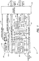
- FIG. 1 A block diagram of an embodiment of a computation core 10 in accordance with the invention is shown in FIG. 1 .
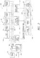
- a block diagram of a digital signal processor 20 incorporating computation core 10 is shown in FIG. 2 .
- digital signal processor 20 is implemented as a monolithic integrated circuit which incorporates computation core 10.
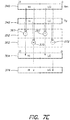
- Computation core 10 includes a computation block 24 and an addressing block 26 coupled through operand buses 30 and result buses 32 to a memory interface 34. Address buses 40 and 42 are coupled between addressing block 26 and memory interface 34. Computation core 10 further includes an instruction sequencer 50 coupled by an instruction address bus 52 and an instruction bus 54 to memory interface 34. Memory interface 34 is connected by memory buses 60 and 62 to a memory 64 ( FIG. 2 ), including memory banks 70, 72, 74 and 76, located external to computation core 10.
- computation block 24 includes a register file 80 and execution units 82 and 84, each of which are connected to operand buses 30 and result buses 32.
- Execution unit 82 (execution unit 0) includes an arithmetic logic unit (ALU) 90, a multiplier 92, an accumulator 94, and a shifter 96.
- Execution unit 84 (execution unit 1) includes an ALU 100, a multiplier 102, and an accumulator 104. The structure and operation of computation block 24 are described in detail below.
- the addressing block 26 includes an address register file 120 and data address generators 124.
- address register file 120 has a capacity of 8 address values.
- the address register file 120 may be used for microcontroller programs that require simple addressing, and may access different word widths (8-bit bytes, 16-bit half words, and 32-bit words).
- the addressing block 26 may include four data address generators (DAGs) 124 for generating address sequences or patterns.
- DAGs data address generators
- Instruction sequencer 50 includes a loop buffer 130, an instruction decoder 132 and sequencer/control logic 134. Instructions are received from memory 64 through one of the memory buses 60 or 62 and are delivered to the instruction sequencer 50 via instruction bus 54. The instructions are temporarily stored in loop buffer 130. The loop buffer 130 is used for implementing repetitive code sequences with no overhead. The instructions are decoded in the instruction decoder 132 and are interpreted by the sequencer/control logic 134 to control operations by the rest of the computation core.
- the integration of computation core 10 into digital signal processor 20 is shown in FIG. 2 .
- Core 10 is connected to the other elements of the digital signal processor 20 through memory buses 60 and 62.
- the digital signal processor 20 may further include a memory bus 150, which is not connected to computation core 10 and an industry standard bus 152, also not connected to computation core 10.
- Standard bus 152 may, for example, be a Peripheral Components Interconnect (PCI) bus and may be connected to memory buses 60, 62 and 150 through a peripheral bus bridge 154.
- PCI Peripheral Components Interconnect
- memory buses 60, 62 and 150 are connected to memory banks 70, 72, 74 and 76, peripheral bus bridge 154, a DMA controller 160 and an external memory bus controller 162.
- the external memory bus controller 162 permits the digital signal processor 20 to be connected to an external memory via an external memory bus 164.
- the standard bus 152 may be connected to a custom peripheral interface 170, a serial port 172, a microcontroller host port 174, an FPGA (field programmable gate array) based peripheral 176, a custom algorithm accelerator 178 and a purchased peripheral interface 180. It will be understood that different elements may be added to or removed from the digital signal processor 20 for different applications.
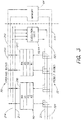
- register file 80 has eight registers and is partitioned into register file banks 200 and 202, each having four registers of 32 bits each.
- register file bank 200 contains registers R0-R3
- register file bank 202 contains registers R4-R7. This arrangement results in low power because each four entry register file bank 200, 202 requires less energy per access than a single eight entry register file.
- Each four entry register file bank 200, 202 requires two read ports and two write ports, while an eight entry register file requires four read ports and four write ports.
- Register file 80 is connected to execution units 82 and 84 and to memory 64 by operand buses 30 and result buses 32.
- Operand buses 30 include operand bus 210, operand bus 212, operand bus 214 and operand bus 216.
- Operand buses 210 and 212 are connected between register file banks 200 and 202 and memory 64 for writing results of computations to memory. In another embodiment, a single operand bus may be used for writing data from register file 80 to memory 64.
- Operand buses 214 and 216 are connected between register file banks 200 and 202 and execution units 82 and 84 for supplying operands to execution units 82 and 84.
- Result buses 32 include result bus 220, result bus 222, result bus 224 and result bus 226.
- Result buses 220 and 222 are connected between memory 64 and register file banks 200 and 202 for reading operands from memory 64.
- Result buses 224 and 226 are connected between execution units 82 and 84 and register file banks 200 and 202 for writing results of computations in register file 80.
- each of operand buses 210, 212, 214 and 216 and each of result buses 220, 222, 224 and 226 is 32 bits wide.
- memory 64 is external to computation core 10.
- the connections to memory 64 are via memory interface 34 and memory buses 60 and 62, as described above in connection with FIGS. 1 and 2 .
- FIG. 3A A block diagram of a second embodiment of register file 80, execution units 82 and 84 and memory 64, and the interconnection between these elements, is shown in FIG. 3A .
- register file 80 has a single register file bank 240 having eight registers, R0-R7, of 32 bits each.
- Register file bank 240 has four read ports and four write ports.
- FIG. 4 A block diagram of execution units 82 and 84 is shown in FIG. 4 .
- a portion of execution unit 82 is shown in more detail in FIG. 4A .
- Execution unit 82 includes a multiplier array 250, an ALU 252, an accumulator 254 and a barrel shifter 256.
- Execution unit 84 includes a multiplier array 260, an ALU 262 and an accumulator 264.
- Each multiplier array 250, 260 receives two 16-bit operands and provides two 32-bit outputs to the respective ALUs 252, 262.
- ALUs 252 and 262 may also receive two 32-bit inputs from operand buses 214 and 216.
- ALUs 252 and 262 are 40-bit ALUs.
- the output of ALU 252 is connected to accumulator 254 and is connected through a result swap mux (multiplexer) 280 to one input of an output select mux 282.
- the output of accumulator 254 is connected to a second input of output select mux 282 and is connected to an input of ALU 252.
- the output of ALU 262 is connected to accumulator 264 and is connected through a result swap mux 284 to an output select mux 286.
- the output of accumulator 264 is connected to a second input of output select mux 286 and to an input of ALU 262.
- the output of output select mux 282 is connected to result bus 226, and the output of output select mux 286 is connected to result bus 224.
- multiplier arrays 250 and 260 and the ALUs 252 and 262 are utilized.
- multiply accumulate (MAC) operations multiplier arrays 250 and 260, ALU's 252 and 262 and accumulators 254 and 264 are utilized.
- add/subtract operations ALUs 252 and 262 are utilized. The appropriate outputs are selected by output select muxes 282 and 286 and are supplied on result buses 226 and 224 to register file 80.
- the operations of the execution units 82 and 84 are described in more detail below.
- FIG. 4 shows only the data paths in the execution units 82 and 84.
- Each element of execution units 82 and 84 receives control signals from the sequencer/control logic 134 ( FIG. 1 ) for controlling operations in accordance with instructions being executed.
- Each of the operand buses 214 and 216 is 32 bits wide and carries two 16-bit operands, designated as a high operand and a low operand.
- the computation block 24 is preferably provided with an arrangement of data selectors which permits the multiplier in each of execution units 82 and 84 to select the high or low operand from each of the operand buses 214 and 216.
- a mux (data selector) 300 selects the high operand or the low operand from operand bus 214 for input to multiplier array 250
- a mux 302 selects the high operand or the low operand from operand bus 216 for input to multiplier array 250.
- a mux 310 selects the high operand or the low operand from operand bus 214 for input to multiplier array 260
- a mux 312 selects the high operand or the low operand from operand bus 216 for input to multiplier array 260.
- the select inputs to muxes 300, 302, 310 and 312 are controlled in response to information contained in instructions as described below. This arrangement for selecting operands provides a high degree of flexibility in performing digital signal computations.
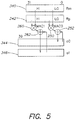
- FIG. 5 A schematic representation of a dual multiply accumulate operation by execution units 82 and 84 is shown in FIG. 5 .
- a 32-bit data element 340 represents the operands supplied from register file 80 on operand bus 214
- a 32-bit data element 342 represents the operands supplied from register file 80 on operand bus 216
- a 40-bit data element 344 represents the contents of accumulator 254, and a 40-bit data element 346 represents the contents of accumulator 264.
- Multiplier array 250 receives the low operands from data elements 340 and 342 and supplies an output to ALU 252.
- ALU 252 adds the output of multiplier array 250 and data element 344 and places the result in accumulator 254 as a new data element 344.
- multiplier array 260 receives the high operands from data elements 340 and 342 and supplies an output to ALU 262.
- ALU 262 adds the output of multiplier array 260 and data element 346 from accumulator 264 and places the result in accumulator 264 as a new data element 346.
- muxes 300 and 302 select the low operands from operand buses 214 and 216 and supply the low operands to multiplier array 250.
- Muxes 310 and 312 select the high operands from operand buses 214 and 216 and supply the high operands to multiplier array 260.
- FIGS. 6A-6D Selection of different operands for computation by execution unit 82 is illustrated in the schematic representations of FIGS. 6A-6D . Like elements in FIGS. 4 , 5 and 6A-6D have the same reference numerals.
- the low operand of data element 340 and the low operand of data element 342 are supplied to multiplier array 250.
- FIG. 6B the high operand of data element 340 and the low operand of data element 342 are supplied to multiplier array 250.
- FIG. 6C the low operand of data element 340 and the high operand of data element 342 are supplied to multiplier array 250.
- FIG. 6A the low operand of data element 340 and the low operand of data element 342 are supplied to multiplier array 250.
- the high operand of data element 340 and the low operand of data element 342 are supplied to multiplier array 250.
- FIG. 6C the low operand of data element 340 and the high operand of data element 342 are supplied to multiplier array 250.
- the high operand of data element 340 and the high operand of data element 342 are supplied to multiplier array 250.
- the data element 340 appears on operand bus 214 ( FIG. 4 )
- the data element 342 appears on operand bus 216.
- the selection of operands for multiplier array 250 is made by muxes 300 and 302, as shown in FIG. 4 .
- muxes 310 and 312 perform operand selection for multiplier array 260.
- the muxes 300, 302, 310 and 312 are controlled by select signals derived from instructions being executed, as described below.
- the operand selection technique is described above in connection with dual multiply accumulate (MAC) units. However, since this technique relates to the data movement and selection aspects of computation, it is generally applicable to data selection for any execution unit that performs any arbitrary arithmetic operation. In addition, although the description relates to selection of one of two 16-bit operands, the operand selection technique can be implemented with operands of any width and with two or more operands. When using the operand selection technique, the programmer selects two pairs of adjacent 16-bit data elements that reside in register file 80.
- the programmer selects a high or low 16-bit operand from a 32-bit data element to serve as one input to one of the MACs.
- the other input to the same MAC is a high or low 16-bit operand selected from the other operand bus.
- the execution units 82 and 84 also execute instructions which specify ALU operations, i.e., operations which involve addition or subtraction and which do not require the multiplier array or the accumulator.
- the ALUs 252 and 262 may be configured for performing various ALU operations. In most cases, only one of the ALU's 252 and 262 is active in performing ALU operations. An exception is shown in FIG. 7E and is described below. ALU operations are described in connection with ALU 252 and execution unit 82. It will be understood that the same ALU operations can be performed by ALU 262 in execution unit 84.
- ALU 252 performs a 32-bit add or subtract and outputs a 32-bit result through result swap mux 280 and output select mux 282 to result bus 226.
- the ALU 252 may be configured for performing two 16-bit addition or subtraction operations, as illustrated in FIGS. 7A-7D .
- 32-bit ALU 252 is configured to function as two 16-bit ALUs 360 and 362 ( FIG. 4A ).
- a 32-bit ALU may be configured as two independent 16-bit ALUs by blocking the carry from bit 15 into bit 16.
- ALU 360 adds the high operands of data elements 340 and 342 and places the 16-bit result in a high result portion of a data element 364.
- ALU 362 adds the low operands of data elements 340 and 342 and places the result in a low result portion of data element 364.
- the 32-bit data element 364 is supplied on result bus 226 to register file 80.
- FIGS. 7A, 7B, 7C and 7D illustrate the fact that 16-bit ALUs 360 and 362 are separately programmable in response to control 1 and control 0 signals ( FIG. 4A ), and may perform the same or different operations.
- FIG. 7A illustrates the case where ALU 360 and ALU 362 both perform add operations.
- FIG. 7B illustrates the case where ALU 360 and ALU 362 both perform subtract operations.
- FIG. 7C illustrates the case where ALU 360 performs an add operation and ALU 362 performs a subtract operation.
- FIG. 7D illustrates the case where ALU 360 performs a subtract operation and ALU 362 performs an add operation.
- the control 1 and control 0 signals are supplied from instruction decoder 132 ( FIG. 1 ) in response to decoding of an instruction being executed.
- ALU operations typically utilize only one of the execution units 82 and 84.
- An exception is described with reference to FIG. 7E .
- the 16-bit ALU 360 subtracts the high operands of data elements 340 and 342 and places the result in the high result portion of data word 364.
- the 16-bit ALU 362 adds the low operands of data elements 340 and 342 and places the result in the low result portion of data element 364.
- This configuration further utilizes 32-bit ALU 262 in execution unit 84 configured as 16-bit ALUs 370 and 372.
- the 16-bit ALU 370 adds the high operands of data elements 340 and 342 and places the result in a high result portion of a data element 374.
- the 16-bit ALU 372 subtracts the low operands of data elements 340 and 342 and places the result in a low result portion of data element 374.
- Data element 374 is supplied on result bus 224 to register file 80.
- execution units 82 and 84 simultaneously perform four 16-bit ALU operations.
- FIGS. 7A-7D illustrate a configuration where 16-bit ALU 360 and 16-bit ALU 362 are separately programmable and the operations performed by ALUs 360 and 362 may be the same or different.
- an ALU instruction includes operation fields which specify the individual operations to be performed by ALUs 360 and 362.
- This individual control feature is generally applicable to any execution units that perform two or more operations simultaneously.
- the multiplier accumulators in execution units 82 and 84 are individually controllable and may perform the same or different operations.
- a multiplier accumulator instruction includes operation fields which individually specify the operations to be performed by execution units 82 and 84.
- the individual control feature can be implemented with execution units of any type or width, and with two or more execution units, or with a single execution unit having two or more computation devices.
- a further feature of execution units 82 and 84 is described with reference to FIGS. 4A and 8 .
- the results generated by 16-bit ALUs 360 and 362 may be reversed, or swapped, with respect to their placement in 32-bit data element 364.
- the output of ALU 360 is supplied to the low result portion of data element 364, and the output of ALU 362 is supplied to the high result portion of data element 364.
- This reversed or swapped configuration is contrasted with the configuration of FIGS. 7A-7D , where the output of ALU 360 is supplied to the high result portion of data element 364 and the output of ALU 362 is supplied to the low result portion of data element 364.
- the reversal or swapping of the outputs of ALUs 360 and 362 is performed by result swap mux 280 ( FIG. 4 ) in response to information contained in an instruction.
- the result swapping operation at the output of ALUs 360 and 362 is useful, for example, to achieve conjugation in complex arithmetic.
- result swap mux 280 may include a mux 380, which is controlled by a swap signal, and a mux 382, which is controlled by an inverted swap signal.
- Each of the muxes 380 and 382 receives the 16-bit results from ALUs 360 and 362.
- the swap signal is not asserted, the output of ALU 360 is supplied to the high result portion of result bus 226, and the output of ALU 362 is supplied to the low result portion of result bus 226.
- the swap signal is asserted, the output of ALU 360 is supplied to the low result portion of result bus 226, and the output of ALU 362 is supplied to the high result portion of result bus 226, thereby swapping the outputs of ALUs 360 and 362.
- output select mux 282 FIG. 4
- FIG. 4 output select mux 282 is omitted for simplicity of illustration.
- the result swapping technique is described above in connection with swapping of ALU outputs. However, since this technique relates to the data movement aspects of computation, it is generally applicable to result swapping for any execution unit that produces two or more results. As described below in connection with FIG. 10 , an ALU instruction includes a field which specifies whether or not the results of the ALU operations are to be swapped. The result swapping technique can be implemented with results of any width and with two or more results.
- a multiplier accumulator instruction 400 has a 32-bit format, with the fields of the instructions as shown in FIG. 9 .
- Operation fields, op0 and op1 each having two bits, indicate the operations to be performed by execution units 82 and 84, respectively.
- the operations include multiply, multiply-add, multiply-subtract and no operation.
- the multiply-add and multiply-subtract operations are MAC operations.
- a P field indicates whether the result is to be written to a single register or written to a register pair.
- Two w fields w1, and w0, indicate whether the result is to be accumulated only or accumulated and written to a register.
- the w1 field applies to execution unit 82, and the w0 field applies to execution unit 84.
- An h00 field indicates whether to select the high operand or the low operand of source 0 (src0) for execution unit 82.
- An h10 field indicates whether to select the high operand or the low operand of source 1 (src1) for execution unit 82.
- An h01 field indicates whether to select the high operand or the low operand of source 0 for execution unit 84.
- An h11 field indicates whether to select the high operand or the low operand of source 1 for execution unit 84.
- the h00 and h10 fields control muxes 300 and 302, respectively, at the inputs to execution unit 82
- the h01 and h11 fields control muxes 310 and 312, respectively, at the inputs to execution unit 84.
- An MM field indicates whether or not execution unit 84 is in mixed mode (signed/unsigned).
- An mmod field indicates fraction or integer operation, signed or unsigned operation, round or truncate operation and scaled or unsealed operation.
- An M field indicates whether or not two load/store instructions follow the instruction.
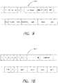
- An example of a DSP type ALU instruction format for controlling execution units 82 and 84 to perform ALU operations is shown in FIG. 10 .
- An ALU instruction 450 has a 32-bit format. As in the case of the multiply accumulate instruction, the M field indicates whether or not two load/store instructions follow the instruction.
- An operation code field, aopcde is used in conjunction with a secondary op code field, aop, to specify a particular arithmetic operation. Examples include single 16-bit ALU operations, single 32-bit ALU operations, dual 16-bit ALU operations and quad 16-bit ALU operations, as well as other arithmetic operations known to those skilled in the art.
- An HL field indicates whether the result of a single ALU operation is to be deposited in the high half or the low half of the destination register.
- An x field indicates whether or not two 16-bit results are to be swapped as they are deposited in the destination register. The value contained in the x field controls the operation of result swap mux 280 ( FIG. 4A ) as described above.
- An s field determines whether saturation is active or inactive.
- the aop field indicates the two operands that are to be added or subtracted, i.e., low and low; low and high; high and low; or high and high.
- the HL field indicates whether the 16-bit result is to be deposited in the high or low half of the destination register.
- the aop field indicates the two operations to be performed by the two 16-bit ALUs, i.e., add/add; add/subtract; subtract/add; or subtract/subtract.
- the aop field controls the individual operations performed by ALUs 360 and 362 (see FIGS. 7A-7D ).
- the aop field controls the operations performed by 16-bit ALUs 360, 362, 370 and 372 ( FIG. 7E ).
- the possible operations are add/add for one execution unit and subtract/subtract for the other execution unit, or add/subtract for one execution unit and subtract/add for the other execution unit, to avoid redundant calculations.
- the aopcde field in instruction 450 may also specify a 32-bit add or subtract operation.
- the instruction formats shown in FIGS. 9 and 10 and described above are DSP instructions. These instructions are characterized by a high degree of flexibility and include optional features to permit efficient digital signal processor computations.
- An example of a microcontroller type instruction format for controlling execution units 82 and 84 to perform arithmetic operations is shown in FIG. 11 .
- An instruction 480 has a length of 16 bits and contains only three fields, a 4-bit operation code field, opc, a 3-bit source field, src, and a 3-bit destination field, dst.
- the input operands are taken from the registers in register file 80 specified by the src and dst fields.
- the result of the computation is placed in the register specified by the dst field, thereby overwriting one of the operands.
- the operation code field, opc may specify add, subtract, multiply, as well as other arithmetic operations known to those skilled in the art. It may be observed that instruction 480 is relatively simple and has only three fields that may be specified by the programmer. However, because instruction 480 has a length of 16 bits, it occupies only half of the memory space that is occupied by the more complex DSP instructions described above
- code density is an important factor in microcontroller applications.
- a typical microcontroller application may have a relatively large number of instructions requiring relatively simple computations and data handling. Because the number of instructions in a microcontroller application may be large, code density is an important factor in minimizing memory requirements.
- DSP applications typically include a relatively small number of instructions which may be executed repetitively in performing DSP computations. Thus, code density is less important than efficient execution in achieving high performance in DSP applications.
- a combined application typically includes a relatively large number of 16-bit microcontroller instructions and a relatively small number of 32-bit DSP instructions, thereby achieving a high degree of code density.
- the relatively small number of DSP instructions can be optimized for the highest performance in executing DSP computations.
- the computation core 10 preferably has a pipeline architecture, as illustrated in FIGS. 12 and 14 .
- the pipeline has eight stages.
- each stage performs a specified function of instruction execution, permitting multiple instructions to be executed simultaneously, with each instruction having a different phase of execution.
- FIG. 12 is a pipeline timing diagram wherein a horizontal row of blocks represents the functions performed by the different stages of the pipeline in executing a single instruction.
- row 500 represents execution of a first instruction
- row 502 represents execution of a second instruction.
- Vertically aligned blocks represent functions that are performed simultaneously by different stages in the pipeline.
- stages 0 and 1 perform instruction fetch (IF) from an instruction cache 510 ( FIG. 14 ).
- Stage 2 performs instruction decoding (ID) in instruction decoder 132.
- Stage 3 performs data address generation (DAG) in DAG 124.
- Stages 4 and 5 perform data memory access (M1 and M2) in memory 64.
- the instruction fetch, instruction decode, data address generation and memory access functions are performed by the control section of computation core 10, including instruction sequencer 50 and addressing block 26 ( FIG. 1 ).
- Stages 4-7 include operations performed by computation block 24.
- Stage 4 performs register file read (RFR) from register file 80.
- Stages 5 and 6 perform multiply accumulate operations (MAC1 and MAC2) in execution units 82 and 84.
- stage 5 the MAC1 operation of stage 5 is executed by multiplier arrays 250 and 260
- the MAC2 operation of stage 6 is executed by ALUs 250 and 262 and accumulators 254 and 264.
- Arithmetic logic and shift operations (EX) of stage 6 are executed by ALUs 252 and 262 or barrel shifter 270.
- the stage 7 operation is a register file write (RFW) from execution units 82 and 84 to register file 80.
- pipeline stages are separated by latches 508 controlled by a system clock, as known in the art.
- the pipeline shown in FIGS. 12 and 14 and described above is optimized for achieving high performance when executing DSP code.
- a feature of the pipeline is that memory access operations (M1 and M2), such as loads and stores, occur early in the pipeline relative to the computation operations (EX, MAC1 and MAC2), thus achieving early memory access.
- FIG. 12 this is illustrated by the arrow from the end of the second memory access stage (M2) in row 500 to the beginning of the first computation stage (MAC1) in row 502.
- the arrow represents a register file bypass operation wherein data loaded from memory is supplied directly to execution units 82 and 84, and register file 80 is bypassed.
- MAC multiply accumulate
- the memory access operations (DAG, M1, and M2) occur relatively early in the pipeline and result in two idle pipeline stages, stages 6 and 7, in the control section of the computation core.
- the computation operations (MAC1 and MAC2) occur relatively late in the pipeline and result in one idle stage (DAG), stage 3, in the computation block 24 of the computation core.
- FIG. 13 A timing diagram for a conventional pipeline is illustrated in FIG. 13 .
- memory access operations DAG, M1, and M2
- DAG, M1, and M2 memory access operations
- MAC1 and MAC2 computation operations
- M1 and M2 memory access operations
- MAC1 and MAC2 computation operations
- stages 4 and 5 a one cycle stall is required between a load instruction and a computation instruction that immediately follows the load instruction.
- the stall may have a significant impact on performance where the sequence of instructions is contained in a loop that is executed multiple times.
- the pipeline structure shown in FIGS. 12 and 14 does not require a stall between a load instruction and a computation instruction.
- the early memory access pipeline structure shown in FIG. 12 has advantages in comparison with the prior art pipeline structure shown in FIG. 13 .
- Load-to-use latencies in processors with execution units that have multiple pipeline stages are eliminated.
- processors with this type of execution unit suffer from load-to-use latencies.
- Elimination of load-to-use latencies results in simpler software that does not require loop unrolling or software pipelining, which are software techniques used to improve performance in processors with load-to-use latencies. Even when these techniques are applied, the performance of a conventional processor may be lower than that of the pipeline structure shown in FIGS. 12 and 14 and described above.
- FIR finite impulse response
- the dual multiply accumulate operations shown in FIGS. 5 and 6A-6D and described above, may be utilized to perform FIR filter computations.
- execution units 82 and 84 may be utilized to perform two multiply accumulate operations simultaneously.
- a conventional implementation of an FIR filter on a DSP with dual execution units would require that a total of four data values be loaded from memory: two input values from x(n) and two filter coefficients from c(n). These data loads are achieved by loading a pair of adjacent data values and a pair of adjacent filter coefficient values.
- a problem with this technique is that for half of the total number of memory accesses, the pairs of data values must come from locations that are not 32-bit aligned in memory. That is, the memory must be able to deliver data elements x(0) and x(1) into a register in an aligned 32-bit access, and must also be able to deliver data elements x(1) and x(2) to a register in a misaligned 32-bit access. Note that either the data elements x(n) or the coefficients c(n) must be accessed as misaligned 32-bit element pairs, but not both. One of these signals may always be accessed as 32-bit aligned pairs, and here it is assumed that coefficients c(n) are accessed as aligned 32-bit pairs. The delivery of misaligned 32-bit element pairs in prior art systems requires two memory accesses and, therefore, is relatively inefficient.
- a novel FIR filter implementation avoids misaligned 32 bit data accesses as follows. Let execution unit 82 (MAC0) compute all of the even indexed outputs and execution unit 84 (MAC1) compute all of the odd indexed outputs. For example, outputs z(0) through z(3) may computed as follows.
- execution units 82 computes z(0) and z(2)
- execution unit 84 computes z(1) and z(3).
- the value z(0) is computed in execution unit 82, and the value z(1) is computed in execution unit 84.
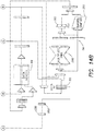
- coefficient pair c(2) and c(3) is loaded into register R1 and a single data sample x(3) is loaded into the high half of register R0, as shown in FIG. 15C .
- the low half of register R0 is not changed.
- FIG. 16 A pseudo-code representation of an algorithm for performing FIR digital filter computations as described above is shown in FIG. 16 .
- the algorithm includes an outer loop and an inner loop.
- the outer loop is executed M/2 times, where M is the number of input data samples in the data set. Since two output values are computed on each pass of the outer loop, M/2 iterations are required.
- a 16-bit data element x(0) is loaded into register RL0, the lower half of register R0, and the inner loop is executed L times, where L is the number of coefficients in the FIR filter.
- the inner loop performs the multiply accumulate operations for values of an index variable k for values of k from 0 to L-1.
- a 16-bit data element x(n+k+1) is loaded into register RH0, the high half of register R0.
- Two 16-bit coefficients c(k+1) and c(k) are loaded into register R1.
- the multiply accumulate value z(n+1) is computed in execution unit 84, and the result is stored in accumulator A1.
- the multiply accumulate value z(n) is computed in execution unit 82, and the result is stored in accumulator A0.
- a 16-bit data element x(n+k+2) is loaded into register RL0, the low half of register R0, and the multiply accumulate values z(n+1) and z(n) are computed.
- the inner loop is executed L times.
Landscapes
- Engineering & Computer Science (AREA)
- Software Systems (AREA)
- Theoretical Computer Science (AREA)
- Physics & Mathematics (AREA)
- General Physics & Mathematics (AREA)
- General Engineering & Computer Science (AREA)
- Mathematical Optimization (AREA)
- Mathematical Analysis (AREA)
- Computational Mathematics (AREA)
- Pure & Applied Mathematics (AREA)
- Mathematical Physics (AREA)
- Advance Control (AREA)
- Executing Machine-Instructions (AREA)
- Complex Calculations (AREA)
- Error Detection And Correction (AREA)
- Filters That Use Time-Delay Elements (AREA)
- Image Processing (AREA)
Claims (5)
- Rechenkern (10) zum Ausführen von programmierten Anweisungen, umfassend:einen Ausführungsblock (82, 84) zum Ausführen von digitalen Signalprozessoroperationen als Reaktion auf digitale Signalprozessoranweisungen und zum Durchführen von Mikrocontrolleroperationen als Reaktion auf Mikrocontrolleranweisungen, wobei die digitalen Signalprozessoranweisungen ein längeres Format als die Mikrocontrolleranweisungen aufweisen, so dass die digitalen Signalprozessoranweisungen für eine effizientere digitale Signalberechnung formatiert sind und die Mikrocontrolleranweisungen für eine höhere Codespeicherdichte als die digitalen Signalprozessoranweisungen formatiert sind;eine Registerdatei (80) zum Speichern von Operanden für die digitalen Signalprozessoroperationen und die Mikrocontrolleroperationen und Ergebnissen von diesen; undeine Steuerlogik (50) zum Bereitstellen von Steuersignalen für den Ausführungsblock und die Registerdatei als Reaktion auf die digitalen Signalprozessoranweisungen und die Mikrocontrolleranweisungen zum Ausführen der digitalen Signalprozessoranweisungen und der Mikrocontrolleranweisungen, dadurch gekennzeichnet, dass die digitalen Signalprozessoranweisungen Informationen enthalten, die angeben, ob eine oder mehrere Lade- oder Speicheranweisungen folgen.
- Rechenkern (10) nach Anspruch 1, wobei die Mikrocontrolleranweisungen ein 16-Bit-Format aufweisen und wobei die digitalen Signalprozessoranweisungen ein 32-Bit-Format aufweisen.
- Rechenkern (10) nach Anspruch 1, wobei der Ausführungsblock (82, 84) duale Ausführungseinheiten umfasst.
- Rechenkern (10) nach Anspruch 3, wobei der Ausführungsblock (82) eine erste Ausführungseinheit einschließlich einer Multipliziersammeleinheit (102, 104), einer arithmetischen Logikeinheit (100) und eines Schaltteils (96) und eine zweite Ausführungseinheit (84) einschließlich einer Multipliziersammeleinheit (92, 94) und einer arithmetischen Logikeinheit (90) umfasst.
- Verfahren zum Ausführen von programmierten Anweisungen, das folgende Schritte umfasst:Ausführen von digitalen Signalprozessoroperationen in einem Ausführungsblock (82, 84) als Reaktion auf digitale Signalprozessoranweisungen; undAusführen von Mikrocontrolleroperationen in dem Ausführungsblock als Reaktion auf Mikrocontrolleranweisungen, wobei die digitalen Signalprozessoranweisungen ein längeres Format als die Mikrocontrolleranweisungen aufweisen, so dass die digitalen Signalprozessoranweisungen für eine effizientere digitale Signalberechnung formatiert sind und die Mikrocontrolleranweisungen für eine höhere Codespeicherdichte als die digitalen Signalprozessoranweisungen formatiert sind, wobei ein Anwendungsprogramm eine Mischung von digitalen Signalprozessoranweisungen und Mikrocontrolleranweisungen aufweist, dadurch gekennzeichnet, dass die digitalen Signalprozessoranweisungen Informationen enthalten, die angeben, ob eine oder mehrere Lade- oder Speicheranweisungen folgen.
Applications Claiming Priority (3)
| Application Number | Priority Date | Filing Date | Title |
|---|---|---|---|
| US13376699P | 1999-05-12 | 1999-05-12 | |
| EP00930720A EP1188112A2 (de) | 1999-05-12 | 2000-05-12 | Berechnungskern eines digitalen signalprozessors |
| PCT/US2000/013232 WO2000068783A2 (en) | 1999-05-12 | 2000-05-12 | Digital signal processor computation core |
Related Parent Applications (2)
| Application Number | Title | Priority Date | Filing Date |
|---|---|---|---|
| EP00930720.8 Division | 2000-05-12 | ||
| EP00930720A Division EP1188112A2 (de) | 1999-05-12 | 2000-05-12 | Berechnungskern eines digitalen signalprozessors |
Publications (3)
| Publication Number | Publication Date |
|---|---|
| EP2267596A2 EP2267596A2 (de) | 2010-12-29 |
| EP2267596A3 EP2267596A3 (de) | 2012-01-04 |
| EP2267596B1 true EP2267596B1 (de) | 2018-08-15 |
Family
ID=22460216
Family Applications (4)
| Application Number | Title | Priority Date | Filing Date |
|---|---|---|---|
| EP10184831A Withdrawn EP2267597A3 (de) | 1999-05-12 | 2000-05-12 | Digitalen Signalprozessor mit Pipeline-Struktur |
| EP10184733A Withdrawn EP2267896A3 (de) | 1999-05-12 | 2000-05-12 | Berechnungskern eines digitalen Signalprozessors |
| EP10183715.1A Expired - Lifetime EP2267596B1 (de) | 1999-05-12 | 2000-05-12 | Prozessorkern zur Verarbeitung von Befehlen verschiedener Formate |
| EP00930720A Withdrawn EP1188112A2 (de) | 1999-05-12 | 2000-05-12 | Berechnungskern eines digitalen signalprozessors |
Family Applications Before (2)
| Application Number | Title | Priority Date | Filing Date |
|---|---|---|---|
| EP10184831A Withdrawn EP2267597A3 (de) | 1999-05-12 | 2000-05-12 | Digitalen Signalprozessor mit Pipeline-Struktur |
| EP10184733A Withdrawn EP2267896A3 (de) | 1999-05-12 | 2000-05-12 | Berechnungskern eines digitalen Signalprozessors |
Family Applications After (1)
| Application Number | Title | Priority Date | Filing Date |
|---|---|---|---|
| EP00930720A Withdrawn EP1188112A2 (de) | 1999-05-12 | 2000-05-12 | Berechnungskern eines digitalen signalprozessors |
Country Status (3)
| Country | Link |
|---|---|
| EP (4) | EP2267597A3 (de) |
| JP (1) | JP2002544587A (de) |
| WO (1) | WO2000068783A2 (de) |
Families Citing this family (11)
| Publication number | Priority date | Publication date | Assignee | Title |
|---|---|---|---|---|
| WO2002010914A1 (en) * | 2000-07-28 | 2002-02-07 | Delvalley Limited | A method of processing data |
| US7174543B2 (en) | 2001-08-29 | 2007-02-06 | Analog Devices, Inc. | High-speed program tracing |
| JP4502662B2 (ja) * | 2004-02-20 | 2010-07-14 | アルテラ コーポレイション | 乗算器−累算器ブロックモード分割 |
| EP1849095B1 (de) * | 2005-02-07 | 2013-01-02 | Richter, Thomas | Vorrichtung zur verarbeitung massiver paralleldaten mit geringer latenz |
| CN100559905C (zh) * | 2005-07-20 | 2009-11-11 | 大唐移动通信设备有限公司 | 基带芯片 |
| US7555514B2 (en) | 2006-02-13 | 2009-06-30 | Atmel Corportation | Packed add-subtract operation in a microprocessor |
| JP5481793B2 (ja) * | 2008-03-21 | 2014-04-23 | 富士通株式会社 | 演算処理装置および同装置の制御方法 |
| CA2751388A1 (en) * | 2011-09-01 | 2013-03-01 | Secodix Corporation | Method and system for mutli-mode instruction-level streaming |
| FR3021428B1 (fr) | 2014-05-23 | 2017-10-13 | Kalray | Multiplication de matrices de bits utilisant des registres explicites |
| CN108334337B (zh) * | 2018-01-30 | 2022-02-01 | 江苏华存电子科技有限公司 | 含自动管理功能的低延迟指令调度器及过滤猜测访问方法 |
| CN113157636B (zh) * | 2021-04-01 | 2023-07-18 | 西安邮电大学 | 协处理器、近数据处理装置和方法 |
Family Cites Families (19)
| Publication number | Priority date | Publication date | Assignee | Title |
|---|---|---|---|---|
| JPS61255433A (ja) * | 1985-05-07 | 1986-11-13 | Mitsubishi Electric Corp | 演算装置 |
| JPH077356B2 (ja) * | 1989-05-19 | 1995-01-30 | 株式会社東芝 | パイプライン方式のマイクロプロセッサ |
| US5175863A (en) * | 1989-10-23 | 1992-12-29 | International Business Machines Corporation | Signal data processing system having independently, simultaneously operable alu and macu |
| US5926644A (en) * | 1991-10-24 | 1999-07-20 | Intel Corporation | Instruction formats/instruction encoding |
| DE69327504T2 (de) * | 1992-10-19 | 2000-08-10 | Koninkl Philips Electronics Nv | Datenprozessor mit Operationseinheiten, die gemeinsam Gruppen von Registerspeichern benutzen |
| JPH0876977A (ja) * | 1994-09-06 | 1996-03-22 | Matsushita Electric Ind Co Ltd | 固定小数点演算装置 |
| WO1996017293A1 (en) * | 1994-12-01 | 1996-06-06 | Intel Corporation | A microprocessor having a multiply operation |
| US5867726A (en) * | 1995-05-02 | 1999-02-02 | Hitachi, Ltd. | Microcomputer |
| TW432326B (en) * | 1995-05-02 | 2001-05-01 | Hitachi Ltd | Microcomputer |
| CN102707922B (zh) * | 1995-08-31 | 2015-10-07 | 英特尔公司 | 控制移位分组数据的位校正的装置 |
| DE69624578T2 (de) * | 1995-08-31 | 2003-09-04 | Intel Corp | Multiplixier-addierungsvorrichtung für gepackte daten |
| DE69625790T2 (de) * | 1995-09-01 | 2003-11-20 | Philips Electronics Na | Verfahren und vorrichtung für anpassbare operationen durch einen prozessor |
| US5710914A (en) * | 1995-12-29 | 1998-01-20 | Atmel Corporation | Digital signal processing method and system implementing pipelined read and write operations |
| US5822606A (en) * | 1996-01-11 | 1998-10-13 | Morton; Steven G. | DSP having a plurality of like processors controlled in parallel by an instruction word, and a control processor also controlled by the instruction word |
| US5954811A (en) | 1996-01-25 | 1999-09-21 | Analog Devices, Inc. | Digital signal processor architecture |
| JP3658072B2 (ja) * | 1996-02-07 | 2005-06-08 | 株式会社ルネサステクノロジ | データ処理装置およびデータ処理方法 |
| GB2317466B (en) * | 1996-09-23 | 2000-11-08 | Advanced Risc Mach Ltd | Data processing condition code flags |
| US6530014B2 (en) * | 1997-09-08 | 2003-03-04 | Agere Systems Inc. | Near-orthogonal dual-MAC instruction set architecture with minimal encoding bits |
| US6260137B1 (en) * | 1997-09-12 | 2001-07-10 | Siemens Aktiengesellschaft | Data processing unit with digital signal processing capabilities |
-
2000
- 2000-05-12 WO PCT/US2000/013232 patent/WO2000068783A2/en active Application Filing
- 2000-05-12 JP JP2000616500A patent/JP2002544587A/ja active Pending
- 2000-05-12 EP EP10184831A patent/EP2267597A3/de not_active Withdrawn
- 2000-05-12 EP EP10184733A patent/EP2267896A3/de not_active Withdrawn
- 2000-05-12 EP EP10183715.1A patent/EP2267596B1/de not_active Expired - Lifetime
- 2000-05-12 EP EP00930720A patent/EP1188112A2/de not_active Withdrawn
Non-Patent Citations (1)
| Title |
|---|
| None * |
Also Published As
| Publication number | Publication date |
|---|---|
| WO2000068783A3 (en) | 2001-08-09 |
| EP2267596A3 (de) | 2012-01-04 |
| EP2267596A2 (de) | 2010-12-29 |
| WO2000068783A2 (en) | 2000-11-16 |
| EP2267597A2 (de) | 2010-12-29 |
| EP2267896A3 (de) | 2013-02-20 |
| EP1188112A2 (de) | 2002-03-20 |
| JP2002544587A (ja) | 2002-12-24 |
| EP2267896A2 (de) | 2010-12-29 |
| EP2267597A3 (de) | 2012-01-04 |
Similar Documents
| Publication | Publication Date | Title |
|---|---|---|
| US11188330B2 (en) | Vector multiply-add instruction | |
| EP0789297B1 (de) | Datenprozessor zum gleichzeitigen Dataladen und Durchführung einer multiplizier-addier Operation | |
| EP1692611B1 (de) | Verfahren und vorrichtung zur durchführung von gepackten datenoperationen mit elementgrössensteuerung | |
| US6374346B1 (en) | Processor with conditional execution of every instruction | |
| US5922066A (en) | Multifunction data aligner in wide data width processor | |
| US5638524A (en) | Digital signal processor and method for executing DSP and RISC class instructions defining identical data processing or data transfer operations | |
| EP0473420A2 (de) | Virtuelle Langebefehlswortspeicherarchitektur für digitalen Signalprozessor | |
| US6748521B1 (en) | Microprocessor with instruction for saturating and packing data | |
| US6754809B1 (en) | Data processing apparatus with indirect register file access | |
| US6615341B2 (en) | Multiple-data bus architecture for a digital signal processor using variable-length instruction set with single instruction simultaneous control | |
| EP1124181B1 (de) | Datenverarbeitungsvorrichtung | |
| JP2001501330A (ja) | デジタル信号処理集積回路アーキテクチャ | |
| US5969975A (en) | Data processing apparatus registers | |
| WO2008016902A1 (en) | Method and system to combine multiple register units within a microprocessor | |
| CN104133748B (zh) | 用以在微处理器内组合来自多个寄存器单元的对应半字单元的方法及系统 | |
| US20040078554A1 (en) | Digital signal processor with cascaded SIMD organization | |
| US7111155B1 (en) | Digital signal processor computation core with input operand selection from operand bus for dual operations | |
| US6496920B1 (en) | Digital signal processor having multiple access registers | |
| EP2267596B1 (de) | Prozessorkern zur Verarbeitung von Befehlen verschiedener Formate | |
| EP1596279A2 (de) | Mikroprozessor mit RISC-Architektur | |
| US5958000A (en) | Two-bit booth multiplier with reduced data path width | |
| US6915411B2 (en) | SIMD processor with concurrent operation of vector pointer datapath and vector computation datapath | |
| EP1066559A1 (de) | Digitaler signalprozessor | |
| US7107302B1 (en) | Finite impulse response filter algorithm for implementation on digital signal processor having dual execution units | |
| US6859872B1 (en) | Digital signal processor computation core with pipeline having memory access stages and multiply accumulate stages positioned for efficient operation |
Legal Events
| Date | Code | Title | Description |
|---|---|---|---|
| PUAI | Public reference made under article 153(3) epc to a published international application that has entered the european phase |
Free format text: ORIGINAL CODE: 0009012 |
|
| 17P | Request for examination filed |
Effective date: 20100930 |
|
| AC | Divisional application: reference to earlier application |
Ref document number: 1188112 Country of ref document: EP Kind code of ref document: P |
|
| AK | Designated contracting states |
Kind code of ref document: A2 Designated state(s): DE FR GB |
|
| AX | Request for extension of the european patent |
Extension state: AL LT LV MK RO SI |
|
| REG | Reference to a national code |
Ref country code: DE Ref legal event code: R079 Ref document number: 60049851 Country of ref document: DE Free format text: PREVIOUS MAIN CLASS: G06F0009302000 Ipc: G06F0009300000 |
|
| PUAL | Search report despatched |
Free format text: ORIGINAL CODE: 0009013 |
|
| AK | Designated contracting states |
Kind code of ref document: A3 Designated state(s): DE FR GB |
|
| AX | Request for extension of the european patent |
Extension state: AL LT LV MK RO SI |
|
| RIC1 | Information provided on ipc code assigned before grant |
Ipc: G06F 9/38 20060101ALI20111128BHEP Ipc: G06F 9/30 20060101AFI20111128BHEP |
|
| 17Q | First examination report despatched |
Effective date: 20160105 |
|
| GRAP | Despatch of communication of intention to grant a patent |
Free format text: ORIGINAL CODE: EPIDOSNIGR1 |
|
| STAA | Information on the status of an ep patent application or granted ep patent |
Free format text: STATUS: GRANT OF PATENT IS INTENDED |
|
| INTG | Intention to grant announced |
Effective date: 20180216 |
|
| GRAS | Grant fee paid |
Free format text: ORIGINAL CODE: EPIDOSNIGR3 |
|
| GRAJ | Information related to disapproval of communication of intention to grant by the applicant or resumption of examination proceedings by the epo deleted |
Free format text: ORIGINAL CODE: EPIDOSDIGR1 |
|
| GRAL | Information related to payment of fee for publishing/printing deleted |
Free format text: ORIGINAL CODE: EPIDOSDIGR3 |
|
| STAA | Information on the status of an ep patent application or granted ep patent |
Free format text: STATUS: EXAMINATION IS IN PROGRESS |
|
| GRAR | Information related to intention to grant a patent recorded |
Free format text: ORIGINAL CODE: EPIDOSNIGR71 |
|
| STAA | Information on the status of an ep patent application or granted ep patent |
Free format text: STATUS: GRANT OF PATENT IS INTENDED |
|
| GRAA | (expected) grant |
Free format text: ORIGINAL CODE: 0009210 |
|
| STAA | Information on the status of an ep patent application or granted ep patent |
Free format text: STATUS: THE PATENT HAS BEEN GRANTED |
|
| INTC | Intention to grant announced (deleted) | ||
| AC | Divisional application: reference to earlier application |
Ref document number: 1188112 Country of ref document: EP Kind code of ref document: P |
|
| AK | Designated contracting states |
Kind code of ref document: B1 Designated state(s): DE FR GB |
|
| INTG | Intention to grant announced |
Effective date: 20180711 |
|
| REG | Reference to a national code |
Ref country code: GB Ref legal event code: FG4D |
|
| REG | Reference to a national code |
Ref country code: DE Ref legal event code: R096 Ref document number: 60049851 Country of ref document: DE |
|
| REG | Reference to a national code |
Ref country code: DE Ref legal event code: R097 Ref document number: 60049851 Country of ref document: DE |
|
| PLBE | No opposition filed within time limit |
Free format text: ORIGINAL CODE: 0009261 |
|
| STAA | Information on the status of an ep patent application or granted ep patent |
Free format text: STATUS: NO OPPOSITION FILED WITHIN TIME LIMIT |
|
| 26N | No opposition filed |
Effective date: 20190516 |
|
| REG | Reference to a national code |
Ref country code: DE Ref legal event code: R119 Ref document number: 60049851 Country of ref document: DE |
|
| GBPC | Gb: european patent ceased through non-payment of renewal fee |
Effective date: 20190512 |
|
| PG25 | Lapsed in a contracting state [announced via postgrant information from national office to epo] |
Ref country code: DE Free format text: LAPSE BECAUSE OF NON-PAYMENT OF DUE FEES Effective date: 20191203 Ref country code: GB Free format text: LAPSE BECAUSE OF NON-PAYMENT OF DUE FEES Effective date: 20190512 |
|
| PG25 | Lapsed in a contracting state [announced via postgrant information from national office to epo] |
Ref country code: FR Free format text: LAPSE BECAUSE OF NON-PAYMENT OF DUE FEES Effective date: 20190531 |