EP2264487B1 - Surface light source device and illumination unit - Google Patents
Surface light source device and illumination unit Download PDFInfo
- Publication number
- EP2264487B1 EP2264487B1 EP10182640.2A EP10182640A EP2264487B1 EP 2264487 B1 EP2264487 B1 EP 2264487B1 EP 10182640 A EP10182640 A EP 10182640A EP 2264487 B1 EP2264487 B1 EP 2264487B1
- Authority
- EP
- European Patent Office
- Prior art keywords
- light
- face
- emission
- flux control
- control member
- Prior art date
- Legal status (The legal status is an assumption and is not a legal conclusion. Google has not performed a legal analysis and makes no representation as to the accuracy of the status listed.)
- Not-in-force
Links
Images


Classifications
-
- G—PHYSICS
- G02—OPTICS
- G02F—OPTICAL DEVICES OR ARRANGEMENTS FOR THE CONTROL OF LIGHT BY MODIFICATION OF THE OPTICAL PROPERTIES OF THE MEDIA OF THE ELEMENTS INVOLVED THEREIN; NON-LINEAR OPTICS; FREQUENCY-CHANGING OF LIGHT; OPTICAL LOGIC ELEMENTS; OPTICAL ANALOGUE/DIGITAL CONVERTERS
- G02F1/00—Devices or arrangements for the control of the intensity, colour, phase, polarisation or direction of light arriving from an independent light source, e.g. switching, gating or modulating; Non-linear optics
- G02F1/01—Devices or arrangements for the control of the intensity, colour, phase, polarisation or direction of light arriving from an independent light source, e.g. switching, gating or modulating; Non-linear optics for the control of the intensity, phase, polarisation or colour
- G02F1/13—Devices or arrangements for the control of the intensity, colour, phase, polarisation or direction of light arriving from an independent light source, e.g. switching, gating or modulating; Non-linear optics for the control of the intensity, phase, polarisation or colour based on liquid crystals, e.g. single liquid crystal display cells
- G02F1/133—Constructional arrangements; Operation of liquid crystal cells; Circuit arrangements
- G02F1/1333—Constructional arrangements; Manufacturing methods
- G02F1/1335—Structural association of cells with optical devices, e.g. polarisers or reflectors
-
- G—PHYSICS
- G02—OPTICS
- G02B—OPTICAL ELEMENTS, SYSTEMS OR APPARATUS
- G02B3/00—Simple or compound lenses
- G02B3/0006—Arrays
- G02B3/0037—Arrays characterized by the distribution or form of lenses
- G02B3/0056—Arrays characterized by the distribution or form of lenses arranged along two different directions in a plane, e.g. honeycomb arrangement of lenses
-
- G—PHYSICS
- G02—OPTICS
- G02B—OPTICAL ELEMENTS, SYSTEMS OR APPARATUS
- G02B3/00—Simple or compound lenses
- G02B3/0006—Arrays
- G02B3/0012—Arrays characterised by the manufacturing method
- G02B3/0031—Replication or moulding, e.g. hot embossing, UV-casting, injection moulding
-
- G—PHYSICS
- G02—OPTICS
- G02F—OPTICAL DEVICES OR ARRANGEMENTS FOR THE CONTROL OF LIGHT BY MODIFICATION OF THE OPTICAL PROPERTIES OF THE MEDIA OF THE ELEMENTS INVOLVED THEREIN; NON-LINEAR OPTICS; FREQUENCY-CHANGING OF LIGHT; OPTICAL LOGIC ELEMENTS; OPTICAL ANALOGUE/DIGITAL CONVERTERS
- G02F1/00—Devices or arrangements for the control of the intensity, colour, phase, polarisation or direction of light arriving from an independent light source, e.g. switching, gating or modulating; Non-linear optics
- G02F1/01—Devices or arrangements for the control of the intensity, colour, phase, polarisation or direction of light arriving from an independent light source, e.g. switching, gating or modulating; Non-linear optics for the control of the intensity, phase, polarisation or colour
- G02F1/13—Devices or arrangements for the control of the intensity, colour, phase, polarisation or direction of light arriving from an independent light source, e.g. switching, gating or modulating; Non-linear optics for the control of the intensity, phase, polarisation or colour based on liquid crystals, e.g. single liquid crystal display cells
- G02F1/133—Constructional arrangements; Operation of liquid crystal cells; Circuit arrangements
- G02F1/1333—Constructional arrangements; Manufacturing methods
- G02F1/1335—Structural association of cells with optical devices, e.g. polarisers or reflectors
- G02F1/1336—Illuminating devices
- G02F1/133602—Direct backlight
- G02F1/133603—Direct backlight with LEDs
-
- G—PHYSICS
- G02—OPTICS
- G02F—OPTICAL DEVICES OR ARRANGEMENTS FOR THE CONTROL OF LIGHT BY MODIFICATION OF THE OPTICAL PROPERTIES OF THE MEDIA OF THE ELEMENTS INVOLVED THEREIN; NON-LINEAR OPTICS; FREQUENCY-CHANGING OF LIGHT; OPTICAL LOGIC ELEMENTS; OPTICAL ANALOGUE/DIGITAL CONVERTERS
- G02F1/00—Devices or arrangements for the control of the intensity, colour, phase, polarisation or direction of light arriving from an independent light source, e.g. switching, gating or modulating; Non-linear optics
- G02F1/01—Devices or arrangements for the control of the intensity, colour, phase, polarisation or direction of light arriving from an independent light source, e.g. switching, gating or modulating; Non-linear optics for the control of the intensity, phase, polarisation or colour
- G02F1/13—Devices or arrangements for the control of the intensity, colour, phase, polarisation or direction of light arriving from an independent light source, e.g. switching, gating or modulating; Non-linear optics for the control of the intensity, phase, polarisation or colour based on liquid crystals, e.g. single liquid crystal display cells
- G02F1/133—Constructional arrangements; Operation of liquid crystal cells; Circuit arrangements
- G02F1/1333—Constructional arrangements; Manufacturing methods
- G02F1/1335—Structural association of cells with optical devices, e.g. polarisers or reflectors
- G02F1/1336—Illuminating devices
- G02F1/133602—Direct backlight
- G02F1/133611—Direct backlight including means for improving the brightness uniformity
Definitions
- the present invention relates to a surface light source device, illumination unit and light flux control member, being applied, for instance, to a surface light source device for backlighting a liquid crystal display panel, an illumination unit adopting the surface light source device as an illuminating means, or a light flux control member employed in those. More specifically, surface light source devices, illumination units and light flux control members in accordance with the present invention are able to be applied to backlighting arrangements for TV's or personal computer monitor displays.
- a surface light source device employing a plurality of LEDs (light emitting diodes) as point-like light sources has been known as an illuminating means for a LCD monitor display of a personal computer or TV set.
- a plate-like light flux control member having roughly the same shape as that of a LCD panel is employed in the surface light source device, being provided with a plurality of LEDs arranged like a matrix at the back side.
- the LEDs emit light which is incident to a back face of the light flux control member and travels within the light flux control member to an emission face opposite to the back face, being outputted from the emission face toward a LCD panel to be backlighted.
- Prior arts like this have been disclosed in the following documents.
- JP-A Tokkai 2002-49326
- surface light source device 10 is provided with microlens array 102.
- Individual microlenses are arranged in one-to-one correspondence to a plurality of LEDs 101, as shown in FIG.22 .
- Light from LEDs 101 is outputted in a direction perpendicular to a plane (upward) via microlens array 102.
- emission display device 103 is provided with LED 104, concave lens 105 and convex lens 106, as shown in FIG.23 .
- Light from LED 104 is condensed by convex lens 106 after being diverged by concave lens 105, being outputted in a direction roughly parallel with an " optical axis " of LED 104.
- optical axis is defined as a light travelling direction at a center of three-dimensional light flux emitted from a point-like light source (LED 104).
- Another prior art provides illumination unit 1 as shown in FIG.17b .
- Illumination unit 1 is provided with light flux control member 4 and LED 5 which is arranged at the side of back face 4a of light flux control member 4.
- Back face 4a has a semi- spherical recess 60 facing to LED 5 so that light from LED 5 enters into light flux control member 4 via recess 60. The light is outputted from emission face 4b.
- Surface light source device 100 has a portion at which configuration of microlens array 102 varies discontinuously. The portion is located between LEDs 101 adjacent to each other. Emission intensity changes sharply at this discontinuity portion, with the result that a conspicuous unevenness in brightness appears around boundary regions between individual microlenses of microlens array 102.
- concave lenses 105 in emission display 103 are coupled with each other continuously to form a plane. Further to this, convex lenses 106 are scarcely coupled with each other continuously to form a plane. Therefore, a member of a large area to be illuminated, such as large-screen liquid crystal display panel, is hardly supplied with uniform illumination light.
- illumination unit 107 With illumination unit 107, light from LED 108 is diverged by diverging lens 111 after being condensed by condenser lens 110. This wil reduce unevenness in brightness as compared with Prior Art 1. However, a sufficient mixing of light fluxes from LEDs 108 adjacent to each other is hardly expected, with the result that unevenness in emission color between individual LEDs 108 tends to be conspicuous.
- emission angle ⁇ 1 at emission from LED 5 and emission angle ⁇ 5 at emission from light flux control member 4 satisfy a relation ⁇ 5 / ⁇ 1 > 1 for light from LED 5 other than light within an angular neighbourhood of a normal direction as illustrated in FIGs17b and 4 .
- normal direction is defined as a direction which accords with optical axis L in FIG.17b and a normal perpendicular to emission face 4b of light flux control member 4.
- emission angle ⁇ 1 at emission from LED 2 is greater than emission angle ⁇ 5 at emission from light flux control member 4. This enables emission fluxes from LED 5 to be converted into expanded emission fluxes.
- JP 06-349305-A discloses a surface light source device of the type with which the invention is concerned.
- DE 19621148 Magnetic Reflex Holding shows a flexible light guide with recesses and resting on a circuit board, used for an automobile light.
- An object of the present invention is to provide a surface light source device employing a plurality of point-like light sources such as LEDs, and an illumination unit using the surface light source device, in which there is no conspicuous unevenness of emission color or irregular brightness.
- Embodiments of the present invention should enable such a surface light source device employing point-like light sources such as LEDs, and an illumination unit including the surface light source device, to expand light from the point-like light sources smoothly and effectively to a desirable range.
- An illumination unit may be provided employing the surface light source device and a light diffusion member.
- light fluxes from a point-like light source are expanded smoothly and effectively to a wide range by the recesses corresponding to the LEDs.
- illumination light emitted from an emission face of the light flux control member has a uniform brightness over a wide range.
- emission from the light flux control member not only tends to be free from the differences but also shows a high uniformity of brightness.
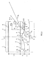
- FIGs.1 to 3 show an illumination unit 1 and surface light source device 2 included in the illumination unit 1 which are employed in this embodiment.
- FIG.1 is a plan view illustrating a surface light source device 2 and illumination unit 1, with a member such as LCD panel 3 to be illuminated being not shown.
- FIG.2 is a cross section view of the illumination unit shown in FIG.1 along X1-X1.
- FIG.3 is a partial cross section view of the illumination unit 1 along a plane on which optical axis L of LED 5 extends, giving a partial and enlarged illustration of FIG.2 in order to illustrate details of a configuration of recess 7.
- illumination unit 1 comprises light flux control member 4, a plurality of point-like light sources 5 arranged at a generally constant intervals on the side of back face 4a of light flux control member 1, light diffusion member 6 and a member 3 to be illuminated.
- Members 3 and 6 are disposed separately from emission face 4b, providing a gap between members 3, 6 and emission face 4b.
- Light flux control member 4 has a shape like a rectangular plate.
- point-like light sources 5 are LEDs (light emitting diodes).
- Surface light source device 2 is composed of light flux control member 4 and LEDs 5.
- Thin plate-like light flux control member 4 is made of transparent resin such as PMMA (polymethyl methacrylate) or PC (polycarbonate), or transparent glass, having emission face 4b and back face 4a.
- Back face 4a is provided with recesses 7 each of which faces each LED 5 correspondingly.
- Each recess 7 consists of first light inputting face 7a, which is spherical, and a second light inputting face 7b connecting the peripheral edge of the recess 7 with the area of the back face 4a around the recess 7.
- Light inputting face 7a provides a concave surface extending symmetrically with respect to optical axis L of LED 5.
- Second light inputting face 7b provides a convex surface curved in an opposite direction as compared with first light inputting face 7a. Accordingly, recess 7 has a point of inflection P at a portion connecting first and second light inputting faces 7a and 7b. It is noted that a direction giving the maximum emission intensity from LED 5 accords with optical axis L.
- reference plane C is defined a horizontal plane perpendicular to optical axis L of LED 5.
- Line A is defined as a line extends parallel with reference plane C as to pass position Pa at which light beam 5L emitted from LED 5 is incident to light flux control member 4. It is noted that light beam 5L generally represents emission from LED 5.
- incidence position Pa gives a point of intersection of cross section configuration line 7L of recess 7 shown in FIG.3 and light beam 5L.
- line B is a tangent of configuration line 7L of recess 7 at incidence position Pa. Tangent B and line A make angle ⁇ 3 which may be called " lens inclination angle" .
- Angle ⁇ 2 is an angle which light beam 5L makes with respect to normal VL of emission face 4b just before being outputted from light flux control member 4.
- angle ⁇ 5 is an emission angle from emission face 4b which light beam 5L makes with respect to normal VL of emission face 4b after being outputted from light flux control member 4.
- LED 5 has the maximum emission intensity direction according with optical axis L.
- the maximum emission intensity direction is also a direction along a normal of emission face 4b of light flux control member 4.
- Emission intensity of LED 5 falls gradually according to an increasing angular deviation from the maximum emission intensity direction; in other words, from the direction of optical axis L or the normal.
- half-intensity-angular-range is defined as an angular range extending up to an intensity-falling of 50% as compared with the maximum emission intensity from the maximum emission intensity direction.
- Recess 7 is configured so as to satisfy the following Conditions 1 and 2 for "light which is emitted toward within a certain angular range at least including half-intensity-angular-range from LED 5" .
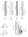
- FIG.4 is a diagram illustrating a relation between LED-emission angle ⁇ 1 and emission angle ⁇ 5 for light flux control member 4.
- the above " certain angular range at least including half-intensity-angular-range” is exemplarily shown as a range of ⁇ 1 satisfying a relation ⁇ 1 ⁇ ⁇ 1.
- Curve 8A in FIG.4 shows an example of relation between ⁇ 1 and ⁇ 5 that satisfies the above Conditions 1 and 2.
- angles ⁇ 2 and ⁇ 3 are expressed as the following Formulae 1 and 2, wherein n is refractive index of light flux control member 4.
- General operations light flux control member 4 having recess 7 configurated as above are as follows.
- light beam 5L generally representing emission from LED 5 enters into light flux control member 4 through recess 7.
- Refraction occurring at recess 7 involves expansion of travelling directions of light fluxes represented by light beam 5L.
- Light fluxes having expanded travelling directions are emitted from emission face 4b of light flux control member 4 towards the ambient (air) according to Snell's Law.
- back face 4a were flat (without recess 7), refraction occurs at back face 4a too, but expansion of light travelling directions occurs little.
- ⁇ 5 a is an angle made by imaginary light beam 5La with respect to a normal of emission face 4b.
- the present invention enables much expanded light fluxes to be outputted as compared with cases where no recess 7 is formed.
- Recess 7 of light flux control member 4 has sizes, such as the maximum diameter and depth d, and shapes of first and second light inputting faces 7a, 7b, which are determined preferably depending on factors such as emission characteristics (including angular emission range; half-intensity-angular-range), distance L1 between LED 5 and light flux control member 4, arrangement pitch (interval) of LEDs 5 p, thickness of light flux control member t, and distance L2 between emission face 4b and light diffusion member 6. It is noted that the maximum diameter is outermost diameter of second light inputting face 7b.
- a periphery portion of second light inputting face 7b is smoothly coupled with a generally flat configuration of back face 4a at a position to which a light beam of ⁇ 1 approximately equal to 7 5° is incident.
- FIG.5 illustrates a relation between LED emission angle ⁇ 1 and lens-face inclination angle ⁇ 3 in an illustration manner similar to FIG.4 .
- First light inputting face 7a of recess 7 shown in FIG.3 is formed, as illustrated by curve 8B in FIG.5 , corresponding to an angular range along a curving part in which ⁇ 3 increases according to increasing of ⁇ 1 (corresponding to a range in which ⁇ 1 is smaller than about 30° ).
- second light inputting face 7b of recess 7 is formed, as illustrated by curve 8B in Fig.5 , corresponding to another angular range along another curving part in which ⁇ 3 decreases according to increasing of ⁇ 1 (corresponding to a range in which ⁇ 1 changes from about 30° to 75° ).
- recess 7 is configurated so that ⁇ 3 is about 30° when ⁇ 1 is about 30°.
- curving part includes smooth curve and other similar lines, such as successively connected extremely short linear lines or an approximately curved line having a linear part, so far as they look like " curve " as a whole.
- emission angle ⁇ 5 of emission from emission face 4b increases smoothly and gradually from 0° to about 75° as to depict an upward- convex curve 8A as shown in FIG.4 .
- curve 8A accords with line 10 showing an imaginary relation between ⁇ 1 and ⁇ 5 under an imaginary condition without recess 7.
- Curve 8A is an upward-convex curve as a whole, being allowed to include a limer-line-like part.
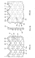
- FIGs.7 to 10 are plan views of first to fourth modifications of light flux control member 4, respectively.
- Light flux control member 4 shown in FIG.7 is formed of a plate like member looking like one shown in FIG.1 as a whole, which is composed of a plurality of light flux control member fragments 11a connected to each other. Each fragment 11a corresponds to each LED 5.
- light flux control members 4 shown in FIGs.8 to 10 are formed of plate like members looking like one shown in FIG.1 as a whole, each of which is composed of a plurality of light flux control member fragments 11b ( FIG.8 ), 11c ( FIG.9 ) or 11d ( FIG.10 ) connected to each other.
- Each fragment 11a corresponds to each LED 5.
- Each fragment 11b, 11c or 11d corresponds to each LED 5.
- each fragment 11a is shaped like equilateral hexagon, being fixed with light permeable adhesives (such as LTV-setting agent).
- Each fragment 11a has one recess 7 corresponding to each LED 5 on a back face opposite to an emission face of the instant light flux control member.
- each fragment 11b is shaped like slender hexagon, being fixed with light permeable adhesives (such as UV-setting agent).
- Each fragment 11b has one recess 7 corresponding to each LED 5 on a back face opposite to an emission face of the instant light flux control member.
- each fragment 11c is shaped like square, being fixed with light permeable adhesives (such as UV-setting agent). Fragments 11c are connected to each other so that fragments 11c in a row and ones in upper or lower adjacent row are shifted mutually by a pitch of half fragment size. Each fragment 11c has one recess 7 corresponding to each LED 5 on a back face opposite to an emission face of the instant light flux control member.
- light permeable adhesives such as UV-setting agent
- each fragment 11d is also shaped like square, being fixed with light permeable adhesives (such as UV- setting agent) as to be aligned lengthwise and crosswise.
- light permeable adhesives such as UV- setting agent
- each LED 5 is arranged generally corresponding to an area-center of each fragment shaped like hexagon or square.
- Each recess 7 is formed on a back face of fragment 11a, 11b 11c or 11d as to provide a concave configuration symmetric with respect to optical axis L of LED 5. It is noted that recess 7 may have a periphery edge shape other than circle-like shape (point- symmetric with respect to optical axis L), for instance, ellipse-like shape.
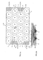
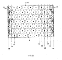
- Light flux control member assembly 25 having a large emission face.
- Light flux control member assembly 25 is composed of first to fourth light flux control members 20 5 to 23.
- the light flux control member assembly 25 is called simply "assembly 25".
- First and fourth light flux control members 20 and 23 have the same shape and second and third light flux control members 21 and 22 have the same shape.
- assembly 25 is composed of two kinds of light flux control members 20 ,23 and 21, 22.
- Engaging portion 26 of first and second light flux control members 20, 21 and engaging portion 27 of third and fourth fcs 22, 23 are divided into two parts, upper face side part and lower face side part, with a boundary at a middle position along the thickness direction.
- Projecting portion 28 shaped like trapezoid provided by three sides of hexagon formed in the lower face side part is engaged with recessing portion 30.
- arc-like projecting portion 31 formed in the upper face side part is engaged with recessing portion 32.
- top portions of trapezoid-like projecting portion 28 and arc-like projecting portion 31 roughly correspond to each other while bottom portions of trapezoid-like recessing portion 30 and arc-like recessing portion 32 roughly correspond to each other.
- a set of light flux control members 20, 21 engaged with each other and another set of light flux control members 22, 23 engaged with each other are supported by triangle-like corner fillet portions 33 from the lower side at engaging portions 26, 27, respectively. Corner fillet portions 33 are provided by corners of bottom portion of arc-like recessing portion 32 and trapezoid-like recessing portion 30.
- Such structure prevents first and second light flux control members 20, 21 and third and forth light flux control members 22, 23 to slide along a thickness direction of light flux control members 20 to 23.
- Engaging portion 34 of first and third light flux control members 20, 22 and engaging portion 35 of second and forth light flux control members 21, 23 are divided into two parts, upper face side part and lower face side part with a boundary at a middle position along thickness direction.
- Projecting portion 36 shaped like triangle provided by two sides of hexagon formed in the lower face side part is engaged with recessing portion 37.
- arc-like projecting portion 38 formed in the upper face side part is engaged with recessing portion 40.
- top portions of arc-like projecting portion 38 and triangle-like projecting portion 36 provide corner fillet portion 41 with which triangle-like projection portions 36 of light flux control members 20, 21, 22 or 23 to be engaged with as to be supported from the lower side.
- Such structure prevents first and third 20, 22 and second and forth light flux control members 21, 23 to slide along a thickness direction of light flux control members 20 to 23.
- An oblique side 42 of hexagon butts against first and fourth light flux control members 20, 23 roughly at a center position of light flux control member assembly 25.
- supporting projections 44 for supporting light flux control members 20 to 23 are arranged around recesses 7, respectively, as to abut against substrate not shown.
- Each of engaging portions 26, 27, 34 and 35 is fixed by light permeable adhesives such as UV-setting agent.
- a member such as frame member may be employed for holding the light flux control members.
- Light flux control assembly 25 constructed as above enables a backlighting arrangement (surface light source device) for large screen monitor display to be manufactured. It should be noted that assembly 25 may be composed of other numbers of fcs, for instance, two, three, five or more.
- FIGs.13a, 13b, 13c, 13d, 13e and 13f are side views of light diffusion members 6 in accordance with to first, second, third, forth, fifth and sixth examples, respectively. Any of illustrated light diffusion members 6 can be arrange at the emission face side of light flux control member 4.
- Each light diffusion member 6 is a sheet-like or plate-like member made of light well-permeable resin such as PMMA (polymethyl methacrylate) or PC (polycarbonate), having an area size generally equal to that of member 3 to be illuminated such as LCD panel, advertising display panel.
- PMMA polymethyl methacrylate
- PC polycarbonate
- Light diffusion member 6 shown in FIG.13a employs sheet- like base material 6a to both faces of which processing for giving light diffusion ability, such as emboss-pracessing or bead-processing, is applied.
- both faces of light diffusion member 6 are provided with fine uneven configurations 6b.
- Light diffusion member 6 shown in FIG.13b employs sheet-like base material 6a to both faces of which processing for giving light diffusion ability, such as emboss- processing or bead-processing, is applied.
- both faces of light diffusion member 6 are provided with fine uneven configurations 6b.
- light diffusive material 6c is dispersed within base material 6a.
- Light diffusion member 6 shown in FIG.13c employs sheet-like base material 6a to only an inner face of which processing for giving light diffusion ability, such as emboss-processing or bead-processing, is applied to form a fine uneven configuration 6b. It is noted that the inner face of light diffusion member 6 is a face directed to light flux control member 4. In addition, other face of light diffusion member 6 is provided with a great number of repeated prismatic projections 6d extending along a direction perpendicular to the paper surface.
- Light diffusion member 6 shown in FIG.13d is the same as one shown in FIG.13c except that light diffusive material 6c is dispersed within base material 6a.
- processing such as emboss-processing or bead-processing is applied to one face directed to light flux control member 4 to form a fine uneven configuration 6b.
- the other face of light diffusion member 6 is provided with a great number of repeated prismatic projections 6d extending along a direction perpendicular to the paper surface.
- Each of prismatic projections 6d shown in FIGs.13c and 13d is shaped like triangle, for instance, like isosceles triangle.
- Light diffusion member 6 shown in FIG.13e employs sheet-like base material 6a on an emission side face of which circular-cone-like projections 6e for are formed to cause light transmitted through base material 6a to be diffused.
- Light diffusion member 6 shown in FIG.13f employs sheet-like base material 6a on an emission side face of which pyramid-like (such as triangle-pyramid-like, quadrangle-pyramid-like or hexangle-pyramid-like) projections 6f for are formed to cause light transmitted through base material 6a to be diffused.
- pyramid-like such as triangle-pyramid-like, quadrangle-pyramid-like or hexangle-pyramid-like projections 6f for are formed to cause light transmitted through base material 6a to be diffused.
- Every light diffusion member 6 as above transmits and diffuses light emitted from emission face 4b of light flux control member 4, causing member 3 to be illuminated uniformly.
- every light diffusion member 6 as above may be mounted on an inner face directed to light flux control member 4 of member 3 to be illuminated, or alternatively, may be interposed between light flux control member 4 and member 3 to be illuminated, with being separated from member 3.
- FIGs.14a and 14b illustrate a first modification of surface light source device 2 and illumination unit 1 to which the present invention is applicable, wherein FIG.14a is a plan view in which a member to be illuminated and light diffusion member is not shown and FIG.14b is a cross section view along X2-X2 in FIG.14a .
- Frame 45 is a frame accommodating light flux control member 4
- LED 5 abuts on side face 46 of frame 45, some light from the same LED 5 is possibly reflected by side face 46 and emitted from emission face 47 near to side face 46.
- Light shielding processing may be performed by forming light- shielding- processed portion 48 partially on side face 46 in the vicinity of LED 5 that is close to side face ] 46.
- Light- shielding- processed portion 48 restrict reflection at side face 46 of frame 45.
- Black ink well absorbing light may be applied to side face 46 to form light- shielding- processed portion 48.
- a range covered by light-shielding-processed portion 48 is a certain region near to LED 5 close to side face 46, having a width generally equal to the maximum diameter of recess 7.
- Light- shielding- processed portion 48 has a covering range along height direction such that the range covers generally full height, as shown in FIG.14b .
- light- shielding- processed portion 48 covers, alternatively, only a part of full height.
- a specifically lowered voltage may be applied to LED 5 close to side face 46 to reduce emission intensity thereof instead of forming light- shielding- processed portion 48 on side face 46.
- Such an intensity-reduced emission of LED 5 avoids light reflected by side face 46 to disturb uniformity of emission intensity from emission face 47 of light flux control member 4.
- a light-shielding-processed portion may be formed on a side face of light flux control member 4 opposite to side face 46.
- a light diffusion member may be provided with a light-shielding-processed portion instead of that formed on frame 45 or light flux control member 4, for example, by printing. Any combination of the above arts of light-shielding or light-reducing may be employed.
- a light- shielding may be formed on a bottom of a frame or a reflection sheet.
- FIG. 15a and 15b illustrate a second modification of surface light source device 2 and illumination unit 1 to which the present invention is applicable, wherein FIG.15a is a plan view in which a member to be illuminated and light diffusion member is not shown and FIG.15b is a cross section view along X3-X3 in FIG.15a .
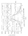
- FIG.16 is a diagram illustrating distributions of emission intensity of light from member 3 to be illuminated of illumination unit 1.
- curve A shows a distribution of emission intensity for a single LED 5 (point-like light source) disposed so as to be directed to a recess 7 configurated in accordance with the present invention on back face 4a of light flux control member 4.
- curve B shows a distribution of emission intensity in a case where a single LED 5 (point- like light source) is disposed as to be directed to back face 4a of light flux control member 4 having no recess.
- curve A tells that an increased intensity is realized at positions far from optical axis L as compared with that shown by curve B. Such an increased intensity can be estimated by difference ⁇ between A and B.
- FIGs.17a illustrated is an illumination unit 1 employing a light flux control member 4 provided with a recess configurated in accordance with the present invention while FIG.17b illustrates an illumination unit 1 employing a light flux control member 4 provided with a recess 60 configurated in accordance with a prior art.
- a distribution of emission intensity of illumination unit 1 shown in FIG.17b is depicted by curve C in FIG.16 .
- Curve C tells that a sharp rising of emission intensity occurs at a region Cl.
- a relation ( ⁇ 5 / ⁇ 1) > 1 is satisfied not only by employment of recess 7 in accordance with the present invention but also by employment of prior art recess 60 as shown in FIG.4 .
- ( ⁇ 5 / ⁇ 1) increases according to increasing of ⁇ 1 in the case of prior art recess 60.
- foresaid Condition 2 is not satisfied.
- prior art recess 7 having a conventional configuration involves a sharp changing of inclination to be coupled with a flat portion of back face 4a, failing to have a smooth coupling free from sharp changing of inclination.
- emission face 4b of light flux control member 4 As a result, it is difficult to output a uniformly expanded emission fluxes form emission face 4b of light flux control member 4 as illustrated in FIG.17b . In addition, some light travelled within light flux control member 4 is inner-reflected by emission face 4b without being outputted, reducing emission efficiency.
- curve D shows a distribution of emission intensity of light emitted from light diffusion member 6 in a case where a plurality of LEDs 5 (point- like light sources) are disposed at a certain interval as to be directed to corresponding recesses 7, respectively, configurated in accordance with the present invention on back face 4a of light flux control member 4 of illumination unit 1 which is constructed, for example, as shown un FIGs.1 and 2 .
- curve E shows a distribution of emission intensity in a case the same as the above illumination unit providing curve D except that no recess id formed on back face 4a of light flux control member 4.
- curve D shows a small variation of intensity and hardly involves a sharp changing as compared with that shown by curve E.
- illumination unit 1 in accordance with the present invention outputs much uniformalized light fluxes from light diffusion member 6 as compared with conventional illumination unit 1 providing curve E.
- curve F shows a distribution of emission intensity from light diffusion member 6 in a case where illumination unit 1 employing light flux control member 4 having a plurality of recesses 60 as shown in FIG.17b and LEDs 5 correspondingly.
- Curve F has a plurality of parts at which sharp and large intensity changes occur corresponding to LEDs 5 or recesses 60. To the contrary, curve D is almost free from sharp intensity changes and shows only small changes.
- recesses 7 enable light fluxes after being outputted from light flux control member 4 to be uniformly and effectively expanded. Light fluxes from LEDs adjacent to each other are well mixed, providing a uniform intensity emission as illustrated by curve D.
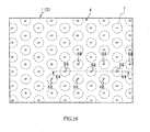
- FIGs.18 and 19 illustrate color-emission type surface light source device 2 and illumination unit 1 using the same to which the present invention is applicable.
- FIG.18 is a plan view illustrating color-emission type surface light source device 2 and illumination unit 1, with a member 3 to be illuminated and light diffusion member 6 being not shown.
- FIG.19 is a cross section view of illumination unit 1 shown in FIG.18 along X4-X4.
- Color-emission type surface light source device 2 is composed of light flux control member 4 and LEDs 5R, 5G and 5B. LEDs 5R, 5G and 5B are disposed alternately and emit red, green and blue light, respectively. Color light fluxes from LEDs 5R, 5G and 5B are introduced into light flux control member 4 through corresponding recesses 7, respectively.
- FIG.20 is a modification of a color- emission type surface light source device 2 and illumination unit 1 using the same.
- additional LEDs 5R, 5G and 5B (all of them or a part of them) to cover short of emission intensity.
- Such short of emission intensity of any color light from LED 5R, 5G or 5B tends to appear at regions near to left and right sides of light flux control member 4 shown in FIG. 20 .
- Additional LEDs may be mounted so that optical axes of them are inclined toward frame 70. If so mounted, light from the additional LEDs is reflected by corresponding inner surfaces of frame 70, being diffused widely. This causes light from the additional LEDs to be widespread.
- the additional LEDs may be supplied with electric current or voltage different from that with which the other LEDs are supplied in order to control emission intensity of additional LEDs.
- LEDs 5R, 5G or 5B are additionally arranged to the left and right sides of light flux control member 4. It is noted that further addition of LEDs may be adopted to cover other brightness-short regions.
- LEDs 5R, 5G or 5B may be arranged there.
- LED additional arrangement to light-short regions may be applied to cases where single-color emission is employed, in order to reduce unevenness of emission color.
- Recess or recesses 7 may be formed on emission face 4b as shown in FIG. 21a , though the invention is not concerned with this form. Alternatively, recess or recesses 7 may be formed on both faces 4a and 4b as shown in FIG. 21b .
- the optical axis L of each LED 5 has the same direction as a normal direction with respect to light flux control member 4 (or emission face 4b).
- this does not limit the scope of the present invention. That is, the optical axis L of LED 5 incorporated in a surface light source device or illumination unit can have some small deviation from the normal direction because of various factors such as unevenness of optical characteristics, quality, or assembly errors.
- the present invention can be applied to such cases without losing effects similar to those in the above embodiments obtained.
Description
- The present invention relates to a surface light source device, illumination unit and light flux control member, being applied, for instance, to a surface light source device for backlighting a liquid crystal display panel, an illumination unit adopting the surface light source device as an illuminating means, or a light flux control member employed in those. More specifically, surface light source devices, illumination units and light flux control members in accordance with the present invention are able to be applied to backlighting arrangements for TV's or personal computer monitor displays.
- A surface light source device employing a plurality of LEDs (light emitting diodes) as point-like light sources has been known as an illuminating means for a LCD monitor display of a personal computer or TV set. A plate-like light flux control member having roughly the same shape as that of a LCD panel is employed in the surface light source device, being provided with a plurality of LEDs arranged like a matrix at the back side. The LEDs emit light which is incident to a back face of the light flux control member and travels within the light flux control member to an emission face opposite to the back face, being outputted from the emission face toward a LCD panel to be backlighted. Prior arts like this have been disclosed in the following documents.
- This is found disclosed in
Tokkai 2002-49326 2002-49326 light source device 10 is provided withmicrolens array 102. Individual microlenses are arranged in one-to-one correspondence to a plurality ofLEDs 101, as shown inFIG.22 . Light fromLEDs 101 is outputted in a direction perpendicular to a plane (upward) viamicrolens array 102. - This is found disclosed in
Tokkaisho 59-226381 JP-A 1984-226381 emission display device 103 is provided withLED 104,concave lens 105 andconvex lens 106, as shown inFIG.23 . Light fromLED 104 is condensed byconvex lens 106 after being diverged byconcave lens 105, being outputted in a direction roughly parallel with an " optical axis " ofLED 104. Please note that "optical axis " is defined as a light travelling direction at a center of three-dimensional light flux emitted from a point-like light source (LED 104). - This is found disclosed in
Tokkaisho 63-6702 JP-A 1988-6702 illumination unit 107 having LED(s) 108, as shown inFIG.24 . Light fromLED 108 is condensed bycondenser lens 110 and directed forward, then being diverged by diverginglens 111. - Another prior art provides
illumination unit 1 as shown inFIG.17b . -
Illumination unit 1 is provided with lightflux control member 4 andLED 5 which is arranged at the side ofback face 4a of lightflux control member 4. Backface 4a has a semi-spherical recess 60 facing toLED 5 so that light fromLED 5 enters into lightflux control member 4 viarecess 60. The light is outputted fromemission face 4b. - However, the above prior arts involve problems as follows.
- Surface
light source device 100 has a portion at which configuration ofmicrolens array 102 varies discontinuously. The portion is located betweenLEDs 101 adjacent to each other. Emission intensity changes sharply at this discontinuity portion, with the result that a conspicuous unevenness in brightness appears around boundary regions between individual microlenses ofmicrolens array 102. - It is difficult to say that
concave lenses 105 inemission display 103 are coupled with each other continuously to form a plane. Further to this,convex lenses 106 are scarcely coupled with each other continuously to form a plane. Therefore, a member of a large area to be illuminated, such as large-screen liquid crystal display panel, is hardly supplied with uniform illumination light. - With
illumination unit 107, light fromLED 108 is diverged by diverginglens 111 after being condensed bycondenser lens 110. This wil reduce unevenness in brightness as compared with PriorArt 1. However, a sufficient mixing of light fluxes fromLEDs 108 adjacent to each other is hardly expected, with the result that unevenness in emission color betweenindividual LEDs 108 tends to be conspicuous. - With
illumination unit 1,emission angle θ 1 at emission fromLED 5 andemission angle θ 5 at emission from lightflux control member 4 satisfy arelation θ 5 /θ 1 > 1 for light fromLED 5 other than light within an angular neighbourhood of a normal direction as illustrated inFIGs17b and4 . Please note that " normal direction " is defined as a direction which accords with optical axis L inFIG.17b and a normal perpendicular toemission face 4b of lightflux control member 4. In other words,emission angle θ 1 at emission fromLED 2 is greater thanemission angle θ 5 at emission from lightflux control member 4. This enables emission fluxes fromLED 5 to be converted into expanded emission fluxes. - However, an incidence to an end edge of a
recess 60 brings light that intersects with light brought by incidence to a neighbourhood of the end edge because the end edge of recess 60 (connecting portion between semi-sphere-like recess 60 and generally flat backface 4a) gives a sharp edge. This intersection of light raises a problem of ring-like emission. As a result,illumination unit 1 fails to expand light fromLED 5 smoothly and effectively to a desirable range. -
JP 06-349305-A DE 19621148 (Magna Reflex Holding) shows a flexible light guide with recesses and resting on a circuit board, used for an automobile light. - An object of the present invention is to provide a surface light source device employing a plurality of point-like light sources such as LEDs, and an illumination unit using the surface light source device, in which there is no conspicuous unevenness of emission color or irregular brightness.
- Embodiments of the present invention should enable such a surface light source device employing point-like light sources such as LEDs, and an illumination unit including the surface light source device, to expand light from the point-like light sources smoothly and effectively to a desirable range.
- According to the present invention there is provided a surface light source device as defined in
claim 1. - An illumination unit may be provided employing the surface light source device and a light diffusion member.
- According to the present invention, light fluxes from a point-like light source are expanded smoothly and effectively to a wide range by the recesses corresponding to the LEDs. As a result, illumination light emitted from an emission face of the light flux control member has a uniform brightness over a wide range.
- Since a plurality of point-like light sources is employed, the light fluxes from them tend to be well mixed. Therefore, if differences in emission color exist, emission from the light flux control member not only tends to be free from the differences but also shows a high uniformity of brightness.
- For a better understanding of the invention, embodiments of it will now be described, by way of example, with reference to the accompanying drawings, in which:
-
FIG.1 is a plan view illustrating a surface light source device and illumination unit to which the present invention is applicable, with a member to be illuminated and light diffusion member being not shown;FIG.2 is a cross section view of the illumination unit shown inFIG.1 along X1-X1;FIG.3 is a partial cross section view of the illumination unit along a plane on which an optical axis of a LED extends, giving a partial and enlarged illustration ofFIG.2 in order to illustrate details of a recess configuration; -
FIG.4 is a diagram illustrating a relation between LED-emission angle θ 1 andemission angle θ 5 for a light flux control member; -
FIG.5 is a diagram illustrating a relation between LEDemission angle θ 1, and lens-faceinclination angle θ 3 for the light flux control member; -
FIG.6 is a cross section view of an illumination unit in accordance with a first embodiment; -
FIG.7 is a plan view of a light flux control member in accordance with a first modification; -
FIG.8 is a plan view of a light flux control member in accordance with a second modification; -
FIG.9 is a plan view of a light flux control member in accordance with a third modification; -
FIG.10 is a plan view of a light flux control member in accordance with a forth modification; -
FIG.11 is a plan view of a light flux control member assembly having a large emission face, which is produced by combining a plurality of light flux control members; -
FIGs.12a, 12b and 12c are a back plan view, side view and plan view of a light flux control member employed in a light flux control member assembly, respectively; -
FIGs.13a, 13b, 13c, 13d, 13e and 13f are side views of light diffusion members in accordance with to first, second, third, forth, fifth and sixth examples, respectively, andFIG.13g is an enlarged partial view of illumination unit in which light diffusion members shownFIGs.13a to 13f are tobe employed; -
FIGs.14a and 14b illustrate a first modification of surface light source device and illumination unit to which the present invention is applicable, whereinFIG.14a is a plan view in which a member to be illuminated and light diffusion member is not shown andFIG.14b is a cross section view along X2-X2 inFIG.14a ; -
FIGs.15a and 15b illustrate a second modification of surface light source device and illumination unit to which the present invention is applicable, whereinFIG.15a is a plan view in which a member to be illuminated and light diffusion member is not shown andFIG. 15b is a cross section view along X3-X3 inFIG. 14a ; -
FIG. 16 is a diagram illustrating distributions of emission intensity from a member to be illuminated of an illumination unit to which the present invention is applied; -
FIG. 17a illustrates an illumination unit (single light source) employing a light flux control member provided with a recess configured in accordance with the present invention andFIG. 17b illustrates an illumination unit (single light source) employing a light flux control member provided with a recess configurated in accordance with a prior art (fourth prior art), for comparison; -
FIG. 18 is a plan view illustrating a color-emission type surface light source device and illumination unit using the same to which the present invention is applicable, with a member to be illuminated and light diffusion member not being shown; -
FIG. 19 is a cross section view of the illumination unit shown inFIG. 18 along X4-X4; -
FIG. 20 is a plan view of a modification of a color-emission type surface light source device and illumination unit using the same to which the present invention is applicable, wherein a member to be illuminated and light diffusion member are not shown; -
FIG. 21a is a partial cross section view, solely for reference, of an illumination unit in which recesses are formed on an emission face of the light flux control member, and -
FIG. 21b is a partial cross section view of an illumination unit embodying the invention, in which recesses are formed on both an emission face and back face; -
FIG. 22 is a diagram illustrating a structure of a first prior art; -
FIG. 23 is a diagram illustrating a structure of a second prior art; and -
FIG. 24 is a diagram illustrating a structure of a third prior art. -
FIGs.1 to 3 show anillumination unit 1 and surfacelight source device 2 included in theillumination unit 1 which are employed in this embodiment.FIG.1 is a plan view illustrating a surfacelight source device 2 andillumination unit 1, with a member such asLCD panel 3 to be illuminated being not shown.FIG.2 is a cross section view of the illumination unit shown inFIG.1 along X1-X1.FIG.3 is a partial cross section view of theillumination unit 1 along a plane on which optical axis L ofLED 5 extends, giving a partial and enlarged illustration ofFIG.2 in order to illustrate details of a configuration ofrecess 7. - Referring to
FIGs.1 to 3 ,illumination unit 1 comprises lightflux control member 4, a plurality of point-like light sources 5 arranged at a generally constant intervals on the side ofback face 4a of lightflux control member 1,light diffusion member 6 and amember 3 to be illuminated.Members emission face 4b, providing a gap betweenmembers emission face 4b. Lightflux control member 4 has a shape like a rectangular plate. In this embodiment, point-like light sources 5 are LEDs (light emitting diodes). Surfacelight source device 2 is composed of lightflux control member 4 andLEDs 5. - Thin plate-like light
flux control member 4 is made of transparent resin such as PMMA (polymethyl methacrylate) or PC (polycarbonate), or transparent glass, havingemission face 4b and backface 4a.Back face 4a is provided withrecesses 7 each of which faces eachLED 5 correspondingly. Eachrecess 7 consists of firstlight inputting face 7a, which is spherical, and a secondlight inputting face 7b connecting the peripheral edge of therecess 7 with the area of theback face 4a around therecess 7. -
Light inputting face 7a provides a concave surface extending symmetrically with respect to optical axis L ofLED 5. Secondlight inputting face 7b provides a convex surface curved in an opposite direction as compared with firstlight inputting face 7a. Accordingly,recess 7 has a point of inflection P at a portion connecting first and second light inputting faces 7a and 7b. It is noted that a direction giving the maximum emission intensity fromLED 5 accords with optical axis L. - In
FIG.3 , reference plane C is defined a horizontal plane perpendicular to optical axis L ofLED 5. Line A is defined as a line extends parallel with reference plane C as to pass position Pa at whichlight beam 5L emitted fromLED 5 is incident to lightflux control member 4. It is noted thatlight beam 5L generally represents emission fromLED 5. - It is also noted that incidence position Pa gives a point of intersection of cross
section configuration line 7L ofrecess 7 shown inFIG.3 andlight beam 5L. In addition, line B is a tangent ofconfiguration line 7L ofrecess 7 at incidence position Pa. Tangent B and line Amake angle θ 3 which may be called " lens inclination angle" . -
Light beam 5L travelling within lightflux control member 4 makes an incidence angle (inner incidence angle)θ 2 on impinging uponemission face 4b.Angle θ 2 is an angle whichlight beam 5L makes with respect to normal VL ofemission face 4b just before being outputted from lightflux control member 4. Finally,angle θ 5 is an emission angle fromemission face 4b whichlight beam 5L makes with respect to normal VL ofemission face 4b after being outputted from lightflux control member 4. - An angular range called " half-intensity-angular-range " is introduced for
LED 5 in order to describe optical conditions to be satisfied byrecess 7. - As mentioned previously,
LED 5 has the maximum emission intensity direction according with optical axis L. The maximum emission intensity direction is also a direction along a normal ofemission face 4b of lightflux control member 4. Emission intensity ofLED 5 falls gradually according to an increasing angular deviation from the maximum emission intensity direction; in other words, from the direction of optical axis L or the normal. - Under such situation, " half-intensity-angular-range " is defined as an angular range extending up to an intensity-falling of 50% as compared with the maximum emission intensity from the maximum emission intensity direction.
-
Recess 7 is configured so as to satisfy the followingConditions LED 5" . - ● Condition 1:
Relation θ 5 /θ 1 > 1 is satisfied except for light emitted toward within an angular-neighborhood of a normal direction with respect to emission face 4B. It is noted that " angular- neighborhood of a normal direction " is preferably an angular range within 5 degrees (± 5° ) from the direction of optical axis L. - ●
Condition 2; Value ofθ 5 /θ 1 falls gradually according to increasing ofθ 1. -
FIG.4 is a diagram illustrating a relation between LED-emission angle θ 1 andemission angle θ 5 for lightflux control member 4. InFIG.4 , the above " certain angular range at least including half-intensity-angular-range " is exemplarily shown as a range ofθ 1 satisfying arelation θ 1 <α 1. - Curve 8A in
FIG.4 shows an example of relation betweenθ 1 andθ 5 that satisfies theabove Conditions Dotted line 10 inFIG.4 shows an equation (θ5/θ1) = 1. - It is noted that
angles θ 2 andθ 3 are expressed as the followingFormulae flux control member 4.

- Thus relation between
θ 3 andθ 1 is shown bycurve 8B inFIG.5 .Curve 8B tells thatθ 3 increases gradually according to increasing ofθ 1 untilθ 1 =θ 3 =α 2 is satisfied. It is noted thatθ 3 decreases gradually according to increasing ofθ 1 in arange θ 1 >α 2. - General operations light
flux control member 4 havingrecess 7 configurated as above are as follows. - As illustrated in
FIG.3 ,light beam 5L generally representing emission fromLED 5 enters into lightflux control member 4 throughrecess 7. Refraction occurring atrecess 7 involves expansion of travelling directions of light fluxes represented bylight beam 5L. Light fluxes having expanded travelling directions are emitted fromemission face 4b of lightflux control member 4 towards the ambient (air) according to Snell's Law. - If the
back face 4a were flat (without recess 7), refraction occurs atback face 4a too, but expansion of light travelling directions occurs little. - Therefore, if an imaginary incident light beam 5La is introduced under existence of such an imaginary flat face, the emission angle of the imaginary beam 5La, θ5a, will satisfy
θ 5 a <θ 5 . It is noted thatθ 5 a is an angle made by imaginary light beam 5La with respect to a normal ofemission face 4b. - As understood from the above explanation, the present invention enables much expanded light fluxes to be outputted as compared with cases where no
recess 7 is formed. - As a result, some of light fluxes from " a
LED 5 " having LEDemission angle θ 1 within half-intensity-angular-range can come, after being outputted fromemission face 4b, for example, up to a position corresponding to an intersection point oflight diffusion member 6 and optical axis L of adistant LED 5 beyond anadjacent LED 5 that is adjacent to the above " aLED 5 " as shown inFIG.2 . - In the next place, examples of light
flux control member 4 are described by referring toFIGs.4 to 6 . -
Recess 7 of lightflux control member 4 has sizes, such as the maximum diameter and depth d, and shapes of first and second light inputting faces 7a, 7b, which are determined preferably depending on factors such as emission characteristics (including angular emission range; half-intensity-angular-range), distance L1 betweenLED 5 and lightflux control member 4, arrangement pitch (interval) of LEDs 5 p, thickness of light flux control member t, and distance L2 betweenemission face 4b andlight diffusion member 6. It is noted that the maximum diameter is outermost diameter of secondlight inputting face 7b. - Referring to
FIG.6 showing an example, lightflux control member 4 is made of transparent resin material having refractive index n=1.49, andL 1 =3.72mm, p =24.25mm, t =3.28mm,L 2 =9.0mm and d =2.28mm. - A periphery portion of second
light inputting face 7b is smoothly coupled with a generally flat configuration ofback face 4a at a position to which a light beam ofθ 1 approximately equal to 7 5° is incident. - This will be understood by referring to
line 8B shown inFIG.5. FIG.5 illustrates a relation between LEDemission angle θ 1 and lens-faceinclination angle θ 3 in an illustration manner similar toFIG.4 . - First
light inputting face 7a ofrecess 7 shown inFIG.3 is formed, as illustrated bycurve 8B inFIG.5 , corresponding to an angular range along a curving part in whichθ 3 increases according to increasing of θ 1 (corresponding to a range in whichθ 1 is smaller than about 30° ). - On the other hand, second
light inputting face 7b ofrecess 7 is formed, as illustrated bycurve 8B inFig.5 , corresponding to another angular range along another curving part in whichθ 3 decreases according to increasing of θ 1 (corresponding to a range in which θ 1 changes from about 30° to 75° ). -
Curve 8B has a point of inflection roughly corresponding to a point ofθ 1 = 30° , changing from " increasing " to " decreasing " at the point of inflection. It is noted that first and second light inputting faces 7a and 7b are connected to each other at the point of inflection. - In the illustrated example,
recess 7 is configurated so thatθ 3 is about 30° whenθ 1 is about 30°. - It is noted that " curving part " includes smooth curve and other similar lines, such as successively connected extremely short linear lines or an approximately curved line having a linear part, so far as they look like " curve " as a whole.
- If
recess 7 is formed as above,emission angle θ 5 of emission fromemission face 4b increases smoothly and gradually from 0° to about 75° as to depict an upward- convex curve 8A as shown inFIG.4 . - At about 75°, curve 8A accords with
line 10 showing an imaginary relation between θ1 and θ5 under an imaginary condition withoutrecess 7. Curve 8A is an upward-convex curve as a whole, being allowed to include a limer-line-like part. -
FIGs.7 to 10 are plan views of first to fourth modifications of lightflux control member 4, respectively. - Light
flux control member 4 shown inFIG.7 is formed of a plate like member looking like one shown inFIG.1 as a whole, which is composed of a plurality of light fluxcontrol member fragments 11a connected to each other. Eachfragment 11a corresponds to eachLED 5. - In similar ways, light
flux control members 4 shown inFIGs.8 to 10 are formed of plate like members looking like one shown inFIG.1 as a whole, each of which is composed of a plurality of light flux control member fragments 11b (FIG.8 ), 11c (FIG.9 ) or11d (FIG.10 ) connected to each other. Eachfragment 11a corresponds to eachLED 5. Eachfragment LED 5. - As illustrated in
FIG.7 , eachfragment 11a is shaped like equilateral hexagon, being fixed with light permeable adhesives (such as LTV-setting agent). Eachfragment 11a has onerecess 7 corresponding to eachLED 5 on a back face opposite to an emission face of the instant light flux control member. - As illustrated in
FIG.8 , eachfragment 11b is shaped like slender hexagon, being fixed with light permeable adhesives (such as UV-setting agent). Eachfragment 11b has onerecess 7 corresponding to eachLED 5 on a back face opposite to an emission face of the instant light flux control member. - As illustrated in
FIG.9 , eachfragment 11c is shaped like square, being fixed with light permeable adhesives (such as UV-setting agent).Fragments 11c are connected to each other so thatfragments 11c in a row and ones in upper or lower adjacent row are shifted mutually by a pitch of half fragment size. Eachfragment 11c has onerecess 7 corresponding to eachLED 5 on a back face opposite to an emission face of the instant light flux control member. - As illustrated in
FIG.10 , eachfragment 11d is also shaped like square, being fixed with light permeable adhesives (such as UV- setting agent) as to be aligned lengthwise and crosswise. - In first to fourth modifications, each
LED 5 is arranged generally corresponding to an area-center of each fragment shaped like hexagon or square. Eachrecess 7 is formed on a back face offragment 11b LED 5. It is noted thatrecess 7 may have a periphery edge shape other than circle-like shape (point- symmetric with respect to optical axis L), for instance, ellipse-like shape. - Referring to
FIGs.11 and12a to 12c , light fluxcontrol member assembly 25 having a large emission face. Light fluxcontrol member assembly 25 is composed of first to fourth lightflux control members 20 5 to 23. The light fluxcontrol member assembly 25 is called simply "assembly 25". First and fourth lightflux control members flux control members assembly 25 is composed of two kinds of lightflux control members - Engaging
portion 26 of first and second lightflux control members portion 27 of third andfourth fcs - Projecting
portion 28 shaped like trapezoid provided by three sides of hexagon formed in the lower face side part is engaged with recessingportion 30. Similarly, arc-like projectingportion 31 formed in the upper face side part is engaged with recessingportion 32. - As illustrated in
FIGs.11 and12a to 12c , top portions of trapezoid-like projectingportion 28 and arc-like projectingportion 31 roughly correspond to each other while bottom portions of trapezoid-like recessing portion 30 and arc-like recessing portion 32 roughly correspond to each other. - A set of light
flux control members flux control members corner fillet portions 33 from the lower side at engagingportions Corner fillet portions 33 are provided by corners of bottom portion of arc-like recessing portion 32 and trapezoid-like recessing portion 30. - Such structure prevents first and second light
flux control members flux control members flux control members 20 to 23. - Engaging
portion 34 of first and third lightflux control members portion 35 of second and forth lightflux control members - Projecting
portion 36 shaped like triangle provided by two sides of hexagon formed in the lower face side part is engaged with recessing portion 37. Similarly, arc-like projectingportion 38 formed in the upper face side part is engaged with recessingportion 40. - Further, as illustrated, top portions of arc-like projecting
portion 38 and triangle-like projectingportion 36 providecorner fillet portion 41 with which triangle-like projection portions 36 of lightflux control members - Such structure prevents first and third 20, 22 and second and forth light
flux control members flux control members 20 to 23. - An
oblique side 42 of hexagon butts against first and fourth lightflux control members control member assembly 25. - At the back face side of light
flux control members 20 to 23 (for example, at the side ofback face 23a knFIG.12a, 12b ) on which recesses are formed, supportingprojections 44 for supporting lightflux control members 20 to 23 are arranged aroundrecesses 7, respectively, as to abut against substrate not shown. - Each of engaging
portions - Light
flux control assembly 25 constructed as above enables a backlighting arrangement (surface light source device) for large screen monitor display to be manufactured. It should be noted thatassembly 25 may be composed of other numbers of fcs, for instance, two, three, five or more. -
FIGs.13a, 13b, 13c, 13d, 13e and 13f are side views oflight diffusion members 6 in accordance with to first, second, third, forth, fifth and sixth examples, respectively. Any of illustratedlight diffusion members 6 can be arrange at the emission face side of lightflux control member 4. - Each
light diffusion member 6 is a sheet-like or plate-like member made of light well-permeable resin such as PMMA (polymethyl methacrylate) or PC (polycarbonate), having an area size generally equal to that ofmember 3 to be illuminated such as LCD panel, advertising display panel. -
Light diffusion member 6 shown inFIG.13a employs sheet-like base material 6a to both faces of which processing for giving light diffusion ability, such as emboss-pracessing or bead-processing, is applied. Thus both faces oflight diffusion member 6 are provided with fineuneven configurations 6b. -
Light diffusion member 6 shown inFIG.13b employs sheet-like base material 6a to both faces of which processing for giving light diffusion ability, such as emboss- processing or bead-processing, is applied. Thus both faces oflight diffusion member 6 are provided with fineuneven configurations 6b. In addition, lightdiffusive material 6c is dispersed withinbase material 6a. -
Light diffusion member 6 shown inFIG.13c employs sheet-like base material 6a to only an inner face of which processing for giving light diffusion ability, such as emboss-processing or bead-processing, is applied to form a fineuneven configuration 6b. It is noted that the inner face oflight diffusion member 6 is a face directed to lightflux control member 4. In addition, other face oflight diffusion member 6 is provided with a great number of repeatedprismatic projections 6d extending along a direction perpendicular to the paper surface. -
Light diffusion member 6 shown inFIG.13d is the same as one shown inFIG.13c except that lightdiffusive material 6c is dispersed withinbase material 6a. In the same manner as the case ofFIG.13c , processing such as emboss-processing or bead-processing is applied to one face directed to lightflux control member 4 to form a fineuneven configuration 6b. The other face oflight diffusion member 6 is provided with a great number of repeatedprismatic projections 6d extending along a direction perpendicular to the paper surface. Each ofprismatic projections 6d shown inFIGs.13c and 13d is shaped like triangle, for instance, like isosceles triangle. -
Light diffusion member 6 shown inFIG.13e employs sheet-like base material 6a on an emission side face of which circular-cone-like projections 6e for are formed to cause light transmitted throughbase material 6a to be diffused. -
Light diffusion member 6 shown inFIG.13f employs sheet-like base material 6a on an emission side face of which pyramid-like (such as triangle-pyramid-like, quadrangle-pyramid-like or hexangle-pyramid-like)projections 6f for are formed to cause light transmitted throughbase material 6a to be diffused. - Every
light diffusion member 6 as above transmits and diffuses light emitted fromemission face 4b of lightflux control member 4, causingmember 3 to be illuminated uniformly. - It is noted that every
light diffusion member 6 as above may be mounted on an inner face directed to lightflux control member 4 ofmember 3 to be illuminated, or alternatively, may be interposed between lightflux control member 4 andmember 3 to be illuminated, with being separated frommember 3. -
FIGs.14a and 14b illustrate a first modification of surfacelight source device 2 andillumination unit 1 to which the present invention is applicable, whereinFIG.14a is a plan view in which a member to be illuminated and light diffusion member is not shown andFIG.14b is a cross section view along X2-X2 inFIG.14a . -
Frame 45 is a frame accommodating lightflux control member 4 - If
LED 5 abuts onside face 46 offrame 45, some light from thesame LED 5 is possibly reflected byside face 46 and emitted from emission face 47 near toside face 46. - Such emission could disturb light intensity distribution of emission from
emission face 47. Therefore it is preferable to apply light shielding processing to a portion aroundLED 5 onside face 46 on which thatLED 5 could abut. Light shielding processing may be performed by forming light- shielding- processedportion 48 partially onside face 46 in the vicinity ofLED 5 that is close to side face ] 46. Light- shielding- processedportion 48 restrict reflection atside face 46 offrame 45. Black ink well absorbing light may be applied toside face 46 to form light- shielding- processedportion 48. - In
FIGs. 14a , a range covered by light-shielding-processedportion 48 is a certain region near toLED 5 close toside face 46, having a width generally equal to the maximum diameter ofrecess 7. Light- shielding- processedportion 48 has a covering range along height direction such that the range covers generally full height, as shown inFIG.14b . - It is noted that light- shielding- processed
portion 48 covers, alternatively, only a part of full height. - It is also noted that a specifically lowered voltage may be applied to
LED 5 close toside face 46 to reduce emission intensity thereof instead of forming light- shielding- processedportion 48 onside face 46. Such an intensity-reduced emission ofLED 5 avoids light reflected byside face 46 to disturb uniformity of emission intensity from emission face 47 of lightflux control member 4. - A light-shielding-processed portion may be formed on a side face of light
flux control member 4 opposite toside face 46. - A light diffusion member may be provided with a light-shielding-processed portion instead of that formed on
frame 45 or lightflux control member 4, for example, by printing.
Any combination of the above arts of light-shielding or light-reducing may be employed. A light- shielding may be formed on a bottom of a frame or a reflection sheet. -
Figs. 15a and 15b illustrate a second modification of surfacelight source device 2 andillumination unit 1 to which the present invention is applicable, whereinFIG.15a is a plan view in which a member to be illuminated and light diffusion member is not shown andFIG.15b is a cross section view along X3-X3 inFIG.15a . - As shown in
FIGs.15a and 15b , noLED 5 is disposed in hatchedregions 50 to 53. In such situation, emission intensity from emission face 54 of lightflux control member 4 tends to be short in the vicinity ofregions 50 to 53. This lack of light is relaxed by forming anirregular reflection portion 55 which is formed by applying irregular-reflection-processing to hatchedregions 50 to 53 onemission face 54. Light reachingirregular reflection portion 55 form acorresponding LED 5 is irregularly reflected, providing a promoted emission. As a result, emission uniformity from emission face 54 is uniformalized. Irregular-reflection-processing may be performed by surface-roughening, applying irregular-reflection-mm or irregular-reflection-paint.Irregular reflection portion 55 is formed at least a position on any face of lightflux control member 4, preferably being formed on emission face, back face and side face of lightflux control member 4. -
FIG.16 is a diagram illustrating distributions of emission intensity of light frommember 3 to be illuminated ofillumination unit 1. - In
FIG.16 , curve A shows a distribution of emission intensity for a single LED 5 (point-like light source) disposed so as to be directed to arecess 7 configurated in accordance with the present invention onback face 4a of lightflux control member 4. - In
FIG.16 , curve B shows a distribution of emission intensity in a case where a single LED 5 (point- like light source) is disposed as to be directed to backface 4a of lightflux control member 4 having no recess. - Comparing curve A with curve B, curve A tells that an increased intensity is realized at positions far from optical axis L as compared with that shown by curve B. Such an increased intensity can be estimated by difference Δ between A and B.
- Referring to
FIGs.17a , illustrated is anillumination unit 1 employing a lightflux control member 4 provided with a recess configurated in accordance with the present invention whileFIG.17b illustrates anillumination unit 1 employing a lightflux control member 4 provided with arecess 60 configurated in accordance with a prior art. - A distribution of emission intensity of
illumination unit 1 shown inFIG.17b is depicted by curve C inFIG.16 . Curve C tells that a sharp rising of emission intensity occurs at a region Cl. - It can be said that such a sharp intensity rising is caused by emission light beams which are mutually intersected as shown by Y1 in
FIG.17b . - It should be noted that employment of
prior art recess 60 gives a relation betweenθ 1 andθ 3 , which is previously mentioned in connection withFIG.5 , such thatθ 3 increases in proportion to increasing ofθ 1. - A relation (
θ 5 / θ 1) > 1 is satisfied not only by employment ofrecess 7 in accordance with the present invention but also by employment ofprior art recess 60 as shown inFIG.4 . However, (θ 5 / θ 1) increases according to increasing ofθ 1 in the case ofprior art recess 60. In other words,foresaid Condition 2 is not satisfied. After all,prior art recess 7 having a conventional configuration involves a sharp changing of inclination to be coupled with a flat portion ofback face 4a, failing to have a smooth coupling free from sharp changing of inclination. - As a result, it is difficult to output a uniformly expanded emission fluxes form
emission face 4b of lightflux control member 4 as illustrated inFIG.17b . In addition, some light travelled within lightflux control member 4 is inner-reflected byemission face 4b without being outputted, reducing emission efficiency. - Such drawbacks of prior
art illumination unit 1 shown inFIG.17b are deleted byillumination unit 1 shown inFIG.17a employing lightflux control member 4 provided withrecess 7 configurated in accordance with the present invention. - That is, in the case of
illumination unit 1 shown inFIG.17a , for light which is emitted toward within a half- intensity- angular- range fromLED 5,relation θ 5 /θ 1 > 1 is satisfied except for light emitted toward within an angular-neighborhood of a normal direction with respect toemission face 4b, as shown inFIG.4 , and value ofθ 5 /θ 1 falls gradually according to increasing ofθ 1 . - This causes light fluxes after being outputted from light
flux control member 4 are light fluxes uniformly, effectively and smoothly expanded light fluxes as illustrated by curve A inFIG.16 . - In
FIG.16 , curve D shows a distribution of emission intensity of light emitted fromlight diffusion member 6 in a case where a plurality of LEDs 5 (point- like light sources) are disposed at a certain interval as to be directed tocorresponding recesses 7, respectively, configurated in accordance with the present invention onback face 4a of lightflux control member 4 ofillumination unit 1 which is constructed, for example, as shown unFIGs.1 and2 . - On the other hand, curve E shows a distribution of emission intensity in a case the same as the above illumination unit providing curve D except that no recess id formed on
back face 4a of lightflux control member 4. - Comparing curve D with curve E, curve D shows a small variation of intensity and hardly involves a sharp changing as compared with that shown by curve E.
- This tells that
illumination unit 1 in accordance with the present invention outputs much uniformalized light fluxes fromlight diffusion member 6 as compared withconventional illumination unit 1 providing curve E. - Next, curve F shows a distribution of emission intensity from
light diffusion member 6 in a case whereillumination unit 1 employing lightflux control member 4 having a plurality ofrecesses 60 as shown inFIG.17b andLEDs 5 correspondingly. - Curve F has a plurality of parts at which sharp and large intensity changes occur corresponding to
LEDs 5 or recesses 60. To the contrary, curve D is almost free from sharp intensity changes and shows only small changes. - Thus employment of
recesses 7 enables light fluxes after being outputted from lightflux control member 4 to be uniformly and effectively expanded. Light fluxes from LEDs adjacent to each other are well mixed, providing a uniform intensity emission as illustrated by curve D. - In addition, if there are emission color differences, such as differences in degree of being yellowish, between
LEDs 5, light fluxes fromLEDs 5 well mixed as above prevent the differences from looking conspicuous, providing a high quality illumination. -
FIGs.18 and19 illustrate color-emission type surfacelight source device 2 andillumination unit 1 using the same to which the present invention is applicable. -
FIG.18 is a plan view illustrating color-emission type surfacelight source device 2 andillumination unit 1, with amember 3 to be illuminated andlight diffusion member 6 being not shown.FIG.19 is a cross section view ofillumination unit 1 shown inFIG.18 along X4-X4. - Color-emission type surface
light source device 2 is composed of lightflux control member 4 andLEDs LEDs LEDs flux control member 4 throughcorresponding recesses 7, respectively. - As shown in
FIG.19 , fluxes near to an end ofleft side LED 5G reach the vicinity of an intersection of optical axis L ofright side LED 5G andlight diffusion member 6 across a range correspondingmiddle LED 5G. - In a such way, fluxes from
LEDs 5 are well mixed not only when all colors of LEDs are switched on but also when a single color of LEDs are switched on, with the result a uniform and excellent illumination is realized. -
FIG.20 is a modification of a color- emission type surfacelight source device 2 andillumination unit 1 using the same. - In this modification,
additional LEDs LED flux control member 4 shown inFIG. 20 . Additional LEDs may be mounted so that optical axes of them are inclined towardframe 70. If so mounted, light from the additional LEDs is reflected by corresponding inner surfaces offrame 70, being diffused widely. This causes light from the additional LEDs to be widespread. The additional LEDs may be supplied with electric current or voltage different from that with which the other LEDs are supplied in order to control emission intensity of additional LEDs. - In the modification shown in
FIG. 20 ,LEDs flux control member 4. It is noted that further addition of LEDs may be adopted to cover other brightness-short regions. - For example, if brightness-short regions exist at upper and lower sides of light
flux control member 4,additional LEDs - LED additional arrangement to light-short regions may be applied to cases where single-color emission is employed, in order to reduce unevenness of emission color.
- Recess or recesses 7 may be formed on
emission face 4b as shown inFIG. 21a , though the invention is not concerned with this form. Alternatively, recess or recesses 7 may be formed on bothfaces FIG. 21b . - In the above embodiments, the optical axis L of each
LED 5 has the same direction as a normal direction with respect to light flux control member 4 (oremission face 4b). However, this does not limit the scope of the present invention. That is, the optical axis L ofLED 5 incorporated in a surface light source device or illumination unit can have some small deviation from the normal direction because of various factors such as unevenness of optical characteristics, quality, or assembly errors. The present invention can be applied to such cases without losing effects similar to those in the above embodiments obtained.
Claims (3)
- A surface light source device (2), comprising a plurality of point-like light sources (5) and a light flux control member (4) having a back face (4a) in which is provided a plurality of recesses (7) for receiving, refracting and transmitting light from corresponding ones of said point-like light sources (5) which face respective ones of said recesses (7), the light flux control member (4) further comprising an emission face (4b) from which said light is emitted;
in which said back face (4a) has a flat area arranged to receive light from one or more of the light sources (5), and each said recess (7) has a first light-input face (7a), and a second light-input face (7b) a peripheral portion of which is smoothly connected to said flat area of said back face (4a), while said first and second light-input faces (7a, 7b) are interconnected at a connection location to provide a point of inflection (P) and are configured so as to satisfy the following Conditions 1 and 2, at least for light which is emitted within an angular range within a half-intensity angular range from said point-like source:Condition 1: the Relation θ5/θ1>1 is satisfied, except for light emitted within an angular range of about 5° around the normal direction with respect to said emission face (4b);Condition 2: the value of θ5/θ1 falls gradually with increasing θ1, for θ1>0;where θ1 is the emission angle of light, away from the optic axis, as it emerges from said point-like light source (5), and θ5 is the emission angle of that light as it emerges from said emission face (4b). - A surface light source device (2) according to claim 1, in which the angle (θ3) of the light-input face (7) at the point of inflection is equal to the angle of incidence (θ1) at that point.
- An illumination unit (1) comprising a surface light source device (2), a light diffusion member (6) and an illuminated member (3) supplied with light from said surface light source device (2) through said diffusion member (6), wherein said surface light source device (2) is in accordance with any preceding claim, and the light diffusion member is disposed along the emission face (4b).
Applications Claiming Priority (2)
| Application Number | Priority Date | Filing Date | Title |
|---|---|---|---|
| JP2004210673A JP3963275B2 (en) | 2004-07-16 | 2004-07-16 | Surface light source device, illumination unit, and light flux controlling member |
| EP05254407A EP1617239B1 (en) | 2004-07-16 | 2005-07-14 | Surface light source device and illumination unit |
Related Parent Applications (2)
| Application Number | Title | Priority Date | Filing Date |
|---|---|---|---|
| EP05254407.9 Division | 2005-07-14 | ||
| EP05254407A Division EP1617239B1 (en) | 2004-07-16 | 2005-07-14 | Surface light source device and illumination unit |
Publications (3)
| Publication Number | Publication Date |
|---|---|
| EP2264487A2 EP2264487A2 (en) | 2010-12-22 |
| EP2264487A3 EP2264487A3 (en) | 2012-07-11 |
| EP2264487B1 true EP2264487B1 (en) | 2014-06-11 |
Family
ID=35058245
Family Applications (2)
| Application Number | Title | Priority Date | Filing Date |
|---|---|---|---|
| EP05254407A Not-in-force EP1617239B1 (en) | 2004-07-16 | 2005-07-14 | Surface light source device and illumination unit |
| EP10182640.2A Not-in-force EP2264487B1 (en) | 2004-07-16 | 2005-07-14 | Surface light source device and illumination unit |
Family Applications Before (1)
| Application Number | Title | Priority Date | Filing Date |
|---|---|---|---|
| EP05254407A Not-in-force EP1617239B1 (en) | 2004-07-16 | 2005-07-14 | Surface light source device and illumination unit |
Country Status (7)
| Country | Link |
|---|---|
| US (1) | US7445370B2 (en) |
| EP (2) | EP1617239B1 (en) |
| JP (1) | JP3963275B2 (en) |
| KR (1) | KR101126058B1 (en) |
| CN (1) | CN100460949C (en) |
| ES (2) | ES2493067T3 (en) |
| TW (1) | TWI377693B (en) |
Families Citing this family (44)
| Publication number | Priority date | Publication date | Assignee | Title |
|---|---|---|---|---|
| JP2006276761A (en) * | 2005-03-30 | 2006-10-12 | Sharp Corp | Liquid crystal display device |
| JP4863357B2 (en) * | 2006-01-24 | 2012-01-25 | 株式会社エンプラス | Light emitting device, surface light source device, display device, and light flux controlling member |
| JPWO2007114158A1 (en) * | 2006-03-31 | 2009-08-13 | 日本ゼオン株式会社 | Direct backlight unit |
| ES1063895Y (en) * | 2006-09-28 | 2007-03-16 | Sakma Electronica Ind S A | MODULAR LIGHTING DEVICE |
| TW200821706A (en) | 2006-11-10 | 2008-05-16 | Innolux Display Corp | Backlight module and liquid crystal display using same |
| KR20080051499A (en) * | 2006-12-06 | 2008-06-11 | 삼성전자주식회사 | Light module and display apparatus having the same |
| DE102007002403B4 (en) | 2007-01-17 | 2016-03-03 | Osram Gmbh | Lighting arrangement, multiple light module, luminaire and their use |
| JP2008305642A (en) | 2007-06-06 | 2008-12-18 | Sony Corp | Light-emitting device, surface light source, and image display device |
| JP4500328B2 (en) * | 2007-06-11 | 2010-07-14 | 株式会社 日立ディスプレイズ | Liquid crystal display |
| US8210723B2 (en) * | 2007-06-29 | 2012-07-03 | Dialight Corporation | LED lens array optic with a highly uniform illumination pattern |
| DE102007033438B4 (en) * | 2007-07-18 | 2012-08-09 | Automotive Lighting Reutlingen Gmbh | Luminaire for motor vehicles |
| DE102007035065A1 (en) * | 2007-07-26 | 2009-01-29 | Osram Gesellschaft mit beschränkter Haftung | lighting device |
| TWI331243B (en) * | 2007-08-20 | 2010-10-01 | Au Optronics Corp | Backlight module and scattering module for same |
| US20090185395A1 (en) * | 2008-01-22 | 2009-07-23 | Foxlink Image Technology Co., Ltd. | Back-light module |
| JP4993616B2 (en) | 2008-03-05 | 2012-08-08 | 株式会社エンプラス | Light emitting device, surface light source device, and display device |
| WO2009138924A1 (en) * | 2008-05-13 | 2009-11-19 | Koninklijke Philips Electronics N.V. | Arrangement to avoid sharp luminance edges in a segmented light output device |
| TWI353428B (en) * | 2008-11-18 | 2011-12-01 | Teco Image System Co Lted | Light projection device of scanner module |
| TWI411127B (en) | 2008-11-19 | 2013-10-01 | Sinology Entpr Ltd | Modular structure of lighting emitting diode (led) light source |
| JP4912448B2 (en) * | 2009-10-22 | 2012-04-11 | シャープ株式会社 | Light emitting device and manufacturing method thereof |
| TWI561770B (en) | 2010-04-30 | 2016-12-11 | Samsung Electronics Co Ltd | Light emitting device package, light source module, backlight unit, display apparatus, television set, and illumination apparatus |
| JP5581127B2 (en) * | 2010-06-16 | 2014-08-27 | 株式会社エンプラス | Luminous flux control member and optical apparatus provided with the same |
| US8827491B2 (en) * | 2010-07-14 | 2014-09-09 | Enplas Corporation | Lighting device |
| KR101367665B1 (en) * | 2010-10-06 | 2014-02-28 | 엘아이지에이디피 주식회사 | Sealant curing apparatus and arrangement method of LED for sealant curing apparatus |
| JP2013042036A (en) * | 2011-08-18 | 2013-02-28 | Toshiba Corp | Light-emitting device |
| EP2762769A1 (en) * | 2011-09-27 | 2014-08-06 | Toshiba Lighting & Technology Corporation | Lighting device |
| CN103206667A (en) * | 2012-01-16 | 2013-07-17 | 欧司朗股份有限公司 | Lens and illumination device using lens |
| TWI470167B (en) | 2012-03-02 | 2015-01-21 | Light source device with outer lens and light source system using the same | |
| US8992053B2 (en) | 2012-03-05 | 2015-03-31 | Seoul Semiconductor Co., Ltd. | Illumination lens for short-throw lighting |
| US9046293B2 (en) | 2012-03-05 | 2015-06-02 | Elizabeth M. Parkyn | Wide-angle non-imaging illumination lens arrayable for close planar targets |
| KR101201881B1 (en) | 2012-04-19 | 2012-11-19 | 주식회사 천일 | Light Guide Plate of Point LED and Light Guide Plate Module by Using Light Guide Plate |
| US9134007B2 (en) | 2012-11-06 | 2015-09-15 | Darwin Precisions Corporation | Light source device |
| US9482410B2 (en) | 2012-12-11 | 2016-11-01 | Samsung Electronics Co., Ltd. | Light emitting module and surface lighting device having the same |
| KR102098590B1 (en) * | 2012-12-11 | 2020-04-09 | 삼성전자주식회사 | Light source module and surface illumination apparatus having the same |
| US9235054B2 (en) | 2012-12-12 | 2016-01-12 | Ledil Oy | Optical surface, lens and reflector |
| WO2014209042A1 (en) | 2013-06-26 | 2014-12-31 | Seoul Semiconductor Co., Ltd. | Baffled micro-optical elements for thin liquid crystal display backlight units |
| KR102227773B1 (en) | 2014-10-21 | 2021-03-16 | 삼성전자주식회사 | Light emitting device |
| JP6646982B2 (en) * | 2015-08-31 | 2020-02-14 | シチズン電子株式会社 | Light emitting device |
| JP2018036407A (en) * | 2016-08-30 | 2018-03-08 | 株式会社エンプラス | Luminous flux control member, light emitting device, surface light source device, and display device |
| CN110537118B (en) * | 2017-04-27 | 2022-11-04 | 索尼公司 | Optical member, display device, and lighting device |
| EP3553372A1 (en) * | 2018-04-13 | 2019-10-16 | Joanneum Research Forschungsgesellschaft mbH | Freeform optical structures for direct-lit applications |
| JP2020032158A (en) * | 2018-08-22 | 2020-03-05 | 株式会社エンプラス | Ultraviolet light sterilization apparatus |
| JP7239206B2 (en) * | 2021-05-13 | 2023-03-14 | レボックス株式会社 | Lighting device and lighting system using the lighting device |
| TWI752894B (en) * | 2021-07-16 | 2022-01-11 | 暘旭光電股份有限公司 | Backlight module having optical film with deflective microstructures |
| CN114935867A (en) * | 2022-06-01 | 2022-08-23 | 环鸿电子(昆山)有限公司 | Light emitting device and lens structure |
Family Cites Families (15)
| Publication number | Priority date | Publication date | Assignee | Title |
|---|---|---|---|---|
| JPS59226381A (en) | 1983-06-08 | 1984-12-19 | 株式会社東芝 | Luminous display |
| JPS636702A (en) | 1986-06-27 | 1988-01-12 | 株式会社小糸製作所 | Lighting apparatus |
| DE69132253T2 (en) * | 1990-11-28 | 2001-01-04 | Canon Kk | Light scattering liquid crystal device |
| JPH06349305A (en) | 1993-06-04 | 1994-12-22 | Stanley Electric Co Ltd | Led lighting fixture for vehicle |
| DE19621148A1 (en) * | 1996-05-14 | 1997-12-04 | Magna Reflex Holding Gmbh | Lighting element, especially e.g. for use in motor vehicles |
| JPH10253916A (en) * | 1997-03-10 | 1998-09-25 | Semiconductor Energy Lab Co Ltd | Laser optical device |
| JP3384483B2 (en) * | 1997-04-17 | 2003-03-10 | 株式会社エンプラス | Sidelight type surface light source device |
| JPH1138203A (en) * | 1997-07-23 | 1999-02-12 | Toppan Printing Co Ltd | Lenticular lens sheet |
| DE10021114B4 (en) | 2000-05-02 | 2009-04-30 | Robert Bosch Gmbh | lighting device |
| JP2002049326A (en) | 2000-08-02 | 2002-02-15 | Fuji Photo Film Co Ltd | Plane light source and display element using the same |
| DE10139355A1 (en) * | 2001-08-17 | 2003-02-27 | Lissotschenko Vitalij | Arrangement and device for optical beam homogenization |
| JP4188611B2 (en) | 2002-03-12 | 2008-11-26 | 株式会社リコー | Manufacturing method of microlens array |
| CN2594826Y (en) * | 2002-12-21 | 2003-12-24 | 鸿富锦精密工业(深圳)有限公司 | Background light device |
| CN1510482A (en) * | 2002-12-24 | 2004-07-07 | 明基电通股份有限公司 | Direct downward background module |
| TW566564U (en) * | 2003-01-29 | 2003-12-11 | Hon Hai Prec Ind Co Ltd | Back light module and liquid crystal display using the same |
-
2004
- 2004-07-16 JP JP2004210673A patent/JP3963275B2/en not_active Expired - Fee Related
-
2005
- 2005-06-27 TW TW094121373A patent/TWI377693B/en not_active IP Right Cessation
- 2005-07-14 EP EP05254407A patent/EP1617239B1/en not_active Not-in-force
- 2005-07-14 ES ES10182640.2T patent/ES2493067T3/en active Active
- 2005-07-14 EP EP10182640.2A patent/EP2264487B1/en not_active Not-in-force
- 2005-07-14 KR KR1020050063600A patent/KR101126058B1/en active IP Right Grant
- 2005-07-14 ES ES05254407T patent/ES2400485T3/en active Active
- 2005-07-15 CN CNB2005100842072A patent/CN100460949C/en active Active
- 2005-07-18 US US11/182,847 patent/US7445370B2/en active Active
Also Published As
| Publication number | Publication date |
|---|---|
| TW200610194A (en) | 2006-03-16 |
| JP3963275B2 (en) | 2007-08-22 |
| EP2264487A2 (en) | 2010-12-22 |
| CN1721944A (en) | 2006-01-18 |
| EP2264487A3 (en) | 2012-07-11 |
| ES2400485T3 (en) | 2013-04-10 |
| US20060012993A1 (en) | 2006-01-19 |
| KR101126058B1 (en) | 2012-03-30 |
| US7445370B2 (en) | 2008-11-04 |
| EP1617239B1 (en) | 2012-12-12 |
| JP2006032172A (en) | 2006-02-02 |
| EP1617239A1 (en) | 2006-01-18 |
| CN100460949C (en) | 2009-02-11 |
| KR20060050158A (en) | 2006-05-19 |
| ES2493067T3 (en) | 2014-09-11 |
| TWI377693B (en) | 2012-11-21 |
Similar Documents
| Publication | Publication Date | Title |
|---|---|---|
| EP2264487B1 (en) | Surface light source device and illumination unit | |
| USRE47891E1 (en) | Emission device, surface light source device, display and light flux control member | |
| KR102286530B1 (en) | Surface light source device, display device and electronic device | |
| US8388207B2 (en) | Illuminating device and display device having the same | |
| JP3931070B2 (en) | Planar light source device and liquid crystal display device including the same | |
| US7686495B2 (en) | Light source unit, backlight unit and display apparatus having the same | |
| EP2081059B1 (en) | Prism sheet and liquid crystal display | |
| US7708428B2 (en) | Backlight assembly and display device having the same | |
| US7695165B2 (en) | Optical plate and backlight module using the same | |
| US8118458B2 (en) | Optical lens, optical package having the same, backlight assembly having the same and display device having the same | |
| US7654723B2 (en) | Optical plate and backlight module using the same | |
| EP2075623B1 (en) | Optical sheet and display device having the same | |
| US8251565B2 (en) | Illumination device and display device | |
| US20120105739A1 (en) | Lens unit, light emitting-module, illumination device, display device and television receiver | |
| US20060050200A1 (en) | Prism sheet and display device using the same | |
| WO2009141953A1 (en) | Liquid crystal display device | |
| US20080266871A1 (en) | Optical plate and backlight module using the same | |
| US10436972B2 (en) | Lighting unit and display device | |
| US20070229729A1 (en) | Liquid crystal display device | |
| JP5003298B2 (en) | Optical sheet, backlight unit using the same, and display device | |
| US6816216B2 (en) | Optical component and reflective plate, and device using the same optical component | |
| US20210215965A1 (en) | Display device | |
| CN109563981B (en) | Light reflection element and light source element | |
| KR20150065057A (en) | Liquid crystal display device | |
| WO2012011316A1 (en) | Backlight unit and liquid crystal display device |
Legal Events
| Date | Code | Title | Description |
|---|---|---|---|
| PUAI | Public reference made under article 153(3) epc to a published international application that has entered the european phase |
Free format text: ORIGINAL CODE: 0009012 |
|
| AC | Divisional application: reference to earlier application |
Ref document number: 1617239 Country of ref document: EP Kind code of ref document: P |
|
| AK | Designated contracting states |
Kind code of ref document: A2 Designated state(s): AT BE BG CH CY CZ DE DK EE ES FI FR GB GR HU IE IS IT LI LT LU LV MC NL PL PT RO SE SI SK TR |
|
| PUAL | Search report despatched |
Free format text: ORIGINAL CODE: 0009013 |
|
| AK | Designated contracting states |
Kind code of ref document: A3 Designated state(s): AT BE BG CH CY CZ DE DK EE ES FI FR GB GR HU IE IS IT LI LT LU LV MC NL PL PT RO SE SI SK TR |
|
| RIC1 | Information provided on ipc code assigned before grant |
Ipc: G02B 3/00 20060101AFI20120607BHEP Ipc: G02F 1/13357 20060101ALI20120607BHEP |
|
| 17P | Request for examination filed |
Effective date: 20130107 |
|
| 17Q | First examination report despatched |
Effective date: 20130213 |
|
| GRAP | Despatch of communication of intention to grant a patent |
Free format text: ORIGINAL CODE: EPIDOSNIGR1 |
|
| INTG | Intention to grant announced |
Effective date: 20140129 |
|
| GRAS | Grant fee paid |
Free format text: ORIGINAL CODE: EPIDOSNIGR3 |
|
| GRAA | (expected) grant |
Free format text: ORIGINAL CODE: 0009210 |
|
| STAA | Information on the status of an ep patent application or granted ep patent |
Free format text: STATUS: THE PATENT HAS BEEN GRANTED |
|
| AC | Divisional application: reference to earlier application |
Ref document number: 1617239 Country of ref document: EP Kind code of ref document: P |
|
| AK | Designated contracting states |
Kind code of ref document: B1 Designated state(s): AT BE BG CH CY CZ DE DK EE ES FI FR GB GR HU IE IS IT LI LT LU LV MC NL PL PT RO SE SI SK TR |
|
| REG | Reference to a national code |
Ref country code: GB Ref legal event code: FG4D |
|
| REG | Reference to a national code |
Ref country code: CH Ref legal event code: EP |
|
| REG | Reference to a national code |
Ref country code: IE Ref legal event code: FG4D |
|
| REG | Reference to a national code |
Ref country code: AT Ref legal event code: REF Ref document number: 672515 Country of ref document: AT Kind code of ref document: T Effective date: 20140715 |
|
| REG | Reference to a national code |
Ref country code: DE Ref legal event code: R096 Ref document number: 602005043910 Country of ref document: DE Effective date: 20140724 |
|
| REG | Reference to a national code |
Ref country code: ES Ref legal event code: FG2A Ref document number: 2493067 Country of ref document: ES Kind code of ref document: T3 Effective date: 20140911 |
|
| PG25 | Lapsed in a contracting state [announced via postgrant information from national office to epo] |
Ref country code: LT Free format text: LAPSE BECAUSE OF FAILURE TO SUBMIT A TRANSLATION OF THE DESCRIPTION OR TO PAY THE FEE WITHIN THE PRESCRIBED TIME-LIMIT Effective date: 20140611 Ref country code: FI Free format text: LAPSE BECAUSE OF FAILURE TO SUBMIT A TRANSLATION OF THE DESCRIPTION OR TO PAY THE FEE WITHIN THE PRESCRIBED TIME-LIMIT Effective date: 20140611 Ref country code: GR Free format text: LAPSE BECAUSE OF FAILURE TO SUBMIT A TRANSLATION OF THE DESCRIPTION OR TO PAY THE FEE WITHIN THE PRESCRIBED TIME-LIMIT Effective date: 20140912 |
|
| REG | Reference to a national code |
Ref country code: NL Ref legal event code: VDEP Effective date: 20140611 |
|
| REG | Reference to a national code |
Ref country code: AT Ref legal event code: MK05 Ref document number: 672515 Country of ref document: AT Kind code of ref document: T Effective date: 20140611 |
|
| REG | Reference to a national code |
Ref country code: LT Ref legal event code: MG4D |
|
| PG25 | Lapsed in a contracting state [announced via postgrant information from national office to epo] |
Ref country code: SE Free format text: LAPSE BECAUSE OF FAILURE TO SUBMIT A TRANSLATION OF THE DESCRIPTION OR TO PAY THE FEE WITHIN THE PRESCRIBED TIME-LIMIT Effective date: 20140611 Ref country code: LV Free format text: LAPSE BECAUSE OF FAILURE TO SUBMIT A TRANSLATION OF THE DESCRIPTION OR TO PAY THE FEE WITHIN THE PRESCRIBED TIME-LIMIT Effective date: 20140611 |
|
| PG25 | Lapsed in a contracting state [announced via postgrant information from national office to epo] |
Ref country code: RO Free format text: LAPSE BECAUSE OF FAILURE TO SUBMIT A TRANSLATION OF THE DESCRIPTION OR TO PAY THE FEE WITHIN THE PRESCRIBED TIME-LIMIT Effective date: 20140611 Ref country code: CZ Free format text: LAPSE BECAUSE OF FAILURE TO SUBMIT A TRANSLATION OF THE DESCRIPTION OR TO PAY THE FEE WITHIN THE PRESCRIBED TIME-LIMIT Effective date: 20140611 Ref country code: EE Free format text: LAPSE BECAUSE OF FAILURE TO SUBMIT A TRANSLATION OF THE DESCRIPTION OR TO PAY THE FEE WITHIN THE PRESCRIBED TIME-LIMIT Effective date: 20140611 Ref country code: SK Free format text: LAPSE BECAUSE OF FAILURE TO SUBMIT A TRANSLATION OF THE DESCRIPTION OR TO PAY THE FEE WITHIN THE PRESCRIBED TIME-LIMIT Effective date: 20140611 Ref country code: PT Free format text: LAPSE BECAUSE OF FAILURE TO SUBMIT A TRANSLATION OF THE DESCRIPTION OR TO PAY THE FEE WITHIN THE PRESCRIBED TIME-LIMIT Effective date: 20141013 |
|
| PG25 | Lapsed in a contracting state [announced via postgrant information from national office to epo] |
Ref country code: IS Free format text: LAPSE BECAUSE OF FAILURE TO SUBMIT A TRANSLATION OF THE DESCRIPTION OR TO PAY THE FEE WITHIN THE PRESCRIBED TIME-LIMIT Effective date: 20141011 Ref country code: PL Free format text: LAPSE BECAUSE OF FAILURE TO SUBMIT A TRANSLATION OF THE DESCRIPTION OR TO PAY THE FEE WITHIN THE PRESCRIBED TIME-LIMIT Effective date: 20140611 Ref country code: AT Free format text: LAPSE BECAUSE OF FAILURE TO SUBMIT A TRANSLATION OF THE DESCRIPTION OR TO PAY THE FEE WITHIN THE PRESCRIBED TIME-LIMIT Effective date: 20140611 Ref country code: NL Free format text: LAPSE BECAUSE OF FAILURE TO SUBMIT A TRANSLATION OF THE DESCRIPTION OR TO PAY THE FEE WITHIN THE PRESCRIBED TIME-LIMIT Effective date: 20140611 |
|
| REG | Reference to a national code |
Ref country code: CH Ref legal event code: PL |
|
| REG | Reference to a national code |
Ref country code: DE Ref legal event code: R097 Ref document number: 602005043910 Country of ref document: DE |
|
| PG25 | Lapsed in a contracting state [announced via postgrant information from national office to epo] |
Ref country code: MC Free format text: LAPSE BECAUSE OF FAILURE TO SUBMIT A TRANSLATION OF THE DESCRIPTION OR TO PAY THE FEE WITHIN THE PRESCRIBED TIME-LIMIT Effective date: 20140611 |
|
| PLBE | No opposition filed within time limit |
Free format text: ORIGINAL CODE: 0009261 |
|
| STAA | Information on the status of an ep patent application or granted ep patent |
Free format text: STATUS: NO OPPOSITION FILED WITHIN TIME LIMIT |
|
| REG | Reference to a national code |
Ref country code: IE Ref legal event code: MM4A |
|
| PG25 | Lapsed in a contracting state [announced via postgrant information from national office to epo] |
Ref country code: IT Free format text: LAPSE BECAUSE OF FAILURE TO SUBMIT A TRANSLATION OF THE DESCRIPTION OR TO PAY THE FEE WITHIN THE PRESCRIBED TIME-LIMIT Effective date: 20140611 Ref country code: DK Free format text: LAPSE BECAUSE OF FAILURE TO SUBMIT A TRANSLATION OF THE DESCRIPTION OR TO PAY THE FEE WITHIN THE PRESCRIBED TIME-LIMIT Effective date: 20140611 Ref country code: LI Free format text: LAPSE BECAUSE OF NON-PAYMENT OF DUE FEES Effective date: 20140731 Ref country code: CH Free format text: LAPSE BECAUSE OF NON-PAYMENT OF DUE FEES Effective date: 20140731 |
|
| 26N | No opposition filed |
Effective date: 20150312 |
|
| REG | Reference to a national code |
Ref country code: DE Ref legal event code: R097 Ref document number: 602005043910 Country of ref document: DE Effective date: 20150312 |
|
| PG25 | Lapsed in a contracting state [announced via postgrant information from national office to epo] |
Ref country code: BE Free format text: LAPSE BECAUSE OF FAILURE TO SUBMIT A TRANSLATION OF THE DESCRIPTION OR TO PAY THE FEE WITHIN THE PRESCRIBED TIME-LIMIT Effective date: 20140611 |
|
| PG25 | Lapsed in a contracting state [announced via postgrant information from national office to epo] |
Ref country code: SI Free format text: LAPSE BECAUSE OF FAILURE TO SUBMIT A TRANSLATION OF THE DESCRIPTION OR TO PAY THE FEE WITHIN THE PRESCRIBED TIME-LIMIT Effective date: 20140611 |
|
| PG25 | Lapsed in a contracting state [announced via postgrant information from national office to epo] |
Ref country code: IE Free format text: LAPSE BECAUSE OF NON-PAYMENT OF DUE FEES Effective date: 20140714 |
|
| PG25 | Lapsed in a contracting state [announced via postgrant information from national office to epo] |
Ref country code: BG Free format text: LAPSE BECAUSE OF FAILURE TO SUBMIT A TRANSLATION OF THE DESCRIPTION OR TO PAY THE FEE WITHIN THE PRESCRIBED TIME-LIMIT Effective date: 20140611 |
|
| PG25 | Lapsed in a contracting state [announced via postgrant information from national office to epo] |
Ref country code: CY Free format text: LAPSE BECAUSE OF FAILURE TO SUBMIT A TRANSLATION OF THE DESCRIPTION OR TO PAY THE FEE WITHIN THE PRESCRIBED TIME-LIMIT Effective date: 20140611 |
|
| REG | Reference to a national code |
Ref country code: FR Ref legal event code: PLFP Year of fee payment: 12 |
|
| PG25 | Lapsed in a contracting state [announced via postgrant information from national office to epo] |
Ref country code: TR Free format text: LAPSE BECAUSE OF FAILURE TO SUBMIT A TRANSLATION OF THE DESCRIPTION OR TO PAY THE FEE WITHIN THE PRESCRIBED TIME-LIMIT Effective date: 20140611 Ref country code: LU Free format text: LAPSE BECAUSE OF NON-PAYMENT OF DUE FEES Effective date: 20140714 Ref country code: HU Free format text: LAPSE BECAUSE OF FAILURE TO SUBMIT A TRANSLATION OF THE DESCRIPTION OR TO PAY THE FEE WITHIN THE PRESCRIBED TIME-LIMIT; INVALID AB INITIO Effective date: 20050714 |
|
| REG | Reference to a national code |
Ref country code: FR Ref legal event code: PLFP Year of fee payment: 13 |
|
| REG | Reference to a national code |
Ref country code: FR Ref legal event code: PLFP Year of fee payment: 14 |
|
| PGFP | Annual fee paid to national office [announced via postgrant information from national office to epo] |
Ref country code: ES Payment date: 20190822 Year of fee payment: 15 Ref country code: DE Payment date: 20190719 Year of fee payment: 15 Ref country code: FR Payment date: 20190719 Year of fee payment: 15 |
|
| PGFP | Annual fee paid to national office [announced via postgrant information from national office to epo] |
Ref country code: GB Payment date: 20190719 Year of fee payment: 15 |
|
| REG | Reference to a national code |
Ref country code: DE Ref legal event code: R082 Ref document number: 602005043910 Country of ref document: DE Representative=s name: HL KEMPNER PATENTANWALT, RECHTSANWALT, SOLICIT, DE |
|
| REG | Reference to a national code |
Ref country code: DE Ref legal event code: R119 Ref document number: 602005043910 Country of ref document: DE |
|
| GBPC | Gb: european patent ceased through non-payment of renewal fee |
Effective date: 20200714 |
|
| PG25 | Lapsed in a contracting state [announced via postgrant information from national office to epo] |
Ref country code: FR Free format text: LAPSE BECAUSE OF NON-PAYMENT OF DUE FEES Effective date: 20200731 Ref country code: GB Free format text: LAPSE BECAUSE OF NON-PAYMENT OF DUE FEES Effective date: 20200714 |
|
| PG25 | Lapsed in a contracting state [announced via postgrant information from national office to epo] |
Ref country code: DE Free format text: LAPSE BECAUSE OF NON-PAYMENT OF DUE FEES Effective date: 20210202 |
|
| REG | Reference to a national code |
Ref country code: ES Ref legal event code: FD2A Effective date: 20211229 |
|
| PG25 | Lapsed in a contracting state [announced via postgrant information from national office to epo] |
Ref country code: ES Free format text: LAPSE BECAUSE OF NON-PAYMENT OF DUE FEES Effective date: 20200715 |