EP2262015A2 - Lichtemittierende Vorrichtung, Verfahren zu deren Herstellung, Verpackung für lichtemittierende Vorrichtung und Beleuchtungssystem - Google Patents
Lichtemittierende Vorrichtung, Verfahren zu deren Herstellung, Verpackung für lichtemittierende Vorrichtung und Beleuchtungssystem Download PDFInfo
- Publication number
- EP2262015A2 EP2262015A2 EP10165238A EP10165238A EP2262015A2 EP 2262015 A2 EP2262015 A2 EP 2262015A2 EP 10165238 A EP10165238 A EP 10165238A EP 10165238 A EP10165238 A EP 10165238A EP 2262015 A2 EP2262015 A2 EP 2262015A2
- Authority
- EP
- European Patent Office
- Prior art keywords
- light emitting
- layer
- emitting device
- support member
- conductive support
- Prior art date
- Legal status (The legal status is an assumption and is not a legal conclusion. Google has not performed a legal analysis and makes no representation as to the accuracy of the status listed.)
- Ceased
Links
Images




Classifications
-
- H—ELECTRICITY
- H10—SEMICONDUCTOR DEVICES; ELECTRIC SOLID-STATE DEVICES NOT OTHERWISE PROVIDED FOR
- H10H—INORGANIC LIGHT-EMITTING SEMICONDUCTOR DEVICES HAVING POTENTIAL BARRIERS
- H10H20/00—Individual inorganic light-emitting semiconductor devices having potential barriers, e.g. light-emitting diodes [LED]
- H10H20/01—Manufacture or treatment
Definitions
- Groups III-V nitride semiconductors have been extensively used as main materials for light emitting devices, such as a light emitting diode (LED) or a laser diode (LD), due to the physical and chemical characteristics thereof.
- the groups III-V nitride semiconductors include a semiconductor material having a compositional formula of In x Al y Ga 1-x-y N (0 ⁇ x ⁇ 1, 0 ⁇ y ⁇ 1, and 0 ⁇ x+y ⁇ 1).
- the LED is a semiconductor device, which transmits/receives signals by converting an electric signal into infrared ray or light using the characteristics of compound semiconductors.
- the LED is also used as a light source.
- the LED or the LD using the nitride semiconductor material is mainly used for the light emitting device to provide the light.
- the LED or the LD is used as a light source for various products, such as a keypad light emitting part of a cellular phone, an electric signboard, and a lighting device.
- the embodiment provides a light emitting device having a novel structure, a method of manufacturing the same, a light emitting device package, and a lighting system.
- the embodiment provides a light emitting device, a method of manufacturing the same, a light emitting device package, and a lighting system, capable of improving a yield rate by performing an etching process after a laser scribing process has been carried out.
- a light emitting device includes a conductive support member, a light emitting structure layer including a first conductive semiconductor layer, an active layer, and a second conductive semiconductor layer on the conductive support member, and an electrode on the light emitting structure layer.
- the conductive support member has a curved lateral surface recessed inward.
- a light emitting device package includes a package body, first and second electrode layers on the package body, a light emitting device mounted on the package body and electrically connected to a first electrode layer and a second electrode layer, and a molding member surrounding the light emitting device.
- the light emitting device includes a conductive support member, a light emitting structure layer, which includes a first conductive semiconductor layer, an active layer, and a second conductive semiconductor layer on the conductive support member, and an electrode on the light emitting structure layer.
- the conductive support member has a curved lateral surface recessed inward.
- a lighting system includes a substrate, and a light emitting device mounted on the substrate.
- the light emitting device includes a conductive support member, a light emitting structure layer, which includes a first conductive semiconductor layer, an active layer, and a second conductive semiconductor layer on the conductive support member, and an electrode on the light emitting structure layer.
- the conductive support member has a curved lateral surface recessed inward.
- a method of manufacturing a light emitting device includes forming a light emitting structure layer, which includes a first conductive semiconductor layer, an active layer, and a second conductive semiconductor layer, on a growth substrate, selectively forming a protective layer on the light emitting structure layer, forming a conductive support member on the light emitting structure layer and the protective layer, removing the growth substrate from the light emitting structure layer, forming a chip boundary region by performing an isolation etching with respect to the light emitting structure layer such that the light emitting structure layer is divided into a plurality of chip units, forming a separating section, by which the conductive support is divided into separate portions, by performing a laser scribing process with respect to the chip boundary region while passing through the conductive support member, performing an etching process with respect to the separating section, and dividing the light emitting structure layer and the conductive support member in a chip unit by breaking the conductive support member.
- the embodiment can provide a light emitting device having a novel structure, a method of manufacturing the same, a light emitting device package, and a lighting system.
- the embodiment can provide a light emitting device, a method of manufacturing the same, a light emitting device package, and a lighting system, capable of improving a yield rate by performing an etching process after a laser scribing process has been carried out.
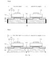
- FIGS. 1 to 11 are sectional views showing a light emitting device and a method of manufacturing the same according to the embodiment
- FIG. 12 is a view showing a light emitting device package including a light emitting device according to embodiments.
- FIG. 13 is a view showing a backlight unit including a light emitting device or a light emitting device package according to the embodiment.
- FIG. 14 is a lighting system including a light emitting device or a light emitting device package according to the embodiment.
- FIGS. 1 to 11 are sectional views showing a light emitting device and a method of manufacturing the same according to the embodiment.
- a light emitting structure layer 135 is formed on a growth substrate 101.
- the light emitting structure layer 135 includes a first conductive semiconductor layer 110, an active layer 120 on the first conductive semiconductor layer 110, and a second conductive semiconductor layer 130 on the active layer 120.
- the growth substrate 101 may include one of sapphire (Al 2 0 3 ), GaN, SiC, ZnO, Si, GaP, InP, or GaAs.
- a buffer layer and/or an undoped semiconductor layer may be formed on the growth substrate 101.
- the light emitting structure layer 135 may include a GaN-based semiconductor layer.
- the light emitting structure layer 135 may include at least one of GaN, InGaN, AlGaN, or InAlGaN.
- the first conductive semiconductor layer 110 may include an N-type semiconductor layer.
- the first conductive semiconductor layer 110 may include a semiconductor material having a composition formula of In x Al y Ga 1-x-y N (0 ⁇ x ⁇ 1, 0 ⁇ y ⁇ 1, 0 ⁇ x+y ⁇ 1).
- the first conductive semiconductor layer 110 may include InAlGaN, GaN, AlGaN, AlInN, InGaN, AIN, or InN.
- the first conductive semiconductor layer 110 may be doped with N-type dopants such as Si, Ge, and Sn.
- the active layer 120 may have one of a single quantum structure, a multi-quantum well structure, a quantum dot structure, and a quantum wire structure, but the embodiment is not limited thereto.
- the active layer 120 may include a semiconductor material having a composition formula of In x Al y Ga 1-x-y N (0 ⁇ x ⁇ 1, 0 ⁇ y ⁇ 1, 0 ⁇ x+y ⁇ 1). If the active layer 120 is formed in the MQW structure, the active layer 120 may have a stack structure of plural well layers and plural barrier layers. For instance, the active layer 120 may have a stack structure of an InGaN well layer/a GaN barrier layer.
- a clad layer (not shown) doped with n-type dopants or p-type dopants may be formed above and/or below the active layer 120, and may include an AlGaN layer or an InAlGaN layer.
- the second conductive semiconductor layer 130 may include a P-type semiconductor layer.
- the second conductive semiconductor layer 130 may include a semiconductor material having a composition formula of In x Al y Ga 1-x-y N (0 ⁇ x ⁇ 1, 0 ⁇ y ⁇ 1, 0 ⁇ x+y ⁇ 1).
- the second conductive semiconductor layer 130 may include InAlGaN, GaN, AlGaN, InGaN, AlInN, AIN, or InN.
- the second conductive semiconductor layer 130 may include P-type dopants such as Mg, Zn, Ca, Sr, and Ba.
- the first conductive semiconductor layer 110 may include a P-type semiconductor layer
- the second conductive semiconductor layer 130 may include an N-type semiconductor layer.
- a third conductive semiconductor layer (not shown) including an N-type semiconductor layer or a P-type semiconductor layer may be formed on the second conductive semiconductor layer 130.
- the light emitting structure layer 135 may have at least one of NP, PN, NPN, or PNP junction structures.
- the doping density of dopants of the first and second conductive semiconductor layers 110 and 130 may be regular or irregular.
- the light emitting structure layer 135 may have various structures, but the embodiment is not limited thereto.
- the light emitting structure layer 135 including the first conductive semiconductor layer 110, the active layer 120, and the second conductive semiconductor layer 130 may have variously modified structures. In other words, the light emitting structure layer 135 is not limited to the above structure according to the embodiment.
- a plurality of light emitting device chips may be provided together.
- first and second chips will be described for the purpose of explanation.
- protective layer 140 is selectively formed on the second conductive semiconductor layer 130.
- the protective layer 140 may be selectively formed on the second conductive semiconductor layer 130 along outer peripheral portions of the first and second chip regions.
- the protective layer 140 may include an insulating material or a material that does not generate fragments in an isolation etching process.
- the protective layer 140 may include at least one of SiO 2 , SiO x , Si x N y , Al 2 O 3 , TiO 2 , ITO, IZO, or AZO.
- the protective layer 140 can prevent the light emitting structure layer 135 from being electrically shorted in the isolation etching process.
- a contact layer 150 is formed on the second conductive semiconductor layer 130.
- the contact layer 150 may be formed on the protective layer 140.
- the contact layer 150 may include at least one of Al, Ag, Pd, Rh, or Pt, or the alloy thereof.
- the contact layer 150 may include a material having an ohmic contact property or high reflection efficiency.
- a conductive support member 160 is formed on the contact layer 150.
- the conductive support member 160 may include at least one of copper (Cu), titanium (Ti), chromium (Cr), nickel (Ni), aluminum (Al), platinum (Pt), gold (Au), molybdenum (Mo), and a carrier wafer including Si, Ge, GaAs, ZnO, SiGe, GaN, or Ga 2 O 3 .
- the conductive support member 160 serves as a base substrate.
- the conductive support member 160 may be formed through a plating process or a bonding process.
- the thickness of the conductive support member 160 may be in the range of about 10 ⁇ m to about 500 ⁇ m.
- the conductive support member 160 supports the light emitting structure layer 135.
- the contact layer 150 and the conductive support member 160 may be formed as one layer.
- the contact layer 150 and the conductive support member 160 may be prepared as a support member having high reflectance, but the embodiment is not limited thereto.
- the growth substrate 101 is removed.
- the growth substrate 101 may be removed through a laser lift off (LLO) scheme or a chemical lift off (CLO) scheme.
- LLO laser lift off
- CLO chemical lift off
- a laser beam having a predetermined wavelength band is irradiated into the growth substrate 101 to separate the growth substrate 101.
- another semiconductor layer e.g., buffer layer
- the CLO scheme may be employed to remove the buffer layer using wet etchant.
- a surface of the first conductive semiconductor layer 110 without the growth substrate 101 may be polished through a polisher.
- FIG. 5 For reference, the structure of FIG. 5 is obtained by reversing the structure of FIG. 4 .
- an isolation etching process is performed with respect to the light emitting structure layer 135 to selectively remove the light emitting structure layer 135, so that a chip boundary region 105 is formed.
- the light emitting structure layer 135 is divided into a plurality of chip units by the chip boundary region 105.
- the light emitting structure layer 135 may be divided into first and second chips.
- the isolation etching process may be performed in the chip boundary region 105 such that the protective layer 140 may be exposed, but the embodiment is not limited thereto.
- an electrode 171 may be formed in a predetermined pattern on the first conductive semiconductor layer 110.
- a first chip protective layer 180 may be formed on the light emitting structure layer 135 and the protective layer 140, and a first support layer 190 may be formed under the conductive support member 160.
- the first chip protective layer 180 prevents the light emitting structure layer 135 from being damaged when the LLO process is performed to form an individual chip.
- the first support layer 190 supports the light emitting structure layer 135 and the conductive support member 160 when the LLO process is performed.
- the first chip protective layer 180 and the first support layer 190 may be omitted or added if necessary.
- a chip protective layer may be additionally interposed between the conductive support member 160 and the first support layer 190.
- the first chip protective layer 180 may include a photoresist layer, but the embodiment is not limited thereto.
- the first support layer 190 may be provided in the form of an adhesive sheet such as a UV sheet or a blue sheet, having an adhesion property, but the embodiment is not limited thereto.
- a laser scribing process is performed along the chip boundary region 105 through the first chip protective layer 180, the protective layer 140, the contact layer 150, and the conductive support member 160, thereby forming a separating section 200 to separate chip regions from each other in a chip unit.
- the separating section 200 may be formed to separate the first and second chips from each other.
- the separating section 200 partially separates the first and second chips from each other.
- the conductive support member 160 is melted during the laser scribing process, the melted conductive support member 160 is cured to form a re-combination section 165 after the laser scribing process has been finished.
- the re-combination section 165 partially connects the conductive support members 160 to each other, and the thickness of the re-combination section 165 is increased as the thickness of the conductive support member 160 is increased.
- the first chip protective layer 180 and the first support layer 190 may be removed after the laser scribing process.
- an etching process is performed with respect to the separating section 200 to remove at least a portion of the re-combination section 165, so that a sub-re-combination section 165a remains as shown in FIG. 9 .
- the etching process may include wet etching employing a chemical solution as etchant, and dry etching employing gas as etchant.
- FIG. 9 shows a case in which the wet etching is used.
- an etch profile of the separating section 200 that is, a lateral surface 168 of the conductive support member 160 becomes a curved surface recessed inward. This is because the wet etching can be performed as isotropic etching having no specific orientation.
- the etch profile that is, the lateral surface 168 of the conductive support member 160 is more recessed as the contact with the etchant is increased.
- the lateral surface 168 of the conductive support member 160 is recessed at an upper portion more than at a lower portion.
- etching can be achieved with a uniform orientation. Accordingly, different from the wet etching, the conductive support member 160 may not have the curved lateral surface 168 recessed inward. However, the dry etching may be slowly performed.
- a second support layer 210 may be formed under the conductive support member 160.
- the second support layer 210 may be provided in the form of an adhesive sheet, such as a UV sheet or a blue sheet, having an adhesion property, but the embodiment is not limited thereto.
- the second support layer 210 fixes the separate portions of the light emitting device such that the separate portions of the light emitting device are not scattered.
- a second protective layer (not shown) is formed on the light emitting structure layer 135 and the electrode 171, thereby protecting the light emitting device in the following breaking process.
- the breaking process is performed with respect to the separating section 200 to separate a plurality of chips from each other in a chip unit. As shown in FIGS. 10 and 11 , the first and second chips are separated from each other through the breaking process.
- the re-combination section 165 of the separating section 200 is cut by using a cutter, so that the first and second chips are completely separated from each other in a chip unit.
- the thickness of the re-combination section 165 becomes increased as the thickness of the conductive support member 160 is increased. Accordingly, if the breaking process is directly performed with respect to the separating section 200 without the etching process according to the embodiment, the probability of the failure of the light emitting device resulting from cracks is increased as the thickness of the re-combination section 165 is increased.
- the yield rate in the manufacturing process of the light emitting device is in the range of about 70% to about 80%. However, if the thickness of the conductive support member 160 exceeds 150 ⁇ m, the yield rate in the manufacturing process of the light emitting device approximates 0%.
- the thickness of the re-combination section 165 is reduced, so that defects caused by the breaking process can be lowered, and the yield rate in the manufacturing process of the light emitting device can be improved.
- the etching process according to the embodiment may be performed when the thickness of the conductive support member 160 is in the range of about 75 ⁇ m to about 500 ⁇ m. Even if the conductive support member 160 has a thick thickness, the yield rate in the manufacturing process of the light emitting device can be improved.
- the thickness of the conductive support member 160 may be in the range of about 75 ⁇ m to about 500 ⁇ m.
- the second support layer 210 and the second chip protective layer may be removed after the breaking process has been performed.
- the light emitting device according to the embodiment can be provided.
- the light emitting device includes the conductive support member 160, the light emitting structure layer 135 on the conductive support member 160, and the electrode 171 on the light emitting structure layer 135.
- a portion of the protective layer 140 may be provided between the conductive support member 160 and the light emitting structure layer 135, and the portion of the protective layer 140 may be exposed upwardly.
- a contact layer 150 may be interposed between the light emitting structure layer 135 and the conductive support member 160, and may be simultaneously interposed between the protective layer 140 and the conductive support member 160.
- the conductive support member 160 may have the curved lateral surface 168 recessed inward.
- the lateral surface 168 of the conductive support member 160 may vertically overlap with the protective layer 140.
- FIG. 12 is a sectional view showing a light emitting device package 600 having the light emitting device according to the embodiments.
- the light emitting device package 600 includes a package body 300, first and second electrode layers 310 and 320 formed on the package body 300, the light emitting device 200 provided on the package body 300 and electrically connected to the first and second electrode layers 31 and 32 and a molding member 500 that surrounds the light emitting device 200.
- the package body 300 may include one of silicon, synthetic resin or metallic material.
- An inclined surface may be formed around the light emitting device 200.
- the first and second electrode layers 310 and 320 are electrically isolated from each other to supply power to the light emitting device 200.
- the first and second electrode layers 310 and 320 reflect the light emitted from the light emitting device 200 to improve the light efficiency and dissipate heat generated from the light emitting device 200 to the outside.
- the light emitting device 200 can be installed on the package body 300 or the first and second electrode layers 310 and 320.
- the light emitting device 200 is electrically connected to the first and second electrode layers 310 and 320 through a wire 400.
- the molding member 500 surrounds the light emitting device 200 to protect the light emitting device 200.
- the molding member 500 may include phosphors to change the wavelength of the light emitted from the light emitting device 200.
- the light emitting device package 600 includes the light emitting device 200 in which the damage of a light emitting structure layer is less, the light emitting device package 600 may represent superior light emission efficiency.
- a plurality of the light emitting device packages 600 according to the embodiment are arrayed on a substrate, and a light guide plate, a prism sheet, a diffusion sheet, and a fluorescent sheet, which are optical members, may be provided on a path of light emitted from the light emitting device package 600.
- the light emitting device package, the substrate, and the optical members constitute a backlight unit or a lighting unit.
- a lighting system may include the backlight unit, the lighting unit, an indicator, a lamp, and a street lamp.
- FIG. 13 is an exploded perspective view showing a backlight unit 1100 including the light emitting device or the light emitting device package according to the embodiment.
- the backlight unit 1100 shown in FIG. 13 is an example of a lighting system, but the embodiment is not limited thereto.
- the backlight unit 1100 includes a bottom frame 1140, a light guide member 1120 installed in the bottom frame 1140, and a light emitting module 1110 installed at one lateral surface or on the bottom surface of the light guide frame 1120.
- a reflective sheet 1130 is disposed under the light guide member 1120
- the bottom frame 1140 has a box shape having a top surface being open to receive the light guide member 1120, the light emitting module 1110 and the reflective sheet 1130 therein.
- the bottom frame may include metallic material or resin material, but the embodiment is not limited thereto.
- the light emitting module 1110 may include a substrate 700 and a plurality of light emitting device packages 600 installed on the substrate 700.
- the light emitting device packages 600 provide the light to the light guide member 1120.
- the light emitting module 1110 includes the light emitting device package 600 provided on the substrate 700, the light emitting device 200 according to the embodiment may be directly installed in the light emitting module 1110.
- the light emitting module 1110 is installed on at least one inner side of the bottom frame 1140 to provide the light to at least one side of the light guide member 1120.
- the light emitting module 1110 can be provided below the bottom frame 1140 to provide the light toward the bottom surface of the light guide member 1120.
- Such an arrangement can be variously changed according to the design of the backlight unit 1100, but the embodiment is not limited thereto.
- the light guide member 1120 may be installed in the bottom frame 1140.
- the light guide member 1120 converts the light emitted from the light emitting module 1110 into the surface light to guide the surface light toward a display panel (not shown).
- the light guide member 1120 may include a light guide plate.
- the light guide plate may include one selected from the group consisting of acryl-based resin, such as PMMA (polymethyl methacrylate), PET (polyethylene terephthalate), PC (polycarbonate), COC or PEN (polyethylene naphthalate) resin.
- PMMA polymethyl methacrylate
- PET polyethylene terephthalate
- PC polycarbonate
- COC polycarbonate
- PEN polyethylene naphthalate
- An optical sheet 1150 may be provided over the light guide member 1120.
- the optical sheet 1150 may include at least one of a diffusion sheet, a light collection sheet, a brightness enhancement sheet, and a fluorescent sheet.
- the optical sheet 1150 may have a stack structure of the diffusion sheet, the light collection sheet, the brightness enhancement sheet, and the fluorescent sheet.
- the diffusion sheet uniformly diffuses the light emitted from the light emitting module 1110 such that the diffused light can be collected on a display panel (not shown) by the light collection sheet.
- the light output from the light collection sheet is randomly polarized and the brightness enhancement sheet increases the degree of polarization of the light output from the light collection sheet.
- the light collection sheet may include a horizontal and/or vertical prism sheet.
- the brightness enhancement sheet may include a dual brightness enhancement film and the fluorescent sheet may include a transmissive plate or a transmissive film including phosphors.
- the reflective sheet 1130 may be disposed below the light guide member 1120.
- the reflective sheet 1130 reflects the light, which is emitted through the bottom surface of the light guide member 1120, toward the light exit surface of the light guide member 1120.
- the reflective sheet 1130 may include resin material having high reflectivity, such as PET, PC or PVC resin, but the embodiment is not limited thereto.
- FIG. 14 is a perspective view showing a lighting unit 1200 including a light emitting device or a light emitting device package according to the embodiment.
- the illumination unit 1200 shown in FIG. 14 is an example of a lighting system, but the embodiment is not limited thereto.
- the lighting unit 1200 includes a case body 1210, a light emitting module 1230 installed in the case body 1210, and a connection terminal 1220 installed in the case body 1210 to receive power from an external power source.
- the case body 1210 includes material having superior heat dissipation property.
- the case body 1210 includes metallic material or resin material.
- the light emitting module 1230 may include a substrate 700 and at least one light emitting device package 600 installed on the substrate 700. According to the embodiment, although the light emitting module 1110 according to the embodiment includes the light emitting device package 600 provided on the substrate 700, the light emitting device 200 may be directly installed in the light emitting module 1110.
- the substrate 700 includes an insulating member printed with a circuit pattern.
- the substrate 300 includes a PCB (printed circuit board), an MC (metal core) PCB, an F (flexible) PCB, or a ceramic PCB.
- the substrate 700 may include material that effectively reflects the light.
- the surface of the substrate 300 can be coated with a color, such as a white color or a silver color, to effectively reflect the light.
- At least one light emitting device package 600 can be installed on the substrate 700.
- Each light emitting device package 600 may include at least one LED (light emitting diode).
- the LED may include a colored LED that emits the light having the color of red, green, blue or white and a UV (ultraviolet) LED that emits UV light.
- the LEDs of the light emitting module 1230 can be variously arranged to provide various colors and brightness.
- the combination of the white LED, the red LED and the green LED can be arranged to achieve the high color rendering index (CRI).
- a fluorescent sheet may further be provided in the path of the light emitted from the light emitting module 1230 to change the wavelength of the light emitted from the light emitting module 1230.
- the fluorescent sheet may include yellow phosphors. In this case, the light emitted from the light emitting module 1230 passes through the fluorescent sheet so that the light is viewed as white light.
- connection terminal 1220 is electrically connected to the light emitting module 1230 to supply power to the light emitting module 1230.
- the connection terminal 1220 has a shape of a socket screw-coupled with the external power source, but the embodiment is not limited thereto.
- the connection terminal 1220 can be prepared in the form of a pin inserted into the external power source or connected to the external power source through a wire.
- At least one of the light guide member, the diffusion sheet, the light collection sheet, the brightness enhancement sheet and the fluorescent sheet is provided in the path of the light emitted from the light emitting module, so that the desired optical effect can be achieved.
- any reference in this specification to "one embodiment,” “an embodiment,” “example embodiment,” etc. means that a particular feature, structure, or characteristic described in connection with the embodiment is included in at least one embodiment of the invention.
- the appearances of such phrases in various places in the specification are not necessarily all referring to the same embodiment.
Landscapes
- Led Devices (AREA)
- Led Device Packages (AREA)
- Non-Portable Lighting Devices Or Systems Thereof (AREA)
Applications Claiming Priority (1)
| Application Number | Priority Date | Filing Date | Title |
|---|---|---|---|
| KR1020090051249A KR100986544B1 (ko) | 2009-06-10 | 2009-06-10 | 반도체 발광소자 및 그 제조방법 |
Publications (2)
| Publication Number | Publication Date |
|---|---|
| EP2262015A2 true EP2262015A2 (de) | 2010-12-15 |
| EP2262015A3 EP2262015A3 (de) | 2012-10-17 |
Family
ID=42646330
Family Applications (1)
| Application Number | Title | Priority Date | Filing Date |
|---|---|---|---|
| EP10165238A Ceased EP2262015A3 (de) | 2009-06-10 | 2010-06-08 | Lichtemittierende Vorrichtung, Verfahren zu deren Herstellung, Verpackung für lichtemittierende Vorrichtung und Beleuchtungssystem |
Country Status (4)
| Country | Link |
|---|---|
| US (2) | US7956379B2 (de) |
| EP (1) | EP2262015A3 (de) |
| KR (1) | KR100986544B1 (de) |
| CN (1) | CN101924174B (de) |
Families Citing this family (6)
| Publication number | Priority date | Publication date | Assignee | Title |
|---|---|---|---|---|
| US8940561B2 (en) * | 2008-01-15 | 2015-01-27 | Cree, Inc. | Systems and methods for application of optical materials to optical elements |
| US8058088B2 (en) | 2008-01-15 | 2011-11-15 | Cree, Inc. | Phosphor coating systems and methods for light emitting structures and packaged light emitting diodes including phosphor coating |
| KR101064026B1 (ko) * | 2009-02-17 | 2011-09-08 | 엘지이노텍 주식회사 | 발광 디바이스 패키지 및 그 제조방법 |
| KR20120075946A (ko) * | 2010-12-29 | 2012-07-09 | 서울반도체 주식회사 | 전원공급소자 통합형 웨이퍼를 갖는 발광모듈 |
| US9508904B2 (en) * | 2011-01-31 | 2016-11-29 | Cree, Inc. | Structures and substrates for mounting optical elements and methods and devices for providing the same background |
| US9166126B2 (en) | 2011-01-31 | 2015-10-20 | Cree, Inc. | Conformally coated light emitting devices and methods for providing the same |
Citations (1)
| Publication number | Priority date | Publication date | Assignee | Title |
|---|---|---|---|---|
| US20030141506A1 (en) * | 2002-01-28 | 2003-07-31 | Masahiko Sano | Nitride semiconductor element with a supporting substrate and a method for producing a nitride semiconductor element |
Family Cites Families (12)
| Publication number | Priority date | Publication date | Assignee | Title |
|---|---|---|---|---|
| US20030189215A1 (en) * | 2002-04-09 | 2003-10-09 | Jong-Lam Lee | Method of fabricating vertical structure leds |
| US8294172B2 (en) * | 2002-04-09 | 2012-10-23 | Lg Electronics Inc. | Method of fabricating vertical devices using a metal support film |
| US7244628B2 (en) * | 2003-05-22 | 2007-07-17 | Matsushita Electric Industrial Co., Ltd. | Method for fabricating semiconductor devices |
| SG153627A1 (en) * | 2003-10-31 | 2009-07-29 | Micron Technology Inc | Reduced footprint packaged microelectronic components and methods for manufacturing such microelectronic components |
| US7626211B2 (en) * | 2004-09-16 | 2009-12-01 | Hitachi Aic Inc. | LED reflecting plate and LED device |
| JP4841909B2 (ja) | 2005-09-14 | 2011-12-21 | 昭和電工株式会社 | 窒化物系半導体発光素子 |
| KR20070044099A (ko) * | 2005-10-24 | 2007-04-27 | 김성진 | 질화물 반도체 발광 다이오드 및 그 제조방법 |
| JP5189734B2 (ja) * | 2006-01-24 | 2013-04-24 | ローム株式会社 | 窒化物半導体発光素子 |
| KR100774196B1 (ko) * | 2006-03-14 | 2007-11-08 | 엘지전자 주식회사 | 수직형 발광 소자 제조방법 |
| KR100854328B1 (ko) * | 2006-07-07 | 2008-08-28 | 엘지전자 주식회사 | 발광 소자 패키지 및 그 제조방법 |
| TWI320237B (en) * | 2006-07-24 | 2010-02-01 | Si-substrate and structure of opto-electronic package having the same | |
| KR100887479B1 (ko) * | 2007-10-09 | 2009-03-10 | 주식회사 네패스 | 내균열성 반도체 패키지 및 그 제조 방법 |
-
2009
- 2009-06-10 KR KR1020090051249A patent/KR100986544B1/ko not_active Expired - Fee Related
-
2010
- 2010-06-08 EP EP10165238A patent/EP2262015A3/de not_active Ceased
- 2010-06-09 US US12/796,780 patent/US7956379B2/en active Active
- 2010-06-10 CN CN201010206491.7A patent/CN101924174B/zh active Active
-
2011
- 2011-04-27 US US13/095,173 patent/US8486732B2/en active Active
Patent Citations (1)
| Publication number | Priority date | Publication date | Assignee | Title |
|---|---|---|---|---|
| US20030141506A1 (en) * | 2002-01-28 | 2003-07-31 | Masahiko Sano | Nitride semiconductor element with a supporting substrate and a method for producing a nitride semiconductor element |
Also Published As
| Publication number | Publication date |
|---|---|
| KR100986544B1 (ko) | 2010-10-07 |
| CN101924174B (zh) | 2015-04-01 |
| CN101924174A (zh) | 2010-12-22 |
| US20100314656A1 (en) | 2010-12-16 |
| EP2262015A3 (de) | 2012-10-17 |
| US20110201140A1 (en) | 2011-08-18 |
| US7956379B2 (en) | 2011-06-07 |
| US8486732B2 (en) | 2013-07-16 |
Similar Documents
| Publication | Publication Date | Title |
|---|---|---|
| EP2355193B1 (de) | Leuchtdiode und Gehäuse mit dem gleichen | |
| EP2365538B1 (de) | Leuchtdiode und Herstellungsverfahren dafür | |
| EP2312631B1 (de) | Lichtemittierende Vorrichtung und lichtemittierendes Vorrichtungspaket damit | |
| US20110193058A1 (en) | Light emitting device and light emitting device package having the same | |
| US9484496B2 (en) | Light emitting device, method of manufacturing the same, light emitting device package and lighting system | |
| EP2383802B1 (de) | Lichtemittierende Vorrichtung, Herstellungsverfahren für die lichtemittierende Vorrichtung, Gehäuse für lichtemittierende Vorrichtung | |
| US8143639B2 (en) | Light emitting device and light emitting device package having the same | |
| EP2346099B1 (de) | Lichtemittierende Vorrichtung | |
| EP2330643B1 (de) | Lichtemittierende Vorrichtung | |
| US8486732B2 (en) | Method of manufacturing semiconductor light emitting device including step of performing etching process with respect to conductive support member | |
| KR101786082B1 (ko) | 발광 소자 | |
| EP2562828B1 (de) | Leuchtdiode und gehäuse für eine leuchtdiode | |
| US20110089435A1 (en) | Light emitting device, method of manufacturing the same, light emitting device package, and lighting system | |
| KR101830950B1 (ko) | 발광소자 | |
| KR20110118333A (ko) | 발광 소자, 발광 소자 제조방법, 발광 소자 패키지, 및 조명 시스템 | |
| KR20120000974A (ko) | 발광 소자, 발광 소자 제조방법, 발광 소자 패키지 및 조명 시스템 | |
| KR20120045635A (ko) | 발광 소자, 발광 소자 제조방법, 발광 소자 패키지 및 조명 시스템 | |
| KR20120042516A (ko) | 발광 소자, 발광 소자 제조방법, 발광 소자 패키지 및 조명 시스템 | |
| KR20120045636A (ko) | 발광 소자, 발광 소자 제조방법, 발광 소자 패키지 및 조명 시스템 |
Legal Events
| Date | Code | Title | Description |
|---|---|---|---|
| PUAI | Public reference made under article 153(3) epc to a published international application that has entered the european phase |
Free format text: ORIGINAL CODE: 0009012 |
|
| 17P | Request for examination filed |
Effective date: 20100608 |
|
| AK | Designated contracting states |
Kind code of ref document: A2 Designated state(s): AL AT BE BG CH CY CZ DE DK EE ES FI FR GB GR HR HU IE IS IT LI LT LU LV MC MK MT NL NO PL PT RO SE SI SK SM TR |
|
| AX | Request for extension of the european patent |
Extension state: BA ME RS |
|
| RIC1 | Information provided on ipc code assigned before grant |
Ipc: H01L 33/00 20100101AFI20120424BHEP |
|
| PUAL | Search report despatched |
Free format text: ORIGINAL CODE: 0009013 |
|
| AK | Designated contracting states |
Kind code of ref document: A3 Designated state(s): AL AT BE BG CH CY CZ DE DK EE ES FI FR GB GR HR HU IE IS IT LI LT LU LV MC MK MT NL NO PL PT RO SE SI SK SM TR |
|
| AX | Request for extension of the european patent |
Extension state: BA ME RS |
|
| RIC1 | Information provided on ipc code assigned before grant |
Ipc: H01L 33/00 20100101AFI20120913BHEP |
|
| 17Q | First examination report despatched |
Effective date: 20130905 |
|
| RAP1 | Party data changed (applicant data changed or rights of an application transferred) |
Owner name: LG INNOTEK CO., LTD. |
|
| STAA | Information on the status of an ep patent application or granted ep patent |
Free format text: STATUS: THE APPLICATION HAS BEEN REFUSED |
|
| 18R | Application refused |
Effective date: 20151118 |