EP2261995A1 - Solar cell and method for manufacturing the same - Google Patents
Solar cell and method for manufacturing the same Download PDFInfo
- Publication number
- EP2261995A1 EP2261995A1 EP09721439A EP09721439A EP2261995A1 EP 2261995 A1 EP2261995 A1 EP 2261995A1 EP 09721439 A EP09721439 A EP 09721439A EP 09721439 A EP09721439 A EP 09721439A EP 2261995 A1 EP2261995 A1 EP 2261995A1
- Authority
- EP
- European Patent Office
- Prior art keywords
- transparent conductive
- conductive film
- type semiconductor
- semiconductor layer
- solar cell
- Prior art date
- Legal status (The legal status is an assumption and is not a legal conclusion. Google has not performed a legal analysis and makes no representation as to the accuracy of the status listed.)
- Granted
Links
Images

Classifications
-
- H—ELECTRICITY
- H10—SEMICONDUCTOR DEVICES; ELECTRIC SOLID-STATE DEVICES NOT OTHERWISE PROVIDED FOR
- H10F—INORGANIC SEMICONDUCTOR DEVICES SENSITIVE TO INFRARED RADIATION, LIGHT, ELECTROMAGNETIC RADIATION OF SHORTER WAVELENGTH OR CORPUSCULAR RADIATION
- H10F10/00—Individual photovoltaic cells, e.g. solar cells
- H10F10/10—Individual photovoltaic cells, e.g. solar cells having potential barriers
- H10F10/16—Photovoltaic cells having only PN heterojunction potential barriers
- H10F10/164—Photovoltaic cells having only PN heterojunction potential barriers comprising heterojunctions with Group IV materials, e.g. ITO/Si or GaAs/SiGe photovoltaic cells
- H10F10/165—Photovoltaic cells having only PN heterojunction potential barriers comprising heterojunctions with Group IV materials, e.g. ITO/Si or GaAs/SiGe photovoltaic cells the heterojunctions being Group IV-IV heterojunctions, e.g. Si/Ge, SiGe/Si or Si/SiC photovoltaic cells
- H10F10/166—Photovoltaic cells having only PN heterojunction potential barriers comprising heterojunctions with Group IV materials, e.g. ITO/Si or GaAs/SiGe photovoltaic cells the heterojunctions being Group IV-IV heterojunctions, e.g. Si/Ge, SiGe/Si or Si/SiC photovoltaic cells the Group IV-IV heterojunctions being heterojunctions of crystalline and amorphous materials, e.g. silicon heterojunction [SHJ] photovoltaic cells
-
- H—ELECTRICITY
- H10—SEMICONDUCTOR DEVICES; ELECTRIC SOLID-STATE DEVICES NOT OTHERWISE PROVIDED FOR
- H10F—INORGANIC SEMICONDUCTOR DEVICES SENSITIVE TO INFRARED RADIATION, LIGHT, ELECTROMAGNETIC RADIATION OF SHORTER WAVELENGTH OR CORPUSCULAR RADIATION
- H10F10/00—Individual photovoltaic cells, e.g. solar cells
- H10F10/10—Individual photovoltaic cells, e.g. solar cells having potential barriers
- H10F10/17—Photovoltaic cells having only PIN junction potential barriers
-
- H—ELECTRICITY
- H10—SEMICONDUCTOR DEVICES; ELECTRIC SOLID-STATE DEVICES NOT OTHERWISE PROVIDED FOR
- H10F—INORGANIC SEMICONDUCTOR DEVICES SENSITIVE TO INFRARED RADIATION, LIGHT, ELECTROMAGNETIC RADIATION OF SHORTER WAVELENGTH OR CORPUSCULAR RADIATION
- H10F71/00—Manufacture or treatment of devices covered by this subclass
- H10F71/138—Manufacture of transparent electrodes, e.g. transparent conductive oxides [TCO] or indium tin oxide [ITO] electrodes
-
- H—ELECTRICITY
- H10—SEMICONDUCTOR DEVICES; ELECTRIC SOLID-STATE DEVICES NOT OTHERWISE PROVIDED FOR
- H10F—INORGANIC SEMICONDUCTOR DEVICES SENSITIVE TO INFRARED RADIATION, LIGHT, ELECTROMAGNETIC RADIATION OF SHORTER WAVELENGTH OR CORPUSCULAR RADIATION
- H10F77/00—Constructional details of devices covered by this subclass
- H10F77/20—Electrodes
- H10F77/244—Electrodes made of transparent conductive layers, e.g. transparent conductive oxide [TCO] layers
- H10F77/247—Electrodes made of transparent conductive layers, e.g. transparent conductive oxide [TCO] layers comprising indium tin oxide [ITO]
-
- H—ELECTRICITY
- H10—SEMICONDUCTOR DEVICES; ELECTRIC SOLID-STATE DEVICES NOT OTHERWISE PROVIDED FOR
- H10F—INORGANIC SEMICONDUCTOR DEVICES SENSITIVE TO INFRARED RADIATION, LIGHT, ELECTROMAGNETIC RADIATION OF SHORTER WAVELENGTH OR CORPUSCULAR RADIATION
- H10F77/00—Constructional details of devices covered by this subclass
- H10F77/20—Electrodes
- H10F77/244—Electrodes made of transparent conductive layers, e.g. transparent conductive oxide [TCO] layers
- H10F77/251—Electrodes made of transparent conductive layers, e.g. transparent conductive oxide [TCO] layers comprising zinc oxide [ZnO]
-
- Y—GENERAL TAGGING OF NEW TECHNOLOGICAL DEVELOPMENTS; GENERAL TAGGING OF CROSS-SECTIONAL TECHNOLOGIES SPANNING OVER SEVERAL SECTIONS OF THE IPC; TECHNICAL SUBJECTS COVERED BY FORMER USPC CROSS-REFERENCE ART COLLECTIONS [XRACs] AND DIGESTS
- Y02—TECHNOLOGIES OR APPLICATIONS FOR MITIGATION OR ADAPTATION AGAINST CLIMATE CHANGE
- Y02E—REDUCTION OF GREENHOUSE GAS [GHG] EMISSIONS, RELATED TO ENERGY GENERATION, TRANSMISSION OR DISTRIBUTION
- Y02E10/00—Energy generation through renewable energy sources
- Y02E10/50—Photovoltaic [PV] energy
- Y02E10/548—Amorphous silicon PV cells
Definitions
- the present invention relates to a solar cell including transparent conductive films formed on a photoelectric conversion body and a method for manufacturing the same.
- Solar cells are expected as a new source of energy, because solar cells are capable of directly converting light, which comes from the sun as a clean, unlimited source of energy, to electricity.
- a solar cell includes a photoelectric conversion body which has an n-type semiconductor layer and a p-type semiconductor layer and receives light to generate photogenerated carriers.
- the carriers are extracted from the photoelectric conversion body through electrodes formed on the n- and p-type semiconductor layers.
- Each electrode to be used has a layered structure of a transparent conductive film and a metallic layer in some cases. In such a case, it is desirable that the transparent conductive film have low electric resistivity.
- the surface characteristics of the photoelectric conversion body could be degraded. Specifically, hydrogen radicals having reducing properties could degrade the surfaces of the n- and p-type semiconductor layers when the transparent conductive films are formed.
- the present invention was made in the light of the aforementioned problem, and an object of the present invention is to provide a solar cell with the surface characteristics of the photoelectric conversion body prevented from being degraded and a method for manufacturing the same.
- the solar cell is summarized as comprising a photoelectric conversion body configured to generate photogenerated carriers upon receiving light; a first transparent conductive film formed on a first major surface of the photoelectric conversion body; and a second transparent conductive film formed on a second major surface provided on an side opposite to the first major surface, wherein the first major surface is formed by an n-type semiconductor layer, the second major surface is formed by a p-type semiconductor layer, and a hydrogen atom content of a part of the first transparent conductive film on a side close to the n-type semiconductor layer is lower than a hydrogen atom content of the second transparent conductive film.
- the hydrogen atom content of the first transparent conductive film formed on the first major surface on the n-type semiconductor layer side is lower than that of the second transparent conductive film formed on the second major surface. This can reduce the effect of hydrogen radicals on the surface of the n-type semiconductor layer forming the first major surface of the photoelectric conversion body. The degradation of the surface characteristics of the photoelectric conversion body can be therefore prevented.
- the hydrogen atom content of a part of the first transparent conductive film on an side opposite to the n-type semiconductor layer may be higher than the hydrogen atom content of the part of the first transparent conductive film on the side close to the n-type semiconductor layer.
- the part of the first transparent conductive film on the side close to the n-type semiconductor layer may be made of a different material from a material of the part of the first transparent conductive film on the side opposite to the n-type semiconductor layer.
- the photoelectric conversion body is mainly made of single-crystalline silicon and each of the n-type semiconductor layer and the p-type semiconductor layer is mainly made of an amorphous silicon semiconductor.
- the method for manufacturing a solar cell is summarized as including a photoelectric conversion body configured to generate photogenerated carriers upon receiving light, the method comprising: a step A of forming a first transparent conductive film in an atmosphere not containing hydrogen on a first major surface of the photoelectric conversion body; and a step B of forming a second transparent conductive film in an atmosphere containing hydrogen on a second major surface provided on an side opposite to the first major surface, wherein the first major surface is formed by an n-type semiconductor layer, the second major surface is formed by a p-type semiconductor layer, and in the step B, the second transparent conductive film is formed while hydrogen atoms are being supplied.
- the step B may be performed after the step A is performed.
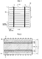
- Fig. 1 is a plan view of the solar cell 10 on a second major surface S2 side.
- Fig. 2 is an A-A cross-sectional view of Fig. 1 .
- the solar cell 10 includes a solar cell substrate 1, fine-line electrodes 2, and connecting electrodes 3.
- the solar cell substrate 1 includes a photoelectric conversion body 11, a first transparent conductive film 12, and a second transparent conductive film 13.
- the photoelectric conversion body 11 is configured to generate photogenerated carriers upon receiving light.
- the solar cell substrate 1 includes a first major surface S1 (the lower surface in Fig. 2 ) and a second major surface S2 (the upper surface in Fig. 2 ) provided on the opposite side to the first major surface S1. The structure of the solar cell substrate 1 is described later.
- the fine-line electrodes 2 are collecting electrodes configured to collect photogenerated carriers from the photoelectric conversion body 11.
- the fine-line electrodes 2 are formed on the second major surface S2 of the solar cell substrate 1 along a first direction substantially parallel to a side of the solar cell substrate 1 as shown in Fig. 1 . Some of the plurality of fine-line electrodes 2 are arranged substantially at regular intervals in a second direction substantially orthogonal to the first direction.
- the other fine-line electrodes 2 (not shown) are formed on the first major surface S1 of the solar cell substrate 1 in a similar manner to those on the second major surface S2 of the solar cell substrate 1.
- the fine-line electrodes 2 formed on the second major surface S2 of the solar cell substrate 1 collect carriers from the photoelectric conversion body 11 through the second transparent conductive film 13 later described.
- the fine-line electrodes 2 formed on the first major surface S1 of the solar cell substrate 1 collect carriers from the photoelectric conversion body 11 through the first transparent conductive film 12 later described.
- the fine-line electrodes 2 can be formed, for example, by printing resin-type conductive paste which includes a resin material as a binder and conductive particles such as silver particles as a filler or sintered-type conductive paste containing silver powder, glass frit, organic vehicle, organic solvent, and the like (so-called ceramic paste) by using a printing process.
- resin-type conductive paste which includes a resin material as a binder and conductive particles such as silver particles as a filler or sintered-type conductive paste containing silver powder, glass frit, organic vehicle, organic solvent, and the like (so-called ceramic paste) by using a printing process.
- Each fine-line electrode 2 may be formed as a metallic film by deposition.
- the number and size of the fine-line electrodes 2 can be set to proper values in consideration of the size of the photoelectric conversion body 11 and the like.
- the connecting electrodes 3 are electrodes connected to wiring materials (not shown) electrically connecting a plurality of the solar cells 10 in series or in parallel.
- the connecting electrodes 3 are formed on the second major surface S2 of the solar cell substrate 1 along the second direction as shown in Fig. 1 . Accordingly, some of the connecting electrodes 3 intersect the plurality of fine-line electrodes 2 and are electrically connected to the plurality of fine-line electrodes 2.
- the other connecting electrodes 3 (not shown) are formed on the first major surface S1 of the solar cell substrate 1 in a similar manner to the first major surface S2 of the solar cell substrate 1.
- the connecting electrodes 3 can be formed by printing or deposition in a similar way to the fine-line electrodes 2.
- the number and size of the connecting electrodes 3 can be set to proper values in consideration of the size of the photoelectric conversion body 11 and the like.
- the solar cell substrate 1 includes the photoelectric conversion body 11 and the first and second transparent conductive films 12 and 13 as shown in Fig. 2 .
- the photoelectric conversion body 11 includes the first major surface S1 (the lower surface in Fig. 2 ) and the second major surface S2 (the upper surface in Fig. 2 ) provided on the opposite side to the first major surface S1.
- the photoelectric conversion body 11 receives light through the first or second major surface S1 or S2 of the photoelectric conversion body 11 to generate photogenerated carriers.
- Each of the photogenerated carriers refers to a pair of a hole and an electron generated upon the photoelectric conversion body 11 absorbing solar light.
- the photoelectric conversion body 11 includes an n-type substrate 11a, an i-type semiconductor layer 11b, a p-type semiconductor layer 11c, an i-type semiconductor layer 11d, and an n-type semiconductor layer 11e as shown in Fig. 2 .
- the n-type substrate 11a is a main body of the photoelectric conversion body 11.
- an n-type single-crystalline silicon substrate can be used, for example.
- the p-type semiconductor layer 11e is formed on the second major surface S2 side of the n-type substrate 11a with the i-type semiconductor layer 11b interposed therebetween.
- the n-type semiconductor layer 11e is formed on the first major surface S1 side of the n-type substrate 11a with the i-type semiconductor layer 11d interposed therebetween.
- the second major surface S2 of the photoelectric conversion body 11 is formed by the p-type semiconductor layer 11c
- the first major surface S1 of the photoelectric conversion body 11 is formed by the n-type semiconductor layer 11e.
- the i-type semiconductor layer 11b, p-type semiconductor layer 11c, i-type semiconductor layer 11d, and n-type semiconductor layer 11e for example, an i-type amorphous semiconductor layer, a p-type amorphous semiconductor layer, an i-type amorphous semiconductor layer, and a n-type amorphous semiconductor layer can be used, respectively.
- the i-type semiconductor layers 11b and 11d constituted by i-type amorphous semiconductor layers have such thicknesses that the i-type semiconductor layers 11b and 11d substantially do not contribute to power generation.
- the thicknesses of the i-type semiconductor layers 11b and 11d are preferably in a range from several ⁇ to 250 ⁇ .
- the amorphous semiconductors can be silicon-based semiconductors such as amorphous silicon, amorphous silicon carbide, amorphous silicon germanium, and microcrystalline silicon.
- the structure of the photoelectric conversion body 11 is not limited to the aforementioned structure.
- the photoelectric conversion body 11 does not need to include the i-type semiconductor layers 11b and 11d and may have another structure.
- the first transparent conductive film 12 is formed on the n-type semiconductor layer 11e forming the first major surface S1 of the photoelectric conversion body 11.
- the first transparent conductive film 12 has translucency and conductivity.
- a metal oxide such as indium oxide (In 2 O 3 ), zinc oxide (ZnO), tin oxide (SnO 2 ), or titanium oxide (TiO 2 ) can be used.
- These metal oxides may be doped with a dopant such as tin (Sn), zinc (Zn), tungsten (W), antimony (Sb), titanium (Ti), cerium (Ce), zirconium (Zr), molybdenum (Mo), aluminum (Al), or gallium (Ga).
- a dopant such as tin (Sn), zinc (Zn), tungsten (W), antimony (Sb), titanium (Ti), cerium (Ce), zirconium (Zr), molybdenum (Mo), aluminum (Al), or gallium (Ga).
- concentration of the dopant can be 0 to 20 wt%.
- the second transparent conductive film 13 is formed on the p-type semiconductor layer 11c forming the second major surface S2 of the photoelectric conversion body 11.
- the second transparent conductive film 13 has translucency and conductivity.
- a metal oxide such as indium oxide (In 2 O 3 ), zinc oxide (ZnO), tin oxide (SnO 2 ), or titanium oxide (TiO 2 ) can be used.
- These metal oxides may be doped with a dopant such as tin (Sn), zinc (Zn), tungsten (W), antimony (Sb), titanium (Ti), cerium (Ce), zirconium (Zr), molybdenum (Mo), aluminum (Al), or gallium (Ga).
- a dopant such as tin (Sn), zinc (Zn), tungsten (W), antimony (Sb), titanium (Ti), cerium (Ce), zirconium (Zr), molybdenum (Mo), aluminum (Al), or gallium (Ga).
- the concentration of the dopant can be 0 to 20 wt%.
- the materials constituting the second transparent conductive film 13 may be either the same as or different from materials constituting the first transparent conductive film 12.
- the hydrogen atom content of the first transparent conductive film 12 is lower than that of the second transparent conductive film 13. Accordingly, a metal oxide formed in an atmosphere not containing hydrogen can be used for the first transparent conductive film 12 while a metal oxide formed in an atmosphere supplying hydrogen atoms (an atmosphere containing hydrogen) can be used for the second transparent conductive film 13.
- the n-type substrate 11a is etched to form fine roughness on the first and second major surfaces S1 and S2 sides.
- the i-type and p-type semiconductor layers 11b and 11c are sequentially stacked on the second major surface S2 side of the n-type substrate 11a using CVD or the like.
- the i-type and n-type semiconductor layers 11d and 11e are sequentially stacked on the first major surface S1 side of the n-type substrate 11a in a similar manner.
- the photoelectric conversion body 11 is thus formed.
- the first transparent conductive film 12 is formed on the n-type semiconductor layer 11e by using a sputtering method or the like in an atmosphere not containing hydrogen such as an Ar and O 2 atmosphere.
- the atmosphere not containing hydrogen refers to an atmosphere not actively supplying hydrogen atoms.
- the hydrogen atom contents of the transparent conductive films formed in the atmosphere not containing hydrogen are about 1.0 ⁇ 10 20 to 5.2 ⁇ 10 20 (atoms/cc).
- the second transparent conductive film 13 is formed on the p-type semiconductor layer 11c in an atmosphere containing hydrogen.
- the second transparent conductive film 13 is formed in an Ar, O 2 , and H 2 O atmosphere, an Ar, O 2 , and H 2 atmosphere, or the like where hydrogen atoms are being supplied thereto.
- the hydrogen atom content of the second transparent conductive film 13 is therefore higher than that of the first transparent conductive film 12.
- the solar cell substrate 1 is thus formed.
- the process to form the second transparent conductive film 13 is performed after the process to form the first transparent conductive film 12 is performed.
- epoxy-based thermosetting-type silver paste is placed on the second major surface S2 of the solar cell substrate 1 in a predetermined pattern by using a printing process such as screen printing or off-set printing.
- epoxy-based thermosetting-type silver paste is placed on the first major surface S1 of the solar cell 1 in a predetermined pattern.
- the silver paste is heated under predetermined conditions for volatilization of the solvent and is then further heated for final drying.
- the predetermined patterns have the shapes corresponding to the fine-line electrodes 2 extending along the first direction and the connecting electrodes 3 extending along the second direction as shown in Fig. 1 .
- the solar cell 10 is thus manufactured.
- the first transparent conductive film 12 is formed on the n-type semiconductor layer 11e, which forms the first major surface S1 of the photoelectric conversion body 11, in the atmosphere not containing hydrogen.
- the second transparent conductive film 13 is formed on the p-type semiconductor layer 11c, which forms the second major surface S2 of the photoelectric conversion body 11, in the atmosphere containing hydrogen.
- the hydrogen atom content of the first transparent conductive film 12 formed on the first major surface S1 of the photoelectric conversion body 11 is therefore lower than that of the second transparent conductive film 13 formed on the second major surface S2 of the photoelectric conversion body 11.
- the applicant examined the influence of hydrogen radicals on the surfaces of the p-type and n-type semiconductor layer 11c and 11e in the case where the transparent conductive films were formed in the atmosphere containing hydrogen on the p-type semiconductor layer 11c forming the second major surface S2 of the photoelectric conversion body 11 and on the n-type semiconductor layer 11e forming the first major surface S1 of the photoelectric conversion body 11.
- the applicant found that the surface of the n-type semiconductor layer 11e was more likely to be degraded by hydrogen radicals.
- the first transparent conductive film 12 is formed in the atmosphere not containing hydrogen on the n-type semiconductor layer 11e, the surface of which is more likely to be degraded in the atmosphere containing hydrogen, so that the surface of the n-type semiconductor layer 11e can be prevented from being degraded by hydrogen radicals.
- the second transparent conductive film 13 is formed on the p-type semiconductor layer 11c, which is less affected by hydrogen radicals in the atmosphere containing hydrogen than the n-type semiconductor layer 11e, with hydrogen atoms being actively introduced thereto. This can provide increased translucency and reduced electric resistivity to the second transparent conductive film 13. As described above, in the solar cell 10 according to the first embodiment of the present invention, it is possible to prevent the degradation of the surface characteristics of the photoelectric conversion body 11.
- the second transparent conductive film 13 is formed on the p-type semiconductor layer 11c after the first transparent conductive film 12 is formed on the n-type semiconductor layer 11e, the surface of the n-type semiconductor layer 11e is protected by the first transparent conductive film 12. This can further reduce the influence of hydrogen radicals on the surface of the n-type semiconductor layer 11e when the second transparent conductive film 13 is formed in the atmosphere containing hydrogen.
- the hydrogen atom content of the first transparent conductive film 12 on the n-type semiconductor layer 11e side is substantially the same as that of the first transparent conductive film 12 on the opposite side to the n-type semiconductor layer 11e.
- the hydrogen atom content of the first transparent conductive film 12 on the n-type semiconductor layer 11e side is different from that of the first transparent conductive film 12 on the opposite side to the n-type semiconductor layer 11e.
- the schematic structure of the solar cell 10 according to the second embodiment of the present invention is substantially the same as that of the solar cell 10 according to the first embodiment, and the description thereof is omitted herein.
- the solar cell substrate 1 includes the photoelectric conversion body 11, the first transparent conductive film 12, and the second transparent conductive film 13 as shown in Fig. 3 .
- the structures of the photoelectric conversion body 11 and second transparent conductive film 13 are substantially the same as those of the aforementioned first embodiment, and the description thereof is omitted.
- the first transparent conductive film 12 includes a third transparent conductive film 12a and a fourth transparent conductive film 12b as shown in Fig. 3 .
- the third transparent conductive film 12a is formed on the n-type semiconductor layer 11e forming the first major surface S1 of the photoelectric conversion body 11.
- the fourth transparent conductive film 12b is formed on the third transparent conductive film 12a.
- the third and fourth transparent conductive films 12a and 12b include translucency and conductivity.
- a metal oxide such as indium oxide (In 2 O 3 ), zinc oxide (ZnO), tin oxide (SnO 2 ), or titanium oxide (TiO 2 ) can be used.
- These metal oxides may be doped with a dopant such as tin (Sn), zinc (Zn), tungsten (W), antimony (Sb), titanium (Ti), cerium (Ce), zirconium (Zr), molybdenum (Mo), aluminum (Al), or gallium (Ga).
- a dopant such as tin (Sn), zinc (Zn), tungsten (W), antimony (Sb), titanium (Ti), cerium (Ce), zirconium (Zr), molybdenum (Mo), aluminum (Al), or gallium (Ga).
- concentration of the dopant can be 0 to 20 wt%.
- the hydrogen atom content of the fourth transparent conductive film 12b is higher than that of the third transparent conductive film 12a.
- the hydrogen atom content of a half of the first transparent conductive film 12 on the opposite side to the n-type semiconductor layer 11e is higher than that of the other half on the n-type semiconductor layer 11e side.
- the hydrogen atom content of the third transparent conductive film 12a is lower than that of the second transparent conductive film 13.
- the hydrogen atom content of the half of the first transparent conductive film 12 on the n-type semiconductor layer 11e side is lower than that of the second transparent conductive film 13.
- the third transparent conductive film 12a a metallic oxide formed in the atmosphere not containing hydrogen can be used while a metallic oxide formed in the atmosphere supplying hydrogen atoms (the atmosphere containing hydrogen) in a similar manner to the second transparent conductive film 13 can be used for the fourth transparent conductive film 12b.
- the materials constituting the second, third, and fourth transparent conductive films 13, 12a, and 12b may be the same or different.
- the photoelectric conversion body 11 is formed in the same way as the aforementioned first embodiment.
- the third transparent conductive film 12a is formed on the n-type semiconductor layer 11e, which forms the first major surface S1 of the photoelectric conversion body 11, by using a sputtering method or the like in the atmosphere not containing hydrogen such as an Ar and O 2 atmosphere.
- the second transparent conductive film 13 is formed on the p-type semiconductor layer 11c by using a sputtering method or the like in the atmosphere containing hydrogen. Specifically, the second transparent conductive film 13 is formed in an Ar, O 2 , and water vapor atmosphere, an Ar, O 2 , and hydrogen atmosphere, or the like where hydrogen atoms are being supplied. The hydrogen atom content of the second transparent conductive film 13 is therefore made higher than that of the third transparent conductive film 12a.
- the fourth transparent conductive film 12b is formed on the third transparent conductive film 12a by using a sputtering method or the like in the atmosphere containing hydrogen. Specifically, the fourth transparent conductive film 12b is formed in an Ar, O 2 , and water vapor atmosphere, an Ar, O 2 , and hydrogen atmosphere, or the like where hydrogen atoms are being supplied. The hydrogen atom content of the fourth transparent conductive film 12b is therefore made higher than that of the third transparent conductive film 12a. The first transparent conductive film 12 is thus formed.
- the solar cell substrate 1 is formed in such a manner.
- the fine-line electrodes 2 and connecting electrodes 3 are formed in the same way as the aforementioned first embodiment.
- the solar cell 10 is thus formed.
- the first transparent conductive film 12 formed on the n-type semiconductor layer 11e includes the third and fourth transparent conductive films 12a and 12b.
- the third transparent conductive film 12a is formed on the n-type semiconductor layer 11e in the atmosphere not containing hydrogen
- the fourth transparent conductive film 12b is formed on the third transparent conductive film 12a in the atmosphere containing hydrogen.
- Fig. 4 is a cross-sectional view of a thin film-type solar cell 20.
- the thin film-type solar cell 20 includes a substrate 21 having translucency, a fifth transparent conductive film 22, a photoelectric conversion body 23 configured to receive light and generate photogenerated carriers, a sixth transparent conductive film 24, and a rear electrode layer 25.
- the photoelectric conversion body 23 has a structure in which a p-type semiconductor layer 23a, an i-type semiconductor layer 23b, and an n-type semiconductor layer 23c are sequentially stacked from the substrate 21 side.
- the fifth transparent conductive film 22 is formed on the ) substrate 21 in the atmosphere containing hydrogen
- the sixth transparent conductive film 24 is formed on the n-type semiconductor layer 23c in the atmosphere not containing hydrogen. This can prevent degradation of the surface of the n-type semiconductor layer 23c (corresponding to "the second surface S2" of the aforementioned embodiments).
- the translucency of the fifth transparent conductive film 22 can be increased, and the electrical resistivity thereof can be reduced.
- the structure of the solar cell 20 is not limited to the structure shown in Fig. 4 and may be a structure in which the fifth transparent conductive film 22, photoelectric conversion body 23, sixth transparent conductive film 24, rear electrode layer 25, and substrate 21 are stacked in this order.
- the structure of the photoelectric conversion body 23 is not limited to the structure shown in Fig.
- n-type, i-type, and p-type semiconductor layers 23c, 23b, and 23a are sequentially stacked from the substrate 21 side or a structure in which the p-type and n-type semiconductor layers 23a and 23c are sequentially stacked from the substrate 21 side.
- p-type, i-type, and n-type semiconductor layers 23a, 23b, and 23c p-type, i-type, and n-type semiconductor materials of amorphous Si, amorphous SiC, amorphous SiGe, microcrystalline Si, or the like can be used, respectively.
- the aforementioned first and second embodiments describe about the case where the fine-line electrodes 2 and connecting electrodes 3 having the same shapes as those formed on the second major surface S2 of the solar cell substrate 1 are formed on the first major surface S1 of the solar cell substrate 1, but the present invention is not limited to such a case.
- the fine-line electrodes 2 may be formed so as to cover substantially all over any one of the first and second major surfaces S1 and S2 of the solar cell substrate 1.
- the photoelectric conversion body 11 includes the n-type substrate 11a, i-type semiconductor layer 11b, p-type semiconductor layer 11c, i-type semiconductor layer 11d, and n-type semiconductor layer 11e, but the present invention is not limited to such a case.
- the photoelectric conversion body 11 may include only the p-type and n-type semiconductor layers 11c and 11e.
- the third and fourth transparent conductive films 12a and 12b having different hydrogen atom contents are formed as the first transparent conductive film 12 so that the hydrogen atom content of the part of the first transparent conductive film 12 on the opposite side to the n-type semiconductor layer 11e is higher than that of the part of the first transparent conductive film 12 on the n-type semiconductor layer 11e side.
- the present invention is not limited to this.
- the first transparent conductive film 12 composed of a single film may be formed so that the hydrogen atom content thereof increases from the n-type semiconductor layer 11e side toward the opposite side to the n-type semiconductor layer 11e.
- the first transparent conductive film 12 having such a structure can be formed, for example, by employing the atmosphere not containing hydrogen as the condition for forming the first transparent conductive film 12 in a first part of the forming process and then increasing the supply amount of hydrogen atoms stepwisely so that the condition for forming the first transparent conductive film 12 can be the atmosphere containing hydrogen in a last part of the forming process.
- the solar cell according to the present invention is specifically described with examples.
- the present invention is not limited to the following examples and can be implemented with appropriate modification without changing the scope of the present invention.
- test films A and B were measured by SIMS.
- the test films A were In 2 O 3 films formed in the atmosphere not containing hydrogen by using a sputtering method
- test films B were In 2 O 3 formed in the atmosphere containing hydrogen by using a sputtering method.
- the measurement results of the hydrogen atom contents of the test films are shown in Table 1.
- the hydrogen atom contents of the test films A which were In 2 O 3 films formed in the atmosphere not containing hydrogen, were about 1.0 ⁇ 10 20 to 5.2 ⁇ 10 20 (atoms/cc) while the hydrogen atom contents of the test films B, which were In 2 O 3 films formed in the atmosphere containing hydrogen to actively incorporate hydrogen atoms, were 1.6 ⁇ 10 21 to 2.1 ⁇ 10 21 (atoms/cc).
- the solar cell according to Example 1 was manufactured as follows. First, an n-type single-crystalline silicon substrate (n-type substrate 11a) with a thickness of 200 ⁇ m was anisotropically etched with an alkaline aqueous solution to form fine roughness on the first and second major surfaces. The first and second major surfaces of the n-type substrate 11a were cleaned to remove impurities.
- an i-type amorphous silicon layer (i-type semiconductor layer 11b) and a p-type amorphous silicon layer (p-type semiconductor layer 11c) were sequentially stacked by using a plasma CVD method or the like.
- an i-type amorphous silicon layer (i-type semiconductor layer 11d) and an n-type amorphous silicon layer (n-type semiconductor layer 11c) were sequentially stacked.
- the i-type amorphous silicon layer (i-type semiconductor layer 11b), p-type amorphous silicon layer (p-type semiconductor layer 11c), i-type amorphous silicon layer (i-type semiconductor layer 11d), and n-type amorphous silicon layer (n-type semiconductor layer 11c) each have a thickness of 5 mm.
- the photoelectric conversion body (photoelectric conversion body 11) was thus formed.
- an IHO film (second transparent film 13) was formed by using a sputtering method in an Ar, O 2 , and water vapor atmosphere (the atmosphere containing hydrogen).
- the IHO film (second transparent conductive film 13) was an In 2 O 3 film formed in the atmosphere containing hydrogen to have a hydrogen atom content higher than that of an ITO film (first transparent conductive film 12) later described.
- the IHO film (second transparent conductive film 13) had a thickness of 1000 ⁇ and was formed at room temperature.
- the ITO film (first transparent conductive film 12) was formed by using a sputtering method in an Ar and O 2 atmosphere (atmosphere not containing hydrogen).
- the ITO film (first transparent conductive film 12) had a thickness of 1000 ⁇ and was formed at room temperature.
- the ITO film (first transparent conductive film 12) was formed on the n-type amorphous silicon layer (n-type semiconductor layer 11e) after the IHO film (second transparent conductive film 13) was formed on the p-type amorphous silicon layer (p-type semiconductor layer 11c).
- the solar cell substrate (solar cell substrate 1) was thus formed.
- paste including a conductive filler mainly containing Ag and thermosetting resin was placed in predetermined patterns on the second and first major surfaces of the solar cell substrate (solar cell substrate 1) by using a screen printing method and was then annealed at 200°C. Fine-line electrodes (fine-line electrodes 2) and connecting electrodes (connecting electrodes 3) were thus formed.
- the solar cell according to Example 1 was formed in such a manner.
- the solar cell according to Example 2 was manufactured in the following manner. First the photoelectric conversion body (photoelectric conversion body 11) was formed in the same way as Example 1 described above.
- the ITO film (first transparent conductive film 12) was formed by using a sputtering method in an Ar and O 2 atmosphere (atmosphere not containing hydrogen).
- the ITO film (first transparent conductive film 12) had a thickness of 1000 ⁇ and was formed at room temperature.
- an IHO film (second transparent film 13) was formed by using a sputtering method in an Ar, O 2 , and water vapor atmosphere (the atmosphere containing hydrogen).
- the IHO film (second transparent conductive film 13) had a thickness of 1000 ⁇ and was formed at room temperature.
- the IHO film (second transparent conductive film 13) was formed on the p-type amorphous silicon layer (p-type semiconductor layer 11c) after the ITO film (first transparent conductive film 12) was formed on the n-type amorphous silicon layer (n-type semiconductor layer 11e) in a reverse order to that in Example 1.
- the solar cell substrate (solar cell substrate 1) was thus formed.
- fine-line electrodes fine-line electrodes 2 and connecting electrodes (connecting electrodes 3) were formed in the same way as Example 1 described above.
- the solar cell according to Example 2 was formed in such a manner.
- the solar cell according to Example 3 was manufactured in the following manner. First the photoelectric conversion body (photoelectric conversion body 11) was formed in the same way as Example 1 described above.
- the ITO film (third transparent conductive film 12a) was formed by using a sputtering method in an Ar and O 2 atmosphere (atmosphere not containing hydrogen).
- the ITO film had a thickness of 500 ⁇ and was formed at room temperature.
- an IHO film (second transparent film 13) was formed by using a sputtering method in an Ar, O 2 , and water vapor atmosphere (the atmosphere containing hydrogen).
- the IHO film (second transparent conductive film 13) had a thickness of 1000 ⁇ and was formed at room temperature.
- an IHO film (fourth transparent film 12b) was formed by using a sputtering method in an Ar, O 2 , and water vapor atmosphere (the atmosphere containing hydrogen).
- the IHO film (fourth transparent film 12b) was an In 2 O 3 film formed in the atmosphere containing hydrogen to have a hydrogen atom content higher than that of the ITO film (third transparent conductive film 12a).
- the IHO film (fourth transparent film 12b) had a thickness of 500 ⁇ and was formed at room temperature.
- fine-line electrodes fine-line electrodes 2 and connecting electrodes (connecting electrodes 3) were formed in the same way as Example 2 described above.
- the solar cell according to Example 3 was formed in such a manner.
- Example 4 the thickness of the ITO film (third transparent conductive film 12a) in Example 3 described above was changed to 200 ⁇ , and the thickness of the IHO film (fourth transparent conductive film 12b) was changed to 800 ⁇ .
- the structures of the solar cells according to Example 4 and Example 3 described above were the same except that the thicknesses of the ITO film (third transparent conductive film 12a) and the IHO film (fourth transparent conductive film 12b) were changed.
- Example 5 the thickness of the ITO film (third transparent conductive film 12a) in Example 3 described above was changed to 150 ⁇ , and the thickness of the IHO film (fourth transparent conductive film 12b) was changed to 850 ⁇ .
- the structures of the solar cells according to Example 5 and Example 3 described above were the same except that the thicknesses of the ITO film (third transparent conductive film 12a) and the IHO film (fourth transparent conductive film 12b) were changed.
- Example 6 the thickness of the ITO film (third transparent conductive film 12a) in Example 3 described above was changed to 100 ⁇ , and the thickness of the IHO film (fourth transparent conductive film 12b) was changed to 900 ⁇ .
- the structures of the solar cells according to Example 6 and Example 3 described above were the same except that the thicknesses of the ITO film (third transparent conductive film 12a) and the IHO film (fourth transparent conductive film 12b) were changed.
- Example 7 the thickness of the ITO film (third transparent conductive film 12a) in Example 3 described above was changed to 75 ⁇ , and the thickness of the IHO film (fourth transparent conductive film 12b) was changed to 925 ⁇ .
- the structures of the solar cells according to Example 7 and Example 3 described above were the same except that the thicknesses of the ITO film (third transparent conductive film 12a) and the IHO film (fourth transparent conductive film 12b) were changed.
- Example 8 an ITO film (first transparent conductive film 12) was formed on an n-type amorphous silicon layer (n-type semiconductor layer 11e) of the photoelectric conversion body (photoelectric conversion body 11) in the same way as Example 2 described above.
- the ITO film (first transparent conductive film 12) had a thickness of 1000 ⁇ and was formed at room temperature.
- an IHTO film (second transparent film 13) was formed by using a sputtering method in an Ar, O 2 , and water vapor atmosphere (the atmosphere containing hydrogen).
- the IHTO film (second transparent conductive film 13) was an ITO film formed in the atmosphere containing hydrogen to have a high hydrogen atom content.
- the IHTO film had a thickness of 1000 ⁇ and was formed at room temperature.
- the solar cell substrate (solar cell substrate 1) was thus formed.
- fine-line electrodes fine-line electrodes 2 and connecting electrodes (connecting electrodes 3) were formed in the same way as Example 2 described above.
- the solar cell according to Example 8 was thus formed.
- Example 9 the photoelectric conversion body (photoelectric conversion body 11) was formed in the same way as Example 2 described above.
- an IWO film (first transparent conductive film 12) was formed on the n-type amorphous silicon layer (n-type semiconductor layer 11e) by using a sputtering method in the Ar and O 2 atmosphere (atmosphere not containing hydrogen).
- the IWO film (first transparent conductive film 12) was an In 2 O 3 film doped with tungsten (W).
- the IWO film (first transparent conductive film 12) had a thickness of 1000 ⁇ and was formed at room temperature.
- an IHWO film (second transparent film 13) was formed by using a sputtering method in an Ar, O 2 , and water vapor atmosphere (the atmosphere containing hydrogen).
- the IHWO film (second transparent conductive film 13) was an IWO film formed in the atmosphere containing hydrogen to have a high hydrogen atom content.
- the IHWO film (second transparent conductive film 13) had a thickness of 1000 ⁇ and was formed at room temperature.
- the solar cell substrate (solar cell substrate 1) was thus formed.
- fine-line electrodes fine-line electrodes 2 and connecting electrodes (connecting electrodes 3) were formed in the same way as Example 2 described above.
- the solar cell according to Example 9 was thus formed.
- Example 10 the photoelectric conversion body (photoelectric conversion body 11) was formed in the same way as Example 2 described above.
- an ICO film (first transparent conductive film 12) was formed on the n-type amorphous silicon layer (n-type semiconductor layer 11e) by using a sputtering method in the Ar and O 2 atmosphere (atmosphere not containing hydrogen).
- the ICO film (first transparent conductive film 12) was an In 2 O 3 film doped with cerium (Ce).
- the ICO film (first transparent conductive film 12) had a thickness of 1000 ⁇ and was formed at room temperature.
- an IHCO film (second transparent film 13) was formed by using a sputtering method in an Ar, O 2 , and water vapor atmosphere (the atmosphere containing hydrogen).
- the IHCO film (second transparent conductive film 13) was an ICO film formed in the atmosphere containing hydrogen to have a high hydrogen atom content.
- the IHCO film (second transparent conductive film 13) had a thickness of 1000 ⁇ and was formed at room temperature.
- the solar cell substrate (solar cell substrate 1) was thus formed.
- fine-line electrodes fine-line electrodes 2 and connecting electrodes (connecting electrodes 3) were formed in the same way as Example 2 described above.
- the solar cell according to Example 10 was thus formed.
- the solar cell according to Comparative Example was manufactured in the following manner. First the photoelectric conversion body (photoelectric conversion body 11) was formed in the same way as Example 1 described above.
- a first IHO film was formed by using a sputtering method in an Ar, O 2 , and water vapor atmosphere (the atmosphere containing hydrogen).
- the first IHO film had a thickness of 1000 ⁇ and was formed at room temperature.
- a second IHO film (second transparent film 13) was formed by using a sputtering method in an Ar, O 2 , and water vapor atmosphere (the atmosphere containing hydrogen).
- the second IHO film had a thickness of 1000 ⁇ and was formed at room temperature.
- the solar cell substrate (solar cell substrate 1) was thus formed.
- fine-line electrodes fine-line electrodes 2 and connecting electrodes (connecting electrodes 3) were formed in the same way as Example 1 described above.
- the solar cell according to Comparative Example was formed in such a manner.
- the characteristic values including the open-circuit voltage V oc , short-circuit current I sc , fill factor FF, and output power P max were measured for the solar cells according to Examples 1 to 10 and Comparative Example described above. The results of the measurement are shown in Table 2.
- Table 2 shows the characteristic values of the solar cells according to Examples 1 to 10 normalized with the characteristic values of the solar cell according to Comparative Example set to 100.
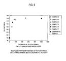
- Fig. 5 shows a relationship between the thickness of the ITO film formed on the n-type amorphous silicon layer (n-type semiconductor layer 11e) and the fill factor FF.
- Fig. 5 shows the fill factors FF of the solar cells according to Examples 2 to 7 normalized with the fill factor FF of the solar cell according to Comparative Example set to 100.
- the IHO layer was formed on the n-type amorphous silicon layer (n-type semiconductor layer 11e), and the ITO film was not formed thereon.
- the ITO film thickness ( ⁇ ) of the solar cells according to Comparative Example is therefore zero.
- the solar cells according to Examples 1 to 10 were improved in the fill factor FF and therefore improved in the output power Pmax. This is because, in each of Examples 1 to 10, the transparent conductive film was formed in the atmosphere not containing hydrogen on the n-type amorphous silicon layer (n-type semiconductor layer 11e) forming the first major surface of the photoelectric conversion body (photoelectric conversion body 11). The degradation of the surface of the n-type amorphous silicon layer (n-type semiconductor layer 11e) was prevented in each of Examples 1 to 10 in comparison with Comparative Example in which the transparent conductive film was formed on the n-type amorphous silicon layer (n-type semiconductor layer 11e) in the atmosphere containing hydrogen.
- the solar cell according to Example 2 was further improved in the fill factor FF and output power Pmax in comparison with the solar cell according to Example 1.
- the ITO film first transparent conductive film 12
- the IHO film second transparent conductive film 13
- the p-type amorphous silicon layer p-type semiconductor layer 11c
- the surface of the n-type amorphous silicon layer (n-type semiconductor layer 11e) was therefore protected by the ITO film (first transparent conductive film 12). Accordingly, the surface of the n-type amorphous silicon layer (n-type semiconductor layer 11e) was less likely to be degraded when the photoelectric conversion body (photoelectric conversion body 11) was exposed to the atmosphere containing hydrogen.
- the solar cells according to Examples 8 to 10 were further improved in the fill factor FF and output power Pmax in comparison with the solar cell according to Example 2. This is because the IHTO film containing metallic dopant had a contact resistance with the p-type amorphous silicon layer (p-type semiconductor layer 11c) lower than that of the IHO film not containing metallic dopant.
- the fill factor FF of the solar cells increased as the thickness of the ITO film (the first transparent conductive film 12 in Example 2 and the third transparent conductive film 12a in Examples 3 to 7) formed on the n-type amorphous silicon layer (n-type semiconductor layer 11e) increased from 0 to 150 ⁇ .
- the fill factor FF of the solar cells remained substantially constant when the thickness of the ITO film was 150 ⁇ or more. Accordingly, it has been found that it is preferable to form an ITO film having a thickness of 150 ⁇ or more on the n-type amorphous silicon layer (n-type semiconductor layer 11e).
- the present invention it is possible to provide a solar cell with the surface characteristics of the photoelectric conversion body prevented from being degraded and a method for manufacturing the same. Hence, the present invention is useful in the field of sunlight power generation.
Landscapes
- Photovoltaic Devices (AREA)
Abstract
Description
- The present invention relates to a solar cell including transparent conductive films formed on a photoelectric conversion body and a method for manufacturing the same.
- Solar cells are expected as a new source of energy, because solar cells are capable of directly converting light, which comes from the sun as a clean, unlimited source of energy, to electricity.
- A solar cell includes a photoelectric conversion body which has an n-type semiconductor layer and a p-type semiconductor layer and receives light to generate photogenerated carriers. The carriers are extracted from the photoelectric conversion body through electrodes formed on the n- and p-type semiconductor layers. Each electrode to be used has a layered structure of a transparent conductive film and a metallic layer in some cases. In such a case, it is desirable that the transparent conductive film have low electric resistivity.
- Herein, there is proposed a technique to form a transparent conductive film in an atmosphere containing hydrogen (see Japanese Patent Application Publication No.
Hei 2-54755 - However, if transparent conductive films are formed on the photoelectric conversion body by using the above technique, the surface characteristics of the photoelectric conversion body could be degraded. Specifically, hydrogen radicals having reducing properties could degrade the surfaces of the n- and p-type semiconductor layers when the transparent conductive films are formed.
- The present invention was made in the light of the aforementioned problem, and an object of the present invention is to provide a solar cell with the surface characteristics of the photoelectric conversion body prevented from being degraded and a method for manufacturing the same.
- The solar cell according to one characteristic of the present invention, is summarized as comprising a photoelectric conversion body configured to generate photogenerated carriers upon receiving light; a first transparent conductive film formed on a first major surface of the photoelectric conversion body; and a second transparent conductive film formed on a second major surface provided on an side opposite to the first major surface, wherein the first major surface is formed by an n-type semiconductor layer, the second major surface is formed by a p-type semiconductor layer, and a hydrogen atom content of a part of the first transparent conductive film on a side close to the n-type semiconductor layer is lower than a hydrogen atom content of the second transparent conductive film.
- In the solar cell according to a characteristic of the present invention, the hydrogen atom content of the first transparent conductive film formed on the first major surface on the n-type semiconductor layer side is lower than that of the second transparent conductive film formed on the second major surface. This can reduce the effect of hydrogen radicals on the surface of the n-type semiconductor layer forming the first major surface of the photoelectric conversion body. The degradation of the surface characteristics of the photoelectric conversion body can be therefore prevented.
- In the one characteristic of the present invention, the hydrogen atom content of a part of the first transparent conductive film on an side opposite to the n-type semiconductor layer may be higher than the hydrogen atom content of the part of the first transparent conductive film on the side close to the n-type semiconductor layer.
- In the one characteristic of the present invention, the part of the first transparent conductive film on the side close to the n-type semiconductor layer may be made of a different material from a material of the part of the first transparent conductive film on the side opposite to the n-type semiconductor layer.
- In the one characteristic of the present invention, the photoelectric conversion body is mainly made of single-crystalline silicon and each of the n-type semiconductor layer and the p-type semiconductor layer is mainly made of an amorphous silicon semiconductor.
- The method for manufacturing a solar cell according to one characteristic of the present invention, is summarized as including a photoelectric conversion body configured to generate photogenerated carriers upon receiving light, the method comprising: a step A of forming a first transparent conductive film in an atmosphere not containing hydrogen on a first major surface of the photoelectric conversion body; and a step B of forming a second transparent conductive film in an atmosphere containing hydrogen on a second major surface provided on an side opposite to the first major surface, wherein the first major surface is formed by an n-type semiconductor layer, the second major surface is formed by a p-type semiconductor layer, and in the step B, the second transparent conductive film is formed while hydrogen atoms are being supplied.
- In the one characteristic of the present invention, the step B may be performed after the step A is performed.
-
- [
Fig. 1] Fig. 1 is a plan view of asolar cell 10 according to a first embodiment of the present invention on a second major surface side. - [
Fig. 2] Fig. 2 is a cross-sectional view of thesolar cell 10 according to the first embodiment of the present invention. - [
Fig. 3] Fig. 3 is a cross-sectional view of asolar cell 10 according to a second embodiment of the present invention. [Fig. 4] Fig. 4 is a cross-sectional view of asolar cell 20 according to another embodiment. - [
Fig. 5] Fig. 5 is a view showing a relationship between thickness of an ITO film formed on an n-type amorphous silicon layer and a fill factor FF. - Next, the embodiments of the invention are described with reference to the drawings. In the following description of the drawings, identical or similar reference numerals are assigned to identical or similar components. However, the drawings are schematic, thus it should be noted that the dimensions are not shown to scale. Accordingly, specific dimensions should be recognized in consideration of the following description. Also, there are inevitably included some portions of the drawings between which a dimensional relationship and/or a scale are inconsistent.
- The schematic structure of a
solar cell 10 according to a first embodiment of the present invention is described below with reference toFigs. 1 and 2. Fig. 1 is a plan view of thesolar cell 10 on a second major surface S2 side.Fig. 2 is an A-A cross-sectional view ofFig. 1 . - As shown in
Figs. 1 and 2 , thesolar cell 10 includes asolar cell substrate 1, fine-line electrodes 2, and connecting electrodes 3. - As shown in
Fig. 2 , thesolar cell substrate 1 includes aphotoelectric conversion body 11, a first transparentconductive film 12, and a second transparentconductive film 13. Thephotoelectric conversion body 11 is configured to generate photogenerated carriers upon receiving light. Thesolar cell substrate 1 includes a first major surface S1 (the lower surface inFig. 2 ) and a second major surface S2 (the upper surface inFig. 2 ) provided on the opposite side to the first major surface S1. The structure of thesolar cell substrate 1 is described later. - The fine-
line electrodes 2 are collecting electrodes configured to collect photogenerated carriers from thephotoelectric conversion body 11. The fine-line electrodes 2 are formed on the second major surface S2 of thesolar cell substrate 1 along a first direction substantially parallel to a side of thesolar cell substrate 1 as shown inFig. 1 . Some of the plurality of fine-line electrodes 2 are arranged substantially at regular intervals in a second direction substantially orthogonal to the first direction. The other fine-line electrodes 2 (not shown) are formed on the first major surface S1 of thesolar cell substrate 1 in a similar manner to those on the second major surface S2 of thesolar cell substrate 1. The fine-line electrodes 2 formed on the second major surface S2 of thesolar cell substrate 1 collect carriers from thephotoelectric conversion body 11 through the second transparentconductive film 13 later described. The fine-line electrodes 2 formed on the first major surface S1 of thesolar cell substrate 1 collect carriers from thephotoelectric conversion body 11 through the first transparentconductive film 12 later described. - The fine-
line electrodes 2 can be formed, for example, by printing resin-type conductive paste which includes a resin material as a binder and conductive particles such as silver particles as a filler or sintered-type conductive paste containing silver powder, glass frit, organic vehicle, organic solvent, and the like (so-called ceramic paste) by using a printing process. Each fine-line electrode 2 may be formed as a metallic film by deposition. The number and size of the fine-line electrodes 2 can be set to proper values in consideration of the size of thephotoelectric conversion body 11 and the like. - The connecting electrodes 3 are electrodes connected to wiring materials (not shown) electrically connecting a plurality of the
solar cells 10 in series or in parallel. The connecting electrodes 3 are formed on the second major surface S2 of thesolar cell substrate 1 along the second direction as shown inFig. 1 . Accordingly, some of the connecting electrodes 3 intersect the plurality of fine-line electrodes 2 and are electrically connected to the plurality of fine-line electrodes 2. The other connecting electrodes 3 (not shown) are formed on the first major surface S1 of thesolar cell substrate 1 in a similar manner to the first major surface S2 of thesolar cell substrate 1. The connecting electrodes 3 can be formed by printing or deposition in a similar way to the fine-line electrodes 2. The number and size of the connecting electrodes 3 can be set to proper values in consideration of the size of thephotoelectric conversion body 11 and the like. - Next, a description is given of an example of the structure of the
solar cell substrate 1 according to the first embodiment of the present invention with reference toFig. 2 . - The
solar cell substrate 1 includes thephotoelectric conversion body 11 and the first and second transparentconductive films Fig. 2 . - The
photoelectric conversion body 11 includes the first major surface S1 (the lower surface inFig. 2 ) and the second major surface S2 (the upper surface inFig. 2 ) provided on the opposite side to the first major surface S1. Thephotoelectric conversion body 11 receives light through the first or second major surface S1 or S2 of thephotoelectric conversion body 11 to generate photogenerated carriers. Each of the photogenerated carriers refers to a pair of a hole and an electron generated upon thephotoelectric conversion body 11 absorbing solar light. - The
photoelectric conversion body 11 includes an n-type substrate 11a, an i-type semiconductor layer 11b, a p-type semiconductor layer 11c, an i-type semiconductor layer 11d, and an n-type semiconductor layer 11e as shown inFig. 2 . - The n-
type substrate 11a is a main body of thephotoelectric conversion body 11. For the n-type substrate 11a, an n-type single-crystalline silicon substrate can be used, for example. - The p-
type semiconductor layer 11e is formed on the second major surface S2 side of the n-type substrate 11a with the i-type semiconductor layer 11b interposed therebetween. On the other hand, the n-type semiconductor layer 11e is formed on the first major surface S1 side of the n-type substrate 11a with the i-type semiconductor layer 11d interposed therebetween. In other words, the second major surface S2 of thephotoelectric conversion body 11 is formed by the p-type semiconductor layer 11c, and the first major surface S1 of thephotoelectric conversion body 11 is formed by the n-type semiconductor layer 11e. - For the i-
type semiconductor layer 11b, p-type semiconductor layer 11c, i-type semiconductor layer 11d, and n-type semiconductor layer 11e, for example, an i-type amorphous semiconductor layer, a p-type amorphous semiconductor layer, an i-type amorphous semiconductor layer, and a n-type amorphous semiconductor layer can be used, respectively. In such a case, it is preferable that the i-type semiconductor layers 11b and 11d constituted by i-type amorphous semiconductor layers have such thicknesses that the i-type semiconductor layers 11b and 11d substantially do not contribute to power generation. For example, the thicknesses of the i-type semiconductor layers 11b and 11d are preferably in a range from several Å to 250 Å. The amorphous semiconductors can be silicon-based semiconductors such as amorphous silicon, amorphous silicon carbide, amorphous silicon germanium, and microcrystalline silicon. - The structure of the
photoelectric conversion body 11 is not limited to the aforementioned structure. For example, thephotoelectric conversion body 11 does not need to include the i-type semiconductor layers 11b and 11d and may have another structure. - As shown in
Fig. 2 , the first transparentconductive film 12 is formed on the n-type semiconductor layer 11e forming the first major surface S1 of thephotoelectric conversion body 11. The first transparentconductive film 12 has translucency and conductivity. For the first transparentconductive layer 12, a metal oxide such as indium oxide (In2O3), zinc oxide (ZnO), tin oxide (SnO2), or titanium oxide (TiO2) can be used. These metal oxides may be doped with a dopant such as tin (Sn), zinc (Zn), tungsten (W), antimony (Sb), titanium (Ti), cerium (Ce), zirconium (Zr), molybdenum (Mo), aluminum (Al), or gallium (Ga). The concentration of the dopant can be 0 to 20 wt%. - As shown in
Fig. 2 , the second transparentconductive film 13 is formed on the p-type semiconductor layer 11c forming the second major surface S2 of thephotoelectric conversion body 11. The second transparentconductive film 13 has translucency and conductivity. Similarly to the first transparentconductive film 12, for the second transparentconductive film 13, a metal oxide such as indium oxide (In2O3), zinc oxide (ZnO), tin oxide (SnO2), or titanium oxide (TiO2) can be used. These metal oxides may be doped with a dopant such as tin (Sn), zinc (Zn), tungsten (W), antimony (Sb), titanium (Ti), cerium (Ce), zirconium (Zr), molybdenum (Mo), aluminum (Al), or gallium (Ga). The concentration of the dopant can be 0 to 20 wt%. The materials constituting the second transparentconductive film 13 may be either the same as or different from materials constituting the first transparentconductive film 12. - In this embodiment, the hydrogen atom content of the first transparent
conductive film 12 is lower than that of the second transparentconductive film 13. Accordingly, a metal oxide formed in an atmosphere not containing hydrogen can be used for the first transparentconductive film 12 while a metal oxide formed in an atmosphere supplying hydrogen atoms (an atmosphere containing hydrogen) can be used for the second transparentconductive film 13. - Next, a method for manufacturing the
solar cell 10 according to the first embodiment of the present invention is described. First, the n-type substrate 11a is etched to form fine roughness on the first and second major surfaces S1 and S2 sides. - Next, the i-type and p-type semiconductor layers 11b and 11c are sequentially stacked on the second major surface S2 side of the n-
type substrate 11a using CVD or the like. The i-type and n-type semiconductor layers type substrate 11a in a similar manner. Thephotoelectric conversion body 11 is thus formed. - Next, the first transparent
conductive film 12 is formed on the n-type semiconductor layer 11e by using a sputtering method or the like in an atmosphere not containing hydrogen such as an Ar and O2 atmosphere. The atmosphere not containing hydrogen refers to an atmosphere not actively supplying hydrogen atoms. The hydrogen atom contents of the transparent conductive films formed in the atmosphere not containing hydrogen are about 1.0×10²⁰ to 5.2×10²⁰ (atoms/cc). - Next, by using a sputtering method or the like, the second transparent
conductive film 13 is formed on the p-type semiconductor layer 11c in an atmosphere containing hydrogen. Specifically, the second transparentconductive film 13 is formed in an Ar, O2, and H2O atmosphere, an Ar, O2, and H2 atmosphere, or the like where hydrogen atoms are being supplied thereto. The hydrogen atom content of the second transparentconductive film 13 is therefore higher than that of the first transparentconductive film 12. Thesolar cell substrate 1 is thus formed. Preferably, the process to form the second transparentconductive film 13 is performed after the process to form the first transparentconductive film 12 is performed. - Next, epoxy-based thermosetting-type silver paste is placed on the second major surface S2 of the
solar cell substrate 1 in a predetermined pattern by using a printing process such as screen printing or off-set printing. In a similar manner, epoxy-based thermosetting-type silver paste is placed on the first major surface S1 of thesolar cell 1 in a predetermined pattern. The silver paste is heated under predetermined conditions for volatilization of the solvent and is then further heated for final drying. Herein, the predetermined patterns have the shapes corresponding to the fine-line electrodes 2 extending along the first direction and the connecting electrodes 3 extending along the second direction as shown inFig. 1 . Thesolar cell 10 is thus manufactured. - In the
solar cell 10 according to the first embodiment of the present invention, the first transparentconductive film 12 is formed on the n-type semiconductor layer 11e, which forms the first major surface S1 of thephotoelectric conversion body 11, in the atmosphere not containing hydrogen. Moreover, the second transparentconductive film 13 is formed on the p-type semiconductor layer 11c, which forms the second major surface S2 of thephotoelectric conversion body 11, in the atmosphere containing hydrogen. The hydrogen atom content of the first transparentconductive film 12 formed on the first major surface S1 of thephotoelectric conversion body 11 is therefore lower than that of the second transparentconductive film 13 formed on the second major surface S2 of thephotoelectric conversion body 11. - The applicant examined the influence of hydrogen radicals on the surfaces of the p-type and n-
type semiconductor layer type semiconductor layer 11c forming the second major surface S2 of thephotoelectric conversion body 11 and on the n-type semiconductor layer 11e forming the first major surface S1 of thephotoelectric conversion body 11. As a result, the applicant found that the surface of the n-type semiconductor layer 11e was more likely to be degraded by hydrogen radicals. - Accordingly, the first transparent
conductive film 12 is formed in the atmosphere not containing hydrogen on the n-type semiconductor layer 11e, the surface of which is more likely to be degraded in the atmosphere containing hydrogen, so that the surface of the n-type semiconductor layer 11e can be prevented from being degraded by hydrogen radicals. On the other hand, the second transparentconductive film 13 is formed on the p-type semiconductor layer 11c, which is less affected by hydrogen radicals in the atmosphere containing hydrogen than the n-type semiconductor layer 11e, with hydrogen atoms being actively introduced thereto. This can provide increased translucency and reduced electric resistivity to the second transparentconductive film 13. As described above, in thesolar cell 10 according to the first embodiment of the present invention, it is possible to prevent the degradation of the surface characteristics of thephotoelectric conversion body 11. - Moreover, since the second transparent
conductive film 13 is formed on the p-type semiconductor layer 11c after the first transparentconductive film 12 is formed on the n-type semiconductor layer 11e, the surface of the n-type semiconductor layer 11e is protected by the first transparentconductive film 12. This can further reduce the influence of hydrogen radicals on the surface of the n-type semiconductor layer 11e when the second transparentconductive film 13 is formed in the atmosphere containing hydrogen. - Hereinbelow, a second embodiment of the present invention is described. The following description is mainly about the difference between the aforementioned first embodiment and the second embodiment. Specifically, in the aforementioned first embodiment, the hydrogen atom content of the first transparent
conductive film 12 on the n-type semiconductor layer 11e side is substantially the same as that of the first transparentconductive film 12 on the opposite side to the n-type semiconductor layer 11e. In contrast, in the second embodiment, the hydrogen atom content of the first transparentconductive film 12 on the n-type semiconductor layer 11e side is different from that of the first transparentconductive film 12 on the opposite side to the n-type semiconductor layer 11e. The schematic structure of thesolar cell 10 according to the second embodiment of the present invention is substantially the same as that of thesolar cell 10 according to the first embodiment, and the description thereof is omitted herein. - An example of the structure of the
solar cell substrate 1 according to the second embodiment of the present invention is described with reference toFig. 3 . - The
solar cell substrate 1 includes thephotoelectric conversion body 11, the first transparentconductive film 12, and the second transparentconductive film 13 as shown inFig. 3 . The structures of thephotoelectric conversion body 11 and second transparentconductive film 13 are substantially the same as those of the aforementioned first embodiment, and the description thereof is omitted. - The first transparent
conductive film 12 includes a third transparentconductive film 12a and a fourth transparentconductive film 12b as shown inFig. 3 . The third transparentconductive film 12a is formed on the n-type semiconductor layer 11e forming the first major surface S1 of thephotoelectric conversion body 11. The fourth transparentconductive film 12b is formed on the third transparentconductive film 12a. The third and fourth transparentconductive films conductive films - In this embodiment, the hydrogen atom content of the fourth transparent
conductive film 12b is higher than that of the third transparentconductive film 12a. In other words, the hydrogen atom content of a half of the first transparentconductive film 12 on the opposite side to the n-type semiconductor layer 11e is higher than that of the other half on the n-type semiconductor layer 11e side. Moreover, the hydrogen atom content of the third transparentconductive film 12a is lower than that of the second transparentconductive film 13. In other words, the hydrogen atom content of the half of the first transparentconductive film 12 on the n-type semiconductor layer 11e side is lower than that of the second transparentconductive film 13. - Accordingly, for example, for the third transparent
conductive film 12a, a metallic oxide formed in the atmosphere not containing hydrogen can be used while a metallic oxide formed in the atmosphere supplying hydrogen atoms (the atmosphere containing hydrogen) in a similar manner to the second transparentconductive film 13 can be used for the fourth transparentconductive film 12b. The materials constituting the second, third, and fourth transparentconductive films - Next, a method for manufacturing the
solar cell 10 according to the second embodiment of the present invention is described. - First, the
photoelectric conversion body 11 is formed in the same way as the aforementioned first embodiment. Next, the third transparentconductive film 12a is formed on the n-type semiconductor layer 11e, which forms the first major surface S1 of thephotoelectric conversion body 11, by using a sputtering method or the like in the atmosphere not containing hydrogen such as an Ar and O2 atmosphere. - Next, the second transparent
conductive film 13 is formed on the p-type semiconductor layer 11c by using a sputtering method or the like in the atmosphere containing hydrogen. Specifically, the second transparentconductive film 13 is formed in an Ar, O2, and water vapor atmosphere, an Ar, O2, and hydrogen atmosphere, or the like where hydrogen atoms are being supplied. The hydrogen atom content of the second transparentconductive film 13 is therefore made higher than that of the third transparentconductive film 12a. - Next, the fourth transparent
conductive film 12b is formed on the third transparentconductive film 12a by using a sputtering method or the like in the atmosphere containing hydrogen. Specifically, the fourth transparentconductive film 12b is formed in an Ar, O2, and water vapor atmosphere, an Ar, O2, and hydrogen atmosphere, or the like where hydrogen atoms are being supplied. The hydrogen atom content of the fourth transparentconductive film 12b is therefore made higher than that of the third transparentconductive film 12a. The first transparentconductive film 12 is thus formed. Thesolar cell substrate 1 is formed in such a manner. - Next, the fine-
line electrodes 2 and connecting electrodes 3 are formed in the same way as the aforementioned first embodiment. Thesolar cell 10 is thus formed. - In the
solar cell 10 according to the second embodiment of the present invention, the first transparentconductive film 12 formed on the n-type semiconductor layer 11e includes the third and fourth transparentconductive films conductive film 12a is formed on the n-type semiconductor layer 11e in the atmosphere not containing hydrogen, and the fourth transparentconductive film 12b is formed on the third transparentconductive film 12a in the atmosphere containing hydrogen. - Accordingly, it is possible to increase the translucency of the overall first transparent
conductive film 12 and reduce the electrical resistivity thereof without degrading the surface of the n-type semiconductor layer 11e in comparison with the case where the hydrogen atom content of the first transparentconductive film 12 on the n-type semiconductor layer 11e side is substantially equal to that of the first transparentconductive film 12 on the opposite side to the n-type semiconductor layer 11e. - The present invention has been described by using the embodiments of the present invention. However, it should not be understood that the description and drawings which constitute part of this disclosure limit the present invention. From this disclosure, various alternative embodiments, examples, and operation techniques will be easily found by those skilled in the art.
- For example, in the aforementioned first and second embodiments, the description is given of the case where the present invention is applied to the crystal-type solar cell; however, the present invention may be applied to thin film-type solar cells.
Fig. 4 is a cross-sectional view of a thin film-typesolar cell 20. As shown inFig. 4 , the thin film-typesolar cell 20 includes asubstrate 21 having translucency, a fifth transparentconductive film 22, a photoelectric conversion body 23 configured to receive light and generate photogenerated carriers, a sixth transparentconductive film 24, and a rear electrode layer 25. The photoelectric conversion body 23 has a structure in which a p-type semiconductor layer 23a, an i-type semiconductor layer 23b, and an n-type semiconductor layer 23c are sequentially stacked from thesubstrate 21 side. In thesolar cell 20 having such a structure, similarly to the aforementioned first and second embodiments, the fifth transparentconductive film 22 is formed on the )substrate 21 in the atmosphere containing hydrogen, and the sixth transparentconductive film 24 is formed on the n-type semiconductor layer 23c in the atmosphere not containing hydrogen. This can prevent degradation of the surface of the n-type semiconductor layer 23c (corresponding to "the second surface S2" of the aforementioned embodiments). Moreover, the translucency of the fifth transparentconductive film 22 can be increased, and the electrical resistivity thereof can be reduced. Furthermore, since the p-type semiconductor layer 23a is formed after the fifth transparent conductive film 22 ) is formed, it is possible to prevent degradation of the surface of the p-type semiconductor layer 23a on the fifth transparentconductive film 22 side (corresponding to "the first surface S1" of the aforementioned embodiment). The structure of thesolar cell 20 is not limited to the structure shown inFig. 4 and may be a structure in which the fifth transparentconductive film 22, photoelectric conversion body 23, sixth transparentconductive film 24, rear electrode layer 25, andsubstrate 21 are stacked in this order. Moreover, the structure of the photoelectric conversion body 23 is not limited to the structure shown inFig. 4 and may be a structure in which the n-type, i-type, and p-type semiconductor layers substrate 21 side or a structure in which the p-type and n-type semiconductor layers substrate 21 side. For the p-type, i-type, and n-type semiconductor layers - The aforementioned first and second embodiments describe about the case where the fine-
line electrodes 2 and connecting electrodes 3 having the same shapes as those formed on the second major surface S2 of thesolar cell substrate 1 are formed on the first major surface S1 of thesolar cell substrate 1, but the present invention is not limited to such a case. For example, the fine-line electrodes 2 may be formed so as to cover substantially all over any one of the first and second major surfaces S1 and S2 of thesolar cell substrate 1. - The aforementioned first and second embodiments describe the case where the
photoelectric conversion body 11 includes the n-type substrate 11a, i-type semiconductor layer 11b, p-type semiconductor layer 11c, i-type semiconductor layer 11d, and n-type semiconductor layer 11e, but the present invention is not limited to such a case. For example, thephotoelectric conversion body 11 may include only the p-type and n-type semiconductor layers 11c and 11e. - In the aforementioned second embodiment, the third and fourth transparent
conductive films conductive film 12 so that the hydrogen atom content of the part of the first transparentconductive film 12 on the opposite side to the n-type semiconductor layer 11e is higher than that of the part of the first transparentconductive film 12 on the n-type semiconductor layer 11e side. However, the present invention is not limited to this. Specifically, the first transparentconductive film 12 composed of a single film may be formed so that the hydrogen atom content thereof increases from the n-type semiconductor layer 11e side toward the opposite side to the n-type semiconductor layer 11e. The first transparentconductive film 12 having such a structure can be formed, for example, by employing the atmosphere not containing hydrogen as the condition for forming the first transparentconductive film 12 in a first part of the forming process and then increasing the supply amount of hydrogen atoms stepwisely so that the condition for forming the first transparentconductive film 12 can be the atmosphere containing hydrogen in a last part of the forming process. - As described above, the present invention naturally includes various embodiments which are not described herein. Accordingly, the technical scope of the present invention should be determined only by the matters to define the invention in the scope of claims regarded as appropriate based on the description.
- Hereinbelow, the solar cell according to the present invention is specifically described with examples. However, the present invention is not limited to the following examples and can be implemented with appropriate modification without changing the scope of the present invention.
- First, a comparison was made between hydrogen atom contents of transparent conductive films formed in the atmosphere not containing hydrogen and hydrogen atom contents of transparent conductive films formed in the atmosphere containing hydrogen. Specifically, hydrogen atom contents of test films A and B were measured by SIMS. Herein, the test films A were In2O3 films formed in the atmosphere not containing hydrogen by using a sputtering method, and the test films B were In2O3 formed in the atmosphere containing hydrogen by using a sputtering method. The measurement results of the hydrogen atom contents of the test films are shown in Table 1.
[Table 1] Test film Hydrogen atom content (atoms/cc) A(In2O3 films formed in atmosphere not containing hydrogen) 1.0×10²⁰ - 5.2×10²⁰ B(In2O3 formed in atmosphere containing hydrogen) 1.6×10²¹ - 2.1×10²¹ - As shown in Table 1, it was found that the hydrogen atom contents of the test films A, which were In2O3 films formed in the atmosphere not containing hydrogen, were about 1.0×10²⁰ to 5.2×10²⁰ (atoms/cc) while the hydrogen atom contents of the test films B, which were In2O3 films formed in the atmosphere containing hydrogen to actively incorporate hydrogen atoms, were 1.6×10²¹ to 2.1×10²¹ (atoms/cc).
- Next, solar cells according to Examples 1 to 7 and Comparative Example were manufactured in the following manner, and comparisons were made in terms of characteristic values including open-circuit voltage Voc, short-circuit current Isc, fill factor FF, and output power Pmax.
- The solar cell according to Example 1 was manufactured as follows. First, an n-type single-crystalline silicon substrate (n-
type substrate 11a) with a thickness of 200 µm was anisotropically etched with an alkaline aqueous solution to form fine roughness on the first and second major surfaces. The first and second major surfaces of the n-type substrate 11a were cleaned to remove impurities. - Next, on the second major surface side of the n-type single-crystalline silicon substrate (n-
type substrate 11a), an i-type amorphous silicon layer (i-type semiconductor layer 11b) and a p-type amorphous silicon layer (p-type semiconductor layer 11c) were sequentially stacked by using a plasma CVD method or the like. Next, on the first major surface side of the n-type single-crystalline silicon substrate (n-type substrate 11a), an i-type amorphous silicon layer (i-type semiconductor layer 11d) and an n-type amorphous silicon layer (n-type semiconductor layer 11c) were sequentially stacked. The i-type amorphous silicon layer (i-type semiconductor layer 11b), p-type amorphous silicon layer (p-type semiconductor layer 11c), i-type amorphous silicon layer (i-type semiconductor layer 11d), and n-type amorphous silicon layer (n-type semiconductor layer 11c) each have a thickness of 5 mm. The photoelectric conversion body (photoelectric conversion body 11) was thus formed. - Next, on the p-type amorphous silicon layer (p-
type semiconductor layer 11c), an IHO film (second transparent film 13) was formed by using a sputtering method in an Ar, O2, and water vapor atmosphere (the atmosphere containing hydrogen). The IHO film (second transparent conductive film 13) was an In2O3 film formed in the atmosphere containing hydrogen to have a hydrogen atom content higher than that of an ITO film (first transparent conductive film 12) later described. The IHO film (second transparent conductive film 13) had a thickness of 1000 Å and was formed at room temperature. - Next, on the n-type amorphous silicon layer (n-
type semiconductor layer 11e), the ITO film (first transparent conductive film 12) was formed by using a sputtering method in an Ar and O2 atmosphere (atmosphere not containing hydrogen). The ITO film (first transparent conductive film 12) had a thickness of 1000 Å and was formed at room temperature. In short, in Example 1, the ITO film (first transparent conductive film 12) was formed on the n-type amorphous silicon layer (n-type semiconductor layer 11e) after the IHO film (second transparent conductive film 13) was formed on the p-type amorphous silicon layer (p-type semiconductor layer 11c). The solar cell substrate (solar cell substrate 1) was thus formed. - Next, paste including a conductive filler mainly containing Ag and thermosetting resin was placed in predetermined patterns on the second and first major surfaces of the solar cell substrate (solar cell substrate 1) by using a screen printing method and was then annealed at 200°C. Fine-line electrodes (fine-line electrodes 2) and connecting electrodes (connecting electrodes 3) were thus formed. The solar cell according to Example 1 was formed in such a manner.
- The solar cell according to Example 2 was manufactured in the following manner. First the photoelectric conversion body (photoelectric conversion body 11) was formed in the same way as Example 1 described above.
- Next, on the n-type amorphous silicon layer (n-
type semiconductor layer 11e), the ITO film (first transparent conductive film 12) was formed by using a sputtering method in an Ar and O2 atmosphere (atmosphere not containing hydrogen). The ITO film (first transparent conductive film 12) had a thickness of 1000 Å and was formed at room temperature. - Next, on the p-type amorphous silicon layer (p-
type semiconductor layer 11c), an IHO film (second transparent film 13) was formed by using a sputtering method in an Ar, O2, and water vapor atmosphere (the atmosphere containing hydrogen). The IHO film (second transparent conductive film 13) had a thickness of 1000 Å and was formed at room temperature. In short, in Example 2, the IHO film (second transparent conductive film 13) was formed on the p-type amorphous silicon layer (p-type semiconductor layer 11c) after the ITO film (first transparent conductive film 12) was formed on the n-type amorphous silicon layer (n-type semiconductor layer 11e) in a reverse order to that in Example 1. The solar cell substrate (solar cell substrate 1) was thus formed. - Next, fine-line electrodes (fine-line electrodes 2) and connecting electrodes (connecting electrodes 3) were formed in the same way as Example 1 described above. The solar cell according to Example 2 was formed in such a manner.
- The solar cell according to Example 3 was manufactured in the following manner. First the photoelectric conversion body (photoelectric conversion body 11) was formed in the same way as Example 1 described above.
- Next, on the n-type amorphous silicon layer (n-
type semiconductor layer 11e), the ITO film (third transparentconductive film 12a) was formed by using a sputtering method in an Ar and O2 atmosphere (atmosphere not containing hydrogen). The ITO film (third transparentconductive film 12a) had a thickness of 500 Å and was formed at room temperature. - Next, on the p-type amorphous silicon layer (p-
type semiconductor layer 11c), an IHO film (second transparent film 13) was formed by using a sputtering method in an Ar, O2, and water vapor atmosphere (the atmosphere containing hydrogen). The IHO film (second transparent conductive film 13) had a thickness of 1000 Å and was formed at room temperature. - Next, on the ITO film (third transparent
conductive film 12a), an IHO film (fourthtransparent film 12b) was formed by using a sputtering method in an Ar, O2, and water vapor atmosphere (the atmosphere containing hydrogen). The IHO film (fourthtransparent film 12b) was an In2O3 film formed in the atmosphere containing hydrogen to have a hydrogen atom content higher than that of the ITO film (third transparentconductive film 12a). The IHO film (fourthtransparent film 12b) had a thickness of 500 Å and was formed at room temperature. - Next, fine-line electrodes (fine-line electrodes 2) and connecting electrodes (connecting electrodes 3) were formed in the same way as Example 2 described above. The solar cell according to Example 3 was formed in such a manner.
- In Example 4, the thickness of the ITO film (third transparent
conductive film 12a) in Example 3 described above was changed to 200 Å, and the thickness of the IHO film (fourth transparentconductive film 12b) was changed to 800 Å. The structures of the solar cells according to Example 4 and Example 3 described above were the same except that the thicknesses of the ITO film (third transparentconductive film 12a) and the IHO film (fourth transparentconductive film 12b) were changed. - In Example 5, the thickness of the ITO film (third transparent
conductive film 12a) in Example 3 described above was changed to 150 Å, and the thickness of the IHO film (fourth transparentconductive film 12b) was changed to 850 Å. The structures of the solar cells according to Example 5 and Example 3 described above were the same except that the thicknesses of the ITO film (third transparentconductive film 12a) and the IHO film (fourth transparentconductive film 12b) were changed. - In Example 6, the thickness of the ITO film (third transparent
conductive film 12a) in Example 3 described above was changed to 100 Å, and the thickness of the IHO film (fourth transparentconductive film 12b) was changed to 900 Å. The structures of the solar cells according to Example 6 and Example 3 described above were the same except that the thicknesses of the ITO film (third transparentconductive film 12a) and the IHO film (fourth transparentconductive film 12b) were changed. - In Example 7, the thickness of the ITO film (third transparent
conductive film 12a) in Example 3 described above was changed to 75 Å, and the thickness of the IHO film (fourth transparentconductive film 12b) was changed to 925 Å. The structures of the solar cells according to Example 7 and Example 3 described above were the same except that the thicknesses of the ITO film (third transparentconductive film 12a) and the IHO film (fourth transparentconductive film 12b) were changed. - In Example 8, an ITO film (first transparent conductive film 12) was formed on an n-type amorphous silicon layer (n-
type semiconductor layer 11e) of the photoelectric conversion body (photoelectric conversion body 11) in the same way as Example 2 described above. The ITO film (first transparent conductive film 12) had a thickness of 1000 Å and was formed at room temperature. - Next, on the p-type amorphous silicon layer (p-
type semiconductor layer 11c), an IHTO film (second transparent film 13) was formed by using a sputtering method in an Ar, O2, and water vapor atmosphere (the atmosphere containing hydrogen). The IHTO film (second transparent conductive film 13) was an ITO film formed in the atmosphere containing hydrogen to have a high hydrogen atom content. The IHTO film had a thickness of 1000 Å and was formed at room temperature. The solar cell substrate (solar cell substrate 1) was thus formed. - Next, fine-line electrodes (fine-line electrodes 2) and connecting electrodes (connecting electrodes 3) were formed in the same way as Example 2 described above. The solar cell according to Example 8 was thus formed.
- In Example 9, the photoelectric conversion body (photoelectric conversion body 11) was formed in the same way as Example 2 described above.
- Next, an IWO film (first transparent conductive film 12) was formed on the n-type amorphous silicon layer (n-
type semiconductor layer 11e) by using a sputtering method in the Ar and O2 atmosphere (atmosphere not containing hydrogen). The IWO film (first transparent conductive film 12) was an In2O3 film doped with tungsten (W). The IWO film (first transparent conductive film 12) had a thickness of 1000 Å and was formed at room temperature. - Next, on the p-type amorphous silicon layer (p-
type semiconductor layer 11c), an IHWO film (second transparent film 13) was formed by using a sputtering method in an Ar, O2, and water vapor atmosphere (the atmosphere containing hydrogen). The IHWO film (second transparent conductive film 13) was an IWO film formed in the atmosphere containing hydrogen to have a high hydrogen atom content. The IHWO film (second transparent conductive film 13) had a thickness of 1000 Å and was formed at room temperature. The solar cell substrate (solar cell substrate 1) was thus formed. - Next, fine-line electrodes (fine-line electrodes 2) and connecting electrodes (connecting electrodes 3) were formed in the same way as Example 2 described above. The solar cell according to Example 9 was thus formed.
- In Example 10, the photoelectric conversion body (photoelectric conversion body 11) was formed in the same way as Example 2 described above.
- Next, an ICO film (first transparent conductive film 12) was formed on the n-type amorphous silicon layer (n-
type semiconductor layer 11e) by using a sputtering method in the Ar and O2 atmosphere (atmosphere not containing hydrogen). The ICO film (first transparent conductive film 12) was an In2O3 film doped with cerium (Ce). The ICO film (first transparent conductive film 12) had a thickness of 1000 Å and was formed at room temperature. - Next, on the p-type amorphous silicon layer (p-
type semiconductor layer 11c), an IHCO film (second transparent film 13) was formed by using a sputtering method in an Ar, O2, and water vapor atmosphere (the atmosphere containing hydrogen). The IHCO film (second transparent conductive film 13) was an ICO film formed in the atmosphere containing hydrogen to have a high hydrogen atom content. The IHCO film (second transparent conductive film 13) had a thickness of 1000 Å and was formed at room temperature. The solar cell substrate (solar cell substrate 1) was thus formed. - Next, fine-line electrodes (fine-line electrodes 2) and connecting electrodes (connecting electrodes 3) were formed in the same way as Example 2 described above. The solar cell according to Example 10 was thus formed.
- The solar cell according to Comparative Example was manufactured in the following manner. First the photoelectric conversion body (photoelectric conversion body 11) was formed in the same way as Example 1 described above.
- Next, on the n-type amorphous silicon layer (n-
type semiconductor layer 11e), a first IHO film was formed by using a sputtering method in an Ar, O2, and water vapor atmosphere (the atmosphere containing hydrogen). The first IHO film had a thickness of 1000 Å and was formed at room temperature. - Next, on the p-type amorphous silicon layer (p-
type semiconductor layer 11c), a second IHO film (second transparent film 13) was formed by using a sputtering method in an Ar, O2, and water vapor atmosphere (the atmosphere containing hydrogen). The second IHO film had a thickness of 1000 Å and was formed at room temperature. The solar cell substrate (solar cell substrate 1) was thus formed. - Next, fine-line electrodes (fine-line electrodes 2) and connecting electrodes (connecting electrodes 3) were formed in the same way as Example 1 described above. The solar cell according to Comparative Example was formed in such a manner.
- The characteristic values including the open-circuit voltage Voc, short-circuit current Isc, fill factor FF, and output power Pmax were measured for the solar cells according to Examples 1 to 10 and Comparative Example described above. The results of the measurement are shown in Table 2. Table 2 shows the characteristic values of the solar cells according to Examples 1 to 10 normalized with the characteristic values of the solar cell according to Comparative Example set to 100.
Fig. 5 shows a relationship between the thickness of the ITO film formed on the n-type amorphous silicon layer (n-type semiconductor layer 11e) and the fill factor FF.Fig. 5 shows the fill factors FF of the solar cells according to Examples 2 to 7 normalized with the fill factor FF of the solar cell according to Comparative Example set to 100. Moreover, in the solar cell according to Comparative Example, the IHO layer was formed on the n-type amorphous silicon layer (n-type semiconductor layer 11e), and the ITO film was not formed thereon. InFig. 5 , the ITO film thickness (Å) of the solar cells according to Comparative Example is therefore zero.[Table 2] Open-circuit voltage (Voc) Short-circuit current (Isc) Fill factor (FF) Output power (Pmax) Example 1 100.7 99.8 111.0 111.5 Example 2 100.9 99.6 113.8 114.4 Example 3 100.7 99.7 114.1 114.5 Example 4 100.5 99.5 113.0 113.1 Example 5 100.6 99.9 113.4 114.0 Example 6 100.5 100.2 111.2 112.0 Example 7 100.4 99.4 107.9 107.8 Example 8 100.7 99.5 117.5 117.7 Example 9 100.6 99.9 117.0 117.6 Example 10 100.2 100.3 116.5 117.1 Comparative Example 100.0 100.0 100.0 100.0 - As shown in Table 2, it was found that, in comparison with the solar cell according to Comparative Example, the solar cells according to Examples 1 to 10 were improved in the fill factor FF and therefore improved in the output power Pmax. This is because, in each of Examples 1 to 10, the transparent conductive film was formed in the atmosphere not containing hydrogen on the n-type amorphous silicon layer (n-
type semiconductor layer 11e) forming the first major surface of the photoelectric conversion body (photoelectric conversion body 11). The degradation of the surface of the n-type amorphous silicon layer (n-type semiconductor layer 11e) was prevented in each of Examples 1 to 10 in comparison with Comparative Example in which the transparent conductive film was formed on the n-type amorphous silicon layer (n-type semiconductor layer 11e) in the atmosphere containing hydrogen. - As shown in Table 2, it was found that the solar cell according to Example 2 was further improved in the fill factor FF and output power Pmax in comparison with the solar cell according to Example 1. This is because the ITO film (first transparent conductive film 12) was formed on the n-type amorphous silicon layer (n-
type semiconductor layer 11e) in the atmosphere not containing hydrogen before the IHO film (second transparent conductive film 13) was formed on the p-type amorphous silicon layer (p-type semiconductor layer 11c) in the atmosphere containing hydrogen. The surface of the n-type amorphous silicon layer (n-type semiconductor layer 11e) was therefore protected by the ITO film (first transparent conductive film 12). Accordingly, the surface of the n-type amorphous silicon layer (n-type semiconductor layer 11e) was less likely to be degraded when the photoelectric conversion body (photoelectric conversion body 11) was exposed to the atmosphere containing hydrogen. - As shown in Table 2, it was found that the solar cells according to Examples 8 to 10 were further improved in the fill factor FF and output power Pmax in comparison with the solar cell according to Example 2. This is because the IHTO film containing metallic dopant had a contact resistance with the p-type amorphous silicon layer (p-
type semiconductor layer 11c) lower than that of the IHO film not containing metallic dopant. - Moreover, as shown in
Fig. 5 , the fill factor FF of the solar cells increased as the thickness of the ITO film (the first transparentconductive film 12 in Example 2 and the third transparentconductive film 12a in Examples 3 to 7) formed on the n-type amorphous silicon layer (n-type semiconductor layer 11e) increased from 0 to 150 Å. The fill factor FF of the solar cells remained substantially constant when the thickness of the ITO film was 150 Å or more. Accordingly, it has been found that it is preferable to form an ITO film having a thickness of 150 Å or more on the n-type amorphous silicon layer (n-type semiconductor layer 11e). - According to the present invention, it is possible to provide a solar cell with the surface characteristics of the photoelectric conversion body prevented from being degraded and a method for manufacturing the same. Hence, the present invention is useful in the field of sunlight power generation.
Claims (6)
- A solar cell, comprising:a photoelectric conversion body configured to generate photogenerated carriers upon receiving light;a first transparent conductive film formed on a first major surface of the photoelectric conversion body; anda second transparent conductive film formed on a second major surface provided on an side opposite to the first major surface, whereinthe first major surface is formed by an n-type semiconductor layer,the second major surface is formed by a p-type semiconductor layer, anda hydrogen atom content of a part of the first transparent conductive film on a side close to the n-type semiconductor layer is lower than a hydrogen atom content of the second transparent conductive film.
- The solar cell according to claim 1, wherein the hydrogen atom content of a part of the first transparent conductive film on an side opposite to the n-type semiconductor layer is higher than the hydrogen atom content of the part of the first transparent conductive film on the side close to the n-type semiconductor layer.
- The solar cell according to claim 2, wherein the part of the first transparent conductive film on the side close to the n-type semiconductor layer is made of a different material from a material of the part of the first transparent conductive film on the side opposite to the n-type semiconductor layer.
- The solar cell according to claim 1, wherein the photoelectric conversion body is mainly made of single-crystalline silicon and each of the n-type semiconductor layer and the p-type semiconductor layer is mainly made of an amorphous silicon semiconductor.
- A method for manufacturing a solar cell including a photoelectric conversion body configured to generate photogenerated carriers upon receiving light, the method comprising:a step A of forming a first transparent conductive film in an atmosphere not containing hydrogen on a first major surface of the photoelectric conversion body; anda step B of forming a second transparent conductive film in an atmosphere containing hydrogen on a second major surface provided on an side opposite to the first major surface, whereinthe first major surface is formed by an n-type semiconductor layer,the second major surface is formed by a p-type semiconductor layer, andin the step B, the second transparent conductive film is formed while hydrogen atoms are being supplied.
- The method for manufacturing the solar cell according to claim 5, wherein the step B is performed after the step A is performed.
Applications Claiming Priority (2)
| Application Number | Priority Date | Filing Date | Title |
|---|---|---|---|
| JP2008072484 | 2008-03-19 | ||
| PCT/JP2009/055312 WO2009116580A1 (en) | 2008-03-19 | 2009-03-18 | Solar cell and method for manufacturing the same |
Publications (3)
| Publication Number | Publication Date |
|---|---|
| EP2261995A1 true EP2261995A1 (en) | 2010-12-15 |
| EP2261995A4 EP2261995A4 (en) | 2015-07-08 |
| EP2261995B1 EP2261995B1 (en) | 2019-05-22 |
Family
ID=41090979
Family Applications (1)
| Application Number | Title | Priority Date | Filing Date |
|---|---|---|---|
| EP09721439.9A Active EP2261995B1 (en) | 2008-03-19 | 2009-03-18 | Solar cell and method for manufacturing the same |
Country Status (6)
| Country | Link |
|---|---|
| US (1) | US20110056552A1 (en) |
| EP (1) | EP2261995B1 (en) |
| JP (1) | JP5279814B2 (en) |
| KR (1) | KR101444980B1 (en) |
| CN (1) | CN101978508A (en) |
| WO (1) | WO2009116580A1 (en) |
Cited By (6)
| Publication number | Priority date | Publication date | Assignee | Title |
|---|---|---|---|---|
| EP2479796A4 (en) * | 2009-09-18 | 2013-08-07 | Sanyo Electric Co | SOLAR BATTERY, SOLAR BATTERY MODULE, AND SOLAR BATTERY SYSTEM |
| EP2479797A4 (en) * | 2009-09-18 | 2013-08-07 | Sanyo Electric Co | SOLAR BATTERY, SOLAR BATTERY MODULE, AND SOLAR BATTERY SYSTEM |
| EP2672522A4 (en) * | 2011-01-31 | 2014-03-19 | Sanyo Electric Co | PHOTOELECTRIC CONVERSION ELEMENT |
| WO2014128032A1 (en) * | 2013-02-25 | 2014-08-28 | Fraunhofer-Gesellschaft zur Förderung der angewandten Forschung e. V. | Semiconductor component, more particularly solar cell, and method for producing a metallic contact-making structure of a semiconductor component |
| EP2738819A4 (en) * | 2011-07-27 | 2015-04-08 | Sanyo Electric Co | SOLAR CELL |
| EP3193375A1 (en) * | 2016-01-14 | 2017-07-19 | Lg Electronics Inc. | Solar cell |
Families Citing this family (29)
| Publication number | Priority date | Publication date | Assignee | Title |
|---|---|---|---|---|
| JP5442014B2 (en) * | 2009-08-06 | 2014-03-12 | 三菱電機株式会社 | Method for forming electrode of solar cell, method for manufacturing solar cell |
| KR20120074276A (en) * | 2009-09-17 | 2012-07-05 | 산요덴키가부시키가이샤 | Transparent conductive film and device comprising same |
| JP5482911B2 (en) * | 2010-12-24 | 2014-05-07 | 信越化学工業株式会社 | Method for manufacturing solar cell element |
| WO2012157428A1 (en) * | 2011-05-13 | 2012-11-22 | 三洋電機株式会社 | Photovoltaic device |
| JP5773194B2 (en) * | 2011-07-11 | 2015-09-02 | 国立大学法人東京農工大学 | Manufacturing method of solar cell |
| JP5640948B2 (en) * | 2011-10-18 | 2014-12-17 | 三菱電機株式会社 | Solar cell |
| WO2013061637A1 (en) * | 2011-10-27 | 2013-05-02 | 三菱電機株式会社 | Photoelectric conversion device and method for manufacturing same, and photoelectric conversion module |
| JP2015084348A (en) * | 2012-02-13 | 2015-04-30 | 長州産業株式会社 | Photovoltaic element and manufacturing method thereof |
| KR101888370B1 (en) * | 2012-07-20 | 2018-09-20 | 주성엔지니어링(주) | A solar cell and a manufacturing method thereof |
| JP6312060B2 (en) | 2012-10-31 | 2018-04-18 | パナソニックIpマネジメント株式会社 | Solar cell |
| GB2509097A (en) * | 2012-12-19 | 2014-06-25 | Rec Cells Pte Ltd | Photovoltaic cell element having a specific electrode configuration |
| KR101424716B1 (en) * | 2013-02-04 | 2014-08-04 | 재단법인 녹색에너지연구원 | Solar cell module having high-performance single-crystal silicon thin film and manufacturing method thereof |
| KR101923728B1 (en) | 2013-02-06 | 2018-11-29 | 한국전자통신연구원 | Solar cell |
| WO2014132516A1 (en) * | 2013-02-26 | 2014-09-04 | 三洋電機株式会社 | Solar cell, solar cell module, and production method for solar cell |
| CN105164819B (en) * | 2013-05-14 | 2017-03-29 | 三菱电机株式会社 | Photovoltaic generation element and its manufacture method |
| JP2015070255A (en) * | 2013-10-01 | 2015-04-13 | 長州産業株式会社 | Photovoltaic element and manufacturing method therefor |
| JP2015072936A (en) * | 2013-10-01 | 2015-04-16 | 長州産業株式会社 | Photovoltaic power generation element |
| JP2015072938A (en) * | 2013-10-01 | 2015-04-16 | 長州産業株式会社 | Photovoltaic power generation element and manufacturing method thereof |
| JP2015072939A (en) * | 2013-10-01 | 2015-04-16 | 長州産業株式会社 | Optical power generation element |
| JP6294694B2 (en) * | 2014-02-12 | 2018-03-14 | 株式会社カネカ | SOLAR CELL, MANUFACTURING METHOD THEREOF, AND SOLAR CELL MODULE |
| WO2015142038A1 (en) * | 2014-03-17 | 2015-09-24 | 경희대학교 산학협력단 | P-type amorphous oxide semiconductor including gallium, method of manufacturing same, and solar cell including same and method of manufacturing said solar cell |
| KR101867854B1 (en) * | 2016-09-23 | 2018-06-15 | 엘지전자 주식회사 | Solar cell |
| CN108321239A (en) * | 2017-12-21 | 2018-07-24 | 君泰创新(北京)科技有限公司 | A kind of solar energy hetero-junction solar cell and preparation method thereof |
| CN108321240A (en) * | 2017-12-21 | 2018-07-24 | 君泰创新(北京)科技有限公司 | A kind of solar energy hetero-junction solar cell and preparation method thereof |
| JP7063709B2 (en) * | 2018-04-27 | 2022-05-09 | 株式会社アルバック | Equipment for manufacturing substrates with transparent conductive film, manufacturing method for substrates with transparent conductive film |
| CN110634962A (en) * | 2018-06-01 | 2019-12-31 | 君泰创新(北京)科技有限公司 | A kind of solar cell and preparation method thereof |
| KR102032279B1 (en) * | 2018-09-12 | 2019-10-15 | 엘지전자 주식회사 | Solar cell and method for manufacturing the same |
| CN110690310A (en) * | 2019-10-28 | 2020-01-14 | 成都晔凡科技有限公司 | Heterojunction solar cell, laminated tile assembly and manufacturing method thereof |
| IT202000012613A1 (en) * | 2020-05-27 | 2021-11-27 | 3Sun S R L | SOLAR CELL AND SOLAR CELL MODULE |
Family Cites Families (9)
| Publication number | Priority date | Publication date | Assignee | Title |
|---|---|---|---|---|
| US4623601A (en) * | 1985-06-04 | 1986-11-18 | Atlantic Richfield Company | Photoconductive device containing zinc oxide transparent conductive layer |
| US4816324A (en) * | 1986-05-14 | 1989-03-28 | Atlantic Richfield Company | Flexible photovoltaic device |
| JPH0726195B2 (en) | 1988-08-19 | 1995-03-22 | 日本真空技術株式会社 | Method for producing transparent conductive film |
| US5078803A (en) * | 1989-09-22 | 1992-01-07 | Siemens Solar Industries L.P. | Solar cells incorporating transparent electrodes comprising hazy zinc oxide |
| JP2001189478A (en) * | 1999-12-28 | 2001-07-10 | Sanyo Electric Co Ltd | Semiconductor device and manufacturing method thereof |
| JP2006128630A (en) * | 2004-09-29 | 2006-05-18 | Sanyo Electric Co Ltd | Photovoltaic device |
| JP5243697B2 (en) * | 2006-04-19 | 2013-07-24 | 株式会社カネカ | Transparent conductive film for photoelectric conversion device and manufacturing method thereof |
| WO2008059857A1 (en) * | 2006-11-17 | 2008-05-22 | Kaneka Corporation | Thin-film photoelectric conversion device |
| JP5229919B2 (en) * | 2007-05-23 | 2013-07-03 | 独立行政法人産業技術総合研究所 | Photoelectric conversion element and photodetection element using oxide transparent conductive film |
-
2009
- 2009-03-18 CN CN2009801098358A patent/CN101978508A/en active Pending
- 2009-03-18 KR KR1020107020918A patent/KR101444980B1/en active Active
- 2009-03-18 JP JP2010503906A patent/JP5279814B2/en not_active Expired - Fee Related
- 2009-03-18 EP EP09721439.9A patent/EP2261995B1/en active Active
- 2009-03-18 WO PCT/JP2009/055312 patent/WO2009116580A1/en not_active Ceased
- 2009-03-18 US US12/933,316 patent/US20110056552A1/en not_active Abandoned
Non-Patent Citations (1)
| Title |
|---|
| See references of WO2009116580A1 * |
Cited By (6)
| Publication number | Priority date | Publication date | Assignee | Title |
|---|---|---|---|---|
| EP2479796A4 (en) * | 2009-09-18 | 2013-08-07 | Sanyo Electric Co | SOLAR BATTERY, SOLAR BATTERY MODULE, AND SOLAR BATTERY SYSTEM |
| EP2479797A4 (en) * | 2009-09-18 | 2013-08-07 | Sanyo Electric Co | SOLAR BATTERY, SOLAR BATTERY MODULE, AND SOLAR BATTERY SYSTEM |
| EP2672522A4 (en) * | 2011-01-31 | 2014-03-19 | Sanyo Electric Co | PHOTOELECTRIC CONVERSION ELEMENT |
| EP2738819A4 (en) * | 2011-07-27 | 2015-04-08 | Sanyo Electric Co | SOLAR CELL |
| WO2014128032A1 (en) * | 2013-02-25 | 2014-08-28 | Fraunhofer-Gesellschaft zur Förderung der angewandten Forschung e. V. | Semiconductor component, more particularly solar cell, and method for producing a metallic contact-making structure of a semiconductor component |
| EP3193375A1 (en) * | 2016-01-14 | 2017-07-19 | Lg Electronics Inc. | Solar cell |
Also Published As
| Publication number | Publication date |
|---|---|
| CN101978508A (en) | 2011-02-16 |
| KR20100132504A (en) | 2010-12-17 |
| WO2009116580A1 (en) | 2009-09-24 |
| JP5279814B2 (en) | 2013-09-04 |
| US20110056552A1 (en) | 2011-03-10 |
| JPWO2009116580A1 (en) | 2011-07-21 |
| KR101444980B1 (en) | 2014-09-29 |
| EP2261995B1 (en) | 2019-05-22 |
| EP2261995A4 (en) | 2015-07-08 |
Similar Documents
| Publication | Publication Date | Title |
|---|---|---|
| EP2261995B1 (en) | Solar cell and method for manufacturing the same | |
| EP2092571B1 (en) | Front electrode with thin metal film layer and high work-function buffer layer for use in photovoltaic device and method of making same | |
| EP1519422B1 (en) | Photovoltaic cell and its fabrication method | |
| EP2439780B1 (en) | Photovoltaic cell | |
| KR101024288B1 (en) | Silicon Thin Film Solar Cell | |
| CA2659855A1 (en) | Front contact with high work-function tco for use in photovoltaic device and method of making same | |
| WO2012020682A1 (en) | Crystalline silicon solar cell | |
| JP4511146B2 (en) | Photovoltaic element and manufacturing method thereof | |
| US20140238476A1 (en) | Photoelectric conversion device and manufacturing method thereof, and photoelectric conversion module | |
| CN104081544A (en) | High work function buffer layers for silicon-based optoelectronic devices | |
| JP2019033201A (en) | Crystalline silicon solar cell | |
| JP4222992B2 (en) | Photovoltaic device | |
| JP2012227281A (en) | Crystalline silicon solar cell | |
| TW201523908A (en) | Photovoltaic device | |
| JP4390607B2 (en) | Photovoltaic device | |
| KR101046358B1 (en) | Manufacturing method of transparent electrode for solar cell | |
| CN116802818A (en) | Solar battery | |
| EP2579334A2 (en) | Thin film solar cell module | |
| KR101529232B1 (en) | Thin-film solar cell and method of fabricating the same | |
| WO2012105153A1 (en) | Photoelectric conversion element | |
| KR101326539B1 (en) | Thin-film typed solar cell comprising wo3 buffer layer | |
| KR20140140187A (en) | ZnO BASED SPUTTERING TARGET AND PHOTOVOLTAIC CELL HAVING PASSIVATION LAYER DEPOSITED BY THE SAME | |
| JP5818789B2 (en) | Thin film solar cell | |
| KR20140012471A (en) | Doping-free silicon solar cell and the fabrication method thereof | |
| WO2025125821A1 (en) | Photovoltaic device |
Legal Events
| Date | Code | Title | Description |
|---|---|---|---|
| PUAI | Public reference made under article 153(3) epc to a published international application that has entered the european phase |
Free format text: ORIGINAL CODE: 0009012 |
|
| 17P | Request for examination filed |
Effective date: 20101007 |
|
| AK | Designated contracting states |
Kind code of ref document: A1 Designated state(s): AT BE BG CH CY CZ DE DK EE ES FI FR GB GR HR HU IE IS IT LI LT LU LV MC MK MT NL NO PL PT RO SE SI SK TR |
|
| AX | Request for extension of the european patent |
Extension state: AL BA RS |
|
| RIN1 | Information on inventor provided before grant (corrected) |
Inventor name: FUJISHIMA, DAISUKE |
|
| DAX | Request for extension of the european patent (deleted) | ||
| RA4 | Supplementary search report drawn up and despatched (corrected) |
Effective date: 20150609 |
|
| RIC1 | Information provided on ipc code assigned before grant |
Ipc: H01L 31/072 20120101ALI20150602BHEP Ipc: H01L 31/0224 20060101AFI20150602BHEP Ipc: H01L 31/0747 20120101ALI20150602BHEP Ipc: H01L 31/075 20120101ALI20150602BHEP |
|
| RAP1 | Party data changed (applicant data changed or rights of an application transferred) |
Owner name: PANASONIC INTELLECTUAL PROPERTY MANAGEMENT CO., LT |
|
| STAA | Information on the status of an ep patent application or granted ep patent |
Free format text: STATUS: EXAMINATION IS IN PROGRESS |
|
| 17Q | First examination report despatched |
Effective date: 20180615 |
|
| GRAP | Despatch of communication of intention to grant a patent |
Free format text: ORIGINAL CODE: EPIDOSNIGR1 |
|
| STAA | Information on the status of an ep patent application or granted ep patent |
Free format text: STATUS: GRANT OF PATENT IS INTENDED |
|
| INTG | Intention to grant announced |
Effective date: 20181206 |
|
| RIC1 | Information provided on ipc code assigned before grant |
Ipc: H01L 31/0747 20120101ALI20150602BHEP Ipc: H01L 31/0224 20060101AFI20150602BHEP Ipc: H01L 31/072 20120101ALI20150602BHEP Ipc: H01L 31/075 20120101ALI20150602BHEP |
|
| GRAS | Grant fee paid |
Free format text: ORIGINAL CODE: EPIDOSNIGR3 |
|
| GRAA | (expected) grant |
Free format text: ORIGINAL CODE: 0009210 |
|
| STAA | Information on the status of an ep patent application or granted ep patent |
Free format text: STATUS: THE PATENT HAS BEEN GRANTED |
|
| AK | Designated contracting states |
Kind code of ref document: B1 Designated state(s): AT BE BG CH CY CZ DE DK EE ES FI FR GB GR HR HU IE IS IT LI LT LU LV MC MK MT NL NO PL PT RO SE SI SK TR |
|
| REG | Reference to a national code |
Ref country code: GB Ref legal event code: FG4D |
|
| REG | Reference to a national code |
Ref country code: CH Ref legal event code: EP |
|
| REG | Reference to a national code |
Ref country code: IE Ref legal event code: FG4D |
|
| REG | Reference to a national code |
Ref country code: DE Ref legal event code: R096 Ref document number: 602009058470 Country of ref document: DE |
|
| REG | Reference to a national code |
Ref country code: AT Ref legal event code: REF Ref document number: 1137146 Country of ref document: AT Kind code of ref document: T Effective date: 20190615 |
|
| REG | Reference to a national code |
Ref country code: NL Ref legal event code: MP Effective date: 20190522 |
|
| REG | Reference to a national code |
Ref country code: LT Ref legal event code: MG4D |
|
| PG25 | Lapsed in a contracting state [announced via postgrant information from national office to epo] |
Ref country code: HR Free format text: LAPSE BECAUSE OF FAILURE TO SUBMIT A TRANSLATION OF THE DESCRIPTION OR TO PAY THE FEE WITHIN THE PRESCRIBED TIME-LIMIT Effective date: 20190522 Ref country code: LT Free format text: LAPSE BECAUSE OF FAILURE TO SUBMIT A TRANSLATION OF THE DESCRIPTION OR TO PAY THE FEE WITHIN THE PRESCRIBED TIME-LIMIT Effective date: 20190522 Ref country code: NL Free format text: LAPSE BECAUSE OF FAILURE TO SUBMIT A TRANSLATION OF THE DESCRIPTION OR TO PAY THE FEE WITHIN THE PRESCRIBED TIME-LIMIT Effective date: 20190522 Ref country code: NO Free format text: LAPSE BECAUSE OF FAILURE TO SUBMIT A TRANSLATION OF THE DESCRIPTION OR TO PAY THE FEE WITHIN THE PRESCRIBED TIME-LIMIT Effective date: 20190822 Ref country code: SE Free format text: LAPSE BECAUSE OF FAILURE TO SUBMIT A TRANSLATION OF THE DESCRIPTION OR TO PAY THE FEE WITHIN THE PRESCRIBED TIME-LIMIT Effective date: 20190522 Ref country code: FI Free format text: LAPSE BECAUSE OF FAILURE TO SUBMIT A TRANSLATION OF THE DESCRIPTION OR TO PAY THE FEE WITHIN THE PRESCRIBED TIME-LIMIT Effective date: 20190522 Ref country code: PT Free format text: LAPSE BECAUSE OF FAILURE TO SUBMIT A TRANSLATION OF THE DESCRIPTION OR TO PAY THE FEE WITHIN THE PRESCRIBED TIME-LIMIT Effective date: 20190922 Ref country code: ES Free format text: LAPSE BECAUSE OF FAILURE TO SUBMIT A TRANSLATION OF THE DESCRIPTION OR TO PAY THE FEE WITHIN THE PRESCRIBED TIME-LIMIT Effective date: 20190522 |
|
| PG25 | Lapsed in a contracting state [announced via postgrant information from national office to epo] |
Ref country code: BG Free format text: LAPSE BECAUSE OF FAILURE TO SUBMIT A TRANSLATION OF THE DESCRIPTION OR TO PAY THE FEE WITHIN THE PRESCRIBED TIME-LIMIT Effective date: 20190822 Ref country code: GR Free format text: LAPSE BECAUSE OF FAILURE TO SUBMIT A TRANSLATION OF THE DESCRIPTION OR TO PAY THE FEE WITHIN THE PRESCRIBED TIME-LIMIT Effective date: 20190823 Ref country code: LV Free format text: LAPSE BECAUSE OF FAILURE TO SUBMIT A TRANSLATION OF THE DESCRIPTION OR TO PAY THE FEE WITHIN THE PRESCRIBED TIME-LIMIT Effective date: 20190522 |
|
| REG | Reference to a national code |
Ref country code: AT Ref legal event code: MK05 Ref document number: 1137146 Country of ref document: AT Kind code of ref document: T Effective date: 20190522 |
|
| PG25 | Lapsed in a contracting state [announced via postgrant information from national office to epo] |
Ref country code: EE Free format text: LAPSE BECAUSE OF FAILURE TO SUBMIT A TRANSLATION OF THE DESCRIPTION OR TO PAY THE FEE WITHIN THE PRESCRIBED TIME-LIMIT Effective date: 20190522 Ref country code: DK Free format text: LAPSE BECAUSE OF FAILURE TO SUBMIT A TRANSLATION OF THE DESCRIPTION OR TO PAY THE FEE WITHIN THE PRESCRIBED TIME-LIMIT Effective date: 20190522 Ref country code: RO Free format text: LAPSE BECAUSE OF FAILURE TO SUBMIT A TRANSLATION OF THE DESCRIPTION OR TO PAY THE FEE WITHIN THE PRESCRIBED TIME-LIMIT Effective date: 20190522 Ref country code: AT Free format text: LAPSE BECAUSE OF FAILURE TO SUBMIT A TRANSLATION OF THE DESCRIPTION OR TO PAY THE FEE WITHIN THE PRESCRIBED TIME-LIMIT Effective date: 20190522 Ref country code: CZ Free format text: LAPSE BECAUSE OF FAILURE TO SUBMIT A TRANSLATION OF THE DESCRIPTION OR TO PAY THE FEE WITHIN THE PRESCRIBED TIME-LIMIT Effective date: 20190522 Ref country code: SK Free format text: LAPSE BECAUSE OF FAILURE TO SUBMIT A TRANSLATION OF THE DESCRIPTION OR TO PAY THE FEE WITHIN THE PRESCRIBED TIME-LIMIT Effective date: 20190522 |
|
| REG | Reference to a national code |
Ref country code: DE Ref legal event code: R097 Ref document number: 602009058470 Country of ref document: DE |
|
| PLBE | No opposition filed within time limit |
Free format text: ORIGINAL CODE: 0009261 |
|
| STAA | Information on the status of an ep patent application or granted ep patent |
Free format text: STATUS: NO OPPOSITION FILED WITHIN TIME LIMIT |
|
| PG25 | Lapsed in a contracting state [announced via postgrant information from national office to epo] |
Ref country code: TR Free format text: LAPSE BECAUSE OF FAILURE TO SUBMIT A TRANSLATION OF THE DESCRIPTION OR TO PAY THE FEE WITHIN THE PRESCRIBED TIME-LIMIT Effective date: 20190522 |
|
| 26N | No opposition filed |
Effective date: 20200225 |
|
| PG25 | Lapsed in a contracting state [announced via postgrant information from national office to epo] |
Ref country code: PL Free format text: LAPSE BECAUSE OF FAILURE TO SUBMIT A TRANSLATION OF THE DESCRIPTION OR TO PAY THE FEE WITHIN THE PRESCRIBED TIME-LIMIT Effective date: 20190522 |
|
| PG25 | Lapsed in a contracting state [announced via postgrant information from national office to epo] |
Ref country code: SI Free format text: LAPSE BECAUSE OF FAILURE TO SUBMIT A TRANSLATION OF THE DESCRIPTION OR TO PAY THE FEE WITHIN THE PRESCRIBED TIME-LIMIT Effective date: 20190522 |
|
| PG25 | Lapsed in a contracting state [announced via postgrant information from national office to epo] |
Ref country code: MC Free format text: LAPSE BECAUSE OF FAILURE TO SUBMIT A TRANSLATION OF THE DESCRIPTION OR TO PAY THE FEE WITHIN THE PRESCRIBED TIME-LIMIT Effective date: 20190522 |
|
| REG | Reference to a national code |
Ref country code: CH Ref legal event code: PL |
|
| REG | Reference to a national code |
Ref country code: BE Ref legal event code: MM Effective date: 20200331 |
|
| PG25 | Lapsed in a contracting state [announced via postgrant information from national office to epo] |
Ref country code: LU Free format text: LAPSE BECAUSE OF NON-PAYMENT OF DUE FEES Effective date: 20200318 |
|
| PG25 | Lapsed in a contracting state [announced via postgrant information from national office to epo] |
Ref country code: FR Free format text: LAPSE BECAUSE OF NON-PAYMENT OF DUE FEES Effective date: 20200331 Ref country code: CH Free format text: LAPSE BECAUSE OF NON-PAYMENT OF DUE FEES Effective date: 20200331 Ref country code: LI Free format text: LAPSE BECAUSE OF NON-PAYMENT OF DUE FEES Effective date: 20200331 Ref country code: IE Free format text: LAPSE BECAUSE OF NON-PAYMENT OF DUE FEES Effective date: 20200318 |
|
| PG25 | Lapsed in a contracting state [announced via postgrant information from national office to epo] |
Ref country code: BE Free format text: LAPSE BECAUSE OF NON-PAYMENT OF DUE FEES Effective date: 20200331 |
|
| GBPC | Gb: european patent ceased through non-payment of renewal fee |
Effective date: 20200318 |
|
| PG25 | Lapsed in a contracting state [announced via postgrant information from national office to epo] |
Ref country code: GB Free format text: LAPSE BECAUSE OF NON-PAYMENT OF DUE FEES Effective date: 20200318 |
|
| PG25 | Lapsed in a contracting state [announced via postgrant information from national office to epo] |
Ref country code: MT Free format text: LAPSE BECAUSE OF FAILURE TO SUBMIT A TRANSLATION OF THE DESCRIPTION OR TO PAY THE FEE WITHIN THE PRESCRIBED TIME-LIMIT Effective date: 20190522 Ref country code: CY Free format text: LAPSE BECAUSE OF FAILURE TO SUBMIT A TRANSLATION OF THE DESCRIPTION OR TO PAY THE FEE WITHIN THE PRESCRIBED TIME-LIMIT Effective date: 20190522 |
|
| PG25 | Lapsed in a contracting state [announced via postgrant information from national office to epo] |
Ref country code: MK Free format text: LAPSE BECAUSE OF FAILURE TO SUBMIT A TRANSLATION OF THE DESCRIPTION OR TO PAY THE FEE WITHIN THE PRESCRIBED TIME-LIMIT Effective date: 20190522 Ref country code: IS Free format text: LAPSE BECAUSE OF FAILURE TO SUBMIT A TRANSLATION OF THE DESCRIPTION OR TO PAY THE FEE WITHIN THE PRESCRIBED TIME-LIMIT Effective date: 20190922 |
|
| PGFP | Annual fee paid to national office [announced via postgrant information from national office to epo] |
Ref country code: DE Payment date: 20230321 Year of fee payment: 15 |
|
| PGFP | Annual fee paid to national office [announced via postgrant information from national office to epo] |
Ref country code: IT Payment date: 20230328 Year of fee payment: 15 |
|
| REG | Reference to a national code |
Ref country code: DE Ref legal event code: R119 Ref document number: 602009058470 Country of ref document: DE |
|
| PG25 | Lapsed in a contracting state [announced via postgrant information from national office to epo] |
Ref country code: DE Free format text: LAPSE BECAUSE OF NON-PAYMENT OF DUE FEES Effective date: 20241001 |
|
| PG25 | Lapsed in a contracting state [announced via postgrant information from national office to epo] |
Ref country code: DE Free format text: LAPSE BECAUSE OF NON-PAYMENT OF DUE FEES Effective date: 20241001 |
|
| PG25 | Lapsed in a contracting state [announced via postgrant information from national office to epo] |
Ref country code: IT Free format text: LAPSE BECAUSE OF NON-PAYMENT OF DUE FEES Effective date: 20240318 |