EP2261880A1 - Active matrix substrate and liquid crystal display device - Google Patents
Active matrix substrate and liquid crystal display device Download PDFInfo
- Publication number
- EP2261880A1 EP2261880A1 EP09730252A EP09730252A EP2261880A1 EP 2261880 A1 EP2261880 A1 EP 2261880A1 EP 09730252 A EP09730252 A EP 09730252A EP 09730252 A EP09730252 A EP 09730252A EP 2261880 A1 EP2261880 A1 EP 2261880A1
- Authority
- EP
- European Patent Office
- Prior art keywords
- auxiliary capacitance
- electrode
- capacitance
- liquid crystal
- lines
- Prior art date
- Legal status (The legal status is an assumption and is not a legal conclusion. Google has not performed a legal analysis and makes no representation as to the accuracy of the status listed.)
- Withdrawn
Links
Images









Classifications
-
- G—PHYSICS
- G02—OPTICS
- G02F—OPTICAL DEVICES OR ARRANGEMENTS FOR THE CONTROL OF LIGHT BY MODIFICATION OF THE OPTICAL PROPERTIES OF THE MEDIA OF THE ELEMENTS INVOLVED THEREIN; NON-LINEAR OPTICS; FREQUENCY-CHANGING OF LIGHT; OPTICAL LOGIC ELEMENTS; OPTICAL ANALOGUE/DIGITAL CONVERTERS
- G02F1/00—Devices or arrangements for the control of the intensity, colour, phase, polarisation or direction of light arriving from an independent light source, e.g. switching, gating or modulating; Non-linear optics
- G02F1/01—Devices or arrangements for the control of the intensity, colour, phase, polarisation or direction of light arriving from an independent light source, e.g. switching, gating or modulating; Non-linear optics for the control of the intensity, phase, polarisation or colour
- G02F1/13—Devices or arrangements for the control of the intensity, colour, phase, polarisation or direction of light arriving from an independent light source, e.g. switching, gating or modulating; Non-linear optics for the control of the intensity, phase, polarisation or colour based on liquid crystals, e.g. single liquid crystal display cells
- G02F1/133—Constructional arrangements; Operation of liquid crystal cells; Circuit arrangements
- G02F1/136—Liquid crystal cells structurally associated with a semi-conducting layer or substrate, e.g. cells forming part of an integrated circuit
- G02F1/1362—Active matrix addressed cells
- G02F1/136213—Storage capacitors associated with the pixel electrode
Definitions
- the present invention relates to an active matrix substrate and a liquid crystal display device.
- Liquid crystal displays have characteristics that they are thin and that they require low power consumption. Making use of these characteristics leads to wide use of liquid crystal display devices, liquid crystal displays have conventionally been used in a wide range as displays of the whole devices which are not limited to common devices, such as television sets and personal computers, but include measurement hardware, medical equipment and industrial equipment.
- an active matrix drive liquid crystal display device is known in which a TFT (thin film transistor) is provided for each pixel, that is the minimum unit for displaying an image, so as to allow a fine image to be displayed.
- the active matrix drive liquid crystal display device comprises an active matrix substrate on which a plurality of TFTs mentioned above are provided, a counter substrate which is disposed to face the active matrix substrate and on which a common electrode and the like are formed, and a liquid crystal layer provided between the active matrix substrate and the counter substrate.
- FIG. 17 is a plan view schematically showing part of a conventional active matrix substrate.
- each TFT 102 is provided near the corresponding intersection of the source line 100 and the gate line 101, and a plurality of pixel electrodes 104 (shown in a transmission form) which are electrically connected to the corresponding TFT 102 through contact holes 103 formed in an insulating film (not shown) covering the TFTs 102 is formed in a matrix form.
- auxiliary capacitance lines 105 are provided to each extend between the gate lines 101.
- auxiliary capacitance line 105 Provided on each auxiliary capacitance line 105 are a plurality of auxiliary capacitance electrodes 107 formed to be integrated with drain electrodes 106 of the corresponding TFTs 102, and auxiliary capacitances for holding potentials written in the corresponding pixel electrodes 104 are formed between the auxiliary capacitance line 105 and the auxiliary capacitance electrodes 107 which overlap each other.
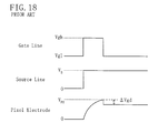
- FIG. 18 shows a relationship among signal patterns which are applied to a gate line, a source line and a pixel electrode, respectively.
- a potential Vgh is applied to a gate line
- a TFT connected to the gate line is turned on, and a potential V S which has been applied to a source line connected to the TFT is applied via a drain electrode to a pixel electrode.
- writing is performed until a potential V P0 of the pixel electrode reaches the same as the potential V S of the source line.
- a potential Vgl is applied to the gate line, the potential of the pixel electrode drops, which results in a difference ⁇ Vgd from the potential V P0 upon completion of the writing.
- the difference ⁇ Vgd resulting from the drop of the potential of the pixel electrode is generated by a parasitic capacitance between a drain electrode and a gate electrode in each pixel, and is called a feedthrough voltage.
- the feedthrough voltage ⁇ Vgd varies from one pixel to another, display defects, such as brightness unevenness and flicker, are likely to be visually recognized.
- Vgpp represents a difference between Vgh and Vgl (Vgh - Vgl)
- Cgd represents a parasitic capacitance between a gate electrode and a drain electrode
- Cs represents an auxiliary capacitance
- Clc represents a liquid crystal capacitance.
- a resist on a glass substrate is exposed in a divided manner using a plurality of shots, and therefore exposure with relatively high alignment accuracy is required among a plurality of blocks defined for the corresponding areas on the glass substrate which are exposed in the shots.
- arrangement relationships among lines, electrodes and a semiconductor layer and the like differ from one block to another, and therefore the parasitic capacitance Cgd, which is determined by the overlapping area of the gate electrode and the drain electrode, differs from one block to another.
- the parasitic capacitance Cgd which is determined by the overlapping area of the gate electrode and the drain electrode
- widths of portions of a semiconductor layer in a TFT and a drain electrode overlapping the semiconductor layer which cross an end of a gate electrode are made smaller than the width of the drain electrode which is a channel width of the TFT. This can decrease the difference among blocks in the overlapping area between the gate electrode and the drain electrode which is caused by an alignment error in a direction perpendicular to the channel width.
- the present invention has been made in view of such issues, and an object of the invention is to suppress variations of a feedthrough voltage generated by a parasitic capacitance between a gate electrode and a drain electrode.
- a side end on one side in a direction in which the drain electrode crosses an end of the gate electrode so as to enter from the outside of the gate electrode to the inside thereof is disposed inside of the auxiliary capacitance line
- a side end on the other side in a direction in which the drain electrode crosses the end of the gate electrode so as to go out from the inside of the gate electrode to the outside thereof is disposed outside of the auxiliary capacitance line.
- an active matrix substrate of the invention comprising a plurality of pixel regions defined in a matrix form, a plurality of source lines provided to extend in parallel to one another between the pixel regions, a plurality of gate lines provided to extend in parallel to one another in directions intersecting the source lines, a plurality of auxiliary capacitance lines provided to each extend between the gate lines, a plurality of thin film transistors each having a gate electrode electrically connected to one of the gate lines, a semiconductor layer provided to overlap the gate electrode, a source electrode provided to overlap the gate electrode and the semiconductor layer, the source electrode being electrically connected to one of the source lines, and a drain electrode provided to cross an end of the gate electrode so as to overlap the gate electrode and the semiconductor layer, and a plurality of auxiliary capacitance electrodes provided in the corresponding pixel regions so as to extend along the auxiliary capacitance lines and to overlap the auxiliary capacitance lines, in the same layer as the drain electrode of each of the thin film transistors, wherein, in each of the auxiliary capacitance
- a side end on one side in a direction in which the drain electrode crosses an end of the gate electrode so as to enter from the outside of the gate electrode to the inside thereof is disposed inside of the auxiliary capacitance line
- a side end on the other side in a direction in which the drain electrode crosses the end of the gate electrode so as to go out from the inside of the gate electrode to the outside thereof is disposed outside of the auxiliary capacitance line.
- the auxiliary capacitance electrode in cases where the drain electrode deviates toward a side of the direction in which the drain electrode crosses the end of the gate electrode so as to enter from the outside of the gate electrode to the inside thereof, which results in an increase in the overlapping area of the drain electrode and the gate electrode, the auxiliary capacitance electrode also deviates toward the side of the same direction as the drain electrode, which causes the overlapping area of the auxiliary capacitance electrode and the auxiliary capacitance line to be increased by the amount corresponding to the deviation of the drain electrode.
- the auxiliary capacitance electrode also deviates toward the side of the same direction as the drain electrode, which causes the overlapping area of the auxiliary capacitance electrode and the auxiliary capacitance line to be decreased by the amount corresponding to the deviation of the drain electrode.
- an auxiliary capacitance between the auxiliary capacitance electrode and the auxiliary capacitance line can be increased and decreased in accordance with an increase and a decrease of a parasitic capacitance between the gate electrode and the drain electrode, effects of the parasitic capacitance and the auxiliary capacitance on a feedthrough voltage cancel each other. As a result, variations of the feedthrough voltage, which is generated by a parasitic capacitance between the gate electrode and the drain electrode, are suppressed.
- each of the auxiliary capacitance lines have a capacitance main line provided to extend along one of the gate lines, and a capacitance branch line provided to project to a side from the capacitance main line, and that each of the auxiliary capacitance electrodes be provided to overlap the capacitance main line and the capacitance branch line.
- each of the auxiliary capacitance electrodes is provided to overlap both the capacitance main line and the capacitance branch line, the overlapping area of the auxiliary capacitance electrode and the auxiliary capacitance line increases, which results in an increase in auxiliary capacitance to decrease the feedthrough voltage.
- the auxiliary capacitance electrode by lengthening, in the auxiliary capacitance electrode, a portion which crosses the side end of the auxiliary capacitance line, it becomes possible to increase the auxiliary capacitance in accordance with an increase and a decrease in parasitic capacitance between the gate electrode and the drain electrode. This enables an increase and a decrease of the auxiliary capacitance with respect to an increase and a decrease in parasitic capacitance between the gate electrode and the drain electrode to be appropriately adjusted, so that variations of the feedthrough voltage are suppressed as much as possible.
- the plurality of pixel regions be included in a plurality of pixel region groups arranged along the source lines, and that, in each of the pixel region groups, the source electrodes be connected to the same one of the source lines, and the gate electrodes are connected to the gate lines which differ from one another.
- the source electrodes are connected to the same source line, and the gate electrodes are connected to the gate lines which differ from one another. Therefore, the number of source lines connected to the source electrodes of each pixel region group can be made smaller than that in cases where, in each pixel region group, the source electrodes are connected to the source lines which differ from one another, and the gate electrodes are connected to the same gate line. This enables the number of source driver IC chips, which are more expensive than gate driver IC chips, to be decreased, and therefore cost can be reduced.
- a liquid crystal display device comprises the active matrix substrate, a counter substrate disposed to face the active matrix substrate, and a liquid crystal layer provided between the active matrix substrate and the counter substrate.
- inclusion of the active matrix substrate causes an auxiliary capacitance between the auxiliary capacitance electrode and the auxiliary capacitance line to be increased and decreased in accordance with an increase and a decrease of a parasitic capacitance between the gate electrode and the drain electrode.
- variations of a feedthrough voltage generated by the parasitic capacitance between the gate electrode and the drain electrodes are suppressed. This makes it difficult for brightness irregularities to be visually recognized on a display screen.
- a vertical alignment layer and a plurality of alignment regulating portions for dividing the liquid crystal layer into a plurality of domains for each of the pixel regions be provided on each of sides of the liquid crystal layer of the active matrix substrate and the counter substrate, and that at least part of the plurality of alignment regulating portions be formed to overlap at least one of the auxiliary capacitance lines and the auxiliary capacitance electrodes.
- the vertical alignment layer and the plurality of alignment regulating portions for dividing the liquid crystal layer into a plurality of domains for each pixel region are provided on each of the sides of the liquid crystal layer of the active matrix substrate and the counter substrate, and therefore, when a voltage is not applied to the liquid crystal layer, just liquid crystal molecules near the alignment regulating portions are aligned in a tilted manner centered at the alignment regulating portions, and all other liquid crystal molecules apart from the alignment regulating portions are aligned perpendicular to the surface of the active matrix substrate (counter substrate).
- a voltage is applied to the liquid crystal layer, liquid crystal molecules apart from the alignment regulating portions are aligned in accordance with the tilted alignment of the liquid crystal molecules near the alignment regulating portions. This suppresses the amount of transmitted light which varies with the angle of visual recognition, thereby improving visual angle characteristics during displaying an image. This improvement increases the viewing angle.
- the alignment regulating portions In areas where the alignment regulating portions are provided, the alignment of liquid crystal molecules is likely to be out of order, and therefore light transmittance is likely to decrease and light leakage is likely to occur. In areas where the auxiliary capacitance line and the auxiliary capacitance electrode are provided, the auxiliary capacitance line and the auxiliary capacitance electrode block light transmission to decrease the light transmittance. With the above configuration, at least part of the plurality of alignment regulating portions is formed to overlap at least one of the auxiliary capacitance line and the auxiliary capacitance electrode.
- the plurality of alignment regulating portions is formed so as not to overlap either the auxiliary capacitance lines or the auxiliary capacitance electrodes, the decrease in light transmittance is suppressed, and light leakage is suppressed from the areas where liquid crystal molecules are likely to be out of alignment, which results in an increase in contrast.
- each of the auxiliary capacitance lines have a capacitance main line provided to extend along one of the gate lines, and a capacitance branch line provided to project to a side from the capacitance main line, and that each of the auxiliary capacitance electrodes be provided to overlap the capacitance main line and the capacitance branch line.
- each auxiliary capacitance electrode is provided to overlap both the capacitance main line and the capacitance branch line, and therefore the overlapping area of the auxiliary capacitance electrode and the auxiliary capacitance line increases, which results in an increase in auxiliary capacitance to decrease the feedthrough voltage.
- the auxiliary capacitance electrode by lengthening, in the auxiliary capacitance electrode, a portion which crosses a side end of the auxiliary capacitance line, it becomes possible to increase the auxiliary capacitance which increases and decreases in accordance with an increase and a decrease in parasitic capacitance between the gate electrode and the drain electrode. This enables an increase and a decrease of the auxiliary capacitance with respect to an increase and a decrease in parasitic capacitance between the gate electrode and the drain electrode to be appropriately adjusted, so that variations of the feedthrough voltage are suppressed as much as possible.
- each of the auxiliary capacitance electrodes be provided to extend along the capacitance main line and the capacitance branch line such that, in a plurality of portions among portions along the capacitance main line and the capacitance branch line, the side end on one side is disposed inside of the auxiliary capacitance line, and the side end on another side is disposed outside of the auxiliary capacitance line.
- auxiliary capacitance which increases and decreases in accordance with an increase and a decrease in parasitic capacitance between the gate electrode and the drain electrode, more than the case in which, in just one portion among portions along the capacitance main line and the capacitance branch lines of the auxiliary capacitance electrode, a side end on the one side is disposed inside of the auxiliary capacitance line, and a side end on the other side is disposed outside of the auxiliary capacitance line.
- a pixel electrode electrically connected to the drain electrode may be provided in each of the pixel regions, each of the alignment regulating portions of the active matrix substrate may be made of a slit formed in the pixel electrode, and each of the alignment regulating portions of the counter substrate may be made of a projection formed to project on the side of the liquid crystal layer.
- a pixel electrode electrically connected to the drain electrode may be provided in each of the pixel regions, a common electrode may be provided to overlap the pixel electrode, on the side of the liquid crystal layer of the counter substrate, each of the alignment regulating portions of the active matrix substrate may be made of a slit formed in the pixel electrode, and each of the alignment regulating portions of the counter substrate may be made of a slit formed in the common electrode.
- a side end on one side in a direction in which the drain electrode crosses an end of the gate electrode so as to enter from the outside of the gate electrode to the inside thereof is disposed inside of the auxiliary capacitance line
- a side end on the other side in a direction in which the drain electrode crosses the end of the gate electrode so as to go out from the inside of the gate electrode to the outside thereof is disposed outside of the auxiliary capacitance line
- FIGS. 1 to 8 show a first embodiment of the invention.
- FIG. 1 is a plan view schematically showing a liquid crystal display device S.
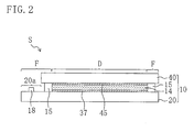
- FIG. 2 is a cross-sectional view schematically showing the liquid crystal display device S, taken along the line II-II of FIG. 1 .
- FIG. 3 is a plan view schematically showing, on an enlarged scale, part of the liquid crystal display device S.
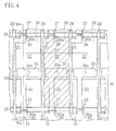
- FIG. 4 is a plan view schematically showing, on an enlarged scale, part of one substrate 20 included in the liquid crystal display device S.
- FIG. 5 is a cross-sectional view schematically showing the liquid crystal display device S, taken along the line V-V of FIG. 3 . Note that, in FIG. 4 , a laminated insulating film 35 and pixel electrodes 36 are shown transparent.
- the liquid crystal display device S includes a liquid crystal display panel 10 in which a pair of substrates 20 and 40 are bonded together.
- the liquid crystal display panel 10 includes the active matrix substrate 20, the counter substrate 40 disposed to face the active matrix substrate 20, and a liquid crystal layer 14 provided between the active matrix substrate 20 and the counter substrate 40.
- the liquid crystal display panel 10 has a display portion D in which an image is displayed, and a frame portion F which is a non-display portion disposed outside of the display portion D.
- the active matrix substrate 20 and the counter substrate 40 are formed, for example, in rectangular forms. As shown in FIG. 2 , alignment layers 37 and 45 are provided on the surfaces on the sides of the liquid crystal layer 14 of the active matrix substrate 20 and the counter substrate 40, respectively, and polarizing plates (not shown) are provided on the surfaces on the sides remote from the liquid crystal layer 14 of the active matrix substrate 20 and the counter substrate 40, respectively.
- a sealing material 15 in a frame form made of an epoxy resin is disposed between the active matrix substrate 20 and the counter substrate 40, and a liquid crystal material is enclosed inside of the sealing material 15, so that the liquid crystal layer 14 is provided.
- the display portion D includes a plurality of pixels 11 provided in a matrix form.
- each plurality of pixels 11 arranged in the row direction are included in a pixel group 12.
- the minimum unit of image display is referred to as a "pixel,” and one "pixel group” includes "pixels" of a plurality of colors.
- each pixel group 12 in the present embodiment includes red, green and blue pixels 11r, 11g and 11b arranged in the form of stripes in the row direction.
- Each pixel 11 is provided such that the length in the column direction (the longitudinal direction in FIG. 3 ) is approximately three times the length in the row direction.
- the counter substrate 40 is provided with a black matrix 43 to be described later, and therefore regions in which openings of the black matrix 43 are formed correspond to the pixels 11.
- a plurality of pixel regions 22 included in the corresponding pixels 11 are defined in a matrix form. That is, each pixel 11 is configured such that the corresponding pixel region 22 and the counter substrate 40 face each other with the liquid crystal layer 14 interposed therebetween.
- the plurality of pixel regions 22 are included in a plurality of pixel region groups 23 such that a plurality of pixel regions 22 arranged in the row direction so as to correspond to one pixel group 12 are included in each pixel region group 23.
- the active matrix substrate 20 has a glass substrate 21 shown in FIG. 5 , and includes, in the display portion D on the glass substrate 21, as shown in FIG. 4 , a plurality of source lines 24 provided to extend in parallel to one another between the pixel regions 22, a plurality of gate lines 25 provided to extend in parallel to one another in the directions intersecting the source lines 24 between the pixel regions 22, a plurality of thin film transistors (hereinafter referred to as "TFT") 27 electrically connected to the corresponding source lines 24 and gate lines 25, and a plurality of pixel electrodes 36 electrically connected to the corresponding TFT 27.
- TFT thin film transistors
- Each source line 24 is linearly provided to extend in the column direction, and each gate line 25 is linearly provided to extend in the row direction.
- Each auxiliary capacitance line 26 is linearly provided between the gate lines 25 to extend along the gate lines 25.
- Each TFT 27 is provided near an intersection of the source line 24 and the gate line 25 for the corresponding pixel region 22.
- the TFTs 27 in each pixel region group 23 are connected to the source lines 24 which differ from one another, and are connected to the same gate line 25.
- Each TFT 27, as shown in FIG. 5 is a bottom gate TFT, and includes a gate electrode 28 electrically connected to the gate line 25, a semiconductor layer 30 provided to overlap the gate electrode 28, a source electrode 31 connected to the semiconductor layer 30 on one side of the gate electrode 28, and a drain electrode 32 connected to the semiconductor layer 30 on the other side of the gate electrode 28.
- the gate lines 25, as shown in the drawing, are formed together with the auxiliary capacitance lines 26 on the surface of the glass substrate 21 and are covered with the gate insulating film 29.
- the semiconductor layer 30 of each TFT 27 is formed to cross part of the gate line 25 with the gate insulating film 29 interposed therebetween. Part of the gate line 25 overlapping the semiconductor layer 30 forms the gate electrode 28 of the TFT 27.
- Each semiconductor layer 30, which is not shown, includes, for example, an intrinsic amorphous silicon layer and n+ amorphous silicon layer laminated in sequence.
- the n+ amorphous silicon layer, from which an area overlapping the gate electrode 28 is partially removed, is divided into two, and an area of the intrinsic amorphous silicon layer exposed from the n+ amorphous silicon layer forms a channel 30a.
- Each source electrode 31 is formed to cross one end of the gate electrode 28 in the width direction of the gate line 25 to overlap the gate electrode 28 and the semiconductor layer 30, and is connected to the corresponding source line 24 as shown in FIG. 4 .
- Each drain electrode 32 is formed apart from the source electrode 31 with the channel 30a sandwiched therebetween such that the drain electrode 32 crosses the other end of the gate electrode 28 so as to overlap the gate electrode 28 and the semiconductor layer 30.
- an auxiliary capacitance electrode 33 is provided in each pixel region 22 to extend along the auxiliary capacitance line 26 and to overlap the auxiliary capacitance line 26 such that, in each pixel region 22, an auxiliary capacitance for holding a potential written in the pixel electrode 36 is formed between the auxiliary capacitance line 26 and the auxiliary capacitance electrode 33.
- Each auxiliary capacitance electrode 33 is formed integrally with the drain electrode 32 of the TFT 27 in the pixel region 22 in which the auxiliary capacitance electrode 33 is provided.
- the auxiliary capacitance electrode 33 is configured, as shown in FIG. 4 , such that a side end on one side (lower side in the drawing) in a direction in which the drain electrode 32 crosses an end of the gate electrode 28 so as to enter from the outside of the gate electrode 28 to the inside thereof is disposed inside of the auxiliary capacitance line 26, and such that a side end on the other side (upper side in the drawing) in a direction in which the drain electrode 32 crosses the end of the gate electrode 28 so as to go out from the inside of the gate electrode 28 to the outside thereof is disposed outside of the auxiliary capacitance line 26.
- the auxiliary capacitance electrode 33 in each pixel region 22 is disposed so as to increase and decrease an auxiliary capacitance between the auxiliary capacitance line 26 and the auxiliary capacitance electrode 33 in accordance with an increase and a decrease of a parasitic capacitance between the gate electrode 28 and the drain electrode 32 caused by a deviation in the column direction (the longitudinal direction in FIG. 4 ) of the position at which the integrally formed drain electrode 32 is formed.
- the drain electrode 32 and the auxiliary capacitance electrode 33 be formed such that an increase and a decrease of the sum of an auxiliary capacitance between the auxiliary capacitance line 26 and the auxiliary capacitance electrode 33 and a liquid crystal capacitance agree with an increase and a decrease of the parasitic capacitance between the drain electrode 32 and the gate electrode 28 which are caused by the deviation of the position at which the drain electrode 32 is formed.
- each TFT 27 and the auxiliary capacitance electrodes 33 Laminated above each TFT 27 and the auxiliary capacitance electrodes 33 is the laminated insulating film 35, shown in FIG. 5 , in which a silicon nitride film and an acrylic resin film (both not shown) are sequentially laminated. On the surface of the laminated insulating film 35, the pixel electrodes 36 are formed.
- the pixel electrode 36 is formed in a rectangular form whose length in the column direction is approximately three times the length in the row direction, and is provided in each pixel region 22. Note that while each pixel electrode 36 is formed in a rectangular form in the present embodiment, each pixel electrode 36 may be formed in various forms, such as a form in which part of a rectangular electrode is cut away and a form in which part of the rectangular electrode projects.
- a plurality of contact holes 35a for establishing connection with the corresponding auxiliary capacitance electrodes 33 are formed in the laminated insulating film 35.
- the alignment of liquid crystal molecules is likely to be out of order near the contact holes 35a, and the contact holes 35a are formed to expose central portions of the corresponding auxiliary capacitance electrodes 33. This causes areas near the contact holes 35a to be shielded from light by the auxiliary capacitance lines 26 and the auxiliary capacitance electrodes 33, which suppresses decreases in contrast which are caused by light leakage.
- the auxiliary capacitance electrodes 33 are connected to the corresponding pixel electrodes 36, so that the drain electrodes 32 of each TFT 27 are electrically connected through the auxiliary capacitance electrodes 33 to the pixel electrodes 36.
- the active matrix substrate 20, as shown in FIG. 1 and FIG. 2 has, in the frame portion F, for example, a mounting portion 20a whose two adjacent sides project in the form of the letter L outside of the counter substrate 40.
- Mounted on one side (lower side in FIG. 1 ) of the mounting portion 20a are, for example, a plurality of gate driver IC (integrated circuit) chips 17 each of which a given number of gate lines 25 are connected to.
- a plurality of source driver IC chips 18 each of which a given number of source lines 24 are connected to.
- each of the sides of the mounting portion 20a are a plurality of flexible printed wiring boards (not shown) which are electrically connected to a group of gate driver IC chips 17 and a group of source driver IC chips 18 and which supply signals and power to the driver IC chips 17 and 18.
- the counter substrate 40 has a glass substrate 41.
- a plurality of color filters 42 whose colors correspond to colors of the pixels 11 are provided to overlap the corresponding pixel electrodes 36, and the black matrixes 43 are provided to partition the color filters 42.
- a common electrode 44 is formed to cover the color filters 42 and the black matrixes 43.
- the liquid crystal display device S is configured such that gate signals are supplied to the gate lines 25 to sequentially turn on each TFT 27, and source signals are supplied to the source lines 24 connected to the TFTs 27 in the ON state, so that potentials applied to the source electrodes 31 of the TFTs 27 is sequentially written in the corresponding pixel electrodes 36 to apply voltages to the liquid crystal layer 14 between the pixel electrodes 36 and the common electrodes 44 to control the alignment of liquid crystal molecules for every pixel 11 so as for a desired image to be displayed.
- the active matrix substrate 20 and the counter substrate 40 are individually fabricated, and the alignment layers 37 and 45 are formed on the substrates 20 and 40, respectively. Then, both the substrates 20 and 40 are bonded to each other by using the sealing material 15, and the liquid crystal layer 14 is enclosed between both the substrates 20 and 40 by using the sealing material 15.
- the liquid crystal display panel 10 is thus manufactured. After the polarizing plates are attached to both surfaces of the liquid crystal display panel 10, the driver IC chips 17 and 18 and the flexible printed wiring boards are mounted thereon.
- the liquid crystal display device S of the invention is particularly characterized by the structure of the active matrix substrate 20, and therefore a method of manufacturing the active matrix substrate 20 is described in detail below with reference to FIGS. 6 to 8.
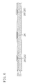
- FIGS. 6 to 8 are drawings for showing a method of manufacturing the active matrix substrate 20 and are cross-sectional views schematically showing an area corresponding to one pixel region 22 of the glass substrate 21.
- a metal film e.g., a thickness of about 50 to 500 nm
- aluminum is formed over the entire one surface of the glass substrate 21 by a sputtering method, and then patterning of the metal film is performed by photolithography, so that the gate lines 25 (the gate electrodes 28) and the auxiliary capacitance lines 26 are formed as shown in FIG. 6 .
- the exposure process of the step-division exposure method is performed although a description thereof is omitted.
- a silicon nitride film (e.g., a thickness of about 100 to 500 nm) or the like is formed over the entire surface on which the gate lines 25 (gate electrodes 28) and the auxiliary capacitance lines 26 are formed, by a plasma CVD (chemical vapor deposition) method, so that the gate insulating film 29 is formed.
- a plasma CVD chemical vapor deposition
- an intrinsic amorphous silicon film e.g., a thickness of about 50 to 100 nm
- an n+ amorphous silicon film e.g., a thickness of 50 to 100 nm
- an n-type impurity element such as phosphorus
- the semiconductor layers 30 may be formed of an amorphous silicon film as described above, but may be formed of a poly silicon film.
- a laser annealing process of an amorphous silicon film or a poly silicon film may be performed, so that the crystallinity improves.
- a metal film e.g., a thickness of about 50 to 500 nm
- a metal film e.g., a thickness of about 50 to 500 nm
- the metal film is patterned by photolithography, so that the source lines 24, the source electrodes 31, the drain electrodes 32 and the auxiliary capacitance electrodes 33 are formed.
- each TFT 27 is formed.
- a silicon nitride film e.g., a thickness of about 100 to 300 nm
- an acrylic resin film e.g., a thickness of about 1000 to 5000 nm
- a spin coating method so that the laminated insulating film 35 is formed.
- each auxiliary capacitance electrode 33 in the laminated insulating film 35 is removed by etching to form each contact hole 35a.
- a transparent conductive film e.g., a thickness of about 100 to 200 nm
- ITO indium tin oxide
- the transparent conductive film is patterned by photolithography, so that each pixel electrode 36 is formed.
- the active matrix substrate 20 is manufactured.
- the auxiliary capacitance electrode 33 is configured such that a side end on one side in a direction in which the drain electrode 32 crosses an end of the gate electrode 28 so as to enter from the outside of the gate electrode 28 to the inside thereof is disposed inside of the auxiliary capacitance line 26, and such that a side end on the other side in a direction in which the drain electrode 32 crosses the end of the gate electrode 28 so as to go out from the inside of the gate electrode 28 to the outside thereof is disposed outside of the auxiliary capacitance line 26.
- the auxiliary capacitance electrode 33 in which the drain electrode 32 crosses the end of the gate electrode 28 so as to enter from the outside of the gate electrode 28 to the inside thereof, which results in an increase in the overlapping area of the drain electrode 32 and the gate electrode 28, the auxiliary capacitance electrode 33 also deviates toward the side of the same direction as the drain electrode 32, which allows the overlapping area of the auxiliary capacitance electrode 33 and the auxiliary capacitance line 26 to be increased by the amount corresponding to the deviation of the drain electrode 32.
- the drain electrode 32 deviates toward a side of the direction (upper side in FIG.
- the drain electrode 32 crosses the end of the gate electrode 28 so as to go out from the inside of the gate electrode 28 to the outside thereof, which results in a decrease in the overlapping area of the drain electrode 32 and the gate electrode 28, the auxiliary capacitance electrode 33 also deviates toward the side of the same direction as the drain electrode 32, which allows the overlapping area of the auxiliary capacitance electrode 33 and the auxiliary capacitance line 26 to be decreased by the amount corresponding to the deviation of the drain electrode 32.
- an auxiliary capacitance between the auxiliary capacitance electrode 33 and the auxiliary capacitance line 26 can be increased and decreased in accordance with an increase and a decrease of a parasitic capacitance between the gate electrode 28 and the drain electrode 32, effects of the parasitic capacitance and the auxiliary capacitance on the feedthrough voltage cancel each other.
- lines 24, 25 and 26 and electrodes 28, 31, 32 and 33 are formed by photolithography including an exposure process of a step-division exposure method, the variation of the feedthrough voltage generated by the parasitic capacitance between the gate electrode 28 and the drain electrodes 32 can be suppressed among a plurality of blocks defined for areas on the glass substrate which are exposed in the corresponding shots. This makes it difficult for brightness irregularities among blocks to be visually recognized on a display screen.
- FIGS. 9 to 11 show the second embodiment of the invention. Note that, in the following embodiments, the same parts as those in FIGS. 1 to 8 are denoted by the same reference characters, and the detailed description thereof is omitted.
- FIG. 9 is a plan view schematically showing one pixel group 12 of the liquid crystal display device S of the present embodiment.
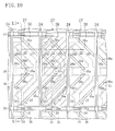
- FIG. 10 is a plan view schematically showing one pixel region group 23 of the active matrix substrate 20 of the present embodiment.
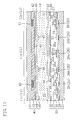
- FIG. 11 is a cross-sectional view schematically showing the liquid crystal display device S, taken along the line XI-XI of FIG. 9 .
- the liquid crystal display device S of the present embodiment is a liquid crystal display device of what is called MVA (multidomain vertical alignment) method.
- the liquid crystal layer 14 is made of a vertical alignment type nematic liquid crystal material having a negative dielectric anisotropy, and each of the alignment layers 37 and 45 is a vertical alignment layer.
- a plurality of alignment regulating portions 36a and 46 for dividing the liquid crystal layer 14 into a plurality of domains for each pixel region 22, that is, in each pixel 11 are provided, respectively.
- the alignment regulating portions 36a of the active matrix substrate 20, as shown in FIG. 10 and FIG. 11 are formed of slits of openings formed in each pixel electrode 36.
- the alignment regulating portions 46 of the counter substrate 40, as shown in FIG. 11 include projections formed to project toward the liquid crystal layer 14, and are provided between the common electrode 44 and the vertical alignment layer 45.
- the slits 36a and the projections 46 are linearly formed to extend in oblique directions with respect to the gate line 25 and the source line 24.
- the slits 36a and the projections 46 are, in the upper half region in FIG. 9 , each formed to extend from upper left to lower right in the drawing and are alternately arranged from upper right toward lower left in the drawing, whereas they are, in the lower half region in FIG. 9 , each formed to extend from upper right to lower left in the drawing and are alternately arranged from upper left toward lower right in the drawing.
- Each auxiliary capacitance line 26 of the active matrix substrate 20 of the present embodiment has a capacitance main line 26a provided to extend along the gate lines 25 and a plurality of capacitance branch lines 26b provided to project from the capacitance main line 26a to both sides thereof.
- the capacitance branch lines 26b are formed to overlap the corresponding projections 46, and are formed to extend in the oblique directions with respect to the corresponding source lines 24 and gate lines 25. That is, part of a plurality of projections 46 is formed to overlap the capacitance branch lines 26b. Note that while the capacitance branch lines 26b are shown thicker than the alignment regulating portions 36a and 46 in FIG. 9 and FIG. 10 , the capacitance branch lines 26b may be formed to have a thickness equal to those of the alignment regulating portions 36a and 46 or larger than those of the alignment regulating portions 36a and 46.
- the auxiliary capacitance electrodes 33 extend along the capacitance main line 26a and the capacitance branch lines 26b and are provided to overlap both the capacitance main line 26a and the capacitance branch lines 26b.
- the auxiliary capacitance electrode 33 is configured, just in one portion along the capacitance branch line 26b on the upper side in FIG. 10 among portions along the capacitance main line 26a and the capacitance branch lines 26b, such that a side end on one side (lower side in FIG.
- the auxiliary capacitance electrode 33 is configured such that the side end on one side in the direction in which the drain electrode 32 crosses the end of the gate electrode 28 so as to enter from the outside of the gate electrode 28 to the inside thereof is disposed inside of the auxiliary capacitance line 26, and such that the side end on the other side in the direction in which the drain electrode 32 crosses the end of the gate electrode 28 so as to go out from the inside of the gate electrode 28 to the outside thereof is disposed outside of the auxiliary capacitance line 26. Therefore, similar effects to those in the above the first embodiment can be obtained.
- the vertical alignment layers 37 and 45 and a plurality of alignment regulating portions 36a and 46 for dividing the liquid crystal layer 14 into a plurality of domains for each pixel 14 are provided on the sides of the liquid crystal layer 14 of the active matrix substrate 20 and the counter substrate 40, respectively, when a voltage is not applied to the liquid crystal layer 14, just liquid crystal molecules near the slits 36a and the projections 46 are aligned in a tilted manner centered at the slits 36a and the projections 46, and all other liquid crystal molecules apart from the slits 36a and the projections 46 are aligned perpendicular to the surface of the active matrix substrate 20 (counter substrate 40).
- liquid crystal molecules apart from the slits 36a and the projections 46 are aligned in accordance with the tilted alignment of the liquid crystal molecules near the slits 36a and the projections 46. This can suppress the amount of transmitted light which varies with the angle of visual recognition, thereby allowing improvement of visual angle characteristics during displaying an image. This improvement allows the viewing angle to increase.
- each auxiliary capacitance electrode 33 is provided to overlap both the capacitance main line 26a and the capacitance branch line 26b, the overlapping area of the auxiliary capacitance electrode 33 and the auxiliary capacitance line 26 becomes large, which results in an increase in auxiliary capacitance to decrease the feedthrough voltage.
- by lengthening a portion which crosses a side end of the auxiliary capacitance line 26 in the auxiliary capacitance electrode 33 it becomes possible to increase the auxiliary capacitance which increases and decreases in accordance with an increase and a decrease in parasitic capacitance between the gate electrode 28 and the drain electrode 32.
- the alignment regulating portions 36a and 46 are provided, the alignment of liquid crystal molecules is likely to be out of order, and therefore light transmittance is likely to decrease and light leakage is likely to occur.
- the auxiliary capacitance line 26 and the auxiliary capacitance electrode 33 block light transmission to decrease the light transmittance.
- part of the plurality of projections 46 is formed to overlap the corresponding capacitance branch lines 26b.
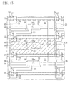
- FIG. 12 shows the third embodiment of the invention.
- FIG. 12 is a plan view schematically showing one pixel region group 23 of the active matrix substrate 20 of the present embodiment.
- the liquid crystal display device S in the present third embodiment is an MVA liquid crystal display device.
- a side end on one side in the direction in which the drain electrode 32 crosses the end of the gate electrode 28 so as to enter from the outside of the gate electrode 28 to the inside thereof is disposed inside of the auxiliary capacitance line 26, and a side end on the other side in the direction in which the drain electrode 32 crosses the end of the gate electrode 28 so as to go out from the inside of the gate electrode 28 to the outside thereof is disposed outside of the auxiliary capacitance line 26.
- each auxiliary capacitance electrode 33 in each auxiliary capacitance electrode 33, the side end on one side just in one portion along the capacitance branch line 26b on the upper side in FIG. 10 among portions along the capacitance main line 26a and the capacitance branch lines 26b is disposed inside of the auxiliary capacitance line 26, and the side end on the other side is disposed outside of the auxiliary capacitance line 26.
- the side end on the other side is disposed outside of the auxiliary capacitance line 26.
- side ends on the one side (lower side in the drawing) in a plurality of portions along the capacitance branch lines 26b on both sides in the upper and lower directions in the drawing are disposed along the side ends on one side of the capacitance branch lines 26b to be inside of the auxiliary capacitance line 26, and side ends of the other side (upper side in the drawing) are disposed along the side ends on the other side of the capacitance branch lines 26b to be outside of the auxiliary capacitance line 26.
- the auxiliary capacitance electrode 33 is configured such that the side end on one side in the direction in which the drain electrode 32 crosses the end of the gate electrode 28 so as to enter from the outside of the gate electrode 28 to the inside thereof is disposed inside of the auxiliary capacitance line 26, and such that the side end on the other side in the direction in which the drain electrode 32 crosses the end of the gate electrode 28 so as to go out from the inside of the gate electrode 28 to the outside thereof is disposed outside of the auxiliary capacitance line 26. Therefore, similar effects to those in the above first embodiment can be obtained.
- an increase and a decrease of the auxiliary capacitance with respect to an increase and a decrease in parasitic capacitance between the gate electrode 28 and the drain electrode 32 is appropriately adjusted, which enables variations of the feedthrough voltage to be suppressed as much as possible.
- FIG. 13 shows the fourth embodiment of the invention.
- FIG. 13 is a plan view schematically showing one pixel region 22 of the active matrix substrate 20 of the present embodiment.
- the liquid crystal display device S in the present embodiment is a liquid crystal display device of what is called PVA (patterned vertical alignment) method.
- the active matrix substrate 20 is configured in the same manner as the above second embodiment.
- the alignment regulating portions 36a and 44a of the active matrix substrate 20 and the counter substrate 40 are disposed in the same manner as the above second embodiment, and the alignment regulating portions 36a of the active matrix substrate 20 are made of slits formed in the corresponding pixel electrodes 36.
- Alignment regulating portions 44a of the counter substrate 40 as shown in FIG. 13 , are made of slits formed in the common electrode 44.
- the active matrix substrate 20 may be configured in the same manner as the above third embodiment.
- the active matrix substrate 20 is configured in the same manner as the above second embodiment, and therefore the effects similar to those of the above first embodiment can be obtained.
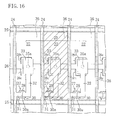
- FIGS. 14 and 15 show the fifth embodiment of the invention.
- FIG. 14 is a plan view schematically showing one pixel group 12 of the liquid crystal display device S in the present embodiment.
- FIG. 15 is a plan view schematically showing one pixel region group 23 of the active matrix substrate 20 in the present embodiment.
- a plurality of pixels 11 of the present embodiment are included in a plurality of pixel groups 12 such that the pixels 11r, 11g and 11b in a plurality of colors which are arranged in the form of stripes in the column direction and which are aligned along the source lines 24 are included in each pixel group 12.
- Each pixel 11 is provided such that the length in the row direction is approximately three times the length in the column direction.
- each TFT 27 in each pixel region group 23 are connected to the source lines 24 which are different from one another and are connected to the same gate line 25.
- each TFT 27 in each pixel region group 23 is configured such that the source electrodes 31 are connected to the same source line 24, and the gate electrodes 28 are connected to the gate lines 25 which differ from one another.
- the auxiliary capacitance electrode 33 is configured such that a side end on one side (lower side in FIG. 15 ) in a direction in which the drain electrode 32 crosses the end of the gate electrode 28 so as to enter from the outside of the gate electrode 28 to the inside thereof is disposed inside of the auxiliary capacitance line 26, and such that a side end on the other side (upper side in FIG. 15 ) in a direction in which the drain electrode 32 crosses the end of the gate electrode 28 so as to go out from the inside of the gate electrode 28 to the outside thereof is disposed outside of the auxiliary capacitance line 26.
- the auxiliary capacitance electrode 33 is configured such that the side end on one side in the direction in which the drain electrode 32 crosses the end of the gate electrode 28 so as to enter from the outside of the gate electrode 28 to the inside thereof is disposed inside of the auxiliary capacitance line 26, and such that the side end on the other side in the direction in which the drain electrode 32 crosses the end of the gate electrode 28 so as to go out from the inside of the gate electrode 28 to the outside thereof is disposed outside of the auxiliary capacitance line 26. Therefore, similar effects to those in the above first embodiment can be obtained.
- intervals 109 between the gate lines 101 and the auxiliary capacitance lines 105 are made smaller than those in cases where the length in the column direction in each pixel region is approximately three times the length in the row direction, from the viewpoint of fully shielding areas near the contact holes 103 of the laminated insulating film from light by the auxiliary capacitance lines 105. This causes the lines 101 and 105 to be easily short-circuited to each other, and therefore the yields tend to decrease.
- auxiliary capacitance electrode 33 on a side (upper side in the drawing) of the direction in which the drain electrode 32 crosses the end of the gate electrode 28 so as to go out from the inside of the gate electrode 28 to the outside thereof is disposed outside of the auxiliary capacitance line 26.
- each pixel region group 23 the source electrodes 31 are connected to the same source line 24, and the gate electrodes 28 are connected to the gate lines 25 which differ from one another. Therefore, the number of source lines 24 connected to the source electrode 31 of each pixel region group 23 can be made smaller than that in cases where, in each pixel region group 23, the source electrodes 31 are connected to the source lines 24 which differ from one another and the gate electrodes 28 are connected to the same gate line 25. This enables the number of source driver IC chips 18, which are more expensive than the gate driver IC chips 17, to be decreased, and therefore cost can be reduced.
- the auxiliary capacitance electrode 33 in each pixel region 22 is disposed such that the auxiliary capacitance between the auxiliary capacitance line 26 and the auxiliary capacitance electrode 33 increases and decreases in accordance with an increase and a decrease of the parasitic capacitance between the gate electrode 28 and the drain electrode 32 which are caused by the deviation in the column direction of the position at which the drain electrode 32 is integrally formed.
- the invention is not limited to this. As shown in FIG.
- the auxiliary capacitance electrode 33 in each pixel region 22 may be disposed such that the auxiliary capacitance between the auxiliary capacitance line 26 and the auxiliary capacitance electrode 33 increases and decreases in accordance with an increase and a decrease of the parasitic capacitance between the gate electrode 28 and the drain electrode 32 which are caused by the deviation in the row direction (the lateral direction in the drawing) of the position at which the drain electrode 32 is integrally formed.
- each gate electrode 28 is provided to project from the gate line 25 on a side of the auxiliary capacitance line 26 (upper side in the drawing), each semiconductor layer 30 is provided to overlap the gate electrode 28, and, in each pixel region 22, a side end on one side (left side in the drawing) of the drain electrode 32 is disposed inside of the semiconductor layer 30, and a side end on the other side (right side in the drawing) is disposed outside of the semiconductor layer 30.
- a swell 26c which swells in the column direction is provided in a portion overlapping the auxiliary capacitance electrode 33.
- the auxiliary capacitance electrode 33 may be configured such that a side end on one side (left side in FIG.
- auxiliary capacitance between the auxiliary capacitance electrode 33 and the auxiliary capacitance line 26 can be increased and decreased in accordance with an increase and a decrease of the parasitic capacitance between the gate electrode 28 and the drain electrode 32, effects of the parasitic capacitance and the auxiliary capacitance on the feedthrough voltage cancel each other. As a result, it becomes possible to suppress variations of the feedthrough voltage generated by the parasitic capacitance between the gate electrode 28 and the drain electrode 32.
- the drain electrodes 32 and the corresponding auxiliary capacitance electrodes 33 are integrally formed.
- the invention is not limited to this, and the drain electrodes and the auxiliary capacitance electrodes may be separately formed.
- an active matrix substrate is configured, for example, such that contact holes which pass through a laminated insulating film are formed on drain electrodes and auxiliary capacitance electrodes, and the drain electrodes and the auxiliary capacitance electrodes are connected through the contact holes to pixel electrodes, so that the drain electrodes and the auxiliary capacitance electrodes are electrically connected.
- the alignment regulating portions 36a of the active matrix substrate 20 are made of slits of openings which are formed in the corresponding pixel electrodes 36, and the alignment regulating portions 46 of the counter substrate 40 are made of projections.
- the invention is not limited to this, and the alignment regulating portions of the active matrix substrate 20 may be made of projections which are formed to project on the side of the liquid crystal layer 14, and alignment regulating portions of the counter substrate 40 may be made of slits of openings which are formed in the common electrode 44.
- the slits of the active matrix substrate 20 may be made of cutouts. Even with such a configuration, it becomes possible to obtain effects similar to those in the above second embodiment.
- the capacitance branch lines 26b are formed to overlap the projections 46.
- the capacitance branch lines 26b may be formed to overlap the slits 36a, and part of the slits 36a may be formed to overlap the capacitance branch lines 26b. It is preferable that at least part of a plurality of alignment regulating portions 36a and 46 be formed to overlap at least part of the auxiliary capacitance lines 26 and the auxiliary capacitance electrodes 33.
- part of a plurality of alignment regulating portions 36a and 46 near which alignment of liquid crystal molecules is likely to be out of order is formed to overlap at least part of the auxiliary capacitance line 26 and the auxiliary capacitance electrode 33 which block light transmission. It is therefore possible to suppress the decrease in light transmittance, and suppress light leakage from the areas where liquid crystal molecules are likely to be out of alignment, which enables contrast to be increased, compared to cases where part of the plurality of alignment regulating portions 36a and 46 is formed in another area, that is, the plurality of alignment regulating portions 36a and 46 are formed so as not to overlap either the auxiliary capacitance line 26 or the auxiliary capacitance electrode 33.
- FIG. 15 shows one linearly formed auxiliary capacitance line 26.
- each auxiliary capacitance line 26 may have a capacitance main line provided to extend along the gate line 25 and a capacitance branch line provided to project to a side from the capacitance main line, as in the above second embodiment, and further the auxiliary capacitance electrode 33 may be provided to overlap the capacitance main line and the capacitance branch line.
- liquid crystal display device S to which the active matrix substrate 20 is applied.
- the invention is not limited to this, and is applicable to other display devices, such as organic electroluminescent display devices.
- the invention is useful for an active matrix substrate and a liquid crystal display device, and more particularly is suitable for an active matrix substrate and a liquid crystal display device in which there is a need for suppressing variations of a feedthrough voltage generated by a parasitic capacitance between a gate electrode and a drain electrode.
Landscapes
- Physics & Mathematics (AREA)
- Engineering & Computer Science (AREA)
- Nonlinear Science (AREA)
- Power Engineering (AREA)
- Microelectronics & Electronic Packaging (AREA)
- Mathematical Physics (AREA)
- Chemical & Material Sciences (AREA)
- Crystallography & Structural Chemistry (AREA)
- General Physics & Mathematics (AREA)
- Optics & Photonics (AREA)
- Liquid Crystal (AREA)
- Devices For Indicating Variable Information By Combining Individual Elements (AREA)
Abstract
Description
- The present invention relates to an active matrix substrate and a liquid crystal display device.
- Liquid crystal displays have characteristics that they are thin and that they require low power consumption. Making use of these characteristics leads to wide use of liquid crystal display devices, liquid crystal displays have conventionally been used in a wide range as displays of the whole devices which are not limited to common devices, such as television sets and personal computers, but include measurement hardware, medical equipment and industrial equipment. As the liquid crystal display device, an active matrix drive liquid crystal display device is known in which a TFT (thin film transistor) is provided for each pixel, that is the minimum unit for displaying an image, so as to allow a fine image to be displayed.
- The active matrix drive liquid crystal display device comprises an active matrix substrate on which a plurality of TFTs mentioned above are provided, a counter substrate which is disposed to face the active matrix substrate and on which a common electrode and the like are formed, and a liquid crystal layer provided between the active matrix substrate and the counter substrate.
-
FIG. 17 is a plan view schematically showing part of a conventional active matrix substrate. - In the active matrix substrate, as shown in
FIG. 17 , a plurality ofsource lines 100 extending in parallel to one another and a plurality ofgate lines 101 extending in parallel to one another are provided to intersect. On the active matrix substrate, eachTFT 102 is provided near the corresponding intersection of thesource line 100 and thegate line 101, and a plurality of pixel electrodes 104 (shown in a transmission form) which are electrically connected to thecorresponding TFT 102 throughcontact holes 103 formed in an insulating film (not shown) covering theTFTs 102 is formed in a matrix form. - Further, on the active matrix substrate, a plurality of
auxiliary capacitance lines 105 are provided to each extend between thegate lines 101. Provided on eachauxiliary capacitance line 105 are a plurality ofauxiliary capacitance electrodes 107 formed to be integrated withdrain electrodes 106 of thecorresponding TFTs 102, and auxiliary capacitances for holding potentials written in thecorresponding pixel electrodes 104 are formed between theauxiliary capacitance line 105 and theauxiliary capacitance electrodes 107 which overlap each other. -
FIG. 18 shows a relationship among signal patterns which are applied to a gate line, a source line and a pixel electrode, respectively. As shown inFIG. 18 , when a potential Vgh is applied to a gate line, a TFT connected to the gate line is turned on, and a potential VS which has been applied to a source line connected to the TFT is applied via a drain electrode to a pixel electrode. At this point, writing is performed until a potential VP0 of the pixel electrode reaches the same as the potential VS of the source line. When a potential Vgl is applied to the gate line, the potential of the pixel electrode drops, which results in a difference ΔVgd from the potential VP0 upon completion of the writing. The difference ΔVgd resulting from the drop of the potential of the pixel electrode is generated by a parasitic capacitance between a drain electrode and a gate electrode in each pixel, and is called a feedthrough voltage. In cases where the feedthrough voltage ΔVgd varies from one pixel to another, display defects, such as brightness unevenness and flicker, are likely to be visually recognized. - The feedthrough voltage ΔVgd is simply expressed by the following equation. Note that Vgpp represents a difference between Vgh and Vgl (Vgh - Vgl), Cgd represents a parasitic capacitance between a gate electrode and a drain electrode, Cs represents an auxiliary capacitance, and Clc represents a liquid crystal capacitance.

- In recent years, as upsizing of display screens of television sets and the like have been demanded, the sizes of active matrix substrates have become larger. To manufacture an active matrix substrate, pattern formation is usually performed using photolithography to form lines and electrodes. In photolithography at the time of manufacturing a large-sized active matrix substrate, performed as an exposure process in which a resist applied onto a glass substrate is exposed through a photomask is an exposure process of a step-division exposure method. In the exposure process of this method, a photomask smaller than a glass substrate is disposed on the glass substrate, and exposure is performed in a divided manner using a plurality of shots while the glass substrate is moved stepwise and the photomask is replaced as necessary.
- In the exposure process of the step-division exposure method, a resist on a glass substrate is exposed in a divided manner using a plurality of shots, and therefore exposure with relatively high alignment accuracy is required among a plurality of blocks defined for the corresponding areas on the glass substrate which are exposed in the shots. If an alignment error of an exposure device occurs in each block, arrangement relationships among lines, electrodes and a semiconductor layer and the like differ from one block to another, and therefore the parasitic capacitance Cgd, which is determined by the overlapping area of the gate electrode and the drain electrode, differs from one block to another. As a result, there is a difference in feedthrough voltage from one block to another, which makes it easy for brightness irregularities among blocks to be visually recognized on a display screen.
- In a liquid crystal display device disclosed in
PATENT DOCUMENT 1, widths of portions of a semiconductor layer in a TFT and a drain electrode overlapping the semiconductor layer which cross an end of a gate electrode are made smaller than the width of the drain electrode which is a channel width of the TFT. This can decrease the difference among blocks in the overlapping area between the gate electrode and the drain electrode which is caused by an alignment error in a direction perpendicular to the channel width. -
- PATENT DOCUMENT
PATENT DOCUMENT 1: Japanese Patent No.3881160 - However, even with a liquid crystal display device of
PATENT DOCUMENT 1, an alignment error of an exposure device occurs among blocks in the exposure process at the time of forming the drain electrode, both the arrangement relationship between the auxiliary capacitance electrode formed to be integrated with the drain electrode and the auxiliary capacitance line and the arrangement relationship between the gate electrode and the drain electrode differ from one block to another, and therefore the auxiliary capacitance Cs, which is determined by the overlapping area of the auxiliary capacitance electrode and the auxiliary capacitance line, varies from one block to another. As a result, both variations of the parasitic capacitance Cgd and variations of the auxiliary capacitance Cs occur among blocks. There is therefore a possibility that these two factors together prevent differences in the feedthrough voltage ΔVgd among blocks from being fully suppressed, which results in brightness irregularities being visually recognized on a display screen as described above. Thus, this liquid crystal display device has room for improvement. - The present invention has been made in view of such issues, and an object of the invention is to suppress variations of a feedthrough voltage generated by a parasitic capacitance between a gate electrode and a drain electrode.
- To achieve the above object, according to this invention, in each of auxiliary capacitance electrodes in the corresponding pixel regions, a side end on one side in a direction in which the drain electrode crosses an end of the gate electrode so as to enter from the outside of the gate electrode to the inside thereof is disposed inside of the auxiliary capacitance line, and a side end on the other side in a direction in which the drain electrode crosses the end of the gate electrode so as to go out from the inside of the gate electrode to the outside thereof is disposed outside of the auxiliary capacitance line.
- Specifically, an active matrix substrate of the invention comprising a plurality of pixel regions defined in a matrix form, a plurality of source lines provided to extend in parallel to one another between the pixel regions, a plurality of gate lines provided to extend in parallel to one another in directions intersecting the source lines, a plurality of auxiliary capacitance lines provided to each extend between the gate lines, a plurality of thin film transistors each having a gate electrode electrically connected to one of the gate lines, a semiconductor layer provided to overlap the gate electrode, a source electrode provided to overlap the gate electrode and the semiconductor layer, the source electrode being electrically connected to one of the source lines, and a drain electrode provided to cross an end of the gate electrode so as to overlap the gate electrode and the semiconductor layer, and a plurality of auxiliary capacitance electrodes provided in the corresponding pixel regions so as to extend along the auxiliary capacitance lines and to overlap the auxiliary capacitance lines, in the same layer as the drain electrode of each of the thin film transistors, wherein, in each of the auxiliary capacitance electrodes of the pixel regions, a side end on one side is disposed inside of one of the auxiliary capacitance lines, the side end on one side being in a direction in which the drain electrode crosses the end of the gate electrode so as to enter from outside of the gate electrode to inside thereof, and a side end on another side is disposed outside of the one of the auxiliary capacitance lines, the side end on another side being in a direction in which the drain electrode crosses the end of the gate electrode so as to go out from the inside of the gate electrode to the outside thereof.
- With this configuration, in the auxiliary capacitance electrode in each pixel region, a side end on one side in a direction in which the drain electrode crosses an end of the gate electrode so as to enter from the outside of the gate electrode to the inside thereof is disposed inside of the auxiliary capacitance line, and a side end on the other side in a direction in which the drain electrode crosses the end of the gate electrode so as to go out from the inside of the gate electrode to the outside thereof is disposed outside of the auxiliary capacitance line. This causes the overlapping area of the auxiliary capacitance electrode formed in the same layer as the drain electrode and the auxiliary capacitance line to vary in accordance with and together with the variation of the overlapping area of the gate electrode and the drain electrode. That is, in cases where the drain electrode deviates toward a side of the direction in which the drain electrode crosses the end of the gate electrode so as to enter from the outside of the gate electrode to the inside thereof, which results in an increase in the overlapping area of the drain electrode and the gate electrode, the auxiliary capacitance electrode also deviates toward the side of the same direction as the drain electrode, which causes the overlapping area of the auxiliary capacitance electrode and the auxiliary capacitance line to be increased by the amount corresponding to the deviation of the drain electrode. Alternatively, in cases where the drain electrode deviates toward a side of the direction in which the drain electrode crosses the end of the gate electrode so as to go out from the inside of the gate electrode to the outside thereof, which results in a decrease in the overlapping area of the drain electrode and the gate electrode, the auxiliary capacitance electrode also deviates toward the side of the same direction as the drain electrode, which causes the overlapping area of the auxiliary capacitance electrode and the auxiliary capacitance line to be decreased by the amount corresponding to the deviation of the drain electrode. Accordingly, since an auxiliary capacitance between the auxiliary capacitance electrode and the auxiliary capacitance line can be increased and decreased in accordance with an increase and a decrease of a parasitic capacitance between the gate electrode and the drain electrode, effects of the parasitic capacitance and the auxiliary capacitance on a feedthrough voltage cancel each other. As a result, variations of the feedthrough voltage, which is generated by a parasitic capacitance between the gate electrode and the drain electrode, are suppressed.
- It is preferable that each of the auxiliary capacitance lines have a capacitance main line provided to extend along one of the gate lines, and a capacitance branch line provided to project to a side from the capacitance main line, and that each of the auxiliary capacitance electrodes be provided to overlap the capacitance main line and the capacitance branch line.
- With this configuration, since each of the auxiliary capacitance electrodes is provided to overlap both the capacitance main line and the capacitance branch line, the overlapping area of the auxiliary capacitance electrode and the auxiliary capacitance line increases, which results in an increase in auxiliary capacitance to decrease the feedthrough voltage. In addition to this matter, by lengthening, in the auxiliary capacitance electrode, a portion which crosses the side end of the auxiliary capacitance line, it becomes possible to increase the auxiliary capacitance in accordance with an increase and a decrease in parasitic capacitance between the gate electrode and the drain electrode. This enables an increase and a decrease of the auxiliary capacitance with respect to an increase and a decrease in parasitic capacitance between the gate electrode and the drain electrode to be appropriately adjusted, so that variations of the feedthrough voltage are suppressed as much as possible.
- It is preferable that the plurality of pixel regions be included in a plurality of pixel region groups arranged along the source lines, and that, in each of the pixel region groups, the source electrodes be connected to the same one of the source lines, and the gate electrodes are connected to the gate lines which differ from one another.
- With this configuration, in each pixel region group, the source electrodes are connected to the same source line, and the gate electrodes are connected to the gate lines which differ from one another. Therefore, the number of source lines connected to the source electrodes of each pixel region group can be made smaller than that in cases where, in each pixel region group, the source electrodes are connected to the source lines which differ from one another, and the gate electrodes are connected to the same gate line. This enables the number of source driver IC chips, which are more expensive than gate driver IC chips, to be decreased, and therefore cost can be reduced.
- A liquid crystal display device according to the invention comprises the active matrix substrate, a counter substrate disposed to face the active matrix substrate, and a liquid crystal layer provided between the active matrix substrate and the counter substrate.
- With this configuration, inclusion of the active matrix substrate causes an auxiliary capacitance between the auxiliary capacitance electrode and the auxiliary capacitance line to be increased and decreased in accordance with an increase and a decrease of a parasitic capacitance between the gate electrode and the drain electrode. As a result, variations of a feedthrough voltage generated by the parasitic capacitance between the gate electrode and the drain electrodes are suppressed. This makes it difficult for brightness irregularities to be visually recognized on a display screen.
- It is preferable that a vertical alignment layer and a plurality of alignment regulating portions for dividing the liquid crystal layer into a plurality of domains for each of the pixel regions be provided on each of sides of the liquid crystal layer of the active matrix substrate and the counter substrate, and that at least part of the plurality of alignment regulating portions be formed to overlap at least one of the auxiliary capacitance lines and the auxiliary capacitance electrodes.
- With this configuration, the vertical alignment layer and the plurality of alignment regulating portions for dividing the liquid crystal layer into a plurality of domains for each pixel region are provided on each of the sides of the liquid crystal layer of the active matrix substrate and the counter substrate, and therefore, when a voltage is not applied to the liquid crystal layer, just liquid crystal molecules near the alignment regulating portions are aligned in a tilted manner centered at the alignment regulating portions, and all other liquid crystal molecules apart from the alignment regulating portions are aligned perpendicular to the surface of the active matrix substrate (counter substrate). When a voltage is applied to the liquid crystal layer, liquid crystal molecules apart from the alignment regulating portions are aligned in accordance with the tilted alignment of the liquid crystal molecules near the alignment regulating portions. This suppresses the amount of transmitted light which varies with the angle of visual recognition, thereby improving visual angle characteristics during displaying an image. This improvement increases the viewing angle.
- In areas where the alignment regulating portions are provided, the alignment of liquid crystal molecules is likely to be out of order, and therefore light transmittance is likely to decrease and light leakage is likely to occur. In areas where the auxiliary capacitance line and the auxiliary capacitance electrode are provided, the auxiliary capacitance line and the auxiliary capacitance electrode block light transmission to decrease the light transmittance. With the above configuration, at least part of the plurality of alignment regulating portions is formed to overlap at least one of the auxiliary capacitance line and the auxiliary capacitance electrode. Therefore, compared to cases where at least part of the plurality of alignment regulating portions is formed in another area, that is the plurality of alignment regulating portions is formed so as not to overlap either the auxiliary capacitance lines or the auxiliary capacitance electrodes, the decrease in light transmittance is suppressed, and light leakage is suppressed from the areas where liquid crystal molecules are likely to be out of alignment, which results in an increase in contrast.
- It is preferable that each of the auxiliary capacitance lines have a capacitance main line provided to extend along one of the gate lines, and a capacitance branch line provided to project to a side from the capacitance main line, and that each of the auxiliary capacitance electrodes be provided to overlap the capacitance main line and the capacitance branch line.
- With this configuration, each auxiliary capacitance electrode is provided to overlap both the capacitance main line and the capacitance branch line, and therefore the overlapping area of the auxiliary capacitance electrode and the auxiliary capacitance line increases, which results in an increase in auxiliary capacitance to decrease the feedthrough voltage. In addition to this matter, by lengthening, in the auxiliary capacitance electrode, a portion which crosses a side end of the auxiliary capacitance line, it becomes possible to increase the auxiliary capacitance which increases and decreases in accordance with an increase and a decrease in parasitic capacitance between the gate electrode and the drain electrode. This enables an increase and a decrease of the auxiliary capacitance with respect to an increase and a decrease in parasitic capacitance between the gate electrode and the drain electrode to be appropriately adjusted, so that variations of the feedthrough voltage are suppressed as much as possible.
- It is preferable that each of the auxiliary capacitance electrodes be provided to extend along the capacitance main line and the capacitance branch line such that, in a plurality of portions among portions along the capacitance main line and the capacitance branch line, the side end on one side is disposed inside of the auxiliary capacitance line, and the side end on another side is disposed outside of the auxiliary capacitance line.
- With this configuration, in a plurality of portions among portions along the capacitance main line and the capacitance branch lines in each auxiliary capacitance electrode, side ends on the one side are disposed inside of the auxiliary capacitance line, and side ends on the other side are disposed outside of the auxiliary capacitance line. This increases the auxiliary capacitance, which increases and decreases in accordance with an increase and a decrease in parasitic capacitance between the gate electrode and the drain electrode, more than the case in which, in just one portion among portions along the capacitance main line and the capacitance branch lines of the auxiliary capacitance electrode, a side end on the one side is disposed inside of the auxiliary capacitance line, and a side end on the other side is disposed outside of the auxiliary capacitance line.
- A pixel electrode electrically connected to the drain electrode may be provided in each of the pixel regions, each of the alignment regulating portions of the active matrix substrate may be made of a slit formed in the pixel electrode, and each of the alignment regulating portions of the counter substrate may be made of a projection formed to project on the side of the liquid crystal layer.
- With this configuration, when a voltage is not applied to the liquid crystal layer, just liquid crystal molecules near the slits and the projections are aligned in a tilted manner centered at the slits and the projections, and all other liquid crystal molecules apart from the slits and the projections are aligned perpendicular to the surface of the active matrix substrate (counter substrate). When a voltage is applied to the liquid crystal layer, liquid crystal molecules apart from the slits and the projections are aligned in accordance with the tilted alignment of the liquid crystal molecules near the slits and the projections. This suppresses the amount of transmitted light which varies with the angle of visual recognition, thereby improving visual angle characteristics during displaying an image. This improvement increases the viewing angle.
- A pixel electrode electrically connected to the drain electrode may be provided in each of the pixel regions, a common electrode may be provided to overlap the pixel electrode, on the side of the liquid crystal layer of the counter substrate, each of the alignment regulating portions of the active matrix substrate may be made of a slit formed in the pixel electrode, and each of the alignment regulating portions of the counter substrate may be made of a slit formed in the common electrode.
- With this configuration, when a voltage is not applied to the liquid crystal layer, just liquid crystal molecules near the slits of the pixel electrodes and the common electrode are aligned in a tilted manner centered at the slits, and all other liquid crystal molecules apart from the slits are aligned perpendicular to the surface of the active matrix substrate (the counter substrate). When a voltage is applied to the liquid crystal layer, liquid crystal molecules apart from the slits are aligned in accordance with the tilted alignment of the liquid crystal molecules near the slits. This suppresses the amount of transmitted light which varies with the angle of visual recognition, thereby improving visual angle characteristics during displaying an image. This improvement increases the viewing angle.
- According to the invention, in the auxiliary capacitance electrode in each pixel region, a side end on one side in a direction in which the drain electrode crosses an end of the gate electrode so as to enter from the outside of the gate electrode to the inside thereof is disposed inside of the auxiliary capacitance line, and a side end on the other side in a direction in which the drain electrode crosses the end of the gate electrode so as to go out from the inside of the gate electrode to the outside thereof is disposed outside of the auxiliary capacitance line, and therefore variations of the feedthrough voltage, which is generated by a parasitic capacitance between the gate electrode and the drain electrode, are suppressed.
-
- [
FIG. 1] FIG. 1 is a plan view schematically showing a liquid crystal display device. - [
FIG. 2] FIG. 2 is a schematic cross-sectional view taken along the line II-II ofFIG. 1 . - [
FIG. 3] FIG. 3 is a plan view schematically showing, on an enlarged scale, part of a liquid crystal display device in a first embodiment. - [
FIG. 4] FIG. 4 is a plan view schematically showing, on an enlarged scale, part of an active matrix substrate in the first embodiment. - [
FIG. 5] FIG. 5 is a schematic cross-sectional view taken along the line V-V ofFIG. 3 . - [
FIG. 6] FIG. 6 is a cross-sectional view schematically showing a glass substrate in a state in which a gate insulating film is formed. - [
FIG. 7] FIG. 7 is a cross-sectional view schematically showing the glass substrate in a state in which drain electrodes and an auxiliary capacitance electrode are formed. - [
FIG. 8] FIG. 8 is a cross-sectional view schematically showing the glass substrate in a state in which pixel electrodes are formed. - [
FIG. 9] FIG. 9 is a plan view schematically showing, on an enlarged scale, part of a display portion of a liquid crystal display device in a second embodiment. - [
FIG. 10] FIG. 10 is a plan view schematically showing, on an enlarged scale, part of an active matrix substrate in the second embodiment. - [
FIG. 11] FIG. 11 is a schematic cross-sectional view taken along the line XI-XI ofFIG. 9 . - [
FIG. 12] FIG. 12 is a plan view schematically showing, on an enlarged scale, part of an active matrix substrate in a third embodiment. - [
FIG. 13] FIG. 13 is a cross-sectional view schematically showing, on an enlarged scale, part of a display portion of a liquid crystal display device in a fourth embodiment. - [
FIG. 14] FIG. 14 is a plan view schematically showing, on an enlarged scale, part of a display portion of a liquid crystal display device in a fifth embodiment. - [
FIG. 15] FIG. 15 is a plan view schematically showing, on an enlarged scale, part of an active matrix substrate in the fifth embodiment. - [
FIG. 16] FIG. 16 is a plan view schematically showing, on an enlarged scale, part of an active matrix substrate in another embodiment. - [
FIG. 17] FIG. 17 is a plan view schematically showing, on an enlarged scale, part of a conventional active matrix substrate. - [
FIG. 18] FIG. 18 shows a relationship among signal patterns which are applied to a gate line, a source line and a pixel electrode, respectively. - [
FIG. 19] FIG. 19 is a plan view schematically showing, on an enlarged scale, part of a conventional active matrix substrate in which the length in the row direction in each pixel region is provided to be approximately three times the length in the column direction. - Embodiments of the invention will be described in detail below with reference to the drawings. Note that the invention is not limited to the following embodiments.
-
FIGS. 1 to 8 show a first embodiment of the invention.FIG. 1 is a plan view schematically showing a liquid crystal display device S.FIG. 2 is a cross-sectional view schematically showing the liquid crystal display device S, taken along the line II-II ofFIG. 1 .FIG. 3 is a plan view schematically showing, on an enlarged scale, part of the liquid crystal display device S.FIG. 4 is a plan view schematically showing, on an enlarged scale, part of onesubstrate 20 included in the liquid crystal display device S.FIG. 5 is a cross-sectional view schematically showing the liquid crystal display device S, taken along the line V-V ofFIG. 3 . Note that, inFIG. 4 , a laminated insulatingfilm 35 andpixel electrodes 36 are shown transparent. - The liquid crystal display device S, as shown in
FIG. 1 andFIG. 2 , includes a liquidcrystal display panel 10 in which a pair ofsubstrates crystal display panel 10 includes theactive matrix substrate 20, thecounter substrate 40 disposed to face theactive matrix substrate 20, and aliquid crystal layer 14 provided between theactive matrix substrate 20 and thecounter substrate 40. The liquidcrystal display panel 10 has a display portion D in which an image is displayed, and a frame portion F which is a non-display portion disposed outside of the display portion D. - The
active matrix substrate 20 and thecounter substrate 40 are formed, for example, in rectangular forms. As shown inFIG. 2 , alignment layers 37 and 45 are provided on the surfaces on the sides of theliquid crystal layer 14 of theactive matrix substrate 20 and thecounter substrate 40, respectively, and polarizing plates (not shown) are provided on the surfaces on the sides remote from theliquid crystal layer 14 of theactive matrix substrate 20 and thecounter substrate 40, respectively. A sealingmaterial 15 in a frame form made of an epoxy resin is disposed between theactive matrix substrate 20 and thecounter substrate 40, and a liquid crystal material is enclosed inside of the sealingmaterial 15, so that theliquid crystal layer 14 is provided. - The display portion D, as shown in
FIG. 3 , includes a plurality ofpixels 11 provided in a matrix form. Regarding the plurality ofpixels 11, each plurality ofpixels 11 arranged in the row direction (the lateral direction inFIG. 3 ) are included in apixel group 12. As used herein, the minimum unit of image display is referred to as a "pixel," and one "pixel group" includes "pixels" of a plurality of colors. Specifically, eachpixel group 12 in the present embodiment includes red, green andblue pixels pixel 11 is provided such that the length in the column direction (the longitudinal direction inFIG. 3 ) is approximately three times the length in the row direction. Note that, in the present embodiment, thecounter substrate 40 is provided with ablack matrix 43 to be described later, and therefore regions in which openings of theblack matrix 43 are formed correspond to thepixels 11. - On the
active matrix substrate 20, as shown inFIG. 4 , a plurality ofpixel regions 22 included in the correspondingpixels 11 are defined in a matrix form. That is, eachpixel 11 is configured such that the correspondingpixel region 22 and thecounter substrate 40 face each other with theliquid crystal layer 14 interposed therebetween. The plurality ofpixel regions 22 are included in a plurality ofpixel region groups 23 such that a plurality ofpixel regions 22 arranged in the row direction so as to correspond to onepixel group 12 are included in eachpixel region group 23. - The
active matrix substrate 20 has aglass substrate 21 shown inFIG. 5 , and includes, in the display portion D on theglass substrate 21, as shown inFIG. 4 , a plurality ofsource lines 24 provided to extend in parallel to one another between thepixel regions 22, a plurality ofgate lines 25 provided to extend in parallel to one another in the directions intersecting the source lines 24 between thepixel regions 22, a plurality of thin film transistors (hereinafter referred to as "TFT") 27 electrically connected to the corresponding source lines 24 andgate lines 25, and a plurality ofpixel electrodes 36 electrically connected to the correspondingTFT 27. - Each
source line 24 is linearly provided to extend in the column direction, and eachgate line 25 is linearly provided to extend in the row direction. Eachauxiliary capacitance line 26 is linearly provided between the gate lines 25 to extend along the gate lines 25. - Each
TFT 27 is provided near an intersection of thesource line 24 and thegate line 25 for thecorresponding pixel region 22. TheTFTs 27 in eachpixel region group 23 are connected to the source lines 24 which differ from one another, and are connected to thesame gate line 25. EachTFT 27, as shown inFIG. 5 , is a bottom gate TFT, and includes agate electrode 28 electrically connected to thegate line 25, asemiconductor layer 30 provided to overlap thegate electrode 28, asource electrode 31 connected to thesemiconductor layer 30 on one side of thegate electrode 28, and adrain electrode 32 connected to thesemiconductor layer 30 on the other side of thegate electrode 28. - The gate lines 25, as shown in the drawing, are formed together with the
auxiliary capacitance lines 26 on the surface of theglass substrate 21 and are covered with thegate insulating film 29. Thesemiconductor layer 30 of eachTFT 27 is formed to cross part of thegate line 25 with thegate insulating film 29 interposed therebetween. Part of thegate line 25 overlapping thesemiconductor layer 30 forms thegate electrode 28 of theTFT 27. - Each
semiconductor layer 30, which is not shown, includes, for example, an intrinsic amorphous silicon layer and n+ amorphous silicon layer laminated in sequence. The n+ amorphous silicon layer, from which an area overlapping thegate electrode 28 is partially removed, is divided into two, and an area of the intrinsic amorphous silicon layer exposed from the n+ amorphous silicon layer forms achannel 30a. - Each
source electrode 31 is formed to cross one end of thegate electrode 28 in the width direction of thegate line 25 to overlap thegate electrode 28 and thesemiconductor layer 30, and is connected to thecorresponding source line 24 as shown inFIG. 4 . Eachdrain electrode 32 is formed apart from thesource electrode 31 with thechannel 30a sandwiched therebetween such that thedrain electrode 32 crosses the other end of thegate electrode 28 so as to overlap thegate electrode 28 and thesemiconductor layer 30. - In the same layer as the
drain electrode 32, anauxiliary capacitance electrode 33 is provided in eachpixel region 22 to extend along theauxiliary capacitance line 26 and to overlap theauxiliary capacitance line 26 such that, in eachpixel region 22, an auxiliary capacitance for holding a potential written in thepixel electrode 36 is formed between theauxiliary capacitance line 26 and theauxiliary capacitance electrode 33. Eachauxiliary capacitance electrode 33 is formed integrally with thedrain electrode 32 of theTFT 27 in thepixel region 22 in which theauxiliary capacitance electrode 33 is provided. - In each
pixel region 22, theauxiliary capacitance electrode 33 is configured, as shown inFIG. 4 , such that a side end on one side (lower side in the drawing) in a direction in which thedrain electrode 32 crosses an end of thegate electrode 28 so as to enter from the outside of thegate electrode 28 to the inside thereof is disposed inside of theauxiliary capacitance line 26, and such that a side end on the other side (upper side in the drawing) in a direction in which thedrain electrode 32 crosses the end of thegate electrode 28 so as to go out from the inside of thegate electrode 28 to the outside thereof is disposed outside of theauxiliary capacitance line 26. Theauxiliary capacitance electrode 33 in eachpixel region 22 is disposed so as to increase and decrease an auxiliary capacitance between theauxiliary capacitance line 26 and theauxiliary capacitance electrode 33 in accordance with an increase and a decrease of a parasitic capacitance between thegate electrode 28 and thedrain electrode 32 caused by a deviation in the column direction (the longitudinal direction inFIG. 4 ) of the position at which the integrally formeddrain electrode 32 is formed. - Here, from the viewpoint of making constant a feedback voltage generated by a parasitic capacitance between the
drain electrode 32 and thegate electrode 28, regardless of the magnitude of the parasitic capacitance, in eachpixel region 22, it is preferable that thedrain electrode 32 and theauxiliary capacitance electrode 33 be formed such that an increase and a decrease of the sum of an auxiliary capacitance between theauxiliary capacitance line 26 and theauxiliary capacitance electrode 33 and a liquid crystal capacitance agree with an increase and a decrease of the parasitic capacitance between thedrain electrode 32 and thegate electrode 28 which are caused by the deviation of the position at which thedrain electrode 32 is formed. - Laminated above each
TFT 27 and theauxiliary capacitance electrodes 33 is the laminated insulatingfilm 35, shown inFIG. 5 , in which a silicon nitride film and an acrylic resin film (both not shown) are sequentially laminated. On the surface of the laminated insulatingfilm 35, thepixel electrodes 36 are formed. - The
pixel electrode 36, as shown inFIG. 4 , is formed in a rectangular form whose length in the column direction is approximately three times the length in the row direction, and is provided in eachpixel region 22. Note that while eachpixel electrode 36 is formed in a rectangular form in the present embodiment, eachpixel electrode 36 may be formed in various forms, such as a form in which part of a rectangular electrode is cut away and a form in which part of the rectangular electrode projects. - A plurality of
contact holes 35a for establishing connection with the correspondingauxiliary capacitance electrodes 33 are formed in the laminated insulatingfilm 35. The alignment of liquid crystal molecules is likely to be out of order near thecontact holes 35a, and thecontact holes 35a are formed to expose central portions of the correspondingauxiliary capacitance electrodes 33. This causes areas near the contact holes 35a to be shielded from light by theauxiliary capacitance lines 26 and theauxiliary capacitance electrodes 33, which suppresses decreases in contrast which are caused by light leakage. Through thecontact holes 35a, theauxiliary capacitance electrodes 33 are connected to thecorresponding pixel electrodes 36, so that thedrain electrodes 32 of eachTFT 27 are electrically connected through theauxiliary capacitance electrodes 33 to thepixel electrodes 36. - Also, the
active matrix substrate 20, as shown inFIG. 1 andFIG. 2 , has, in the frame portion F, for example, a mountingportion 20a whose two adjacent sides project in the form of the letter L outside of thecounter substrate 40. Mounted on one side (lower side inFIG. 1 ) of the mountingportion 20a are, for example, a plurality of gate driver IC (integrated circuit) chips 17 each of which a given number ofgate lines 25 are connected to. Mounted on the other side (left side inFIG. 1 ) are a plurality of sourcedriver IC chips 18 each of which a given number ofsource lines 24 are connected to. Mounted on each of the sides of the mountingportion 20a are a plurality of flexible printed wiring boards (not shown) which are electrically connected to a group of gatedriver IC chips 17 and a group of sourcedriver IC chips 18 and which supply signals and power to thedriver IC chips - The
counter substrate 40, as shown inFIG. 5 , has a glass substrate 41. On the display portion D of the glass substrate 41, a plurality ofcolor filters 42 whose colors correspond to colors of thepixels 11 are provided to overlap the correspondingpixel electrodes 36, and theblack matrixes 43 are provided to partition the color filters 42. Further, on a side of theliquid crystal layer 14 of thecounter substrate 40, acommon electrode 44 is formed to cover thecolor filters 42 and theblack matrixes 43. - In this way, the liquid crystal display device S is configured such that gate signals are supplied to the gate lines 25 to sequentially turn on each
TFT 27, and source signals are supplied to the source lines 24 connected to theTFTs 27 in the ON state, so that potentials applied to thesource electrodes 31 of theTFTs 27 is sequentially written in thecorresponding pixel electrodes 36 to apply voltages to theliquid crystal layer 14 between thepixel electrodes 36 and thecommon electrodes 44 to control the alignment of liquid crystal molecules for everypixel 11 so as for a desired image to be displayed. - Next, a method of manufacturing the liquid crystal display device S is described.
- To manufacture the liquid crystal display device S, first, the
active matrix substrate 20 and thecounter substrate 40 are individually fabricated, and the alignment layers 37 and 45 are formed on thesubstrates substrates material 15, and theliquid crystal layer 14 is enclosed between both thesubstrates material 15. The liquidcrystal display panel 10 is thus manufactured. After the polarizing plates are attached to both surfaces of the liquidcrystal display panel 10, thedriver IC chips active matrix substrate 20, and therefore a method of manufacturing theactive matrix substrate 20 is described in detail below with reference toFIGS. 6 to 8. FIGS. 6 to 8 are drawings for showing a method of manufacturing theactive matrix substrate 20 and are cross-sectional views schematically showing an area corresponding to onepixel region 22 of theglass substrate 21. - To manufacture the
active matrix substrate 20, a metal film (e.g., a thickness of about 50 to 500 nm) containing, for example, aluminum is formed over the entire one surface of theglass substrate 21 by a sputtering method, and then patterning of the metal film is performed by photolithography, so that the gate lines 25 (the gate electrodes 28) and theauxiliary capacitance lines 26 are formed as shown inFIG. 6 . - At this point, in the photolithography, performed as the exposure process in which a resist applied onto the
glass substrate 21 is exposed through a photomask is an exposure process of the step-division exposure method, in which a photomask smaller than theglass substrate 21 is disposed on the glass substrate, and exposure is performed in a divided manner using a plurality of shots while the glass substrate is moved stepwise and the photomask is replaced as necessary. For the subsequent steps of the photolithography, the exposure process of the step-division exposure method is performed although a description thereof is omitted. - Subsequently, a silicon nitride film (e.g., a thickness of about 100 to 500 nm) or the like is formed over the entire surface on which the gate lines 25 (gate electrodes 28) and the
auxiliary capacitance lines 26 are formed, by a plasma CVD (chemical vapor deposition) method, so that thegate insulating film 29 is formed. - Next, an intrinsic amorphous silicon film (e.g., a thickness of about 50 to 100 nm) and an n+ amorphous silicon film (e.g., a thickness of 50 to 100 nm) in which an n-type impurity element, such as phosphorus, is doped are continuously formed over the entire surface of the
gate insulating film 29 by the plasma CVD method, and then the intrinsic amorphous silicon film and the n+ amorphous silicon film are patterned in island forms on thegate electrode 28 by photolithography, so that the semiconductor layers 30 are formed as shown inFIG. 7 . - Here, the semiconductor layers 30 may be formed of an amorphous silicon film as described above, but may be formed of a poly silicon film. A laser annealing process of an amorphous silicon film or a poly silicon film may be performed, so that the crystallinity improves.
- Subsequently, a metal film (e.g., a thickness of about 50 to 500 nm) containing, for example, aluminum is formed over the entire surface of the
gate insulating film 29 on which the semiconductor layers 30 have been formed by a sputtering method, and then the metal film is patterned by photolithography, so that the source lines 24, thesource electrodes 31, thedrain electrodes 32 and theauxiliary capacitance electrodes 33 are formed. - Next, by using the
source electrodes 31 and thedrain electrodes 32 as masks, part of the n+ amorphous silicon layer of each semiconductor layer is removed by etching to form thechannel 30a as shown inFIG. 8 , so that eachTFT 27 is formed. - Next, a silicon nitride film (e.g., a thickness of about 100 to 300 nm) or the like is formed to cover each
TFT 27 by a plasma CVD method, and then an acrylic resin film (e.g., a thickness of about 1000 to 5000 nm) or the like is formed by a spin coating method, so that the laminated insulatingfilm 35 is formed. - Next, part of an area on top of each
auxiliary capacitance electrode 33 in the laminated insulatingfilm 35 is removed by etching to form eachcontact hole 35a. Then, after a transparent conductive film (e.g., a thickness of about 100 to 200 nm) made of ITO (indium tin oxide) or the like is formed over the entire surface of the laminated insulatingfilm 35 in which eachcontact hole 35a is formed, by a sputtering method, the transparent conductive film is patterned by photolithography, so that eachpixel electrode 36 is formed. As described above, theactive matrix substrate 20 is manufactured. - Accordingly, with the first embodiment, in each
pixel region 22, theauxiliary capacitance electrode 33 is configured such that a side end on one side in a direction in which thedrain electrode 32 crosses an end of thegate electrode 28 so as to enter from the outside of thegate electrode 28 to the inside thereof is disposed inside of theauxiliary capacitance line 26, and such that a side end on the other side in a direction in which thedrain electrode 32 crosses the end of thegate electrode 28 so as to go out from the inside of thegate electrode 28 to the outside thereof is disposed outside of theauxiliary capacitance line 26. This enables the overlapping area of theauxiliary capacitance electrode 33 formed integrally with thedrain electrode 32 and theauxiliary capacitance line 26 to vary in accordance with and together with the variation of the overlapping area of thegate electrode 28 and thedrain electrode 32. That is, in cases where thedrain electrode 32 deviates toward a side of the direction (lower side inFIG. 4 ) in which thedrain electrode 32 crosses the end of thegate electrode 28 so as to enter from the outside of thegate electrode 28 to the inside thereof, which results in an increase in the overlapping area of thedrain electrode 32 and thegate electrode 28, theauxiliary capacitance electrode 33 also deviates toward the side of the same direction as thedrain electrode 32, which allows the overlapping area of theauxiliary capacitance electrode 33 and theauxiliary capacitance line 26 to be increased by the amount corresponding to the deviation of thedrain electrode 32. Alternatively, in cases where thedrain electrode 32 deviates toward a side of the direction (upper side inFIG. 4 ) in which thedrain electrode 32 crosses the end of thegate electrode 28 so as to go out from the inside of thegate electrode 28 to the outside thereof, which results in a decrease in the overlapping area of thedrain electrode 32 and thegate electrode 28, theauxiliary capacitance electrode 33 also deviates toward the side of the same direction as thedrain electrode 32, which allows the overlapping area of theauxiliary capacitance electrode 33 and theauxiliary capacitance line 26 to be decreased by the amount corresponding to the deviation of thedrain electrode 32. Accordingly, since an auxiliary capacitance between theauxiliary capacitance electrode 33 and theauxiliary capacitance line 26 can be increased and decreased in accordance with an increase and a decrease of a parasitic capacitance between thegate electrode 28 and thedrain electrode 32, effects of the parasitic capacitance and the auxiliary capacitance on the feedthrough voltage cancel each other. As a result, iflines electrodes gate electrode 28 and thedrain electrodes 32 can be suppressed among a plurality of blocks defined for areas on the glass substrate which are exposed in the corresponding shots. This makes it difficult for brightness irregularities among blocks to be visually recognized on a display screen. -
FIGS. 9 to 11 show the second embodiment of the invention. Note that, in the following embodiments, the same parts as those inFIGS. 1 to 8 are denoted by the same reference characters, and the detailed description thereof is omitted.FIG. 9 is a plan view schematically showing onepixel group 12 of the liquid crystal display device S of the present embodiment.FIG. 10 is a plan view schematically showing onepixel region group 23 of theactive matrix substrate 20 of the present embodiment.FIG. 11 is a cross-sectional view schematically showing the liquid crystal display device S, taken along the line XI-XI ofFIG. 9 . - The liquid crystal display device S of the present embodiment is a liquid crystal display device of what is called MVA (multidomain vertical alignment) method. The
liquid crystal layer 14 is made of a vertical alignment type nematic liquid crystal material having a negative dielectric anisotropy, and each of the alignment layers 37 and 45 is a vertical alignment layer. - On the sides of the
liquid crystal layer 14 of theactive matrix substrate 20 and thecounter substrate 40, as shown inFIG. 9 andFIG. 11 , a plurality ofalignment regulating portions liquid crystal layer 14 into a plurality of domains for eachpixel region 22, that is, in eachpixel 11 are provided, respectively. Thealignment regulating portions 36a of theactive matrix substrate 20, as shown inFIG. 10 andFIG. 11 , are formed of slits of openings formed in eachpixel electrode 36. Thealignment regulating portions 46 of thecounter substrate 40, as shown inFIG. 11 , include projections formed to project toward theliquid crystal layer 14, and are provided between thecommon electrode 44 and thevertical alignment layer 45. - The
slits 36a and theprojections 46, as shown inFIG. 9 , are linearly formed to extend in oblique directions with respect to thegate line 25 and thesource line 24. In eachpixel 11, theslits 36a and theprojections 46 are, in the upper half region inFIG. 9 , each formed to extend from upper left to lower right in the drawing and are alternately arranged from upper right toward lower left in the drawing, whereas they are, in the lower half region inFIG. 9 , each formed to extend from upper right to lower left in the drawing and are alternately arranged from upper left toward lower right in the drawing. - Each
auxiliary capacitance line 26 of theactive matrix substrate 20 of the present embodiment, as shown inFIG. 10 , has a capacitancemain line 26a provided to extend along the gate lines 25 and a plurality ofcapacitance branch lines 26b provided to project from the capacitancemain line 26a to both sides thereof. - The
capacitance branch lines 26b, as shown inFIG. 9 andFIG. 11 , are formed to overlap the correspondingprojections 46, and are formed to extend in the oblique directions with respect to the corresponding source lines 24 and gate lines 25. That is, part of a plurality ofprojections 46 is formed to overlap thecapacitance branch lines 26b. Note that while thecapacitance branch lines 26b are shown thicker than thealignment regulating portions FIG. 9 andFIG. 10 , thecapacitance branch lines 26b may be formed to have a thickness equal to those of thealignment regulating portions alignment regulating portions - The
auxiliary capacitance electrodes 33, as shown inFIG. 10 , extend along the capacitancemain line 26a and thecapacitance branch lines 26b and are provided to overlap both the capacitancemain line 26a and thecapacitance branch lines 26b. In eachpixel region 22, theauxiliary capacitance electrode 33 is configured, just in one portion along thecapacitance branch line 26b on the upper side inFIG. 10 among portions along the capacitancemain line 26a and thecapacitance branch lines 26b, such that a side end on one side (lower side inFIG. 10 ) in a direction in which thedrain electrode 32 crosses the end of thegate electrode 28 so as to enter from the outside of thegate electrode 28 to the inside thereof is disposed along the side end on the one side of thecapacitance branch line 26b to be inside of theauxiliary capacitance line 26, and such that a side end on the other side (upper side inFIG. 10 ) in a direction in which thedrain electrode 32 crosses the end of thegate electrode 28 so as to go out from the inside of thegate electrode 28 to the outside thereof is disposed along the side end on the other side of thecapacitance branch line 26b to be outside of theauxiliary capacitance line 26. - Accordingly, with this second embodiment, in each
pixel region 22, theauxiliary capacitance electrode 33 is configured such that the side end on one side in the direction in which thedrain electrode 32 crosses the end of thegate electrode 28 so as to enter from the outside of thegate electrode 28 to the inside thereof is disposed inside of theauxiliary capacitance line 26, and such that the side end on the other side in the direction in which thedrain electrode 32 crosses the end of thegate electrode 28 so as to go out from the inside of thegate electrode 28 to the outside thereof is disposed outside of theauxiliary capacitance line 26. Therefore, similar effects to those in the above the first embodiment can be obtained. - In addition to this matter, since the vertical alignment layers 37 and 45 and a plurality of
alignment regulating portions liquid crystal layer 14 into a plurality of domains for eachpixel 14 are provided on the sides of theliquid crystal layer 14 of theactive matrix substrate 20 and thecounter substrate 40, respectively, when a voltage is not applied to theliquid crystal layer 14, just liquid crystal molecules near theslits 36a and theprojections 46 are aligned in a tilted manner centered at theslits 36a and theprojections 46, and all other liquid crystal molecules apart from theslits 36a and theprojections 46 are aligned perpendicular to the surface of the active matrix substrate 20 (counter substrate 40). When a voltage is applied to theliquid crystal layer 14, liquid crystal molecules apart from theslits 36a and theprojections 46 are aligned in accordance with the tilted alignment of the liquid crystal molecules near theslits 36a and theprojections 46. This can suppress the amount of transmitted light which varies with the angle of visual recognition, thereby allowing improvement of visual angle characteristics during displaying an image. This improvement allows the viewing angle to increase. - Further, since each
auxiliary capacitance electrode 33 is provided to overlap both the capacitancemain line 26a and thecapacitance branch line 26b, the overlapping area of theauxiliary capacitance electrode 33 and theauxiliary capacitance line 26 becomes large, which results in an increase in auxiliary capacitance to decrease the feedthrough voltage. In addition to this matter, by lengthening a portion which crosses a side end of theauxiliary capacitance line 26 in theauxiliary capacitance electrode 33, it becomes possible to increase the auxiliary capacitance which increases and decreases in accordance with an increase and a decrease in parasitic capacitance between thegate electrode 28 and thedrain electrode 32. This enables an increase and a decrease of the auxiliary capacitance with respect to an increase and a decrease in parasitic capacitance between thegate electrode 28 and thedrain electrode 32 to be appropriately adjusted, which enables variations of the feedthrough voltage to be suppressed as much as possible. - In areas where the
alignment regulating portions auxiliary capacitance line 26 and theauxiliary capacitance electrode 33 are provided, theauxiliary capacitance line 26 and theauxiliary capacitance electrode 33 block light transmission to decrease the light transmittance. In the present embodiment, part of the plurality ofprojections 46 is formed to overlap the correspondingcapacitance branch lines 26b. Therefore, compared to cases where the plurality ofprojections 46 are formed so as not to overlap either theauxiliary capacitance lines 26 or theauxiliary capacitance electrodes 33, it is possible in this embodiment to suppress the decrease in light transmittance, and suppress light leakage from the areas where liquid crystal molecules are likely to be out of alignment, so that contrast can be increased. -
FIG. 12 shows the third embodiment of the invention.FIG. 12 is a plan view schematically showing onepixel region group 23 of theactive matrix substrate 20 of the present embodiment. - The liquid crystal display device S in the present third embodiment, as in the above the second embodiment, is an MVA liquid crystal display device. In the
auxiliary capacitance electrode 33 of eachpixel region 22, a side end on one side in the direction in which thedrain electrode 32 crosses the end of thegate electrode 28 so as to enter from the outside of thegate electrode 28 to the inside thereof is disposed inside of theauxiliary capacitance line 26, and a side end on the other side in the direction in which thedrain electrode 32 crosses the end of thegate electrode 28 so as to go out from the inside of thegate electrode 28 to the outside thereof is disposed outside of theauxiliary capacitance line 26. - In the above second embodiment, in each
auxiliary capacitance electrode 33, the side end on one side just in one portion along thecapacitance branch line 26b on the upper side inFIG. 10 among portions along the capacitancemain line 26a and thecapacitance branch lines 26b is disposed inside of theauxiliary capacitance line 26, and the side end on the other side is disposed outside of theauxiliary capacitance line 26. In the present embodiment, however, in eachauxiliary capacitance electrode 33, as shown inFIG. 12 , side ends on the one side (lower side in the drawing) in a plurality of portions along thecapacitance branch lines 26b on both sides in the upper and lower directions in the drawing are disposed along the side ends on one side of thecapacitance branch lines 26b to be inside of theauxiliary capacitance line 26, and side ends of the other side (upper side in the drawing) are disposed along the side ends on the other side of thecapacitance branch lines 26b to be outside of theauxiliary capacitance line 26. - Accordingly, with this third embodiment, in each
pixel region 22, theauxiliary capacitance electrode 33 is configured such that the side end on one side in the direction in which thedrain electrode 32 crosses the end of thegate electrode 28 so as to enter from the outside of thegate electrode 28 to the inside thereof is disposed inside of theauxiliary capacitance line 26, and such that the side end on the other side in the direction in which thedrain electrode 32 crosses the end of thegate electrode 28 so as to go out from the inside of thegate electrode 28 to the outside thereof is disposed outside of theauxiliary capacitance line 26. Therefore, similar effects to those in the above first embodiment can be obtained. - Further, in a plurality of portions along the
capacitance branch lines 26b among portions along the capacitancemain line 26a and thecapacitance branch lines 26b in eachauxiliary capacitance electrode 33, side ends on the one side are disposed inside of theauxiliary capacitance line 26, and side ends on the other side are disposed outside of theauxiliary capacitance line 26. This increases the auxiliary capacitance, which increases and decreases in accordance with an increase and a decrease in parasitic capacitance between thegate electrode 28 and thedrain electrode 32, more than the case in which, in one portion among portions along the capacitancemain line 26a and thecapacitance branch lines 26b, the side end on the one side is disposed inside of theauxiliary capacitance line 26, and the side end on the other side is disposed outside of theauxiliary capacitance line 26. Thus, an increase and a decrease of the auxiliary capacitance with respect to an increase and a decrease in parasitic capacitance between thegate electrode 28 and thedrain electrode 32 is appropriately adjusted, which enables variations of the feedthrough voltage to be suppressed as much as possible. -
FIG. 13 shows the fourth embodiment of the invention.FIG. 13 is a plan view schematically showing onepixel region 22 of theactive matrix substrate 20 of the present embodiment. - While the MVA liquid crystal display devices S have been described in the above second and third embodiments, the liquid crystal display device S in the present embodiment is a liquid crystal display device of what is called PVA (patterned vertical alignment) method.
- The
active matrix substrate 20 is configured in the same manner as the above second embodiment. Thealignment regulating portions active matrix substrate 20 and thecounter substrate 40 are disposed in the same manner as the above second embodiment, and thealignment regulating portions 36a of theactive matrix substrate 20 are made of slits formed in thecorresponding pixel electrodes 36.Alignment regulating portions 44a of thecounter substrate 40, as shown inFIG. 13 , are made of slits formed in thecommon electrode 44. - Note that the
active matrix substrate 20 may be configured in the same manner as the above third embodiment. - Accordingly, in this fourth embodiment, the
active matrix substrate 20 is configured in the same manner as the above second embodiment, and therefore the effects similar to those of the above first embodiment can be obtained. - Even with the
alignment regulating portions active matrix substrate 20 and thecounter substrate 40 being made of slits, when a voltage is not applied to theliquid crystal layer 14, just liquid crystal molecules near theslits slits slits liquid crystal layer 14, liquid crystal molecules apart from theslits slits -
FIGS. 14 and15 show the fifth embodiment of the invention.FIG. 14 is a plan view schematically showing onepixel group 12 of the liquid crystal display device S in the present embodiment.FIG. 15 is a plan view schematically showing onepixel region group 23 of theactive matrix substrate 20 in the present embodiment. - A plurality of
pixels 11 of the present embodiment, as shown inFIG. 14 , are included in a plurality ofpixel groups 12 such that thepixels pixel group 12. Eachpixel 11 is provided such that the length in the row direction is approximately three times the length in the column direction. - In the above first embodiment, each
TFT 27 in eachpixel region group 23 are connected to the source lines 24 which are different from one another and are connected to thesame gate line 25. In the present embodiment, however, as shown inFIG. 15 , eachTFT 27 in eachpixel region group 23 is configured such that thesource electrodes 31 are connected to thesame source line 24, and thegate electrodes 28 are connected to the gate lines 25 which differ from one another. - Like the above first embodiment, in each
pixel region 22, theauxiliary capacitance electrode 33 is configured such that a side end on one side (lower side inFIG. 15 ) in a direction in which thedrain electrode 32 crosses the end of thegate electrode 28 so as to enter from the outside of thegate electrode 28 to the inside thereof is disposed inside of theauxiliary capacitance line 26, and such that a side end on the other side (upper side inFIG. 15 ) in a direction in which thedrain electrode 32 crosses the end of thegate electrode 28 so as to go out from the inside of thegate electrode 28 to the outside thereof is disposed outside of theauxiliary capacitance line 26. - Accordingly, with this fourth embodiment, in each
pixel region 22, theauxiliary capacitance electrode 33 is configured such that the side end on one side in the direction in which thedrain electrode 32 crosses the end of thegate electrode 28 so as to enter from the outside of thegate electrode 28 to the inside thereof is disposed inside of theauxiliary capacitance line 26, and such that the side end on the other side in the direction in which thedrain electrode 32 crosses the end of thegate electrode 28 so as to go out from the inside of thegate electrode 28 to the outside thereof is disposed outside of theauxiliary capacitance line 26. Therefore, similar effects to those in the above first embodiment can be obtained. - As shown in
FIG. 19 , regarding a conventional active matrix substrate, in cases where the length in the row direction in eachpixel region 108 is provided to be approximately three times the length in the column direction,intervals 109 between thegate lines 101 and theauxiliary capacitance lines 105 are made smaller than those in cases where the length in the column direction in each pixel region is approximately three times the length in the row direction, from the viewpoint of fully shielding areas near the contact holes 103 of the laminated insulating film from light by the auxiliary capacitance lines 105. This causes thelines - In contrast, in the present embodiment, as shown in
FIG. 15 , in eachpixel region 22, a side end of theauxiliary capacitance electrode 33 on a side (upper side in the drawing) of the direction in which thedrain electrode 32 crosses the end of thegate electrode 28 so as to go out from the inside of thegate electrode 28 to the outside thereof is disposed outside of theauxiliary capacitance line 26. This enables light shielding for thecontact hole 35a to be fully performed by theauxiliary capacitance electrode 33 in an area on the side where theauxiliary capacitance electrode 33 is disposed outside of theauxiliary capacitance line 26, and therefore the decrease ofintervals 38 between the gate lines 25 and theauxiliary capacitance lines 26 can be suppressed, so that mutual short-circuiting between thelines - Further, in each
pixel region group 23, thesource electrodes 31 are connected to thesame source line 24, and thegate electrodes 28 are connected to the gate lines 25 which differ from one another. Therefore, the number ofsource lines 24 connected to thesource electrode 31 of eachpixel region group 23 can be made smaller than that in cases where, in eachpixel region group 23, thesource electrodes 31 are connected to the source lines 24 which differ from one another and thegate electrodes 28 are connected to thesame gate line 25. This enables the number of source driver IC chips 18, which are more expensive than the gate driver IC chips 17, to be decreased, and therefore cost can be reduced. - In the above embodiments, the
auxiliary capacitance electrode 33 in eachpixel region 22 is disposed such that the auxiliary capacitance between theauxiliary capacitance line 26 and theauxiliary capacitance electrode 33 increases and decreases in accordance with an increase and a decrease of the parasitic capacitance between thegate electrode 28 and thedrain electrode 32 which are caused by the deviation in the column direction of the position at which thedrain electrode 32 is integrally formed. However, the invention is not limited to this. As shown inFIG. 16 , theauxiliary capacitance electrode 33 in eachpixel region 22 may be disposed such that the auxiliary capacitance between theauxiliary capacitance line 26 and theauxiliary capacitance electrode 33 increases and decreases in accordance with an increase and a decrease of the parasitic capacitance between thegate electrode 28 and thedrain electrode 32 which are caused by the deviation in the row direction (the lateral direction in the drawing) of the position at which thedrain electrode 32 is integrally formed. - Specifically, as shown in
FIG. 16 , eachgate electrode 28 is provided to project from thegate line 25 on a side of the auxiliary capacitance line 26 (upper side in the drawing), eachsemiconductor layer 30 is provided to overlap thegate electrode 28, and, in eachpixel region 22, a side end on one side (left side in the drawing) of thedrain electrode 32 is disposed inside of thesemiconductor layer 30, and a side end on the other side (right side in the drawing) is disposed outside of thesemiconductor layer 30. In eachauxiliary capacitance line 26, aswell 26c which swells in the column direction is provided in a portion overlapping theauxiliary capacitance electrode 33. In eachpixel region 22, theauxiliary capacitance electrode 33 may be configured such that a side end on one side (left side inFIG. 16 ) in the direction in which thedrain electrode 32 crosses the end of thegate electrode 28 so as to enter from outside of thegate electrode 28 to inside thereof is disposed along a side end on one side of theswell 26c in theauxiliary capacitance line 26 to be inside of theauxiliary capacitance line 26, and such that a side end on the other side (right side inFIG. 16 ) in the direction in which thedrain electrode 32 crosses the end of thegate electrode 28 so as to go out from the inside of thegate electrode 28 to the outside thereof is disposed along a side end on the other side of theswell 26c to be outside of theauxiliary capacitance line 26. - With such a configuration, since the auxiliary capacitance between the
auxiliary capacitance electrode 33 and theauxiliary capacitance line 26 can be increased and decreased in accordance with an increase and a decrease of the parasitic capacitance between thegate electrode 28 and thedrain electrode 32, effects of the parasitic capacitance and the auxiliary capacitance on the feedthrough voltage cancel each other. As a result, it becomes possible to suppress variations of the feedthrough voltage generated by the parasitic capacitance between thegate electrode 28 and thedrain electrode 32. - In the above embodiments, the
drain electrodes 32 and the correspondingauxiliary capacitance electrodes 33 are integrally formed. However, the invention is not limited to this, and the drain electrodes and the auxiliary capacitance electrodes may be separately formed. In cases where the drain electrodes and the auxiliary capacitance electrodes are separately formed in this way, an active matrix substrate is configured, for example, such that contact holes which pass through a laminated insulating film are formed on drain electrodes and auxiliary capacitance electrodes, and the drain electrodes and the auxiliary capacitance electrodes are connected through the contact holes to pixel electrodes, so that the drain electrodes and the auxiliary capacitance electrodes are electrically connected. - In the above second embodiment, the
alignment regulating portions 36a of theactive matrix substrate 20 are made of slits of openings which are formed in thecorresponding pixel electrodes 36, and thealignment regulating portions 46 of thecounter substrate 40 are made of projections. However, the invention is not limited to this, and the alignment regulating portions of theactive matrix substrate 20 may be made of projections which are formed to project on the side of theliquid crystal layer 14, and alignment regulating portions of thecounter substrate 40 may be made of slits of openings which are formed in thecommon electrode 44. The slits of theactive matrix substrate 20 may be made of cutouts. Even with such a configuration, it becomes possible to obtain effects similar to those in the above second embodiment. - In the above second embodiment, the
capacitance branch lines 26b are formed to overlap theprojections 46. However, the invention is not limited to this. Thecapacitance branch lines 26b may be formed to overlap theslits 36a, and part of theslits 36a may be formed to overlap thecapacitance branch lines 26b. It is preferable that at least part of a plurality ofalignment regulating portions auxiliary capacitance lines 26 and theauxiliary capacitance electrodes 33. - With such a configuration, part of a plurality of
alignment regulating portions auxiliary capacitance line 26 and theauxiliary capacitance electrode 33 which block light transmission. It is therefore possible to suppress the decrease in light transmittance, and suppress light leakage from the areas where liquid crystal molecules are likely to be out of alignment, which enables contrast to be increased, compared to cases where part of the plurality ofalignment regulating portions alignment regulating portions auxiliary capacitance line 26 or theauxiliary capacitance electrode 33. - In the above fourth embodiment,
FIG. 15 shows one linearly formedauxiliary capacitance line 26. However, the invention is not limited to this. In theactive matrix substrate 20 where thesource electrodes 31 in eachpixel region group 23 are connected to the same source lines 24, and thegate electrodes 28 are connected to the gate lines 25 which differ from one another, eachauxiliary capacitance line 26 may have a capacitance main line provided to extend along thegate line 25 and a capacitance branch line provided to project to a side from the capacitance main line, as in the above second embodiment, and further theauxiliary capacitance electrode 33 may be provided to overlap the capacitance main line and the capacitance branch line. - In the above embodiments, descriptions have been given, taking as an example the liquid crystal display device S to which the
active matrix substrate 20 is applied. However, the invention is not limited to this, and is applicable to other display devices, such as organic electroluminescent display devices. - As described above, the invention is useful for an active matrix substrate and a liquid crystal display device, and more particularly is suitable for an active matrix substrate and a liquid crystal display device in which there is a need for suppressing variations of a feedthrough voltage generated by a parasitic capacitance between a gate electrode and a drain electrode.
-
- S
- Liquid Crystal Display Device
- 11
- Pixel
- 11r
- Red Pixel
- 11g
- Green Pixel
- 11b
- Blue Pixel
- 12
- Pixel Group
- 14
- Liquid Crystal Layer
- 15
- Sealing Material
- 17
- Source Driver IC Chip
- 18
- Gate Driver IC Chip
- 20
- Active Matrix Substrate
- 22
- Pixel Region
- 23
- Pixel Region Group
- 24
- Source Line
- 25
- Gate Line
- 26
- Auxiliary Capacitance Line
- 26a
- Capacitance Main Line
- 26b
- Capacitance Branch Line
- 27
- TFT (Thin Film Transistor)
- 28
- Gate Electrode
- 30
- Semiconductor Layer
- 31
- Source Electrode
- 32
- Drain Electrode
- 33
- Auxiliary Capacitance Electrode
- 36
- Pixel Electrode
- 36a
- Slit (Alignment Regulating Portion)
- 37
- Alignment Layer (Vertical Alignment Layer)
- 40
- Counter Substrate
- 44
- Common Electrode
- 44a
- Slit (Alignment Regulating Portion)
- 45
- Alignment Layer (Vertical Alignment Layer)
- 46
- Projection (Alignment Regulating Portion)
Claims (9)
- An active matrix substrate, comprising:a plurality of pixel regions defined in a matrix form;a plurality of source lines provided to extend in parallel to one another between the pixel regions;a plurality of gate lines provided to extend in parallel to one another in directions intersecting the source lines;a plurality of auxiliary capacitance lines provided to each extend between the gate lines;a plurality of thin film transistors each having a gate electrode electrically connected to one of the gate lines, a semiconductor layer provided to overlap the gate electrode, a source electrode provided to overlap the gate electrode and the semiconductor layer, the source electrode being electrically connected to one of the source lines, and a drain electrode provided to cross an end of the gate electrode so as to overlap the gate electrode and the semiconductor layer; anda plurality of auxiliary capacitance electrodes provided in the corresponding pixel regions to extend along the auxiliary capacitance lines and to overlap the auxiliary capacitance lines, in a same layer as the drain electrode of each of the thin film transistors, whereinin each of the auxiliary capacitance electrodes of the pixel regions, a side end on one side is disposed inside of one of the auxiliary capacitance lines, the side end on one side being in a direction in which the drain electrode crosses the end of the gate electrode so as to enter from outside of the gate electrode to inside thereof, and a side end on another side is disposed outside of the one of the auxiliary capacitance lines, the side end on another side being in a direction in which the drain electrode crosses the end of the gate electrode so as to go out from the inside of the gate electrode to the outside thereof.
- The active matrix substrate of claim 1, wherein
each of the auxiliary capacitance lines has a capacitance main line provided to extend along one of the gate lines, and a capacitance branch line provided to project to a side from the capacitance main line, and
each of the auxiliary capacitance electrodes is provided to overlap the capacitance main line and the capacitance branch line. - The active matrix substrate of claim 1 or 2, wherein
the plurality of pixel regions are included in a plurality of pixel region groups arranged along the source lines, and
in each of the pixel region groups, the source electrodes are connected to the same one of the source lines, and the gate electrodes are connected to the gate lines which differ from one another. - A liquid crystal display device, comprising:the active matrix substrate of claim 1;a counter substrate disposed to face the active matrix substrate; anda liquid crystal layer provided between the active matrix substrate and the counter substrate.
- The liquid crystal display device of claim 4, wherein
a vertical alignment layer and a plurality of alignment regulating portions for dividing the liquid crystal layer into a plurality of domains for each of the pixel regions are provided on each of sides of the liquid crystal layer of the active matrix substrate and the counter substrate, and
at least part of the plurality of alignment regulating portions is formed to overlap at least one of the auxiliary capacitance lines and the auxiliary capacitance electrodes. - The liquid crystal display device of claim 5, wherein
each of the auxiliary capacitance lines has a capacitance main line provided to extend along one of the gate lines, and a capacitance branch line provided to project to a side from the capacitance main line, and
each of the auxiliary capacitance electrodes is provided to overlap the capacitance main line and the capacitance branch line. - The liquid crystal display device of claim 6, wherein
each of the auxiliary capacitance electrodes is provided to extend along the capacitance main line and the capacitance branch line such that, in a plurality of portions among portions along the capacitance main line and the capacitance branch line, the side end on one side is disposed inside of the auxiliary capacitance line, and the side end on another side is disposed outside of the auxiliary capacitance line. - The liquid crystal display device of any one of claims 5 to 7, wherein
a pixel electrode electrically connected to the drain electrode is provided in each of the pixel regions,
each of the alignment regulating portions of the active matrix substrate is made of a slit formed in the pixel electrode, and
each of the alignment regulating portions of the counter substrate is made of a projection formed to project on the side of the liquid crystal layer. - The liquid crystal display device of any one of claims 5 to 7, wherein a pixel electrode electrically connected to the drain electrode is provided in each of the pixel regions,
on the side of the liquid crystal layer of the counter substrate, a common electrode is provided to overlap the pixel electrode,
each of the alignment regulating portions of the active matrix substrate is made of a slit formed in the pixel electrode, and
each of the alignment regulating portions of the counter substrate is made of a slit formed in the common electrode.
Applications Claiming Priority (2)
| Application Number | Priority Date | Filing Date | Title |
|---|---|---|---|
| JP2008103531 | 2008-04-11 | ||
| PCT/JP2009/000430 WO2009125532A1 (en) | 2008-04-11 | 2009-02-04 | Active matrix substrate and liquid crystal display device |
Publications (2)
| Publication Number | Publication Date |
|---|---|
| EP2261880A1 true EP2261880A1 (en) | 2010-12-15 |
| EP2261880A4 EP2261880A4 (en) | 2011-11-23 |
Family
ID=41161670
Family Applications (1)
| Application Number | Title | Priority Date | Filing Date |
|---|---|---|---|
| EP09730252A Withdrawn EP2261880A4 (en) | 2008-04-11 | 2009-02-04 | Active matrix substrate and liquid crystal display device |
Country Status (7)
| Country | Link |
|---|---|
| US (1) | US8264630B2 (en) |
| EP (1) | EP2261880A4 (en) |
| JP (1) | JP4881475B2 (en) |
| CN (1) | CN101911160B (en) |
| BR (1) | BRPI0906409A2 (en) |
| RU (1) | RU2434308C1 (en) |
| WO (1) | WO2009125532A1 (en) |
Families Citing this family (7)
| Publication number | Priority date | Publication date | Assignee | Title |
|---|---|---|---|---|
| US8947607B2 (en) | 2010-12-08 | 2015-02-03 | Sharp Kabushiki Kaisha | Active matrix substrate and display device |
| CN103975270B (en) * | 2011-12-26 | 2015-10-21 | 夏普株式会社 | Active matrix substrate and liquid crystal display panel equipped with it |
| KR20130128168A (en) * | 2012-05-16 | 2013-11-26 | 삼성전자주식회사 | Power supply device and image forming apparatus having the same |
| JP6124668B2 (en) | 2013-04-26 | 2017-05-10 | 三菱電機株式会社 | Thin film transistor substrate and manufacturing method thereof |
| WO2016194804A1 (en) * | 2015-06-05 | 2016-12-08 | シャープ株式会社 | Active matrix substrate, liquid crystal panel, and method for manufacturing active matrix substrate |
| CN109791745A (en) * | 2016-09-27 | 2019-05-21 | 夏普株式会社 | Display panel |
| CN110320717A (en) * | 2018-03-29 | 2019-10-11 | 夏普株式会社 | Active-matrix substrate and liquid crystal display device |
Family Cites Families (11)
| Publication number | Priority date | Publication date | Assignee | Title |
|---|---|---|---|---|
| JPH06235938A (en) * | 1993-02-10 | 1994-08-23 | Toshiba Corp | Liquid crystal display |
| RU2069417C1 (en) | 1994-06-08 | 1996-11-20 | Акционерное общество открытого типа "Научно-исследовательский институт молекулярной электроники и завод "Микрон" | Method for producing thin-film transistor arrays of liquid-crystal screens |
| JPH09304790A (en) * | 1996-05-14 | 1997-11-28 | Toshiba Corp | Active matrix type liquid crystal display |
| JP2000002889A (en) * | 1998-06-16 | 2000-01-07 | Mitsubishi Electric Corp | Liquid crystal display |
| JP3881160B2 (en) * | 2000-06-27 | 2007-02-14 | 株式会社アドバンスト・ディスプレイ | TFT array substrate and liquid crystal display device using the same |
| JP2003022057A (en) * | 2001-07-09 | 2003-01-24 | Alps Electric Co Ltd | Image signal driving circuit and display device equipped with image signal driving circuit |
| KR100469342B1 (en) * | 2001-07-11 | 2005-02-02 | 엘지.필립스 엘시디 주식회사 | Liquid Crystal Display Device |
| JP2005128190A (en) * | 2003-10-23 | 2005-05-19 | Nippon Hoso Kyokai <Nhk> | Display device and image display device |
| KR100995020B1 (en) * | 2003-12-27 | 2010-11-19 | 엘지디스플레이 주식회사 | Liquid crystal display device and manufacturing method thereof |
| JP2006154080A (en) * | 2004-11-26 | 2006-06-15 | Sharp Corp | Liquid crystal display |
| TWI311337B (en) * | 2006-10-02 | 2009-06-21 | Au Optronics Corporatio | Multi-domain vertical alignment pixel structure and fabrication method thereof |
-
2009
- 2009-02-04 WO PCT/JP2009/000430 patent/WO2009125532A1/en not_active Ceased
- 2009-02-04 RU RU2010126072/12A patent/RU2434308C1/en not_active IP Right Cessation
- 2009-02-04 EP EP09730252A patent/EP2261880A4/en not_active Withdrawn
- 2009-02-04 US US12/810,792 patent/US8264630B2/en not_active Expired - Fee Related
- 2009-02-04 CN CN2009801015641A patent/CN101911160B/en not_active Expired - Fee Related
- 2009-02-04 JP JP2010507127A patent/JP4881475B2/en not_active Expired - Fee Related
- 2009-02-04 BR BRPI0906409A patent/BRPI0906409A2/en not_active IP Right Cessation
Also Published As
| Publication number | Publication date |
|---|---|
| EP2261880A4 (en) | 2011-11-23 |
| WO2009125532A1 (en) | 2009-10-15 |
| JPWO2009125532A1 (en) | 2011-07-28 |
| US20100277661A1 (en) | 2010-11-04 |
| US8264630B2 (en) | 2012-09-11 |
| CN101911160A (en) | 2010-12-08 |
| JP4881475B2 (en) | 2012-02-22 |
| CN101911160B (en) | 2012-09-26 |
| BRPI0906409A2 (en) | 2015-10-06 |
| RU2434308C1 (en) | 2011-11-20 |
Similar Documents
| Publication | Publication Date | Title |
|---|---|---|
| US7557886B2 (en) | Liquid crystal display device and method of fabricating the same | |
| US20170017329A1 (en) | Liquid crystal display device | |
| US7855767B2 (en) | Transflective liquid crystal display | |
| US20180107084A1 (en) | Liquid crystal display panel and liquid crystal display device | |
| US20080297675A1 (en) | Array Substrate, Display Panel Having the Same and Method of Manufacturing the Same | |
| JP4663069B2 (en) | Liquid crystal display device | |
| US8264630B2 (en) | Active matrix substrate and liquid crystal display device | |
| KR20070079614A (en) | Liquid Crystal Display and Manufacturing Method Thereof | |
| JP2008186019A (en) | Array substrate and display device using the same | |
| US9235091B2 (en) | Liquid crystal display device and manufacturing method thereof | |
| KR20150125160A (en) | Liquid crystal display device and method of manufacturing the same | |
| JP4115649B2 (en) | Active matrix liquid crystal display device | |
| US8031313B2 (en) | Lateral electric field type liquid crystal display device | |
| US8847352B2 (en) | Active matrix device including first and second capacitor electrodes and multiple capacitors | |
| WO2010103676A1 (en) | Active matrix substrate, display panel, display device, and electronic device | |
| US20170219899A1 (en) | Active matrix substrate, liquid crystal panel, and method for manufacturing active matrix substrate | |
| US10168581B2 (en) | Display device | |
| US9780127B2 (en) | Liquid crystral display and manufacturing method thereof | |
| KR20100008691A (en) | Liquid crystal display device | |
| US20130057797A1 (en) | Liquid crystal display device | |
| US10330994B2 (en) | Active matrix substrate, liquid crystal panel, and method for manufacturing active matrix substrate | |
| KR20080025872A (en) | LCD Display | |
| WO2019153299A1 (en) | Display screen and terminal device | |
| US9117703B2 (en) | Liquid crystal display device | |
| US20050001944A1 (en) | Method of stabilizing parasitic capacitance in an LCD device |
Legal Events
| Date | Code | Title | Description |
|---|---|---|---|
| PUAI | Public reference made under article 153(3) epc to a published international application that has entered the european phase |
Free format text: ORIGINAL CODE: 0009012 |
|
| 17P | Request for examination filed |
Effective date: 20100625 |
|
| AK | Designated contracting states |
Kind code of ref document: A1 Designated state(s): AT BE BG CH CY CZ DE DK EE ES FI FR GB GR HR HU IE IS IT LI LT LU LV MC MK MT NL NO PL PT RO SE SI SK TR |
|
| AX | Request for extension of the european patent |
Extension state: AL BA RS |
|
| DAX | Request for extension of the european patent (deleted) | ||
| A4 | Supplementary search report drawn up and despatched |
Effective date: 20111020 |
|
| RIC1 | Information provided on ipc code assigned before grant |
Ipc: G02F 1/1362 20060101ALI20111015BHEP Ipc: G02F 1/1368 20060101ALI20111015BHEP Ipc: G02F 1/1343 20060101ALI20111015BHEP Ipc: G09F 9/30 20060101AFI20111015BHEP |
|
| STAA | Information on the status of an ep patent application or granted ep patent |
Free format text: STATUS: THE APPLICATION HAS BEEN WITHDRAWN |
|
| 18W | Application withdrawn |
Effective date: 20140424 |