EP2256836A2 - Multilayer element and method for fabrication thereof - Google Patents
Multilayer element and method for fabrication thereof Download PDFInfo
- Publication number
- EP2256836A2 EP2256836A2 EP10179362A EP10179362A EP2256836A2 EP 2256836 A2 EP2256836 A2 EP 2256836A2 EP 10179362 A EP10179362 A EP 10179362A EP 10179362 A EP10179362 A EP 10179362A EP 2256836 A2 EP2256836 A2 EP 2256836A2
- Authority
- EP
- European Patent Office
- Prior art keywords
- inner electrode
- multilayer
- holes
- multilayer component
- ceramic
- Prior art date
- Legal status (The legal status is an assumption and is not a legal conclusion. Google has not performed a legal analysis and makes no representation as to the accuracy of the status listed.)
- Granted
Links
- 238000000034 method Methods 0.000 title claims abstract description 10
- 238000004519 manufacturing process Methods 0.000 title claims abstract description 8
- 239000000919 ceramic Substances 0.000 claims abstract description 34
- 230000008602 contraction Effects 0.000 claims abstract description 10
- 238000005245 sintering Methods 0.000 claims description 22
- 239000007772 electrode material Substances 0.000 claims description 13
- KDLHZDBZIXYQEI-UHFFFAOYSA-N Palladium Chemical compound [Pd] KDLHZDBZIXYQEI-UHFFFAOYSA-N 0.000 claims description 12
- 239000000203 mixture Substances 0.000 claims description 10
- 239000000463 material Substances 0.000 claims description 9
- RYGMFSIKBFXOCR-UHFFFAOYSA-N Copper Chemical compound [Cu] RYGMFSIKBFXOCR-UHFFFAOYSA-N 0.000 claims description 8
- 229910052802 copper Inorganic materials 0.000 claims description 8
- 239000010949 copper Substances 0.000 claims description 8
- 229910000881 Cu alloy Inorganic materials 0.000 claims description 6
- 229910052763 palladium Inorganic materials 0.000 claims description 6
- 229910052709 silver Inorganic materials 0.000 claims description 6
- 239000004332 silver Substances 0.000 claims description 6
- SWELZOZIOHGSPA-UHFFFAOYSA-N palladium silver Chemical compound [Pd].[Ag] SWELZOZIOHGSPA-UHFFFAOYSA-N 0.000 claims description 4
- 230000015572 biosynthetic process Effects 0.000 claims description 2
- 239000011888 foil Substances 0.000 claims description 2
- 229910010293 ceramic material Inorganic materials 0.000 description 4
- HFGPZNIAWCZYJU-UHFFFAOYSA-N lead zirconate titanate Chemical compound [O-2].[O-2].[O-2].[O-2].[O-2].[Ti+4].[Zr+4].[Pb+2] HFGPZNIAWCZYJU-UHFFFAOYSA-N 0.000 description 4
- 229910052451 lead zirconate titanate Inorganic materials 0.000 description 4
- 238000007650 screen-printing Methods 0.000 description 3
- 239000011230 binding agent Substances 0.000 description 2
- 239000003990 capacitor Substances 0.000 description 2
- 230000001419 dependent effect Effects 0.000 description 2
- 238000006073 displacement reaction Methods 0.000 description 2
- 238000009826 distribution Methods 0.000 description 2
- 230000005684 electric field Effects 0.000 description 2
- 230000005672 electromagnetic field Effects 0.000 description 2
- 238000002156 mixing Methods 0.000 description 2
- 238000007639 printing Methods 0.000 description 2
- 238000004886 process control Methods 0.000 description 2
- 238000012360 testing method Methods 0.000 description 2
- 239000002131 composite material Substances 0.000 description 1
- 150000001875 compounds Chemical class 0.000 description 1
- 238000000280 densification Methods 0.000 description 1
- 230000008030 elimination Effects 0.000 description 1
- 238000003379 elimination reaction Methods 0.000 description 1
- 238000009472 formulation Methods 0.000 description 1
- 238000000227 grinding Methods 0.000 description 1
- 238000007373 indentation Methods 0.000 description 1
- 230000002452 interceptive effect Effects 0.000 description 1
- HEPLMSKRHVKCAQ-UHFFFAOYSA-N lead nickel Chemical compound [Ni].[Pb] HEPLMSKRHVKCAQ-UHFFFAOYSA-N 0.000 description 1
- 238000005259 measurement Methods 0.000 description 1
- 229910052751 metal Inorganic materials 0.000 description 1
- 239000002184 metal Substances 0.000 description 1
- 239000011148 porous material Substances 0.000 description 1
- BITYAPCSNKJESK-UHFFFAOYSA-N potassiosodium Chemical compound [Na].[K] BITYAPCSNKJESK-UHFFFAOYSA-N 0.000 description 1
- 229910052700 potassium Inorganic materials 0.000 description 1
- 238000002360 preparation method Methods 0.000 description 1
- 238000001878 scanning electron micrograph Methods 0.000 description 1
- 230000006641 stabilisation Effects 0.000 description 1
- 238000011105 stabilization Methods 0.000 description 1
- 238000006467 substitution reaction Methods 0.000 description 1
- 229910052720 vanadium Inorganic materials 0.000 description 1
Images

Classifications
-
- H—ELECTRICITY
- H10—SEMICONDUCTOR DEVICES; ELECTRIC SOLID-STATE DEVICES NOT OTHERWISE PROVIDED FOR
- H10N—ELECTRIC SOLID-STATE DEVICES NOT OTHERWISE PROVIDED FOR
- H10N30/00—Piezoelectric or electrostrictive devices
- H10N30/01—Manufacture or treatment
- H10N30/05—Manufacture of multilayered piezoelectric or electrostrictive devices, or parts thereof, e.g. by stacking piezoelectric bodies and electrodes
- H10N30/053—Manufacture of multilayered piezoelectric or electrostrictive devices, or parts thereof, e.g. by stacking piezoelectric bodies and electrodes by integrally sintering piezoelectric or electrostrictive bodies and electrodes
-
- H—ELECTRICITY
- H10—SEMICONDUCTOR DEVICES; ELECTRIC SOLID-STATE DEVICES NOT OTHERWISE PROVIDED FOR
- H10N—ELECTRIC SOLID-STATE DEVICES NOT OTHERWISE PROVIDED FOR
- H10N30/00—Piezoelectric or electrostrictive devices
- H10N30/01—Manufacture or treatment
- H10N30/06—Forming electrodes or interconnections, e.g. leads or terminals
- H10N30/067—Forming single-layered electrodes of multilayered piezoelectric or electrostrictive parts
-
- H—ELECTRICITY
- H10—SEMICONDUCTOR DEVICES; ELECTRIC SOLID-STATE DEVICES NOT OTHERWISE PROVIDED FOR
- H10N—ELECTRIC SOLID-STATE DEVICES NOT OTHERWISE PROVIDED FOR
- H10N30/00—Piezoelectric or electrostrictive devices
- H10N30/80—Constructional details
- H10N30/87—Electrodes or interconnections, e.g. leads or terminals
- H10N30/871—Single-layered electrodes of multilayer piezoelectric or electrostrictive devices, e.g. internal electrodes
-
- Y—GENERAL TAGGING OF NEW TECHNOLOGICAL DEVELOPMENTS; GENERAL TAGGING OF CROSS-SECTIONAL TECHNOLOGIES SPANNING OVER SEVERAL SECTIONS OF THE IPC; TECHNICAL SUBJECTS COVERED BY FORMER USPC CROSS-REFERENCE ART COLLECTIONS [XRACs] AND DIGESTS
- Y10—TECHNICAL SUBJECTS COVERED BY FORMER USPC
- Y10T—TECHNICAL SUBJECTS COVERED BY FORMER US CLASSIFICATION
- Y10T29/00—Metal working
- Y10T29/42—Piezoelectric device making
Definitions
- the present invention relates to a multilayer component and to a method for its production.
- a key role for the application of multilayer components comprising piezoelectric and ferroelectric actuators is played by the mechanical inherent rigidity of the component.
- Piezoceramic materials based on lead zirconate titanate are known.
- lead zirconate titanate having a perovskite structure A 2+ B 4 + O 3 a desired stabilization of the materials is achieved by partial substitution with ferroelectrically active compounds, while at the same time allowing the reduction of the sintering temperature.
- An object to be solved is to specify a multilayer component which achieves a high deflection path with the lowest possible voltage.
- a multilayer component which comprises the following features: a ceramic base body and at least one inner electrode arranged in the ceramic base body, the inner electrode having a plurality of holes.
- Such a multilayer component has the advantage that the rigidity of the inner electrode against a transverse axial contraction is partially or completely reduced and thereby a quasi interference-free transverse axial transverse contraction of the inner electrode is possible during an axial deflection of the multilayer component. With the transverse contraction, a higher axial deflection path of the multilayer component is simultaneously achieved with the same applied voltage.
- the multilayer component can advantageously be densely sintered, since an inner electrode provided with a plurality of holes provides a lower mechanical resistance to the ceramic of the base body, which always strives to shrink during sintering.
- a higher sintering density is accompanied by improved electrical properties, and is thus advantageous.
- a higher sintering density also allows a higher deflection path. Depending on the application, this can be of particular advantage for a piezoelectric actuator.
- ceramic films be provided on which inner electrode material, preferably in the form of a paste, is printed.
- the films are stacked, cut or first cut and then stacked.
- the multilayer component thus obtained is then sintered.
- a silver-palladium mixture wherein preferably silver is present in a weight fraction of between 60 and 80% and palladium in a weight fraction of between 20 and 40%.
- a paste is formed, which is printed on the ceramic films to be stacked. That so
- the component obtained is sintered at a temperature between 1120 and 1220 ° C, preferably at 1170 ° C, wherein the internal electrode material softens just enough during the sintering process to form a reticular structure.
- an internal electrode material is used whose liquidus temperature is so slightly different from the sintering temperature of the ceramic base body that the ceramic base body is sintered and at the same time the internal electrode forms a plurality of holes. This results in the advantage that small holes can be produced in the inner electrode layer. In this case, the electromagnetic field distribution of the inner electrode is more homogeneous, the smaller the holes of the inner electrode are formed.
- the internal electrode material copper or a copper alloy may be used.
- the material is screen-printed onto the ceramic sheets in the form of a paste, using a screen which preferably results in a printed pattern of the inner electrode having holes with diameters between 10 and 20 ⁇ m. After stacking the films, the resulting device is sintered at a temperature between 1000 ° C and 1100 ° C, preferably at 1050 ° C, sintered.
- the stiffness of multilayer actuators was measured for testing purposes, for example on a force or displacement measuring station.
- the integral component stiffness value resulting from the measurement was attributed one to one to the elasticity of the ceramic.
- a higher stiffness index indicated a harder ceramic, depending on whether the ceramic was donor-doped or acceptor doped. Based on this consideration, it was above all the composition of the ceramic (ceramic formulation) that sought to set the modulus of elasticity of the multilayer piezoactuator and thus the component rigidity.
- the multilayer component comprises a multilayer piezoactuator, wherein other multilayer components are also possible, such as multilayer capacitors or other multilayer ceramic devices.
- piezo / ferroelectric materials It is a characteristic of piezo / ferroelectric materials to deflect when voltage is applied. With the deflection in a spatial direction, for example the axial direction (lower arrow), a transverse axial contraction (upper arrow) or transverse contraction in the spatial directions is normal to the deflection direction. In multilayer piezoelectric actuators with continuous internal electrodes, this transverse contraction opposes the internal electrodes as mechanical counterparts and thereby reduces the transverse contraction and thus also the deflection of the component in comparison to a monolithic ceramic cuboid without internal electrodes.
- the inner electrodes 2 are provided with holes, but it is not necessary for the holes to completely pierce the inner electrode - preferably they can also be realized as substantial indentations.
- the integral modulus of elasticity of the multilayer piezoelectric actuator and thus its stiffness can be varied for a given geometry.
- the degree of interruption 3D is shown as areas free of electrode material within the inner electrode.
- the thickness of the internal electrodes is kept as low as possible, since on the one hand smaller amounts of electrode material are used and thus lower costs incurred, and on the other hand, a higher sintering density of the multilayer component can be achieved.
- the multilayer piezoelectric actuator is preferably designed such that the internal electrodes are connected to an electrically conductive contact layer in order to produce the electrical connection to a voltage and current source.
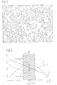
- FIG. 2 illustrates the structure of an internal electrode 2 according to the invention.
- the white circles represent the holes 3.
- the degree of interruption is expressed as a percentage.
- An inner electrode 2 provided with holes can be produced with a suitable thermal process control of the maximum sintering temperature in relation to the liquidus temperature of the inner electrode material.
- the per se known liquidus temperature of the internal electrode material must be above the maximum Sintering temperature of the multilayer piezoelectric actuator are so that the inner electrode just softens when the maximum sintering temperature is reached.
- foils which contain ceramic material with piezoelectric properties, for example lead zirconate titanate.
- ceramic material with piezoelectric properties for example lead zirconate titanate.
- piezoelectrically active ceramic material which has a different composition, for example a mixture of lead zirconate titanate and lead nickel niobate and a material which does not contain lead, for example sodium potassium niobate.
- the films are printed by means of a screen printing process with a paste containing a mixture of silver and palladium in a ratio of preferably between 60 and 95 wt .-% silver and 5 to 40 wt .-% palladium for the preparation of the internal electrodes.
- a ratio of 70 to 30 parts by weight of the respective materials leads to particularly good results.
- an adjustment of the process temperature required for the production of the electrical component is possible in order to form, with different sintering temperatures, the reticular structure of the inner electrode 2, and at the same time to achieve sufficient sintering densification of the ceramic.
- a paste provided for screen printing on the ceramic sheets contains copper or a copper alloy.
- the screen is coated with a film in such a way as to produce a printing pattern in which the Copper layer is provided with circular interruptions or holes each having about 10 to 20 microns in diameter.
- the films printed with the silver palladium paste or with the copper or copper alloy paste are stacked and pressed together to form a stack corresponding to the function of the electrical component.
- the component containing the said mixture also contains silver and palladium as internal electrode is heated to a temperature of 1170 ° and held at this temperature for two hours. This temperature is below the mixing ratio-dependent liquidus temperature of the silver-palladium mixture, which is for a mixing ratio of 70% silver and 30% palladium at 1228 ° C.
- the ceramic is sintered, forming in the inner electrode, the desired network structure.
- the device containing copper or copper alloy as the inner electrode is heated to 1050 ° C after the organic binder is burned out and held at that temperature for two hours while being sintered.
- the reticular structure of the copper electrode is effected by the type of printing with a suitable sieve.
- FIG. 3 shows a SEM image of a net shape formed by the thermal process control inner electrode.
- the expected during sintering number of holes 3 and their accumulated surface can be determined by experience Test results are determined, wherein the formation of the holes of the temperature and the pressure during sintering and the material of the inner electrode is affected.
- FIG. 4 shows qualitatively a curve K, which represents the change in the rigidity of the inner electrode as a function of the degree of interruption UG.
- Curve V shows voltages applied to the multilayer piezoelectric actuator to achieve a given deflection path L of the multilayer piezoelectric actuator.
- the curve L shows different deflection paths, which are achieved with a constant voltage.
- the shape of the curves L and V is also dependent on the degree of interruption of the inner electrode or on its rigidity K. Since the curves V, K, and L all relate to different physical quantities, the left axis of the graph is given without a significant unit. It is particularly preferred that the inner electrode has a degree of interruption within that in the FIG.
- the diameters of the circular holes of the inner electrode are 10 ⁇ m to 15 ⁇ m and / or the areas of non-circular holes are about 50 to 90 ⁇ m 2 .
- These relatively small sizes prevent the holes from forming unwanted and interfering electric fields. With this measure, the electric field over the entire inner electrode considered homogeneous become. For such small holes, it is therefore advantageous to form the holes during sintering according to the manufacturing method according to the invention, since such small holes are difficult to realize by screen printing process.
- the sintered density of the ceramic base body or its dielectric or ceramic layers is related to the geometric structure of the inner electrode. If the internal electrodes are continuous, they provide greater resistance to the tendency of the ceramic body to shrink during sintering. Holes provided internal electrodes in contrast allow the production of multilayer devices with a tendency to higher sintering densities, since the internal electrodes oppose a lower resistance to shrinkage of the ceramic body. Higher sintering densities have the advantage that a greater grain growth accompanied by pore elimination, or reduction of free grain surfaces of the ceramic material is made possible, generally aiming at a reduction of the surface and grain boundary energy, which leads to a decrease in the total free energy of the sintered sintered body.
- the electrical properties of the sintered Krellpiezoaktors are thus improved because, for example, a more homogeneous electromagnetic field distribution and a simpler and predictable deflection behavior of Learntikpiezoaktors is ensured.
- a higher sintering density is therefore of particular interest not only for multilayer piezoactuators but, for example, also for multilayer capacitors.
Landscapes
- Engineering & Computer Science (AREA)
- Manufacturing & Machinery (AREA)
- General Electrical Machinery Utilizing Piezoelectricity, Electrostriction Or Magnetostriction (AREA)
- Fuel-Injection Apparatus (AREA)
- Ceramic Capacitors (AREA)
- Fixed Capacitors And Capacitor Manufacturing Machines (AREA)
Abstract
Description
Die vorliegende Erfindung betrifft ein Vielschichtbauelement sowie ein Verfahren zu dessen Herstellung.The present invention relates to a multilayer component and to a method for its production.
Eine Schlüsselrolle für die Applikation von Vielschichtbauelementen umfassend piezo- und ferroelektrische Aktoren spielt die mechanische Eigensteifigkeit des Bauelements.A key role for the application of multilayer components comprising piezoelectric and ferroelectric actuators is played by the mechanical inherent rigidity of the component.
Aus der
Eine zu lösende Aufgabe besteht darin, ein Vielschichtbauelement anzugeben, welches bei möglichst geringer Spannung einen hohen Auslenkungsweg erreicht.An object to be solved is to specify a multilayer component which achieves a high deflection path with the lowest possible voltage.
Die Aufgabe wird hinsichtlich eines Vielschichtbauelements und hinsichtlich der Herstellung eines Vielschichtbauelements durch die Merkmale der jeweiligen unabhängigen Ansprüche gelöst.The object is achieved with regard to a multilayer component and with regard to the production of a multilayer component by the features of the respective independent claims.
Es wird ein Vielschichtbauelement vorgeschlagen, welches folgende Merkmale umfasst: einen keramischen Grundkörper und mindestens eine im keramischen Grundkörper angeordnete Innenelektrode, wobei die Innenelektrode mehrere Löcher aufweist.A multilayer component is proposed, which comprises the following features: a ceramic base body and at least one inner electrode arranged in the ceramic base body, the inner electrode having a plurality of holes.
Ein solches Vielschichtbauelement hat den Vorteil, dass die Steifigkeit der Innenelektrode entgegen einer queraxialen Kontraktion teilweise oder ganz verringert wird und dadurch während einer axialen Auslenkung des Vielschichtbauelements eine quasi störungsfreie queraxiale Querkontraktion der Innenelektrode möglich ist. Mit der Querkontraktion wird gleichzeitig bei gleicher angelegter Spannung ein höherer axialer Auslenkungsweg des Vielschichtbauelements erreicht.Such a multilayer component has the advantage that the rigidity of the inner electrode against a transverse axial contraction is partially or completely reduced and thereby a quasi interference-free transverse axial transverse contraction of the inner electrode is possible during an axial deflection of the multilayer component. With the transverse contraction, a higher axial deflection path of the multilayer component is simultaneously achieved with the same applied voltage.
Das Vielschichtbauelement kann vorteilhafterweise dichter gesintert werden, da eine mit mehreren Löchern versehene Innenelektrode einen geringeren mechanischen Widerstand gegenüber der Keramik des Grundkörpers stellt, welche während des Sinterns stets zu schrumpfen bestrebt ist. Eine höhere Sinterdichte wird von verbesserten elektrischen Eigenschaften begleitet, und ist somit von Vorteil. Eine höhere Sinterdichte ermöglicht außerdem auch einen höheren Auslenkungsweg. Bei einem Piezoktor kann dies je nach Anwendung von besonderem Vorteil sein.The multilayer component can advantageously be densely sintered, since an inner electrode provided with a plurality of holes provides a lower mechanical resistance to the ceramic of the base body, which always strives to shrink during sintering. A higher sintering density is accompanied by improved electrical properties, and is thus advantageous. A higher sintering density also allows a higher deflection path. Depending on the application, this can be of particular advantage for a piezoelectric actuator.
Zur Herstellung eines Vielschichtbauelements wird vorgeschlagen, dass keramische Folien bereitgestellt werden, auf die Innenelektrodenmaterial, vorzugsweise in der Form einer Paste, gedruckt wird. Die Folien werden gestapelt, geschnitten oder erst geschnitten und dann gestapelt. Das so erhaltene Vielschichtbauelement wird anschließend gesintert.To produce a multilayer component, it is proposed that ceramic films be provided on which inner electrode material, preferably in the form of a paste, is printed. The films are stacked, cut or first cut and then stacked. The multilayer component thus obtained is then sintered.
Es wird bevorzugt, als Innenelektrodenmaterial eine Silber-Palladium Mischung zu verwenden, wobei vorzugsweise Silber in einem Gewichtsanteil von zwischen 60 und 80% und Palladium in einem Gewichtsanteil von zwischen 20 und 40% vorhanden ist.It is preferred to use as internal electrode material a silver-palladium mixture, wherein preferably silver is present in a weight fraction of between 60 and 80% and palladium in a weight fraction of between 20 and 40%.
Aus dieser Mischung wird eine Paste gebildet, welche auf die zu stapelnde keramische Folien gedruckt wird. Das so erhaltene Bauelement wird bei einer Temperatur zwischen 1120 und 1220°C, vorzugsweise bei 1170°C, gesintert, wobei das Innenelektrodenmaterial während des Sintervorgangs gerade ausreichend erweicht, dass sich eine netzförmige Struktur bildet.From this mixture, a paste is formed, which is printed on the ceramic films to be stacked. That so The component obtained is sintered at a temperature between 1120 and 1220 ° C, preferably at 1170 ° C, wherein the internal electrode material softens just enough during the sintering process to form a reticular structure.
Es wird insbesondere bevorzugt, dass ein Innenelektrodenmaterial verwendet wird, dessen Liquidustemperatur sich derart geringfügig von der Sintertemperatur des keramischen Grundkörpers unterscheidet, dass der keramische Grundkörper gesintert wird und gleichzeitig die Innenelektrode mehrere Löcher bildet. Es ergibt sich der Vorteil, dass kleine Löcher in der Innenelektrodenschicht erzeugt werden können. Dabei fällt die elektromagnetische Feldverteilung der Innenelektrode homogener aus, je kleiner die Löcher der Innenelektrode ausgebildet werden.It is particularly preferred that an internal electrode material is used whose liquidus temperature is so slightly different from the sintering temperature of the ceramic base body that the ceramic base body is sintered and at the same time the internal electrode forms a plurality of holes. This results in the advantage that small holes can be produced in the inner electrode layer. In this case, the electromagnetic field distribution of the inner electrode is more homogeneous, the smaller the holes of the inner electrode are formed.
Alternativ kann als Innenelektrodenmaterial Kupfer oder eine Kupferlegierung verwendet werden. Das Material wird in der Form einer Paste mittels Siebdrucken auf die keramische Folien gebracht, wobei ein Sieb verwendet wird, das vorzugsweise zu einem Bedruckungsmuster der Innenelektrode führt, das Löcher bzw. Unterbrechungen mit Durchmessern zwischen 10 und 20 µm aufweist. Nach dem Stapeln der Folien wird das dadurch erhaltene Bauelement bei einer Temperatur zwischen 1000°C und 1100°C, vorzugsweise bei 1050°C, gesintert.Alternatively, as the internal electrode material, copper or a copper alloy may be used. The material is screen-printed onto the ceramic sheets in the form of a paste, using a screen which preferably results in a printed pattern of the inner electrode having holes with diameters between 10 and 20 μm. After stacking the films, the resulting device is sintered at a temperature between 1000 ° C and 1100 ° C, preferably at 1050 ° C, sintered.
Im Folgenden wird ein Vielschichtbauelement anhand bevorzugter Ausführungsbeispiele näher erläutert. Dabei zeigt
- Figur 1
- einen Vielschichtpiezoaktor mit einer Piezokeramikschicht welche an eine mit Löchern versehenen Innenelektrode angrenzt,
Figur 2- eine vergrößerte Darstellung der mit Löchern versehenen Elektrode,
Figur 3- eine zweidimensionale fotographische Abbildung einer mit Löchern versehenen Innenelektrode,
- Figur 4
- eine Graphik zur Darstellung einer bevorzugten, optimalen Einstellung eines durch die Löcher erzeugten Unterbrechungsgrades der Innenelektrode, einer auf den Vielschichtpiezoaktor anzulegenden Spannung und eines Auslenkungswegs des Vielschichtpiezoaktors.
- FIG. 1
- a multilayer piezoelectric actuator having a piezoceramic layer adjacent to a perforated inner electrode,
- FIG. 2
- an enlarged view of the perforated electrode,
- FIG. 3
- a two-dimensional photographic image of a perforated inner electrode,
- FIG. 4
- a graph showing a preferred, optimal setting of a generated by the holes degree of interruption of the inner electrode, to be applied to the Vielschichtpiezoaktor voltage and a deflection path of the Vielschichtpiezoaktors.
Es wird ein Weg aufgezeigt, wie bei gegebener Bauteilgeometrie und vorgegebenem Keramik- und Innenelektrodenmaterial die Steifigkeit des Vielschichtbauelements aktiv variiert werden kann.A way is shown how, given the geometry of the component and the given ceramic and inner electrode material, the rigidity of the multilayer component can be actively varied.
Es wurde für Testzwecke, beispielsweise auf einem Kraft- oder Auslenkungsmeßplatz, die Steifigkeit von Vielschichtaktoren gemessen. Der sich aus der Messung ergebende integrale Bauteilsteifigkeitswert wurde dabei eins zu eins der Elastizität der Keramik zugeschrieben. In anderen Worten: ein höherer Steifigkeitswert indizierte eine härtere Keramik, je nachdem, ob die Keramik donatordotiert oder akzeptordotiert wurde. Aus dieser Überlegung heraus wurde vor allem über die Zusammensetzung der Keramik (Keramikrezeptur) versucht, den E-Modul des Vielschichtpiezoaktors und somit die Bauteilsteifigkeit einzustellen.The stiffness of multilayer actuators was measured for testing purposes, for example on a force or displacement measuring station. The integral component stiffness value resulting from the measurement was attributed one to one to the elasticity of the ceramic. In other words, a higher stiffness index indicated a harder ceramic, depending on whether the ceramic was donor-doped or acceptor doped. Based on this consideration, it was above all the composition of the ceramic (ceramic formulation) that sought to set the modulus of elasticity of the multilayer piezoactuator and thus the component rigidity.
Allgemein kann aber die Steifigkeit K eines Vielschichtbauelements in einem ersten Schritt über die Formel 
Im Folgenden wird angenommen, dass das Vielschichtbauelement einen Vielschichtpiezoaktor umfasst, wobei andere Vielschichtbauelemente ebenfalls möglich sind, wie beispielsweise Vielschichtkondensatoren oder andere Keramikumfassende Vielschichtbauelemente.In the following, it is assumed that the multilayer component comprises a multilayer piezoactuator, wherein other multilayer components are also possible, such as multilayer capacitors or other multilayer ceramic devices.
Die Eigensteifigkeit des in
Es ist eine Eigenschaft piezo/ferroelektrischer Materialien, sich bei anliegender elektrischer Spannung auszulenken. Mit der Auslenkung in eine Raumrichtung, beispielsweise die axiale Richtung (unterer Pfeil), geht eine queraxiale Kontraktion (oberer Pfeil) oder Querkontraktion in den Raumrichtungen normal auf die Auslenkungsrichtung einher. Bei Vielschichtpiezoaktoren mit durchgehenden Innenelektroden stehen dieser Querkontraktion die Innenelektroden als mechanischer Gegenspieler entgegen und reduzieren dadurch im Vergleich zu einem monolithischen Keramikquader ohne Innenelektroden die Querkontraktion und damit auch die Auslenkung des Bauteils.It is a characteristic of piezo / ferroelectric materials to deflect when voltage is applied. With the deflection in a spatial direction, for example the axial direction (lower arrow), a transverse axial contraction (upper arrow) or transverse contraction in the spatial directions is normal to the deflection direction. In multilayer piezoelectric actuators with continuous internal electrodes, this transverse contraction opposes the internal electrodes as mechanical counterparts and thereby reduces the transverse contraction and thus also the deflection of the component in comparison to a monolithic ceramic cuboid without internal electrodes.
Um also die Querkontraktion zu erleichtern werden erfindungsgemäß die Innenelektroden 2 mit Löchern versehen, wobei es aber nicht erforderlich ist, dass die Löcher die Innenelektrode ganz durchbohren- vorzugsweise können sie auch als erhebliche Einbuchtungen realisiert sein.Thus, to facilitate the transverse contraction, according to the invention, the
Über die beiden Parameter Dicke d der Innenelektroden 2 und des Unterbrechungsgrades 3D, das heißt die Anzahl der Löcher 3 in der Innenelektrode pro Flächeneinheit der Innenelektrode, lassen sich der integrale E-Modul des Vielschichtpiezoaktors und somit seine Steifigkeit bei einer gegebenen Geometrie variieren. Im Profilschliff zeigt sich der Unterbrechungsgrad 3D als elektrodenmaterialfreie Bereiche innerhalb der Innenelektrode. Zur Anpassung der Bauteilsteifigkeit sind also zwei Parameter vorgesehen: die Dicke d der Innenelektrode 2 und der Unterbrechungsgrad 3D der Innenelektrode.By way of the two parameters thickness d of the
Dabei wird bevorzugt, dass die Dicke der Innenelektroden so gering wie möglich gehalten wird, da hiermit einerseits geringere Mengen an Elektrodenmaterial verwendet werden müssen und somit geringere Kosten anfallen, und andererseits eine höhere Sinterdichte des Vielschichtbauelements erreicht werden kann. Der Vielschichtpiezoaktor ist vorzugsweise so ausgebildet, dass die Innenelektroden mit einer elektrisch leitenden Kontaktschicht verbunden sind um die elektrische Verbindung an eine Spannungs- und Stromquelle herzustellen.It is preferred that the thickness of the internal electrodes is kept as low as possible, since on the one hand smaller amounts of electrode material are used and thus lower costs incurred, and on the other hand, a higher sintering density of the multilayer component can be achieved. The multilayer piezoelectric actuator is preferably designed such that the internal electrodes are connected to an electrically conductive contact layer in order to produce the electrical connection to a voltage and current source.

Eine mit Löchern versehene Innenelektrode 2 kann mit einer geeigneten thermischen Prozessführung der maximalen Sintertemperatur in Relation zur Liquidustemperatur des Innenelektrodenmaterials hergestellt werden. Je kleiner die Temperaturdifferenz zwischen der Liquidustemperatur des Innenelektrodenmaterials und der maximalen Sintertemperatur des Vielschichtpiezoaktors eingestellt wird, desto mehr zieht sich die Innenelektrode zusammen, so dass eine durchlöcherte Struktur der Innenelektrode gemäß der
Zur Herstellung eines elektrischen Bauelements mit einer mit Löchern versehenen Innenelektrode 2 werden Folien bereitgestellt, die keramisches Material mit piezoelektrischen Eigenschaften, beispielsweise Bleizirkonat-Titanat, enthalten. Es ist jedoch auch piezoelektrisch aktives keramisches Material einsetzbar, das eine andere Zusammensetzung aufweist, wie zum Beispiel eine Mischung aus Bleizirkonat-Titanat und Blei-Nickelniobat sowie ein Material, das kein Blei enthält, wie zum Beispiel Natrium-Kaliumniobat.To produce an electrical component with a perforated
Die Folien werden zur Herstellung der Innenelektroden mittels eines Siebdruckverfahrens mit einer Paste bedruckt, die ein Gemisch aus Silber und Palladium in einem Verhältnis von vorzugsweise zwischen 60 und 95 Gew.-% Silber und 5 bis 40 Gew.-% Palladium enthält. Insbesondere führt ein Verhältnis von 70 zu 30 Gewichtsanteilen der jeweiligen Materialien zu besonders guten Ergebnissen. Anhand einer Änderung dieser Gewichtsanteile ist eine Anpassung der für die Herstellung des elektrischen Bauelements erforderlichen Prozesstemperatur möglich, um bei unterschiedlichen keramischen Materialien mit unterschiedlichen Sintertemperaturen die netzförmige Struktur der Innenelektrode 2 zu formen, einzustellen und gleichzeitig eine ausreichende Sinterverdichtung der Keramik zu erreichen.The films are printed by means of a screen printing process with a paste containing a mixture of silver and palladium in a ratio of preferably between 60 and 95 wt .-% silver and 5 to 40 wt .-% palladium for the preparation of the internal electrodes. In particular, a ratio of 70 to 30 parts by weight of the respective materials leads to particularly good results. On the basis of a change in these weight proportions, an adjustment of the process temperature required for the production of the electrical component is possible in order to form, with different sintering temperatures, the reticular structure of the
Gemäß einer Ausführungsform enthält eine zum Siebdrucken auf die Keramikfolien bereitgestellte Paste Kupfer oder eine Kupferlegierung. Das Sieb ist derart mit einem Film beschichtet, dass ein Bedruckungsmuster entsteht, bei dem die Kupferschicht mit kreisförmigen Unterbrechungen bzw. Löchern mit jeweils etwa 10 bis 20 µm Durchmesser versehen wird.In one embodiment, a paste provided for screen printing on the ceramic sheets contains copper or a copper alloy. The screen is coated with a film in such a way as to produce a printing pattern in which the Copper layer is provided with circular interruptions or holes each having about 10 to 20 microns in diameter.
Die mit der Silber-Palladiumpaste oder mit der Kupfer- oder der Kupferlegierungspaste bedruckten Folien werden in der Weise gestapelt und miteinander verpresst, dass ein der Funktion des elektrischen Bauelements entsprechender Stapel entsteht.The films printed with the silver palladium paste or with the copper or copper alloy paste are stacked and pressed together to form a stack corresponding to the function of the electrical component.
Nach dem Ausbrand des in der Folie und in der Metallpaste enthaltenen organischen Bindemittels wird das Bauelement, das die genannten Mischung auch Silber und Palladium als Innenelektrode enthält, auf eine Temperatur von 1170° erwärmt und bei dieser Temperatur zwei Stunden lang gehalten. Diese Temperatur liegt unter der mischungsverhältnisabhängigen Liquidustemperatur der Silber-Palladium Mischung, die für ein Mischungsverhältnis von 70 % Silber und 30 % Palladium bei 1228°C liegt. Dabei wird die Keramik gesintert, wobei sich in der Innenelektrode sich die erwünschte Netzstruktur ausbildet.After the burnout of the organic binder contained in the film and in the metal paste, the component containing the said mixture also contains silver and palladium as internal electrode is heated to a temperature of 1170 ° and held at this temperature for two hours. This temperature is below the mixing ratio-dependent liquidus temperature of the silver-palladium mixture, which is for a mixing ratio of 70% silver and 30% palladium at 1228 ° C. The ceramic is sintered, forming in the inner electrode, the desired network structure.
Das Bauelement, das Kupfer oder die Kupferlegierung als Innenelektrode enthält, wird nach dem Ausbrand des organischen Bindemittels auf 1050°C erwärmt und bei dieser Temperatur zwei Stunden lang gehalten und währenddessen gesintert. Die netzförmige Struktur der Kupferelektrode erfolgt durch die Art der Bedruckung mit einem geeigneten Sieb.The device containing copper or copper alloy as the inner electrode is heated to 1050 ° C after the organic binder is burned out and held at that temperature for two hours while being sintered. The reticular structure of the copper electrode is effected by the type of printing with a suitable sieve.
Die beim Sintern zu erwartende Anzahl der Löcher 3 und deren aufsummierte Fläche kann durch Erfahrungswerte aus Testergebnissen ermittelt werden, wobei die Bildung der Löcher von der Temperatur und dem Druck beim Sintern sowie vom Material der Innenelektrode beeinflusst wird.The expected during sintering number of
Es wird bevorzugt, dass die Durchmesser der kreisförmigen Löcher der Innenelektrode bei 10µm bis 15µm liegen und/oder die Flächen von nichtkreisförmigen Löchern bei ca. 50 bis 90 µm2 liegen. Diese relativ geringen Größen verhindern, dass sich an den Löchern unerwünschte und störende elektrische Felder bilden. Mit dieser Maßnahme kann das elektrische Feld über der gesamten Innenelektrode als homogen betrachtet werden. Für derart kleine Löcher ist es daher vorteilhaft, die Löcher während des Sinterns nach dem erfindungsgemäßen Herstellungsverfahrens auszubilden, da per Siebdruckverfahren derart kleine Löcher schwer zu realisieren sind.It is preferable that the diameters of the circular holes of the inner electrode are 10 μm to 15 μm and / or the areas of non-circular holes are about 50 to 90 μm 2 . These relatively small sizes prevent the holes from forming unwanted and interfering electric fields. With this measure, the electric field over the entire inner electrode considered homogeneous become. For such small holes, it is therefore advantageous to form the holes during sintering according to the manufacturing method according to the invention, since such small holes are difficult to realize by screen printing process.
Die Sinterdichte des keramischen Grundkörpers, bzw. dessen Dielektrikums- oder Keramikschichten hängt mit der geometrischen Struktur der Innenelektrode zusammen. Sind die Innenelektroden durchgängig, stellen diese einen größeren Widerstand gegenüber dem Bestreben des keramischen Grundkörpers während des Sinterns zu schrumpfen entgegen. Mit Löchern versehene Innenelektroden erlauben in Gegensatz dazu die Herstellung von Vielschichtbauelementen mit tendenziell höheren Sinterdichten, da die Innenelektroden einen geringeren Widerstand gegenüber dem Schrumpfen des keramischen Grundkörpers entgegenstellen. Höhere Sinterdichten haben den Vorteil, dass ein größeres Kornwachstum begleitet von Poreneliminierung, bzw. Reduzierung freier Kornoberflächen des keramischen Materials ermöglicht wird, wobei im Allgemeinen eine Verringerung der Oberflächen- und Korngrenzenenergie angestrebt wird, die zu einer Erniedrigung der gesamten freien Enthalpie des Sinterkörpers führt. Die elektrischen Eigenschaften des gesinterten Vielschichtpiezoaktors werden somit verbessert, da beispielsweise eine homogenere elektromagnetische Feldverteilung und ein einfacheres und voraussehbares Auslenkungsverhalten des Vielschichtpiezoaktors gewährleistet wird. Eine höhere Sinterdichte ist daher auch nicht nur für Vielschichtpiezoaktoren, sondern beispielsweise auch für Vielschichtkondensatoren, von besonderem Interesse.The sintered density of the ceramic base body or its dielectric or ceramic layers is related to the geometric structure of the inner electrode. If the internal electrodes are continuous, they provide greater resistance to the tendency of the ceramic body to shrink during sintering. Holes provided internal electrodes in contrast allow the production of multilayer devices with a tendency to higher sintering densities, since the internal electrodes oppose a lower resistance to shrinkage of the ceramic body. Higher sintering densities have the advantage that a greater grain growth accompanied by pore elimination, or reduction of free grain surfaces of the ceramic material is made possible, generally aiming at a reduction of the surface and grain boundary energy, which leads to a decrease in the total free energy of the sintered sintered body. The electrical properties of the sintered Vielschichtpiezoaktors are thus improved because, for example, a more homogeneous electromagnetic field distribution and a simpler and predictable deflection behavior of Vielschichtpiezoaktors is ensured. A higher sintering density is therefore of particular interest not only for multilayer piezoactuators but, for example, also for multilayer capacitors.
- 11
- keramische Schichtceramic layer
- 22
- Innenelektrodeinner electrode
- 33
- Loch einer InnenelektrodeHole of an inner electrode
- AA
- Querschnittsfläche eines PiezoaktorsCross-sectional area of a piezoelectric actuator
- ll
- Länge des PiezoaktorsLength of the piezo actuator
- bb
- Länge einer Seite einer InnenelektrodeLength of one side of an inner electrode
- PP
- Piezoaktorpiezo actuator
Claims (12)
Applications Claiming Priority (2)
| Application Number | Priority Date | Filing Date | Title |
|---|---|---|---|
| DE102004038103A DE102004038103A1 (en) | 2004-08-05 | 2004-08-05 | Multi-layer component and method for its production |
| EP05774389A EP1774603B1 (en) | 2004-08-05 | 2005-08-05 | Multi-layered component and method for the production thereof |
Related Parent Applications (2)
| Application Number | Title | Priority Date | Filing Date |
|---|---|---|---|
| EP05774389A Division EP1774603B1 (en) | 2004-08-05 | 2005-08-05 | Multi-layered component and method for the production thereof |
| EP05774389.0 Division | 2005-08-05 |
Publications (3)
| Publication Number | Publication Date |
|---|---|
| EP2256836A2 true EP2256836A2 (en) | 2010-12-01 |
| EP2256836A3 EP2256836A3 (en) | 2011-01-05 |
| EP2256836B1 EP2256836B1 (en) | 2012-10-10 |
Family
ID=35044666
Family Applications (2)
| Application Number | Title | Priority Date | Filing Date |
|---|---|---|---|
| EP05774389A Ceased EP1774603B1 (en) | 2004-08-05 | 2005-08-05 | Multi-layered component and method for the production thereof |
| EP10179362A Ceased EP2256836B1 (en) | 2004-08-05 | 2005-08-05 | Method for fabrication of a multilayer element |
Family Applications Before (1)
| Application Number | Title | Priority Date | Filing Date |
|---|---|---|---|
| EP05774389A Ceased EP1774603B1 (en) | 2004-08-05 | 2005-08-05 | Multi-layered component and method for the production thereof |
Country Status (5)
| Country | Link |
|---|---|
| US (1) | US7692368B2 (en) |
| EP (2) | EP1774603B1 (en) |
| JP (1) | JP5069112B2 (en) |
| DE (1) | DE102004038103A1 (en) |
| WO (1) | WO2006012891A1 (en) |
Cited By (1)
| Publication number | Priority date | Publication date | Assignee | Title |
|---|---|---|---|---|
| DE102011113496A1 (en) * | 2011-09-15 | 2013-03-21 | Epcos Ag | Multi-layer component and method for its production |
Families Citing this family (9)
| Publication number | Priority date | Publication date | Assignee | Title |
|---|---|---|---|---|
| DE102004020329A1 (en) * | 2004-04-26 | 2005-11-10 | Epcos Ag | Electrical functional unit and method for its production |
| DE102005017108A1 (en) * | 2005-01-26 | 2006-07-27 | Epcos Ag | Piezoelectric multi-layer component e.g. piezo-ceramic piezo actuator, has base with dielectric thicknesses and inner electrodes, and contact units of porous material running perpendicularly to electrodes |
| JP5256804B2 (en) * | 2008-03-19 | 2013-08-07 | Tdk株式会社 | Piezoelectric ceramic and piezoelectric element using the same |
| DE102008029426A1 (en) | 2008-06-23 | 2010-01-07 | Epcos Ag | Method for producing a multilayer component, multilayer component and template |
| CN102473836A (en) * | 2009-08-27 | 2012-05-23 | 京瓷株式会社 | Multilayer piezoelectric element, and injection apparatus and fuel injection system using same |
| EP2709526B1 (en) | 2011-05-17 | 2021-06-30 | University Health Network | Breathing disorder identification methods and systems |
| EP2840621B1 (en) * | 2012-04-19 | 2019-01-02 | NGK Insulators, Ltd. | Film-type piezoelectric/electrostrictive element |
| JP2014072329A (en) * | 2012-09-28 | 2014-04-21 | Taiheiyo Cement Corp | Method of manufacturing piezoelectric element |
| CA2931662C (en) | 2015-11-03 | 2023-09-26 | University Health Network | Acoustic upper airway assessment system and method, and sleep apnea assessment system and method relying thereon |
Citations (1)
| Publication number | Priority date | Publication date | Assignee | Title |
|---|---|---|---|---|
| WO1999012865A1 (en) | 1997-09-05 | 1999-03-18 | Ceramtec Ag Innovative Ceramic Engineering | High-performance piezoelectric ceramic |
Family Cites Families (16)
| Publication number | Priority date | Publication date | Assignee | Title |
|---|---|---|---|---|
| EP0094078B1 (en) * | 1982-05-11 | 1988-11-02 | Nec Corporation | Multilayer electrostrictive element which withstands repeated application of pulses |
| US4803763A (en) * | 1986-08-28 | 1989-02-14 | Nippon Soken, Inc. | Method of making a laminated piezoelectric transducer |
| JPS63142875A (en) | 1986-12-05 | 1988-06-15 | Sumitomo Special Metals Co Ltd | Piezoelectric laminated actuator |
| JP2567046B2 (en) * | 1987-09-25 | 1996-12-25 | 日立金属株式会社 | Stacked displacement element |
| JPH0352211A (en) * | 1989-07-20 | 1991-03-06 | Matsushita Electric Ind Co Ltd | Laminated ceramic capacitor |
| JP2893741B2 (en) * | 1989-08-02 | 1999-05-24 | 日本電気株式会社 | Electrostrictive effect element |
| JP3043387B2 (en) * | 1990-10-01 | 2000-05-22 | 日立金属株式会社 | Stacked displacement element |
| JPH0855753A (en) * | 1994-08-10 | 1996-02-27 | Taiyo Yuden Co Ltd | Layered ceramic capacitor and manufacture thereof |
| DE19946836A1 (en) * | 1999-09-30 | 2000-11-09 | Bosch Gmbh Robert | Piezoactuator for operating a mechanical component, such as a valves in vehicle fuel injection systems has a multilayer structure of piezolayers with inner electrodes arranged between them |
| DE10006352A1 (en) * | 2000-02-12 | 2001-08-30 | Bosch Gmbh Robert | Piezoelectric ceramic body with silver-containing internal electrodes |
| JP2002075774A (en) | 2000-09-04 | 2002-03-15 | Furuya Kinzoku:Kk | Electronic component |
| JP2002198250A (en) * | 2000-12-26 | 2002-07-12 | Kyocera Corp | Laminated electronic component |
| JP2002208533A (en) | 2001-01-09 | 2002-07-26 | Matsushita Electric Ind Co Ltd | Laminated ceramic electronic component and its manufacturing method |
| US7304414B2 (en) * | 2002-05-06 | 2007-12-04 | Epcos Ag | Piezoactuator and method for the production thereof |
| EP2037511A3 (en) * | 2003-09-24 | 2009-04-22 | Kyocera Corporation | Multilayer piezoelectric element |
| CN101694865B (en) * | 2004-03-09 | 2013-03-20 | 京瓷株式会社 | Multilayer piezoelectric element and its manufacturing method |
-
2004
- 2004-08-05 DE DE102004038103A patent/DE102004038103A1/en not_active Ceased
-
2005
- 2005-08-05 US US11/573,229 patent/US7692368B2/en not_active Expired - Fee Related
- 2005-08-05 WO PCT/DE2005/001389 patent/WO2006012891A1/en active Application Filing
- 2005-08-05 EP EP05774389A patent/EP1774603B1/en not_active Ceased
- 2005-08-05 EP EP10179362A patent/EP2256836B1/en not_active Ceased
- 2005-08-05 JP JP2007524175A patent/JP5069112B2/en not_active Expired - Fee Related
Patent Citations (1)
| Publication number | Priority date | Publication date | Assignee | Title |
|---|---|---|---|---|
| WO1999012865A1 (en) | 1997-09-05 | 1999-03-18 | Ceramtec Ag Innovative Ceramic Engineering | High-performance piezoelectric ceramic |
Cited By (2)
| Publication number | Priority date | Publication date | Assignee | Title |
|---|---|---|---|---|
| DE102011113496A1 (en) * | 2011-09-15 | 2013-03-21 | Epcos Ag | Multi-layer component and method for its production |
| US9583262B2 (en) | 2011-09-15 | 2017-02-28 | Epcos Ag | Multi-layer component and method for producing same |
Also Published As
| Publication number | Publication date |
|---|---|
| EP2256836B1 (en) | 2012-10-10 |
| US20080030105A1 (en) | 2008-02-07 |
| EP1774603A1 (en) | 2007-04-18 |
| WO2006012891A1 (en) | 2006-02-09 |
| US7692368B2 (en) | 2010-04-06 |
| JP2008508737A (en) | 2008-03-21 |
| JP5069112B2 (en) | 2012-11-07 |
| EP1774603B1 (en) | 2013-03-20 |
| EP2256836A3 (en) | 2011-01-05 |
| DE102004038103A1 (en) | 2006-02-23 |
Similar Documents
| Publication | Publication Date | Title |
|---|---|---|
| EP1774603B1 (en) | Multi-layered component and method for the production thereof | |
| EP1597780B1 (en) | Electrical multilayered component and layer stack | |
| DE10208417A1 (en) | Laminated piezoelectric device used, e.g. for fuel injection devices in vehicles comprises a rod-like laminate formed by alternately laminating piezoelectric layers and electrode layers | |
| EP2436051B1 (en) | Piezoelectric component | |
| EP1863104B1 (en) | Method of manufacturing a multi-layered ceramic component | |
| DE19814697C1 (en) | Piezoelectric actuator, especially multilayer ceramic piezo-actuator used as positioning device, ultrasonic emitter, valve controller or sensor | |
| EP2577762B1 (en) | Method for producing a piezo actuator and piezo actuator | |
| EP2529423B1 (en) | Piezo electrical component | |
| EP1129493B1 (en) | Piezoceramic multi-layer structure with regular polygon cross-sectional area | |
| DE102020126404B4 (en) | Piezoelectric multilayer component | |
| EP1497838A1 (en) | Positive temperature coefficient (ptc) component and method for the production thereof | |
| EP2847805B1 (en) | Method for producing a multi-layered structural element, and a multi-layered structural element produced according to said method | |
| EP2798679B1 (en) | Piezo-stack with passivation, and a method for the passivation of a piezo-stack | |
| WO2015022154A1 (en) | Multilayer component comprising an external contact and method for producing a multilayer component comprising an external contact | |
| DE102004005528A1 (en) | Laminated piezoelectric element used as a drive source for injecting into a vehicle, comprises a laminated body containing piezoelectric layers, and a pair of lateral electrode layers made from a porous material | |
| DE102020118857B4 (en) | Multilayer capacitor | |
| DE102007000730B4 (en) | Stacked piezoceramic element, use and manufacturing process | |
| DE102017108384A1 (en) | Multi-layer component and method for producing a multilayer component | |
| DE102020107305B4 (en) | Piezoelectric multilayer element | |
| DE112017000681T5 (en) | Ozone generating device and ozone generating device | |
| DD293689A5 (en) | LAMINATED CERAMIC ARRANGEMENT AND METHOD OF MANUFACTURING THE SAME | |
| DE10121271A1 (en) | Green body, piezoelectric component and method for producing a piezoelectric component | |
| DE102019206018A1 (en) | Electromechanical actuator with ceramic insulation, method for its production and method for controlling such an actuator | |
| WO2011101473A1 (en) | Piezoelectric multilayer component and method for producing a piezoelectric multilayer component |
Legal Events
| Date | Code | Title | Description |
|---|---|---|---|
| PUAI | Public reference made under article 153(3) epc to a published international application that has entered the european phase |
Free format text: ORIGINAL CODE: 0009012 |
|
| AC | Divisional application: reference to earlier application |
Ref document number: 1774603 Country of ref document: EP Kind code of ref document: P |
|
| AK | Designated contracting states |
Kind code of ref document: A2 Designated state(s): DE |
|
| PUAL | Search report despatched |
Free format text: ORIGINAL CODE: 0009013 |
|
| AK | Designated contracting states |
Kind code of ref document: A3 Designated state(s): DE |
|
| 17P | Request for examination filed |
Effective date: 20110705 |
|
| RTI1 | Title (correction) |
Free format text: METHOD FOR FABRICATION OF A MULTILAYER ELEMENT |
|
| GRAP | Despatch of communication of intention to grant a patent |
Free format text: ORIGINAL CODE: EPIDOSNIGR1 |
|
| GRAS | Grant fee paid |
Free format text: ORIGINAL CODE: EPIDOSNIGR3 |
|
| GRAA | (expected) grant |
Free format text: ORIGINAL CODE: 0009210 |
|
| AC | Divisional application: reference to earlier application |
Ref document number: 1774603 Country of ref document: EP Kind code of ref document: P |
|
| AK | Designated contracting states |
Kind code of ref document: B1 Designated state(s): DE |
|
| REG | Reference to a national code |
Ref country code: DE Ref legal event code: R096 Ref document number: 502005013184 Country of ref document: DE Effective date: 20121220 |
|
| PLBE | No opposition filed within time limit |
Free format text: ORIGINAL CODE: 0009261 |
|
| STAA | Information on the status of an ep patent application or granted ep patent |
Free format text: STATUS: NO OPPOSITION FILED WITHIN TIME LIMIT |
|
| 26N | No opposition filed |
Effective date: 20130711 |
|
| REG | Reference to a national code |
Ref country code: DE Ref legal event code: R097 Ref document number: 502005013184 Country of ref document: DE Effective date: 20130711 |
|
| PGFP | Annual fee paid to national office [announced via postgrant information from national office to epo] |
Ref country code: DE Payment date: 20180823 Year of fee payment: 14 |
|
| REG | Reference to a national code |
Ref country code: DE Ref legal event code: R082 Ref document number: 502005013184 Country of ref document: DE Representative=s name: EPPING HERMANN FISCHER PATENTANWALTSGESELLSCHA, DE Ref country code: DE Ref legal event code: R081 Ref document number: 502005013184 Country of ref document: DE Owner name: TDK ELECTRONICS AG, DE Free format text: FORMER OWNER: EPCOS AG, 81669 MUENCHEN, DE |
|
| REG | Reference to a national code |
Ref country code: DE Ref legal event code: R119 Ref document number: 502005013184 Country of ref document: DE |
|
| PG25 | Lapsed in a contracting state [announced via postgrant information from national office to epo] |
Ref country code: DE Free format text: LAPSE BECAUSE OF NON-PAYMENT OF DUE FEES Effective date: 20200303 |