EP2255389B1 - Stacked image sensor with shared diffusion regions - Google Patents
Stacked image sensor with shared diffusion regions Download PDFInfo
- Publication number
- EP2255389B1 EP2255389B1 EP09721716.0A EP09721716A EP2255389B1 EP 2255389 B1 EP2255389 B1 EP 2255389B1 EP 09721716 A EP09721716 A EP 09721716A EP 2255389 B1 EP2255389 B1 EP 2255389B1
- Authority
- EP
- European Patent Office
- Prior art keywords
- positions
- array
- image sensor
- photosensitive elements
- wafer
- Prior art date
- Legal status (The legal status is an assumption and is not a legal conclusion. Google has not performed a legal analysis and makes no representation as to the accuracy of the status listed.)
- Active
Links
- 238000009792 diffusion process Methods 0.000 title claims description 76
- 238000012545 processing Methods 0.000 claims description 17
- 238000000034 method Methods 0.000 claims description 9
- 235000012431 wafers Nutrition 0.000 description 58
- 239000002184 metal Substances 0.000 description 13
- 238000006243 chemical reaction Methods 0.000 description 10
- 239000004020 conductor Substances 0.000 description 9
- 238000003384 imaging method Methods 0.000 description 8
- 238000001465 metallisation Methods 0.000 description 8
- 239000004065 semiconductor Substances 0.000 description 7
- 238000012546 transfer Methods 0.000 description 7
- 238000003491 array Methods 0.000 description 6
- 229910052710 silicon Inorganic materials 0.000 description 6
- 239000010703 silicon Substances 0.000 description 6
- XUIMIQQOPSSXEZ-UHFFFAOYSA-N Silicon Chemical compound [Si] XUIMIQQOPSSXEZ-UHFFFAOYSA-N 0.000 description 5
- 239000000969 carrier Substances 0.000 description 5
- 239000000463 material Substances 0.000 description 5
- 230000035945 sensitivity Effects 0.000 description 5
- 238000010586 diagram Methods 0.000 description 4
- 239000000758 substrate Substances 0.000 description 4
- 206010034960 Photophobia Diseases 0.000 description 3
- 238000002955 isolation Methods 0.000 description 3
- 208000013469 light sensitivity Diseases 0.000 description 3
- 230000004044 response Effects 0.000 description 3
- 238000005070 sampling Methods 0.000 description 3
- 238000001429 visible spectrum Methods 0.000 description 3
- QNRATNLHPGXHMA-XZHTYLCXSA-N (r)-(6-ethoxyquinolin-4-yl)-[(2s,4s,5r)-5-ethyl-1-azabicyclo[2.2.2]octan-2-yl]methanol;hydrochloride Chemical compound Cl.C([C@H]([C@H](C1)CC)C2)CN1[C@@H]2[C@H](O)C1=CC=NC2=CC=C(OCC)C=C21 QNRATNLHPGXHMA-XZHTYLCXSA-N 0.000 description 2
- 238000013459 approach Methods 0.000 description 2
- 239000003086 colorant Substances 0.000 description 2
- 238000004519 manufacturing process Methods 0.000 description 2
- 238000005259 measurement Methods 0.000 description 2
- 230000007935 neutral effect Effects 0.000 description 2
- 230000008569 process Effects 0.000 description 2
- 230000003595 spectral effect Effects 0.000 description 2
- WXPZDDCNKXMOMC-AVGNSLFASA-N (2s)-1-[(2s)-2-[[(2s)-1-(2-aminoacetyl)pyrrolidine-2-carbonyl]amino]-5-(diaminomethylideneamino)pentanoyl]pyrrolidine-2-carboxylic acid Chemical compound NCC(=O)N1CCC[C@H]1C(=O)N[C@@H](CCCNC(N)=N)C(=O)N1[C@H](C(O)=O)CCC1 WXPZDDCNKXMOMC-AVGNSLFASA-N 0.000 description 1
- UVLMBMAKGAUBDU-OALUTQOASA-N (2s)-1-[2-[[(2s)-2-benzamido-3-phenylpropanoyl]amino]acetyl]pyrrolidine-2-carboxylic acid Chemical compound OC(=O)[C@@H]1CCCN1C(=O)CNC(=O)[C@@H](NC(=O)C=1C=CC=CC=1)CC1=CC=CC=C1 UVLMBMAKGAUBDU-OALUTQOASA-N 0.000 description 1
- 108010025123 N-benzoylphenylalanyl-glycyl-proline Proteins 0.000 description 1
- 230000003044 adaptive effect Effects 0.000 description 1
- 230000015572 biosynthetic process Effects 0.000 description 1
- 230000000295 complement effect Effects 0.000 description 1
- 230000001747 exhibiting effect Effects 0.000 description 1
- 230000006870 function Effects 0.000 description 1
- 239000004973 liquid crystal related substance Substances 0.000 description 1
- 239000011159 matrix material Substances 0.000 description 1
- 238000012986 modification Methods 0.000 description 1
- 230000004048 modification Effects 0.000 description 1
- 230000003287 optical effect Effects 0.000 description 1
- 230000037361 pathway Effects 0.000 description 1
- 235000010958 polyglycerol polyricinoleate Nutrition 0.000 description 1
- 230000001105 regulatory effect Effects 0.000 description 1
- 238000012552 review Methods 0.000 description 1
- 150000003376 silicon Chemical class 0.000 description 1
- 238000000638 solvent extraction Methods 0.000 description 1
- 230000001360 synchronised effect Effects 0.000 description 1
Images


Classifications
-
- G—PHYSICS
- G02—OPTICS
- G02B—OPTICAL ELEMENTS, SYSTEMS OR APPARATUS
- G02B3/00—Simple or compound lenses
- G02B3/0006—Arrays
- G02B3/0037—Arrays characterized by the distribution or form of lenses
- G02B3/0056—Arrays characterized by the distribution or form of lenses arranged along two different directions in a plane, e.g. honeycomb arrangement of lenses
-
- H—ELECTRICITY
- H01—ELECTRIC ELEMENTS
- H01L—SEMICONDUCTOR DEVICES NOT COVERED BY CLASS H10
- H01L27/00—Devices consisting of a plurality of semiconductor or other solid-state components formed in or on a common substrate
- H01L27/14—Devices consisting of a plurality of semiconductor or other solid-state components formed in or on a common substrate including semiconductor components sensitive to infrared radiation, light, electromagnetic radiation of shorter wavelength or corpuscular radiation and specially adapted either for the conversion of the energy of such radiation into electrical energy or for the control of electrical energy by such radiation
- H01L27/144—Devices controlled by radiation
- H01L27/146—Imager structures
- H01L27/14601—Structural or functional details thereof
- H01L27/14634—Assemblies, i.e. Hybrid structures
-
- G—PHYSICS
- G02—OPTICS
- G02B—OPTICAL ELEMENTS, SYSTEMS OR APPARATUS
- G02B5/00—Optical elements other than lenses
- G02B5/20—Filters
- G02B5/201—Filters in the form of arrays
-
- H—ELECTRICITY
- H01—ELECTRIC ELEMENTS
- H01L—SEMICONDUCTOR DEVICES NOT COVERED BY CLASS H10
- H01L27/00—Devices consisting of a plurality of semiconductor or other solid-state components formed in or on a common substrate
- H01L27/14—Devices consisting of a plurality of semiconductor or other solid-state components formed in or on a common substrate including semiconductor components sensitive to infrared radiation, light, electromagnetic radiation of shorter wavelength or corpuscular radiation and specially adapted either for the conversion of the energy of such radiation into electrical energy or for the control of electrical energy by such radiation
- H01L27/144—Devices controlled by radiation
- H01L27/146—Imager structures
- H01L27/14601—Structural or functional details thereof
- H01L27/14603—Special geometry or disposition of pixel-elements, address-lines or gate-electrodes
-
- H—ELECTRICITY
- H01—ELECTRIC ELEMENTS
- H01L—SEMICONDUCTOR DEVICES NOT COVERED BY CLASS H10
- H01L27/00—Devices consisting of a plurality of semiconductor or other solid-state components formed in or on a common substrate
- H01L27/14—Devices consisting of a plurality of semiconductor or other solid-state components formed in or on a common substrate including semiconductor components sensitive to infrared radiation, light, electromagnetic radiation of shorter wavelength or corpuscular radiation and specially adapted either for the conversion of the energy of such radiation into electrical energy or for the control of electrical energy by such radiation
- H01L27/144—Devices controlled by radiation
- H01L27/146—Imager structures
- H01L27/14601—Structural or functional details thereof
- H01L27/1462—Coatings
- H01L27/14621—Colour filter arrangements
-
- H—ELECTRICITY
- H01—ELECTRIC ELEMENTS
- H01L—SEMICONDUCTOR DEVICES NOT COVERED BY CLASS H10
- H01L27/00—Devices consisting of a plurality of semiconductor or other solid-state components formed in or on a common substrate
- H01L27/14—Devices consisting of a plurality of semiconductor or other solid-state components formed in or on a common substrate including semiconductor components sensitive to infrared radiation, light, electromagnetic radiation of shorter wavelength or corpuscular radiation and specially adapted either for the conversion of the energy of such radiation into electrical energy or for the control of electrical energy by such radiation
- H01L27/144—Devices controlled by radiation
- H01L27/146—Imager structures
- H01L27/14601—Structural or functional details thereof
- H01L27/14636—Interconnect structures
-
- H—ELECTRICITY
- H01—ELECTRIC ELEMENTS
- H01L—SEMICONDUCTOR DEVICES NOT COVERED BY CLASS H10
- H01L27/00—Devices consisting of a plurality of semiconductor or other solid-state components formed in or on a common substrate
- H01L27/14—Devices consisting of a plurality of semiconductor or other solid-state components formed in or on a common substrate including semiconductor components sensitive to infrared radiation, light, electromagnetic radiation of shorter wavelength or corpuscular radiation and specially adapted either for the conversion of the energy of such radiation into electrical energy or for the control of electrical energy by such radiation
- H01L27/144—Devices controlled by radiation
- H01L27/146—Imager structures
- H01L27/14643—Photodiode arrays; MOS imagers
- H01L27/14645—Colour imagers
-
- H—ELECTRICITY
- H01—ELECTRIC ELEMENTS
- H01L—SEMICONDUCTOR DEVICES NOT COVERED BY CLASS H10
- H01L27/00—Devices consisting of a plurality of semiconductor or other solid-state components formed in or on a common substrate
- H01L27/14—Devices consisting of a plurality of semiconductor or other solid-state components formed in or on a common substrate including semiconductor components sensitive to infrared radiation, light, electromagnetic radiation of shorter wavelength or corpuscular radiation and specially adapted either for the conversion of the energy of such radiation into electrical energy or for the control of electrical energy by such radiation
- H01L27/144—Devices controlled by radiation
- H01L27/146—Imager structures
- H01L27/14683—Processes or apparatus peculiar to the manufacture or treatment of these devices or parts thereof
- H01L27/1469—Assemblies, i.e. hybrid integration
-
- H—ELECTRICITY
- H04—ELECTRIC COMMUNICATION TECHNIQUE
- H04N—PICTORIAL COMMUNICATION, e.g. TELEVISION
- H04N25/00—Circuitry of solid-state image sensors [SSIS]; Control thereof
- H04N25/10—Circuitry of solid-state image sensors [SSIS]; Control thereof for transforming different wavelengths into image signals
- H04N25/11—Arrangement of colour filter arrays [CFA]; Filter mosaics
- H04N25/13—Arrangement of colour filter arrays [CFA]; Filter mosaics characterised by the spectral characteristics of the filter elements
- H04N25/133—Arrangement of colour filter arrays [CFA]; Filter mosaics characterised by the spectral characteristics of the filter elements including elements passing panchromatic light, e.g. filters passing white light
-
- H—ELECTRICITY
- H04—ELECTRIC COMMUNICATION TECHNIQUE
- H04N—PICTORIAL COMMUNICATION, e.g. TELEVISION
- H04N25/00—Circuitry of solid-state image sensors [SSIS]; Control thereof
- H04N25/10—Circuitry of solid-state image sensors [SSIS]; Control thereof for transforming different wavelengths into image signals
- H04N25/11—Arrangement of colour filter arrays [CFA]; Filter mosaics
- H04N25/13—Arrangement of colour filter arrays [CFA]; Filter mosaics characterised by the spectral characteristics of the filter elements
- H04N25/135—Arrangement of colour filter arrays [CFA]; Filter mosaics characterised by the spectral characteristics of the filter elements based on four or more different wavelength filter elements
-
- H—ELECTRICITY
- H04—ELECTRIC COMMUNICATION TECHNIQUE
- H04N—PICTORIAL COMMUNICATION, e.g. TELEVISION
- H04N25/00—Circuitry of solid-state image sensors [SSIS]; Control thereof
- H04N25/70—SSIS architectures; Circuits associated therewith
-
- H—ELECTRICITY
- H04—ELECTRIC COMMUNICATION TECHNIQUE
- H04N—PICTORIAL COMMUNICATION, e.g. TELEVISION
- H04N25/00—Circuitry of solid-state image sensors [SSIS]; Control thereof
- H04N25/70—SSIS architectures; Circuits associated therewith
- H04N25/76—Addressed sensors, e.g. MOS or CMOS sensors
- H04N25/77—Pixel circuitry, e.g. memories, A/D converters, pixel amplifiers, shared circuits or shared components
- H04N25/778—Pixel circuitry, e.g. memories, A/D converters, pixel amplifiers, shared circuits or shared components comprising amplifiers shared between a plurality of pixels, i.e. at least one part of the amplifier must be on the sensor array itself
Definitions
- the present invention relates generally to electronic image sensors for use in digital cameras and other image capture devices, and more particularly to image sensors comprising sensor and circuit wafers arranged in a stack.
- a typical electronic image sensor comprises a number of light sensitive picture elements ("pixels") arranged in a two-dimensional array. Such an image sensor may be configured to produce a color image by forming a color filter array (CFA) over the pixels.
- CFA color filter array
- One commonly used type of CFA pattern is the Bayer pattern, disclosed in U.S. Patent No. 3,971,065 , entitled “Color Imaging Array”.
- the Bayer CFA pattern provides each pixel with color photoresponse exhibiting a predominant sensitivity to one of three designated portions of the visible spectrum.
- the three designated portions may be, for example, red, green and blue, or cyan, magenta and yellow.
- a given CFA pattern is generally characterized by a minimal repeating unit in the form of a subarray of contiguous pixels that acts as a basic building block for the pattern. Multiple copies of the minimal repeating unit are juxtaposed to form the complete pattern.
- first and second semiconductor die or layers are examples of what are more generally referred to herein as sensor and circuit wafers, respectively.
- a problem that arises in conventional stacked image sensors relates to the manner in which the photosensitive elements in the sensor wafer are interconnected with the associated circuitry in the circuit wafer.
- the typical conventional approach generally calls for such interconnects to be formed on a per-pixel basis, that is, with a separate inter-wafer interconnect provided for each pixel. It is clear that such an approach can significantly increase the cost and complexity of the stacked image sensor. It can also have a negative impact on sensor performance.
- EP 1453097 discloses a solid-state image sensor and its production method.
- the solid-state image sensor has a chip-size package, which can be easily fabricated.
- US 2008/0062290 discloses a color image sensor including an array of pixels arranged in a plurality of pixel groups, each pixel group including a floating diffusion that is shared by four pixels disposed in a 2x2 arrangement.
- CMOS image sensor cell including a first pixel area in which at least one first photodiode is disposed for generating a first sense signal in response to a photo-signal of a first color; a second pixel area neighboring the first pixel area, in which at least one second photodiode is disposed for generating a second sense signal in response to a photo-signal of the second color; and a third pixel area neighboring the first and second pixel areas, in which at least one third photodiode is disposed for generating a third sense signal in response to a photo-signal of a third color.
- US2007/0210239 discloses an image sensor comprising an array of photoelectric conversion elements in a substrate, the photoelectric conversion element being arranged in rows and columns extending in a first direction and a second direction respectively; a plurality of first junction isolation regions in the substrate that each isolate side portions of neighboring photoelectric conversion elements of a common row, and a plurality of second junction isolation regions in the substrate that each isolate side portions of neighboring photoelectric conversion elements of a common column; and a plurality of dialelectric isolation regions in the substrate, that each isolate corner portions of neighboring photoelectric conversion elements.
- US 2007/0215912 discloses a solid-state imaging device.
- plural unit areas, each having a photoelectric conversion region converting incident light into electric signals are provided adjacently, which each photoelectric conversion region is provided being deviated from the central position of each unit area to a boundary position between the plural unit areas, a high refractive index material layer is arranged over the deviated photoelectric conversion region, and a low refractive index material layer is provided over the photoelectric conversion regions at the inverse side of the deviated direction being adjacent to the high refractive index material layer, and optical paths of the incident light are changed by the high refractive index material layer and the low refractive index material layer, and the incident light enters the photoelectic conversion region.
- the invention provides an image sensor as set out in claim 1 and a method as set out in claim 15.
- Illustrative embodiments of the invention provide stacked image sensors in which shared diffusion regions are arranged in designated array positions that would normally include photosensitive elements.
- the techniques of the invention generally involve dropping the photosensitive elements from these designated array positions and instead utilizing the positions to facilitate the formation of diffusion regions that are shared by multiple photosensitive elements in adjacent positions of the array.
- an image sensor comprises a sensor wafer and an underlying circuit wafer.
- the sensor wafer comprises a plurality of photodiodes or other photosensitive elements arranged in respective positions of a two-dimensional array of positions in which a subset of the array positions do not include photosensitive elements but instead include diffusion regions each of which is shared by two or more of the photosensitive elements.
- the diffusion regions may be, for example, floating diffusion regions.
- the sensor wafer is interconnected with the circuit wafer utilizing a plurality of inter-wafer interconnects coupled to respective ones of the shared diffusion regions in respective ones of the array positions that do not include photosensitive elements.
- the two-dimensional array comprises repeating groups of multiple positions with a given such group comprising a plurality of positions that include photosensitive elements arranged around a central dropped pixel position that does not include a photosensitive element.
- a given one of the shared diffusion regions is arranged in the central position of the given group and is shared by the photosensitive elements in at least a subset of the positions arranged around that central position.
- Each of the photosensitive elements that shares a given one of the shared diffusion regions may be coupled to that shared diffusion region via a corresponding transfer gate of the sensor wafer.
- the array of positions comprises a rectangular array of rows and columns of positions.
- the given group may comprise four positions that include photosensitive elements and are arranged around a single central dropped pixel position that does not include a photosensitive element but instead includes one of the shared diffusion regions.
- the photosensitive elements in the four positions that include photosensitive elements may be panchromatic elements in accordance with a CFA pattern of the image sensor, or may comprise same-color pairs of two different colors of the CFA pattern.
- the given group may comprise six positions that include photosensitive elements and are arranged around a single central dropped pixel position that does not include a photosensitive element but instead includes one of the shared diffusion regions.
- FIG. 1 For example, the given group referred to above in the case of a hexagonal array may also comprise six positions that include photosensitive elements and are arranged around a single central dropped pixel position that does not include a photosensitive element but instead includes one of the shared diffusion regions.
- the photosensitive elements in two adjacent ones of the six positions that include photosensitive elements are same-color elements, while the remaining ones of the six positions are panchromatic elements.
- An image sensor in accordance with the invention may be advantageously implemented in a digital camera or other type of image capture device.
- the techniques disclosed herein considerably facilitate the manufacture of stacked image sensors, at reduced cost and complexity, particularly for those image sensors having sparse CFA patterns.
- FIG. 1 shows a digital camera in which an image sensor having shared inter-wafer interconnects is implemented in an illustrative embodiment of the invention.
- the imaging stage 11 comprises lens 12, neutral density (ND) filter 13, iris 14 and shutter 18.
- the light 10 is focused by lens 12 to form an image on an image sensor 20.
- the amount of light reaching the image sensor 20 is regulated by iris 14, ND filter 13 and the time that shutter 18 is open.
- Image sensor 20 converts the incident light to an electrical signal for each pixel.
- the image sensor 20 may be, for example, a charge coupled device (CCD) type or active pixel sensor (APS) type image sensor, although other types of image sensors may be used in implementing the invention.
- CMOS complementary metal-oxide-semiconductor
- the image sensor 20 generally has a two-dimensional array of pixels configured in accordance with a designated CFA pattern.
- CFA patterns that may be used with the image sensor 20 include the panchromatic checkerboard patterns disclosed in U.S. Patent Application Publication No. 2007/0024931 , entitled "Image Sensor with Improved Light Sensitivity". These panchromatic checkerboard patterns provide certain of the pixels with a panchromatic photoresponse, and are also generally referred to herein as "sparse" CFA patterns.
- a panchromatic photoresponse has a wider spectral sensitivity than those spectral sensitivities represented in the selected set of color photoresponses and may, for example, have high sensitivity across substantially the entire visible spectrum.
- Image sensors configured with panchromatic checkerboard CFA patterns exhibit greater light sensitivity and are thus well-suited for use in applications involving low scene lighting, short exposure time, small aperture, or other restrictions on the amount of light reaching the image sensor.
- Other types of CFA patterns may be used in other embodiments of the invention.
- An analog signal from image sensor 20 is processed by analog signal processor 22 and applied to analog to digital (A/D) converter 24.
- Timing generator 26 produces various clocking signals to select particular rows and columns of the pixel array for processing, and synchronizes the operation of analog signal processor 22 and A/D converter 24.
- the image sensor 20, analog signal processor 22, A/D converter 24, and timing generator 26 collectively form an image sensor stage 28 of the digital camera.
- the components of image sensor stage 28 may comprise separately fabricated integrated circuits, or they may be fabricated as a single integrated circuit as is commonly done with CMOS image sensors.
- the A/D converter 24 outputs a stream of digital pixel values that are supplied via a bus 30 to a memory 32 associated with a digital signal processor (DSP) 36.
- Memory 32 may comprise any type of memory, such as, for example, synchronous dynamic random access memory (SDRAM).
- SDRAM synchronous dynamic random access memory
- the DSP 36 is one of a plurality of processing elements of the digital camera that are indicated as collectively comprising a processing stage 38.
- the other processing elements of the processing stage 38 include exposure controller 40 and system controller 50. Although this partitioning of digital camera functional control among multiple processing elements is typical, these elements may be combined in various ways without affecting the functional operation of the camera and the application of the present invention.
- a given one of the processing elements of processing stage 38 can comprise one or more DSP devices, microcontrollers, programmable logic devices, or other digital logic circuits. Although a combination of three separate processing elements is shown in the figure, alternative embodiments may combine the functionality of two or more of these elements into a single processor, controller or other processing element. Techniques for sampling and readout of the pixel array of the image sensor 20 may be implemented at least in part in the form of software that is executed by one or more such processing elements.
- the exposure controller 40 is responsive to an indication of an amount of light available in the scene, as determined by brightness sensor 42, and provides appropriate control signals to the ND filter 13, iris 14 and shutter 18 of the imaging stage 11.
- the system controller 50 is coupled via a bus 52 to DSP 36 and to program memory 54, system memory 56, host interface 57 and memory card interface 60.
- the system controller 50 controls the overall operation of the digital camera based on one or more software programs stored in program memory 54, which may comprise Flash electrically erasable programmable read-only memory (EEPROM) or other nonvolatile memory. This memory is also used to store image sensor calibration data, user setting selections and other data which must be preserved when the camera is turned off.
- System controller 50 controls the sequence of image capture by directing exposure controller 40 to operate the lens 12, ND filter 13, iris 14, and shutter 18 as previously described, directing the timing generator 26 to operate the image sensor 20 and associated elements, and directing DSP 36 to process the captured image data.
- DSP 36 manipulates the digital image data in its memory 32 according to one or more software programs stored in program memory 54 and copied to memory 32 for execution during image capture.
- the resulting image file stored in memory 32 may be, for example, transferred via host interface 57 to an external host computer, transferred via memory card interface 60 and memory card socket 62 to removable memory card 64, or displayed for the user on an image display 65.
- the image display 65 is typically an active matrix color liquid crystal display (LCD), although other types of displays may be used.
- the digital camera further comprises a user control and status interface 68 including a viewfinder display 70, an exposure display 72, user inputs 74 and status display 76. These elements may be controlled by a combination of software programs executed on exposure controller 40 and system controller 50.
- the user inputs 74 typically include some combination of buttons, rocker switches, joysticks, rotary dials or touchscreens.
- Exposure controller 40 operates light metering, exposure mode, autofocus and other exposure functions.
- the system controller 50 manages a graphical user interface (GUI) presented on one or more of the displays, e.g., on image display 65.
- the GUI typically includes menus for making various option selections and review modes for examining captured images.
- Processed images may be copied to a display buffer in system memory 56 and continuously read out via video encoder 80 to produce a video signal.
- This signal may be output directly from the camera for display on an external monitor, or processed by display controller 82 and presented on image display 65.
- the digital camera as shown in FIG. 1 may comprise additional or alternative elements of a type known to those skilled in the art. Elements not specifically shown or described herein may be selected from those known in the art.
- the present invention may be implemented in a wide variety of other types of digital cameras or image capture devices. For example, the present invention can be implemented in imaging applications involving mobile phones and automotive vehicles.
- certain aspects of the embodiments described herein may be implemented at least in part in the form of software executed by one or more processing elements of an image capture device. Such software can be implemented in a straightforward manner given the teachings provided herein, as will be appreciated by those skilled in the art.
- the two-dimensional pixel array of image sensor 20 comprises an array of light sensitive pixels, fabricated using stacked sensor and circuit wafers, that provide a way of converting incoming light at each pixel into an electrical signal that is measured.
- free carriers are generated and captured within the photosensitive element at each pixel. Capturing these free carriers for some period of time and then measuring the number of carriers captured, or measuring the rate at which free carriers are generated, allows the light level at each pixel to be measured. In the former case, accumulated carriers may be shifted out of a given photosensitive element and onto an input node of a charge to voltage measurement circuit as in a CMOS image sensor.
- Sampling and readout circuitry in a given embodiment may encompass switches or other elements that are formed integrally with the pixel array.
- Such sampling and readout circuitry is generally implemented within the sensor array 20, for example, as in the case of a CMOS image sensor.
- image sensor 20 Whenever general reference is made to an image sensor in the following description, it is understood to be representative of the image sensor 20 from FIG. 1 . It is further understood that all examples and their equivalents of image sensor architectures and pixel patterns of the present invention disclosed in this specification are used for image sensor 20.
- a pixel may refer to a discrete light sensing area and charge shifting or charge measurement circuitry associated with the light sensing area.
- the term pixel commonly refers to a particular location in the image having associated color values.
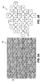
- FIG. 2 shows a portion of a pixel array 100 in the image sensor 20 of the digital camera of FIG. 1 in an illustrative embodiment.
- the CFA pattern is omitted from this plan view for clarity.
- the view shown is looking down on the upper surface of the sensor in the same direction in which the light 10 from the subject scene would be incident on that surface.
- the sensor is a stacked image sensor having a sensor wafer overlying a circuit wafer.
- the view of FIG. 2 therefore shows the upper surface of the sensor wafer.
- the sensor wafer comprises a plurality of photodiodes 102 arranged in respective positions of the two-dimensional array.
- positions of the array that would also normally include photodiodes in a conventional implementation do not include such elements in the present embodiment. Instead, these positions are utilized for shared diffusion regions 103 that are shared by multiple photodiodes in adjacent positions of the array.
- the array positions utilized for the shared diffusion regions 103 in this embodiment are examples of what are generally referred to herein as "dropped pixel" positions, as the corresponding pixel locations in the array do not include photodiodes.
- the particular sharing arrangement in the FIG. 2 embodiment is one in which a given diffusion region 103 is shared by four of the photodiodes 102.
- one of the diffusion regions 103 is shared by four photodiodes denoted A1, A2, A3 and A4. These four photodiodes occupy array positions adjacent to the array position that includes the corresponding shared diffusion region.
- the four photodiodes B1, B2, B3 and B4 share a common diffusion region, as do the four photodiodes C1, C2, C3 and C4, and the four photodiodes D1, D2, D3 and D4. This sharing arrangement is repeated with other sets of four photodiodes throughout the pixel array.
- the pixel array 100 of FIG. 2 comprises repeating groups of multiple array positions with a given such group comprising multiple positions that include respective photodiodes 102 and are arranged around a central position that does not include a photodiode but is instead utilized for a diffusion region 103 shared by the surrounding photodiodes.
- Each of the photodiodes that shares a given diffusion region 103 is coupled thereto via a corresponding transfer gate of the sensor wafer, as can be seen more clearly in FIGS. 3 and 4 .
- four photodiodes share a diffusion region in the FIG. 2 arrangement, other embodiments of the invention may utilize different sharing arrangements.
- FIGS. 5 , 6 and 7 Examples of arrangements in which six photodiodes share a given diffusion region and associated inter-wafer interconnect will be described below with reference to FIGS. 5 , 6 and 7 . Other examples with different sharing arrangements will be described with reference to FIGS. 8 and 9 .
- Each of the shared floating diffusion regions 103 of the sensor wafer as shown in FIG. 2 is associated with a corresponding inter-wafer interconnect 104 that serves to couple the sensor wafer to the underlying circuit wafer, as can be seen with reference to FIGS. 3 and 4 .
- the shared diffusion regions in the illustrative embodiments are assumed to be floating diffusion regions, but other types of diffusion regions, in any combination, may be used in alternative embodiments.
- a wide variety of diffusion region implementations are well known to those skilled in the art. See, for example, PCT International Publication No. WO 2006/130518 , entitled "CMOS Image Sensor Pixel with Selectable Binning".
- FIG. 3 shows a cross-sectional view of the pixel array 100 of FIG. 2 along the section line Z-Z' of the latter figure.
- CFA pattern 105 is formed on the upper surface of sensor wafer 106, and circuit wafer 108 underlies the sensor wafer 106.
- Light 10 from the subject scene is filtered by the CFA pattern 105 of the pixel array 100 such that designated portions of the visible spectrum are incident on respective ones of the photodiodes 102. For example, certain photodiodes may receive predominantly red, green or blue light, while others receive panchromatic light, in accordance with the particular CFA pattern that is utilized.
- each of four photodiodes 102 1 , 102 2 , 102 3 and 102 4 that share a common diffusion region 103 has an associated transfer gate 110.
- the diffusion region 103 of the sensor wafer 106 is illustratively a floating diffusion region.
- the four transfer gates 110 also denoted TG1, TG2, TG3 and TG4, couple the respective photodiodes to the shared diffusion region 103.
- This floating diffusion region is coupled via metal conductors 114, 115 of interconnect 104 to a corresponding floating diffusion region 116 in the circuit wafer 108.
- the floating diffusion regions 103, 116 of the sensor and circuit wafers are also denoted FD_SW and FD_CW, respectively.
- Metal conductors 114, 115 of interconnect 104 are located in the sensor and circuit wafers, respectively.
- the floating diffusion region 116 of the circuit wafer 108 is coupled to additional circuitry for processing signals generated by the photodiodes 102.
- This additional circuitry comprises a reset gate (RG) 120, a source follower (SF) 122, and a row select (RSEL) gate 124.
- This additional circuitry is coupled between a supply voltage VDD and an output voltage (VOUT) signal line 128.
- Each of the gates 110, 120, 122 and 124 in this embodiment is implemented as an N-type metal-oxide-semiconductor (NMOS) transistor, although other types of circuitry may be used, such as a P-type metal-oxide-semiconductor (PMOS) transistor. It is apparent from FIG.
- the circuit wafer includes a similar set of such circuitry for each of the sets of four photodiodes 102 in the sensor wafer that share a common floating diffusion region 103.
- the photodiodes A1, A3, B4, C2, D1 and D3 that lie along the section line Z-Z' in FIG. 2 are seen to be formed in silicon portion 130 of the sensor wafer 106. Also formed in this silicon portion of the sensor wafer is the floating diffusion region A, also denoted 103A, which is associated with the four photodiodes A1, A2, A3 and A4, and the floating diffusion region D, also denoted 103D, which is associated with the four photodiodes D1, D2, D3 and D4. It should be noted that the CFA pattern 105 in this embodiment has a black filter element over each of the floating diffusion regions 103A, 103D.
- such an arrangement serves to improve color uniformity for different pixels of the same color.
- the black filter elements may be eliminated, and the adjacent color filter elements extended over the floating diffusion regions 103A, 103D.
- Corresponding microlenses may be similarly extended. Arrangements of this type advantageously allow the neighboring photodiodes to "steal the light" from the corresponding dropped pixel positions of the pixel array, thereby improving sensitivity.
- a silicon portion 132 of the circuit wafer 108 includes corresponding floating diffusion regions A and D, also denoted 116A and 116D, respectively.
- the floating diffusion region 103A of the sensor wafer 106 is coupled via an interconnect 104A to the corresponding floating diffusion region 116A in the underlying circuit wafer 108.
- the interconnect 104A comprises metal conductors 114A formed in a metallization portion 140 of the sensor wafer and metal conductors 115A formed in a metallization portion 142 of the circuit wafer.
- the floating diffusion region 103D of the sensor wafer 106 is coupled via an interconnect 104D to a corresponding floating diffusion region 116D in the underlying circuit wafer 108.
- the interconnect 104D comprises metal conductors 114D formed in the metallization portion 140 of the sensor wafer 106 and metal conductors 115D formed in the metallization portion 142 of the circuit wafer 108.
- the metallization portion 140 of the sensor wafer comprises a single metal layer denoted "metal 1.”
- the metallization portion 142 of the circuit wafer 108 comprises multiple metal layers including layers denoted "metal 1" through “metal 8" as shown.
- the metal conductors 114, 115 of the inter-wafer interconnects 104 provide wafer-to-wafer electrical interconnection of the sensor and circuit wafers as indicated. It should be noted that the particular multi-layer metal interconnects shown in this example are not requirements of the invention. Numerous other types of inter-wafer interconnects may be used in alternative embodiments.
- row select gate 124 shown in the schematic diagram of FIG. 4 is omitted from the cross-sectional view of FIG. 3 for simplicity and clarity of illustration. Those skilled in the art will be familiar with the manner in which row select gates and other similar elements can be formed in a circuit wafer. In other embodiments, row select gates may be eliminated through the use of appropriate timing sequences that are known in the art.
- the dropped pixel positions that is, the array positions that do not include photodiodes but instead include shared diffusion regions, generally correspond to respective designated elements of the CFA pattern 105.
- FIGS. 5A and 5B a portion of the array 100 is shown, illustrating one possible implementation of the CFA pattern 105 as modified to include dropped pixel positions in accordance with an embodiment of the present invention.
- the CFA pattern in this example is a panchromatic checkerboard pattern of a type disclosed in the above-cited U.S. Patent Application Publication No. 2007/0024931 .
- FIG. 5A shows a larger portion of the pixel array 100
- FIG. 5B is a more detailed view of a smaller portion of the array as shown in FIG. 5A .
- the pixel array 100 as shown in these figures comprises a rectangular array of positions arranged in rows and columns.
- the array positions that include photodiodes are denoted as either red (R), green (G), blue (B) or panchromatic (P), in accordance with the corresponding elements of the particular CFA pattern 105.
- the array positions that do not include photodiodes, referred to as the dropped pixel positions of the array, are identified in FIG. 5A by an "x.”
- the pixel array 100 implements a four-pixel sharing arrangement in which four of the array positions that include photodiodes are arranged around a single central dropped pixel position, with the dropped pixel position being utilized for a diffusion region shared by the four photodiodes.
- This exemplary sharing arrangement is more clearly shown in FIG. 5B , where it can be seen that one of the dropped pixel positions 150-1 is associated with four surrounding panchromatic pixels.
- Another of the dropped pixel positions 150-2 is associated with two pairs of same-color pixels, with the same-color pixels of a given one of the pairs being arranged on opposite sides of that dropped pixel position. More specifically, dropped pixel position 150-2 is associated with a pair of blue pixels and a pair of green pixels.
- Other groups of array positions in the array 100 are configured in a similar manner, to include either four panchromatic pixels around a dropped pixel position, or two different pairs of same-color pixels arranged around a dropped pixel position.
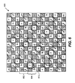
- FIG. 6 Another example is shown in FIG. 6 , where a pixel array 600 has a different panchromatic checkerboard CFA pattern than that used in FIG. 5 , and utilizes a six-pixel sharing arrangement rather than the four-pixel sharing arrangement of FIGS. 2 through 5 .
- the array 600 comprises blue/green row pairs 602 which include only blue, green and panchromatic pixels.
- the blue/green row pairs 602 alternate with red/green row pairs 604 that include only red, green and panchromatic pixels.
- 6 example comprises 16 contiguous pixels and may be viewed as being arranged as follows: PBPG BPGP PGPR GPRP Patterns with other minimal repeating units, such as minimal repeating units of at least 12 pixels as described in the above-cited U.S. Patent Application Publication No. 2007/0024931 , may be used. Also, colors other than red, green and blue may be used, such as, for example, cyan, magenta and yellow.
- a given group of array positions in this example comprises six positions that include photodiodes arranged around a single central dropped pixel position 610 that does not include a photodiode but instead includes a shared diffusion region.
- the location of the dropped pixel position varies in a regular manner from row to row within the pixel array 600. More specifically, in this example, every eighth pixel position in a given row is a dropped pixel position, and the dropped pixel positions are offset from row to row by two pixel positions. The dropped pixel positions thus also follow a repeating pattern within the array.
- the six pixels which share a diffusion region in a given dropped pixel position are shown in FIG. 6 as being interconnected with one another. This shared diffusion region is assumed to be coupled to a corresponding region in an underlying circuit wafer via a corresponding inter-wafer interconnect, as in the embodiment of FIGS. 2 to 5 .
- the pixel array comprises a rectangular array of rows and columns.
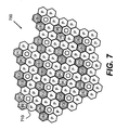
- FIG. 7 shows an alternative embodiment in which the pixel array of image sensor 20 is not a rectangular array, but is instead a hexagonal array.
- a pixel array 700 again comprises repeating groups of array positions with a given such group comprising multiple positions that include respective photodiodes and are arranged around a single central dropped pixel position that does not include a photodiode but is instead utilized for a diffusion region shared by the surrounding photodiodes.
- each group in this embodiment comprises six positions that include photodiodes and are arranged around a single central dropped pixel position 710 that does not include a photodiode.
- each of the photodiodes in the group is coupled via a corresponding transfer gate to a shared diffusion region arranged in the dropped pixel position. Again, this shared diffusion region is assumed to be coupled to a corresponding region in an underlying circuit wafer via a corresponding inter-wafer interconnect, as in the embodiment of FIGS. 2 to 5 .
- the photodiodes in two adjacent ones of the six positions that include photodiodes comprise same-color photodiodes in accordance with the CFA pattern associated with the image sensor, while the photodiodes in the remaining ones of the six positions comprise panchromatic photodiodes in accordance with the CFA pattern.
- the uppermost group at the left hand side of the pixel array 700 includes two adjacent red pixels and four panchromatic pixels arranged around the dropped pixel position 710.
- Other groups of positions in the pixel array are similarly configured to include two adjacent same-color pixels, which may be either red, green or blue, and four adjacent panchromatic pixels, surrounding a dropped pixel position. This particular arrangement facilitates color binning. Also, since each pair of same-color pixels is completely surrounded by panchromatic pixels, CFA interpolation operations can be performed more easily and accurately. Again, the particular CFA pattern and the pixel sharing arrangement may be varied in other embodiments.
- pixel arrays can be classified geometrically as plane tilings by regular polygons.
- the tiling may be viewed as being generated from a single polygon, namely a square, while in the example of FIG. 7 the tiling is also generated from a single polygon, but in this case a hexagon.
- the corresponding patterns are generally referred to as a square tiling pattern and a hexagonal tiling pattern, respectively.
- the dropped pixel positions of the pixel array correspond to selected ones of the tiles of the tiling pattern.
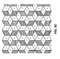
- FIG. 8 illustrates another embodiment of the invention.
- a pixel array 800 having a hexagonal tiling pattern is shown.
- the dropped pixel positions in this array are denoted by the letter D.
- Reference numeral 810 denotes a particular one of the dropped pixel positions.
- one in four of the hexagons of the hexagonal tiling pattern is identified as a dropped pixel position.
- FIG. 8B shows a plan view of the pixel array 800, with each dropped pixel position including a floating diffusion region that is shared by photodiodes in three neighboring pixel positions via respective transfer gates.
- the photodiodes may be viewed as having a quasiregular rhombic tiling.
- FIG. 8C shows an example of a CFA pattern that may be used for the quasiregular rhombic tiling of FIG. 8B .
- the red, green and blue color filter elements are grouped in pairs of two same-color elements so that they can be binned for better luminance matching.
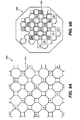
- FIG. 9 illustrates yet another embodiment of the invention.
- the tiling pattern in this embodiment is a type of truncated square tiling pattern, shown generally in FIG. 9A .
- This truncated square tiling pattern is generated from two polygons, namely, a square and an octagon.
- the dropped pixel positions in the pixel array 900 are again denoted by the letter D, and generally correspond to half of the square polygons.
- Reference numeral 910 denotes a particular one of the dropped pixel positions.
- FIG. 9B shows a plan view of the pixel array 900, with each dropped pixel position including a floating diffusion region that is shared by photodiodes in two neighboring pixel positions via respective transfer gates.
- tiling arrangements may be used in implementing an image sensor in accordance with the invention.
- Other examples include rows with square unit cells, rows with rectangular unit cells, trihexagonal tiling, snub hexagonal tiling, prismatic pentagonal tiling, Cairo pentagonal tiling, truncated hexagonal tiling, snub square tiling, floret pentagonal tiling, etc.
- Those skilled in the art will recognize that the disclosed techniques can be adapted in a straightforward manner to these and other types of pixel arrays.
- the illustrative embodiments facilitate the interconnection of sensor and circuit wafers in a stacked image sensor, thereby reducing sensor cost and complexity.
- These embodiments leverage the advantages of sparse CFA patterns for increased low light sensitivity.
- configuring the dropped pixel positions in a regular repeating pattern subsequent image processing operations are simplified.
Description
- The present invention relates generally to electronic image sensors for use in digital cameras and other image capture devices, and more particularly to image sensors comprising sensor and circuit wafers arranged in a stack.
- A typical electronic image sensor comprises a number of light sensitive picture elements ("pixels") arranged in a two-dimensional array. Such an image sensor may be configured to produce a color image by forming a color filter array (CFA) over the pixels. One commonly used type of CFA pattern is the Bayer pattern, disclosed in
U.S. Patent No. 3,971,065 , entitled "Color Imaging Array". The Bayer CFA pattern provides each pixel with color photoresponse exhibiting a predominant sensitivity to one of three designated portions of the visible spectrum. The three designated portions may be, for example, red, green and blue, or cyan, magenta and yellow. A given CFA pattern is generally characterized by a minimal repeating unit in the form of a subarray of contiguous pixels that acts as a basic building block for the pattern. Multiple copies of the minimal repeating unit are juxtaposed to form the complete pattern. - An image captured using an image sensor with a Bayer CFA pattern has only one color value at each pixel. Therefore, in order to produce a full color image, the missing color values at each pixel are interpolated from the color values of nearby pixels. Numerous such interpolation techniques are known in the art. See, for example,
U.S. Patent No. 5,652,621 , entitled "Adaptive Color Plane Interpolation in Single Sensor Color Electronic Camera". - It is known to form a given image sensor as a so-called stacked image sensor. In a typical arrangement of this type, photodiodes or other photosensitive elements of the pixel array are formed in a first semiconductor die or layer, while associated circuitry for processing signals from the photosensitive elements is formed in a second semiconductor die or layer that underlies the first semiconductor die or layer. These first and second semiconductor die or layers are examples of what are more generally referred to herein as sensor and circuit wafers, respectively.
- A problem that arises in conventional stacked image sensors relates to the manner in which the photosensitive elements in the sensor wafer are interconnected with the associated circuitry in the circuit wafer. The typical conventional approach generally calls for such interconnects to be formed on a per-pixel basis, that is, with a separate inter-wafer interconnect provided for each pixel. It is clear that such an approach can significantly increase the cost and complexity of the stacked image sensor. It can also have a negative impact on sensor performance.
- Accordingly, a need exists for an improved stacked image sensor which overcomes the above-noted drawbacks of conventional practice.
-
EP 1453097 discloses a solid-state image sensor and its production method. The solid-state image sensor has a chip-size package, which can be easily fabricated. -
US 2008/0062290 discloses a color image sensor including an array of pixels arranged in a plurality of pixel groups, each pixel group including a floating diffusion that is shared by four pixels disposed in a 2x2 arrangement. -
US 2007/018073 discloses a CMOS image sensor cell including a first pixel area in which at least one first photodiode is disposed for generating a first sense signal in response to a photo-signal of a first color; a second pixel area neighboring the first pixel area, in which at least one second photodiode is disposed for generating a second sense signal in response to a photo-signal of the second color; and a third pixel area neighboring the first and second pixel areas, in which at least one third photodiode is disposed for generating a third sense signal in response to a photo-signal of a third color. -
US2007/0210239 discloses an image sensor comprising an array of photoelectric conversion elements in a substrate, the photoelectric conversion element being arranged in rows and columns extending in a first direction and a second direction respectively; a plurality of first junction isolation regions in the substrate that each isolate side portions of neighboring photoelectric conversion elements of a common row, and a plurality of second junction isolation regions in the substrate that each isolate side portions of neighboring photoelectric conversion elements of a common column; and a plurality of dialelectric isolation regions in the substrate, that each isolate corner portions of neighboring photoelectric conversion elements. -
US 2007/0215912 discloses a solid-state imaging device. In the solid-state imaging device, plural unit areas, each having a photoelectric conversion region converting incident light into electric signals are provided adjacently, which each photoelectric conversion region is provided being deviated from the central position of each unit area to a boundary position between the plural unit areas, a high refractive index material layer is arranged over the deviated photoelectric conversion region, and a low refractive index material layer is provided over the photoelectric conversion regions at the inverse side of the deviated direction being adjacent to the high refractive index material layer, and optical paths of the incident light are changed by the high refractive index material layer and the low refractive index material layer, and the incident light enters the photoelectic conversion region. - The invention provides an image sensor as set out in
claim 1 and a method as set out in claim 15. - Illustrative embodiments of the invention provide stacked image sensors in which shared diffusion regions are arranged in designated array positions that would normally include photosensitive elements. The techniques of the invention generally involve dropping the photosensitive elements from these designated array positions and instead utilizing the positions to facilitate the formation of diffusion regions that are shared by multiple photosensitive elements in adjacent positions of the array.
- In accordance with one aspect of the invention, an image sensor comprises a sensor wafer and an underlying circuit wafer. The sensor wafer comprises a plurality of photodiodes or other photosensitive elements arranged in respective positions of a two-dimensional array of positions in which a subset of the array positions do not include photosensitive elements but instead include diffusion regions each of which is shared by two or more of the photosensitive elements. The diffusion regions may be, for example, floating diffusion regions. The sensor wafer is interconnected with the circuit wafer utilizing a plurality of inter-wafer interconnects coupled to respective ones of the shared diffusion regions in respective ones of the array positions that do not include photosensitive elements.
- The two-dimensional array comprises repeating groups of multiple positions with a given such group comprising a plurality of positions that include photosensitive elements arranged around a central dropped pixel position that does not include a photosensitive element. A given one of the shared diffusion regions is arranged in the central position of the given group and is shared by the photosensitive elements in at least a subset of the positions arranged around that central position. Each of the photosensitive elements that shares a given one of the shared diffusion regions may be coupled to that shared diffusion region via a corresponding transfer gate of the sensor wafer.
- In one of the illustrative embodiment, the array of positions comprises a rectangular array of rows and columns of positions. For example, the given group may comprise four positions that include photosensitive elements and are arranged around a single central dropped pixel position that does not include a photosensitive element but instead includes one of the shared diffusion regions. The photosensitive elements in the four positions that include photosensitive elements may be panchromatic elements in accordance with a CFA pattern of the image sensor, or may comprise same-color pairs of two different colors of the CFA pattern. As another example, the given group may comprise six positions that include photosensitive elements and are arranged around a single central dropped pixel position that does not include a photosensitive element but instead includes one of the shared diffusion regions.
- Other embodiments of the invention need not include rectangular arrays but may instead include arrays in other shapes, such as hexagonal arrays. For example, the given group referred to above in the case of a hexagonal array may also comprise six positions that include photosensitive elements and are arranged around a single central dropped pixel position that does not include a photosensitive element but instead includes one of the shared diffusion regions. However, in this case, the photosensitive elements in two adjacent ones of the six positions that include photosensitive elements are same-color elements, while the remaining ones of the six positions are panchromatic elements.
- An image sensor in accordance with the invention may be advantageously implemented in a digital camera or other type of image capture device. The techniques disclosed herein considerably facilitate the manufacture of stacked image sensors, at reduced cost and complexity, particularly for those image sensors having sparse CFA patterns.
- The above and other objects, features, and advantages of the present invention will become more apparent when taken in conjunction with the following description and drawings wherein identical reference numerals have been used, where possible, to designate identical features that are common to the figures, and wherein:
-
FIG. 1 is a block diagram of a digital camera having a stacked image sensor with a sparse CFA pattern and incorporating shared diffusion regions and associated inter-wafer interconnects in accordance with an illustrative embodiment of the invention; -
FIG. 2 is a plan view showing a portion of a pixel array in the image sensor of the digital camera ofFIG. 1 ; -
FIG. 3 is a cross-sectional view of the portion of the pixel array ofFIG. 2 illustrating shared diffusion regions and associated inter-wafer interconnects; -
FIG. 4 is a schematic diagram illustrating the manner in which a given diffusion region of the pixel array ofFIGS. 2 and3 is shared by four photodiodes of that array; -
FIGS. 5A and 5B illustrate the manner in which particular dropped pixel positions correspond to respective elements of an exemplary CFA pattern that may be utilized with the pixel array ofFIGS. 2 and3 ; and -
FIGS. 6 through 9B show other examples of pixel arrays with shared diffusion regions and associated inter-wafer interconnects in illustrative embodiments of the invention. - The present invention will be illustrated herein in conjunction with particular embodiments of image capture devices and image sensors. It should be understood, however, that these illustrative arrangements are presented by way of example only, and should not be viewed as limiting the scope of the invention in any way. Those skilled in the art will recognize that the disclosed arrangements can be adapted in a straightforward manner for use with a wide variety of other types of image capture devices and image sensors.
-
FIG. 1 shows a digital camera in which an image sensor having shared inter-wafer interconnects is implemented in an illustrative embodiment of the invention. In the digital camera,light 10 from a subject scene is input to animaging stage 11. Theimaging stage 11 compriseslens 12, neutral density (ND)filter 13,iris 14 andshutter 18. The light 10 is focused bylens 12 to form an image on animage sensor 20. The amount of light reaching theimage sensor 20 is regulated byiris 14,ND filter 13 and the time that shutter 18 is open.Image sensor 20 converts the incident light to an electrical signal for each pixel. Theimage sensor 20 may be, for example, a charge coupled device (CCD) type or active pixel sensor (APS) type image sensor, although other types of image sensors may be used in implementing the invention. APS type image sensors fabricated using a complementary metal-oxide-semiconductor (CMOS) process are often referred to as CMOS image sensors. - The
image sensor 20 generally has a two-dimensional array of pixels configured in accordance with a designated CFA pattern. Examples of CFA patterns that may be used with theimage sensor 20 include the panchromatic checkerboard patterns disclosed inU.S. Patent Application Publication No. 2007/0024931 , entitled "Image Sensor with Improved Light Sensitivity". These panchromatic checkerboard patterns provide certain of the pixels with a panchromatic photoresponse, and are also generally referred to herein as "sparse" CFA patterns. A panchromatic photoresponse has a wider spectral sensitivity than those spectral sensitivities represented in the selected set of color photoresponses and may, for example, have high sensitivity across substantially the entire visible spectrum. Image sensors configured with panchromatic checkerboard CFA patterns exhibit greater light sensitivity and are thus well-suited for use in applications involving low scene lighting, short exposure time, small aperture, or other restrictions on the amount of light reaching the image sensor. Other types of CFA patterns may be used in other embodiments of the invention. - An analog signal from
image sensor 20 is processed byanalog signal processor 22 and applied to analog to digital (A/D)converter 24. Timinggenerator 26 produces various clocking signals to select particular rows and columns of the pixel array for processing, and synchronizes the operation ofanalog signal processor 22 and A/D converter 24. Theimage sensor 20,analog signal processor 22, A/D converter 24, andtiming generator 26 collectively form animage sensor stage 28 of the digital camera. The components ofimage sensor stage 28 may comprise separately fabricated integrated circuits, or they may be fabricated as a single integrated circuit as is commonly done with CMOS image sensors. The A/D converter 24 outputs a stream of digital pixel values that are supplied via a bus 30 to a memory 32 associated with a digital signal processor (DSP) 36. Memory 32 may comprise any type of memory, such as, for example, synchronous dynamic random access memory (SDRAM). The bus 30 provides a pathway for address and data signals and connects DSP 36 to memory 32 and A/D converter 24. - The DSP 36 is one of a plurality of processing elements of the digital camera that are indicated as collectively comprising a processing stage 38. The other processing elements of the processing stage 38 include
exposure controller 40 andsystem controller 50. Although this partitioning of digital camera functional control among multiple processing elements is typical, these elements may be combined in various ways without affecting the functional operation of the camera and the application of the present invention. A given one of the processing elements of processing stage 38 can comprise one or more DSP devices, microcontrollers, programmable logic devices, or other digital logic circuits. Although a combination of three separate processing elements is shown in the figure, alternative embodiments may combine the functionality of two or more of these elements into a single processor, controller or other processing element. Techniques for sampling and readout of the pixel array of theimage sensor 20 may be implemented at least in part in the form of software that is executed by one or more such processing elements. - The
exposure controller 40 is responsive to an indication of an amount of light available in the scene, as determined bybrightness sensor 42, and provides appropriate control signals to theND filter 13,iris 14 and shutter 18 of theimaging stage 11. - The
system controller 50 is coupled via abus 52 to DSP 36 and to programmemory 54,system memory 56,host interface 57 andmemory card interface 60. Thesystem controller 50 controls the overall operation of the digital camera based on one or more software programs stored inprogram memory 54, which may comprise Flash electrically erasable programmable read-only memory (EEPROM) or other nonvolatile memory. This memory is also used to store image sensor calibration data, user setting selections and other data which must be preserved when the camera is turned off.System controller 50 controls the sequence of image capture by directingexposure controller 40 to operate thelens 12,ND filter 13,iris 14, and shutter 18 as previously described, directing thetiming generator 26 to operate theimage sensor 20 and associated elements, and directing DSP 36 to process the captured image data. - In the illustrated embodiment, DSP 36 manipulates the digital image data in its memory 32 according to one or more software programs stored in
program memory 54 and copied to memory 32 for execution during image capture. After an image is captured and processed, the resulting image file stored in memory 32 may be, for example, transferred viahost interface 57 to an external host computer, transferred viamemory card interface 60 andmemory card socket 62 toremovable memory card 64, or displayed for the user on animage display 65. Theimage display 65 is typically an active matrix color liquid crystal display (LCD), although other types of displays may be used. - The digital camera further comprises a user control and
status interface 68 including aviewfinder display 70, an exposure display 72, user inputs 74 andstatus display 76. These elements may be controlled by a combination of software programs executed onexposure controller 40 andsystem controller 50. The user inputs 74 typically include some combination of buttons, rocker switches, joysticks, rotary dials or touchscreens.Exposure controller 40 operates light metering, exposure mode, autofocus and other exposure functions. Thesystem controller 50 manages a graphical user interface (GUI) presented on one or more of the displays, e.g., onimage display 65. The GUI typically includes menus for making various option selections and review modes for examining captured images. - Processed images may be copied to a display buffer in
system memory 56 and continuously read out viavideo encoder 80 to produce a video signal. This signal may be output directly from the camera for display on an external monitor, or processed bydisplay controller 82 and presented onimage display 65. - It is to be appreciated that the digital camera as shown in
FIG. 1 may comprise additional or alternative elements of a type known to those skilled in the art. Elements not specifically shown or described herein may be selected from those known in the art. As noted previously, the present invention may be implemented in a wide variety of other types of digital cameras or image capture devices. For example, the present invention can be implemented in imaging applications involving mobile phones and automotive vehicles. Also, as mentioned above, certain aspects of the embodiments described herein may be implemented at least in part in the form of software executed by one or more processing elements of an image capture device. Such software can be implemented in a straightforward manner given the teachings provided herein, as will be appreciated by those skilled in the art. - The two-dimensional pixel array of
image sensor 20 comprises an array of light sensitive pixels, fabricated using stacked sensor and circuit wafers, that provide a way of converting incoming light at each pixel into an electrical signal that is measured. As the sensor is exposed to light, free carriers are generated and captured within the photosensitive element at each pixel. Capturing these free carriers for some period of time and then measuring the number of carriers captured, or measuring the rate at which free carriers are generated, allows the light level at each pixel to be measured. In the former case, accumulated carriers may be shifted out of a given photosensitive element and onto an input node of a charge to voltage measurement circuit as in a CMOS image sensor. - Sampling and readout circuitry in a given embodiment may encompass switches or other elements that are formed integrally with the pixel array. Such sampling and readout circuitry is generally implemented within the
sensor array 20, for example, as in the case of a CMOS image sensor. - Whenever general reference is made to an image sensor in the following description, it is understood to be representative of the
image sensor 20 fromFIG. 1 . It is further understood that all examples and their equivalents of image sensor architectures and pixel patterns of the present invention disclosed in this specification are used forimage sensor 20. - In the context of an image sensor, a pixel may refer to a discrete light sensing area and charge shifting or charge measurement circuitry associated with the light sensing area. In the context of a digital color image, the term pixel commonly refers to a particular location in the image having associated color values.
-
FIG. 2 shows a portion of apixel array 100 in theimage sensor 20 of the digital camera ofFIG. 1 in an illustrative embodiment. It should be noted that the CFA pattern is omitted from this plan view for clarity. Generally, the view shown is looking down on the upper surface of the sensor in the same direction in which the light 10 from the subject scene would be incident on that surface. It is assumed that the sensor is a stacked image sensor having a sensor wafer overlying a circuit wafer. The view ofFIG. 2 therefore shows the upper surface of the sensor wafer. It can be seen that the sensor wafer comprises a plurality ofphotodiodes 102 arranged in respective positions of the two-dimensional array. However, certain positions of the array that would also normally include photodiodes in a conventional implementation do not include such elements in the present embodiment. Instead, these positions are utilized for shareddiffusion regions 103 that are shared by multiple photodiodes in adjacent positions of the array. The array positions utilized for the shareddiffusion regions 103 in this embodiment are examples of what are generally referred to herein as "dropped pixel" positions, as the corresponding pixel locations in the array do not include photodiodes. - The particular sharing arrangement in the
FIG. 2 embodiment is one in which a givendiffusion region 103 is shared by four of thephotodiodes 102. For example, one of thediffusion regions 103 is shared by four photodiodes denoted A1, A2, A3 and A4. These four photodiodes occupy array positions adjacent to the array position that includes the corresponding shared diffusion region. Similarly, the four photodiodes B1, B2, B3 and B4 share a common diffusion region, as do the four photodiodes C1, C2, C3 and C4, and the four photodiodes D1, D2, D3 and D4. This sharing arrangement is repeated with other sets of four photodiodes throughout the pixel array. - Thus, it is apparent that the
pixel array 100 ofFIG. 2 comprises repeating groups of multiple array positions with a given such group comprising multiple positions that includerespective photodiodes 102 and are arranged around a central position that does not include a photodiode but is instead utilized for adiffusion region 103 shared by the surrounding photodiodes. Each of the photodiodes that shares a givendiffusion region 103 is coupled thereto via a corresponding transfer gate of the sensor wafer, as can be seen more clearly inFIGS. 3 and4 . Although four photodiodes share a diffusion region in theFIG. 2 arrangement, other embodiments of the invention may utilize different sharing arrangements. Examples of arrangements in which six photodiodes share a given diffusion region and associated inter-wafer interconnect will be described below with reference toFIGS. 5 ,6 and7 . Other examples with different sharing arrangements will be described with reference toFIGS. 8 and9 . - Each of the shared floating
diffusion regions 103 of the sensor wafer as shown inFIG. 2 is associated with a correspondinginter-wafer interconnect 104 that serves to couple the sensor wafer to the underlying circuit wafer, as can be seen with reference toFIGS. 3 and4 . The shared diffusion regions in the illustrative embodiments are assumed to be floating diffusion regions, but other types of diffusion regions, in any combination, may be used in alternative embodiments. A wide variety of diffusion region implementations are well known to those skilled in the art. See, for example, PCT International Publication No.WO 2006/130518 , entitled "CMOS Image Sensor Pixel with Selectable Binning". -
FIG. 3 shows a cross-sectional view of thepixel array 100 ofFIG. 2 along the section line Z-Z' of the latter figure. In this view, it can be seen thatCFA pattern 105 is formed on the upper surface ofsensor wafer 106, andcircuit wafer 108 underlies thesensor wafer 106.Light 10 from the subject scene is filtered by theCFA pattern 105 of thepixel array 100 such that designated portions of the visible spectrum are incident on respective ones of thephotodiodes 102. For example, certain photodiodes may receive predominantly red, green or blue light, while others receive panchromatic light, in accordance with the particular CFA pattern that is utilized. - As shown in the schematic diagram of
FIG. 4 , each of fourphotodiodes common diffusion region 103 has an associatedtransfer gate 110. Thediffusion region 103 of thesensor wafer 106 is illustratively a floating diffusion region. The fourtransfer gates 110, also denoted TG1, TG2, TG3 and TG4, couple the respective photodiodes to the shareddiffusion region 103. This floating diffusion region is coupled viametal conductors interconnect 104 to a corresponding floatingdiffusion region 116 in thecircuit wafer 108. The floatingdiffusion regions Metal conductors interconnect 104 are located in the sensor and circuit wafers, respectively. - The floating
diffusion region 116 of thecircuit wafer 108 is coupled to additional circuitry for processing signals generated by thephotodiodes 102. This additional circuitry comprises a reset gate (RG) 120, a source follower (SF) 122, and a row select (RSEL)gate 124. This additional circuitry is coupled between a supply voltage VDD and an output voltage (VOUT)signal line 128. Each of thegates FIG. 4 that the set of additionalcircuitry comprising gates circuit wafer 108 is shared by the fourphotodiodes sensor wafer 106. The circuit wafer includes a similar set of such circuitry for each of the sets of fourphotodiodes 102 in the sensor wafer that share a common floatingdiffusion region 103. - Returning to the cross-sectional view of
FIG. 3 , the photodiodes A1, A3, B4, C2, D1 and D3 that lie along the section line Z-Z' inFIG. 2 are seen to be formed insilicon portion 130 of thesensor wafer 106. Also formed in this silicon portion of the sensor wafer is the floating diffusion region A, also denoted 103A, which is associated with the four photodiodes A1, A2, A3 and A4, and the floating diffusion region D, also denoted 103D, which is associated with the four photodiodes D1, D2, D3 and D4. It should be noted that theCFA pattern 105 in this embodiment has a black filter element over each of the floatingdiffusion regions diffusion regions - A
silicon portion 132 of thecircuit wafer 108 includes corresponding floating diffusion regions A and D, also denoted 116A and 116D, respectively. The floatingdiffusion region 103A of thesensor wafer 106 is coupled via aninterconnect 104A to the corresponding floating diffusion region 116A in theunderlying circuit wafer 108. Theinterconnect 104A comprisesmetal conductors 114A formed in ametallization portion 140 of the sensor wafer andmetal conductors 115A formed in ametallization portion 142 of the circuit wafer. - Similarly, the floating
diffusion region 103D of thesensor wafer 106 is coupled via aninterconnect 104D to a corresponding floating diffusion region 116D in theunderlying circuit wafer 108. Theinterconnect 104D comprisesmetal conductors 114D formed in themetallization portion 140 of thesensor wafer 106 andmetal conductors 115D formed in themetallization portion 142 of thecircuit wafer 108. Themetallization portion 140 of the sensor wafer comprises a single metal layer denoted "metal 1." Themetallization portion 142 of thecircuit wafer 108 comprises multiple metal layers including layers denoted "metal 1" through "metal 8" as shown. Themetal conductors inter-wafer interconnects 104 provide wafer-to-wafer electrical interconnection of the sensor and circuit wafers as indicated. It should be noted that the particular multi-layer metal interconnects shown in this example are not requirements of the invention. Numerous other types of inter-wafer interconnects may be used in alternative embodiments. - Also formed in the
silicon portion 132 of thecircuit wafer 108 are parts of thereset gate 120 andsource follower 122 for each of the groups A and D of photodiodes. It should be noted that the rowselect gate 124 shown in the schematic diagram ofFIG. 4 is omitted from the cross-sectional view ofFIG. 3 for simplicity and clarity of illustration. Those skilled in the art will be familiar with the manner in which row select gates and other similar elements can be formed in a circuit wafer. In other embodiments, row select gates may be eliminated through the use of appropriate timing sequences that are known in the art. - The dropped pixel positions, that is, the array positions that do not include photodiodes but instead include shared diffusion regions, generally correspond to respective designated elements of the
CFA pattern 105. - With reference now to
FIGS. 5A and 5B , a portion of thearray 100 is shown, illustrating one possible implementation of theCFA pattern 105 as modified to include dropped pixel positions in accordance with an embodiment of the present invention. The CFA pattern in this example is a panchromatic checkerboard pattern of a type disclosed in the above-citedU.S. Patent Application Publication No. 2007/0024931 .FIG. 5A shows a larger portion of thepixel array 100, whileFIG. 5B is a more detailed view of a smaller portion of the array as shown inFIG. 5A . Thepixel array 100 as shown in these figures comprises a rectangular array of positions arranged in rows and columns. The array positions that include photodiodes are denoted as either red (R), green (G), blue (B) or panchromatic (P), in accordance with the corresponding elements of theparticular CFA pattern 105. The array positions that do not include photodiodes, referred to as the dropped pixel positions of the array, are identified inFIG. 5A by an "x." - As previously described in conjunction with
FIGS. 2 through 4 , thepixel array 100 implements a four-pixel sharing arrangement in which four of the array positions that include photodiodes are arranged around a single central dropped pixel position, with the dropped pixel position being utilized for a diffusion region shared by the four photodiodes. This exemplary sharing arrangement is more clearly shown inFIG. 5B , where it can be seen that one of the dropped pixel positions 150-1 is associated with four surrounding panchromatic pixels. Another of the dropped pixel positions 150-2 is associated with two pairs of same-color pixels, with the same-color pixels of a given one of the pairs being arranged on opposite sides of that dropped pixel position. More specifically, dropped pixel position 150-2 is associated with a pair of blue pixels and a pair of green pixels. Other groups of array positions in thearray 100 are configured in a similar manner, to include either four panchromatic pixels around a dropped pixel position, or two different pairs of same-color pixels arranged around a dropped pixel position. - It is to be appreciated that the particular sparse CFA pattern and pixel sharing arrangement used in the four-shared
pixel array 100 as shown inFIG. 5 is exemplary only, and numerous other types of CFA patterns and sharing arrangements may be used. - Another example is shown in
FIG. 6 , where apixel array 600 has a different panchromatic checkerboard CFA pattern than that used inFIG. 5 , and utilizes a six-pixel sharing arrangement rather than the four-pixel sharing arrangement ofFIGS. 2 through 5 . Thearray 600 comprises blue/green row pairs 602 which include only blue, green and panchromatic pixels. The blue/green row pairs 602 alternate with red/green row pairs 604 that include only red, green and panchromatic pixels. The minimal repeating unit in the particular CFA pattern used in theFIG. 6 example comprises 16 contiguous pixels and may be viewed as being arranged as follows:PBPG BPGP PGPR GPRP U.S. Patent Application Publication No. 2007/0024931 , may be used. Also, colors other than red, green and blue may be used, such as, for example, cyan, magenta and yellow. - A given group of array positions in this example comprises six positions that include photodiodes arranged around a single central dropped
pixel position 610 that does not include a photodiode but instead includes a shared diffusion region. The location of the dropped pixel position varies in a regular manner from row to row within thepixel array 600. More specifically, in this example, every eighth pixel position in a given row is a dropped pixel position, and the dropped pixel positions are offset from row to row by two pixel positions. The dropped pixel positions thus also follow a repeating pattern within the array. The six pixels which share a diffusion region in a given dropped pixel position are shown inFIG. 6 as being interconnected with one another. This shared diffusion region is assumed to be coupled to a corresponding region in an underlying circuit wafer via a corresponding inter-wafer interconnect, as in the embodiment ofFIGS. 2 to 5 . - In the embodiments of
FIGS. 2 through 6 , the pixel array comprises a rectangular array of rows and columns. However, other embodiments of the invention need not utilize a rectangular array. For example,FIG. 7 shows an alternative embodiment in which the pixel array ofimage sensor 20 is not a rectangular array, but is instead a hexagonal array. In this embodiment, apixel array 700 again comprises repeating groups of array positions with a given such group comprising multiple positions that include respective photodiodes and are arranged around a single central dropped pixel position that does not include a photodiode but is instead utilized for a diffusion region shared by the surrounding photodiodes. More specifically, each group in this embodiment comprises six positions that include photodiodes and are arranged around a single central droppedpixel position 710 that does not include a photodiode. As in the previous embodiments, each of the photodiodes in the group is coupled via a corresponding transfer gate to a shared diffusion region arranged in the dropped pixel position. Again, this shared diffusion region is assumed to be coupled to a corresponding region in an underlying circuit wafer via a corresponding inter-wafer interconnect, as in the embodiment ofFIGS. 2 to 5 . - The photodiodes in two adjacent ones of the six positions that include photodiodes comprise same-color photodiodes in accordance with the CFA pattern associated with the image sensor, while the photodiodes in the remaining ones of the six positions comprise panchromatic photodiodes in accordance with the CFA pattern. For example, the uppermost group at the left hand side of the
pixel array 700 includes two adjacent red pixels and four panchromatic pixels arranged around the droppedpixel position 710. Other groups of positions in the pixel array are similarly configured to include two adjacent same-color pixels, which may be either red, green or blue, and four adjacent panchromatic pixels, surrounding a dropped pixel position. This particular arrangement facilitates color binning. Also, since each pair of same-color pixels is completely surrounded by panchromatic pixels, CFA interpolation operations can be performed more easily and accurately. Again, the particular CFA pattern and the pixel sharing arrangement may be varied in other embodiments. - It is apparent from the foregoing description that pixel arrays can be classified geometrically as plane tilings by regular polygons. In the examples of
FIGS. 2 through 6 , the tiling may be viewed as being generated from a single polygon, namely a square, while in the example ofFIG. 7 the tiling is also generated from a single polygon, but in this case a hexagon. The corresponding patterns are generally referred to as a square tiling pattern and a hexagonal tiling pattern, respectively. The dropped pixel positions of the pixel array correspond to selected ones of the tiles of the tiling pattern. -
FIG. 8 illustrates another embodiment of the invention. With reference toFIG. 8A , apixel array 800 having a hexagonal tiling pattern is shown. The dropped pixel positions in this array are denoted by the letter D. Reference numeral 810 denotes a particular one of the dropped pixel positions. In this embodiment, one in four of the hexagons of the hexagonal tiling pattern is identified as a dropped pixel position.FIG. 8B shows a plan view of thepixel array 800, with each dropped pixel position including a floating diffusion region that is shared by photodiodes in three neighboring pixel positions via respective transfer gates. The photodiodes may be viewed as having a quasiregular rhombic tiling.FIG. 8C shows an example of a CFA pattern that may be used for the quasiregular rhombic tiling ofFIG. 8B . The red, green and blue color filter elements are grouped in pairs of two same-color elements so that they can be binned for better luminance matching. -
FIG. 9 illustrates yet another embodiment of the invention. The tiling pattern in this embodiment is a type of truncated square tiling pattern, shown generally inFIG. 9A . This truncated square tiling pattern is generated from two polygons, namely, a square and an octagon. The dropped pixel positions in thepixel array 900 are again denoted by the letter D, and generally correspond to half of the square polygons.Reference numeral 910 denotes a particular one of the dropped pixel positions.FIG. 9B shows a plan view of thepixel array 900, with each dropped pixel position including a floating diffusion region that is shared by photodiodes in two neighboring pixel positions via respective transfer gates. - Of course, numerous other tiling arrangements may be used in implementing an image sensor in accordance with the invention. Other examples include rows with square unit cells, rows with rectangular unit cells, trihexagonal tiling, snub hexagonal tiling, prismatic pentagonal tiling, Cairo pentagonal tiling, truncated hexagonal tiling, snub square tiling, floret pentagonal tiling, etc. Those skilled in the art will recognize that the disclosed techniques can be adapted in a straightforward manner to these and other types of pixel arrays.
- Advantageously, the illustrative embodiments facilitate the interconnection of sensor and circuit wafers in a stacked image sensor, thereby reducing sensor cost and complexity. These embodiments leverage the advantages of sparse CFA patterns for increased low light sensitivity. Moreover, by configuring the dropped pixel positions in a regular repeating pattern, subsequent image processing operations are simplified.
- The invention has been described in detail with particular reference to certain illustrative embodiments thereof, but it will be understood that variations and modifications can be effected within the scope of the invention as set forth in the appended claims. For example, the particular configuration of an image capture device, including its image sensor and associated dropped pixel positions and pixel sharing arrangement, can be varied in alternative embodiments. Also, features such as the particular types of CFA patterns that are used, the configuration of the pixel array and its associated elements, and the configuration of the shared diffusion regions, inter-wafer interconnects and associated circuitry, may be altered in other embodiments to accommodate the needs of other image capture devices and operating modes. These and other alternative embodiments will be readily apparent to those skilled in the art.
-
- 10
- light from subject scene
- 11
- imaging stage
- 12
- lens
- 13
- neutral density filter
- 14
- iris
- 18
- shutter
- 20
- image sensor
- 22
- analog signal processor
- 24
- analog to digital (A/D) converter
- 26
- timing generator
- 28
- image sensor stage
- 30
- digital signal processor (DSP) bus
- 32
- digital signal processor (DSP) memory
- 36
- digital signal processor (DSP)
- 38
- processing stage
- 40
- exposure controller
- 42
- brightness sensor
- 50
- system controller
- 52
- bus
- 54
- program memory
- 56
- system memory
- 57
- host interface
- 60
- memory card interface
- 62
- memory card socket
- 64
- memory card
- 65
- image display
- 68
- user control and status interface
- 70
- viewfinder display
- 72
- exposure display
- 74
- user inputs
- 76
- status display
- 80
- video encoder
- 82
- display controller
- 100
- pixel array
- 102
- photodiode
- 103
- shared diffusion region
- 104
- inter-wafer interconnect
- 105
- color filter array (CFA) pattern
- 106
- sensor wafer
- 108
- circuit wafer
- 112
- floating diffusion
- 114
- sensor wafer conductor
- 115
- circuit wafer conductor
- 116
- floating diffusion
- 120
- reset gate (RG)
- 122
- source follower (SF)
- 124
- row select (RSEL)
- 128
- output voltage signal line
- 130
- silicon portion of sensor wafer
- 132
- silicon portion of circuit wafer
- 140
- metallization portion of sensor wafer
- 142
- metallization portion of circuit wafer
- 150
- dropped pixel position
- 600
- pixel array
- 602
- blue/green row pair
- 604
- red/green row pair
- 610
- dropped pixel position
- 700
- pixel array
- 710
- dropped pixel position
- 800
- pixel array
- 810
- dropped pixel position
- 900
- pixel array
- 910
- dropped pixel position
Claims (15)
- An image sensor (20) comprising:a sensor wafer (106) comprising a plurality of photosensitize elements (102) arranged in respective portions of a two dimensional array (100, 600, 700, 800, 900) of positions, wherein the two dimensional array comprises repeating groups of multiple array positions with each group comprising multiple array positions that include photosensitive elements arranged around a central array position (150, 610, 710, 810, 910) that does not include a photosensitive element but instead includes a diffusion region (103) shared by two or more of the surrounding photosensitive elements; anda circuit wafer (108) underlying the sensor wafer;wherein the sensor wafer is interconnected with the circuit wafer utilizing a plurality of inter-wafer interconnects (104) coupled to respective ones of the shared diffusion regions.
- The image sensor of claim 1 wherein the circuit wafer comprises a plurality of sets of circuitry (120, 122, 124) for processing signals generated by the photosensitive elements with each of said sets being associated with a corresponding one of the inter-wafer interconnects and shared by two or more of the photosensitive elements.
- The image sensor of claim 1 wherein a given one of the diffusion regions in the sensor wafer is coupled via a corresponding one of the inter-wafer interconnects to a corresponding diffusion region in the circuit wafer.
- The image sensor of claim 1 wherein the array of positions comprises a rectangular array (100) of rows and columns of positions and each group of multiple array positions comprises four positions that include photosensitive elements and are arranged around a single central array position (150) that does not include a photosensitive element but instead includes one of the shared diffusion regions.
- The image sensor of claim 4 wherein the photosensitive elements in the four positions that include photosensitive elements correspond to panchromatic elements in accordance with a color filter array pattern of the image sensor.
- The image sensor of claim 4 wherein photosensitive elements in two of the four positions that include photosensitive elements comprise photosensitive elements corresponding to a first color of a color filter array pattern (105) of the image sensor and the photosensitive elements in the remaining two of the four positions comprise photosensitive elements corresponding to a second color of the color filter array pattern.
- The image sensor of claim 1 wherein the array of positions comprises a rectangular array (600) of rows and columns of positions and each group of multiple array positions comprises six positions that include photosensitive elements and are arranged around a single central array position (610) that does not include a photosensitive element but instead includes one of the shared diffusion regions.
- The image sensor of claim 1 wherein the array of positions comprises a hexagonal array (700, 800) of positions and each group comprises six positions that include photosensitive elements and are arranged around a single central array position (710, 810) that does not include a photosensitive element but instead includes one of the shared diffusion regions.
- The image sensor of claim 8 wherein photosensitive elements in two adjacent ones of the six positions that include photosensitive elements comprise same-color elements in accordance with a color filter array pattern of the image sensor while the photosensitive elements in the remaining ones of the six positions comprise panchromatic elements in accordance with the color filter array pattern.
- The image sensor of claim 1 wherein the array of positions comprises a hexagonal array (800) of positions and each group comprises three positions that include photosensitive elements and are arranged around a single central array position (810) that does not include a photosensitive element but instead includes one of the shared diffusion regions.
- The image sensor of claim 1 wherein said array positions are arranged in accordance with a truncated square tiling pattern (800) comprising squares and octagons and wherein particular ones of the array positions (910) corresponding to a designated subset of the squares do not include photosensitive elements but instead include respective ones of the shared diffusion regions.
- The image sensor of claim 1 wherein one or more of the central array positions that do not include photosensitive elements have respective black filter elements associated therewith in a color filter array pattern of the image sensor.
- The image sensor of claim 1 wherein one or more of the central array positions that do not include photosensitive elements are at least partially covered by adjacent extended color filter elements in a color filter array pattern of the image sensor.
- The image sensor of claim 1 wherein the image sensor is included in an image capture device.
- A method comprising:providing a sensor wafer (106) comprising a plurality of photosensitive elements (102) arranged in respective positions of a two-dimensional array (100, 600, 700, 800, 900) of positions, wherein the two dimensional array comprises repeating groups of multiple array positions with each group comprising multiple array positions that include photosensitive elements arranged around a central array position (150, 610, 710, 810, 910) that does not include a photosensitive element but instead includes a diffusion region (103) shared by two or more of the surrounding photosensitive elements;providing a circuit wafer (108) underlying the sensor wafer; andinterconnecting the sensor wafer with the circuit wafer utilizing a plurality of inter-wafer interconnects (104) coupled to respective ones of the shared diffusion regions in respective ones of the array positions.
Applications Claiming Priority (2)
| Application Number | Priority Date | Filing Date | Title |
|---|---|---|---|
| US12/049,579 US7781716B2 (en) | 2008-03-17 | 2008-03-17 | Stacked image sensor with shared diffusion regions in respective dropped pixel positions of a pixel array |
| PCT/US2009/000892 WO2009117046A1 (en) | 2008-03-17 | 2009-02-12 | Stacked image sensor with shared diffusion regions |
Publications (2)
| Publication Number | Publication Date |
|---|---|
| EP2255389A1 EP2255389A1 (en) | 2010-12-01 |
| EP2255389B1 true EP2255389B1 (en) | 2014-01-22 |
Family
ID=40636724
Family Applications (1)
| Application Number | Title | Priority Date | Filing Date |
|---|---|---|---|
| EP09721716.0A Active EP2255389B1 (en) | 2008-03-17 | 2009-02-12 | Stacked image sensor with shared diffusion regions |
Country Status (7)
| Country | Link |
|---|---|
| US (1) | US7781716B2 (en) |
| EP (1) | EP2255389B1 (en) |
| JP (1) | JP2011517506A (en) |
| KR (1) | KR101533134B1 (en) |
| CN (1) | CN101978499B (en) |
| TW (1) | TWI502731B (en) |
| WO (1) | WO2009117046A1 (en) |
Families Citing this family (55)
| Publication number | Priority date | Publication date | Assignee | Title |
|---|---|---|---|---|
| US20090302409A1 (en) * | 2008-06-04 | 2009-12-10 | Omnivision Technologies, Inc. | Image sensor with multiple thickness anti-relfective coating layers |
| JP4799594B2 (en) * | 2008-08-19 | 2011-10-26 | 株式会社東芝 | Solid-state imaging device and manufacturing method thereof |
| US20100149379A1 (en) * | 2008-12-16 | 2010-06-17 | Summa Joseph R | Image sensor with three-dimensional interconnect and ccd |
| JP5109962B2 (en) * | 2008-12-22 | 2012-12-26 | ソニー株式会社 | Solid-state imaging device and electronic apparatus |
| US8648932B2 (en) | 2009-08-13 | 2014-02-11 | Olive Medical Corporation | System, apparatus and methods for providing a single use imaging device for sterile environments |
| KR101648200B1 (en) * | 2009-10-22 | 2016-08-12 | 삼성전자주식회사 | Image sensor and method of manufacturing the same |
| US20110115954A1 (en) * | 2009-11-19 | 2011-05-19 | Eastman Kodak Company | Sparse color pixel array with pixel substitutes |
| US8106427B2 (en) | 2009-12-21 | 2012-01-31 | Omnivision Technologies, Inc. | Image sensor with well bounce correction |
| US20110156195A1 (en) * | 2009-12-31 | 2011-06-30 | Tivarus Cristian A | Interwafer interconnects for stacked CMOS image sensors |
| US20110156197A1 (en) * | 2009-12-31 | 2011-06-30 | Tivarus Cristian A | Interwafer interconnects for stacked CMOS image sensors |
| CN102823232A (en) | 2010-03-25 | 2012-12-12 | 橄榄医疗公司 | System and method for providing a single use imaging device for medical applications |
| FR2958079B1 (en) | 2010-03-26 | 2012-09-21 | Commissariat Energie Atomique | THREE DIMENSION ARCHITECTURE CMOS IMAGE DEVICE |
| WO2011153515A1 (en) * | 2010-06-03 | 2011-12-08 | Tripurari Singh | Methods and system for spectral image sampling |
| US8445828B2 (en) | 2010-07-01 | 2013-05-21 | Silicon Optronics, Inc. | High dynamic range image sensor with in pixel memory |
| WO2012007791A1 (en) * | 2010-07-13 | 2012-01-19 | Nokia Corporation | Color image sensing |
| JP5500007B2 (en) * | 2010-09-03 | 2014-05-21 | ソニー株式会社 | Solid-state imaging device and camera system |
| JP5785398B2 (en) * | 2011-02-17 | 2015-09-30 | キヤノン株式会社 | Imaging apparatus and image signal processing apparatus |
| JP2012199489A (en) * | 2011-03-23 | 2012-10-18 | Sony Corp | Solid state image pickup device, solid state image pickup device manufacturing method and electronic apparatus |
| WO2012148919A2 (en) | 2011-04-25 | 2012-11-01 | Skybox Imaging, Inc. | Systems and methods for overhead imaging and video |
| KR101942337B1 (en) | 2011-05-12 | 2019-01-25 | 디퍼이 신테스 프로덕츠, 인코포레이티드 | Pixel array area optimization using stacking scheme for hybrid image sensor with minimal vertical interconnects |
| JP5547150B2 (en) * | 2011-09-16 | 2014-07-09 | 株式会社東芝 | Solid-state image sensor |
| US8890047B2 (en) * | 2011-09-21 | 2014-11-18 | Aptina Imaging Corporation | Stacked-chip imaging systems |
| JP5963421B2 (en) * | 2011-11-17 | 2016-08-03 | オリンパス株式会社 | Solid-state imaging device and imaging device |
| JP6018376B2 (en) * | 2011-12-05 | 2016-11-02 | キヤノン株式会社 | Solid-state imaging device and camera |
| TW201334169A (en) * | 2012-02-10 | 2013-08-16 | Sony Corp | Image pickup element, manufacturing device and method, and image pickup device |
| KR20130119193A (en) * | 2012-04-23 | 2013-10-31 | 주식회사 동부하이텍 | Backside illumination image sensor and method for fabricating the same |
| US9270906B2 (en) | 2012-05-02 | 2016-02-23 | Semiconductor Components Industries, Llc | Exposure time selection using stacked-chip image sensors |
| EP2677732B1 (en) * | 2012-06-22 | 2019-08-28 | Nokia Technologies Oy | Method, apparatus and computer program product for capturing video content |
| JP2014022561A (en) | 2012-07-18 | 2014-02-03 | Sony Corp | Solid-state imaging device and electronic apparatus |
| BR112015001369A2 (en) | 2012-07-26 | 2017-07-04 | Olive Medical Corp | CMOS Minimum Area Monolithic Image Sensor Camera System |
| US9153616B2 (en) * | 2012-12-26 | 2015-10-06 | Olympus Corporation | Solid-state imaging device and imaging device with circuit elements distributed on multiple substrates, method of controlling solid-state imaging device, and imaging device with circuit elements distributed on multiple substrates |
| US10517469B2 (en) | 2013-03-15 | 2019-12-31 | DePuy Synthes Products, Inc. | Image sensor synchronization without input clock and data transmission clock |
| CA2906975A1 (en) | 2013-03-15 | 2014-09-18 | Olive Medical Corporation | Minimize image sensor i/o and conductor counts in endoscope applications |
| US9692992B2 (en) * | 2013-07-01 | 2017-06-27 | Omnivision Technologies, Inc. | Color and infrared filter array patterns to reduce color aliasing |
| US9654714B2 (en) | 2013-11-01 | 2017-05-16 | Silicon Optronics, Inc. | Shared pixel with fixed conversion gain |
| KR20150130186A (en) | 2014-05-13 | 2015-11-23 | 삼성전자주식회사 | Image sensor and stacked structure thereof |
| US9508681B2 (en) * | 2014-12-22 | 2016-11-29 | Google Inc. | Stacked semiconductor chip RGBZ sensor |
| KR102530162B1 (en) * | 2015-02-27 | 2023-05-09 | 소니그룹주식회사 | Semiconductor device, solid state imaging element, imaging device, and electronic instrument |
| US10871561B2 (en) | 2015-03-25 | 2020-12-22 | Urthecast Corp. | Apparatus and methods for synthetic aperture radar with digital beamforming |
| EP3311449B1 (en) | 2015-06-16 | 2019-12-11 | King Abdulaziz City for Science and Technology | Efficient planar phased array antenna assembly |
| CA3044806A1 (en) | 2015-11-25 | 2017-06-01 | Urthecast Corp. | Synthetic aperture radar imaging apparatus and methods |
| KR20170084519A (en) | 2016-01-12 | 2017-07-20 | 삼성전자주식회사 | Image sensors |
| US10893224B2 (en) * | 2016-02-29 | 2021-01-12 | Sony Corporation | Imaging element and electronic device |
| US10319071B2 (en) | 2016-03-23 | 2019-06-11 | Qualcomm Incorporated | Truncated square pyramid geometry and frame packing structure for representing virtual reality video content |
| US10103190B2 (en) * | 2016-05-13 | 2018-10-16 | Semiconductor Components Industries, Llc | Imaging sensor having floating region of imaging device on one substrate electrically coupled to another floating region formed on a second substrate |
| DE102016212771A1 (en) * | 2016-07-13 | 2018-01-18 | Robert Bosch Gmbh | Method and device for scanning a light sensor |
| US10051218B1 (en) | 2017-02-03 | 2018-08-14 | SmartSens Technology (U.S.), Inc. | Stacked image sensor pixel cell with in-pixel vertical channel transfer transistor and reflective structure |
| US9992437B1 (en) | 2017-02-03 | 2018-06-05 | SmartSense Technology(U.S.), Inc. | Stacked image sensor pixel cell with in-pixel vertical channel transfer transistor |
| CA3064735C (en) | 2017-05-23 | 2022-06-21 | Urthecast Corp. | Synthetic aperture radar imaging apparatus and methods |
| CA3064586A1 (en) | 2017-05-23 | 2018-11-29 | King Abdullah City Of Science And Technology | Synthetic aperture radar imaging apparatus and methods for moving targets |
| US11525910B2 (en) | 2017-11-22 | 2022-12-13 | Spacealpha Insights Corp. | Synthetic aperture radar apparatus and methods |
| WO2019130702A1 (en) | 2017-12-27 | 2019-07-04 | ソニーセミコンダクタソリューションズ株式会社 | Image pickup device |
| EP3756342B1 (en) | 2018-09-12 | 2022-06-29 | Dolby Laboratories Licensing Corporation | Cmos sensor architecture for temporal dithered sampling |
| KR20220144702A (en) | 2021-04-20 | 2022-10-27 | 삼성전자주식회사 | Pixel arrary and image sensor including the same |
| JP2023154356A (en) * | 2022-04-06 | 2023-10-19 | ソニーセミコンダクタソリューションズ株式会社 | Photodetector and distance measurement device, and imaging apparatus |
Family Cites Families (34)
| Publication number | Priority date | Publication date | Assignee | Title |
|---|---|---|---|---|
| DE2262848C2 (en) * | 1972-12-22 | 1974-12-19 | Gardisette Holding Ag, Luzern (Schweiz) | Device for packaging, transporting and storing ready-made textiles that are to be kept crease-free |
| US3971065A (en) | 1975-03-05 | 1976-07-20 | Eastman Kodak Company | Color imaging array |
| US5670817A (en) | 1995-03-03 | 1997-09-23 | Santa Barbara Research Center | Monolithic-hybrid radiation detector/readout |
| US5652621A (en) | 1996-02-23 | 1997-07-29 | Eastman Kodak Company | Adaptive color plane interpolation in single sensor color electronic camera |
| JP2001237405A (en) * | 2000-02-24 | 2001-08-31 | Victor Co Of Japan Ltd | Solid-state image pickup device and its manufacturing method |
| JP3713418B2 (en) | 2000-05-30 | 2005-11-09 | 光正 小柳 | Manufacturing method of three-dimensional image processing apparatus |
| US6809769B1 (en) * | 2000-06-22 | 2004-10-26 | Pixim, Inc. | Designs of digital pixel sensors |
| WO2003041174A1 (en) | 2001-11-05 | 2003-05-15 | Mitsumasa Koyanagi | Solid-state image sensor and its production method |
| US6984816B2 (en) | 2003-08-13 | 2006-01-10 | Motorola, Inc. | Vertically integrated photosensor for CMOS imagers |
| US6927432B2 (en) * | 2003-08-13 | 2005-08-09 | Motorola, Inc. | Vertically integrated photosensor for CMOS imagers |
| US6809008B1 (en) | 2003-08-28 | 2004-10-26 | Motorola, Inc. | Integrated photosensor for CMOS imagers |
| US7304673B2 (en) | 2003-10-22 | 2007-12-04 | Eastman Kodak Company | Image sensor array with substitutional circuit distribution |
| JP4665422B2 (en) * | 2004-04-02 | 2011-04-06 | ソニー株式会社 | Imaging device |
| KR100674925B1 (en) * | 2004-12-07 | 2007-01-26 | 삼성전자주식회사 | Active pixel sensor of honeycomb structure |
| KR100610481B1 (en) * | 2004-12-30 | 2006-08-08 | 매그나칩 반도체 유한회사 | Image sensor with enlarged photo detecting area and method for fabrication thereof |
| KR100598015B1 (en) * | 2005-02-07 | 2006-07-06 | 삼성전자주식회사 | Cmos active pixel sensor array lay-out with shared readout structure |
| KR100782463B1 (en) * | 2005-04-13 | 2007-12-05 | (주)실리콘화일 | Separation type unit pixel of image sensor having 3 dimension structure and manufacture method thereof |
| US7705900B2 (en) | 2005-06-01 | 2010-04-27 | Eastman Kodak Company | CMOS image sensor pixel with selectable binning and conversion gain |
| KR100703979B1 (en) * | 2005-07-26 | 2007-04-06 | 삼성전자주식회사 | 2 shared type image sensor with improved light receiving efficiency and fabrication method thereof |
| US7671314B2 (en) * | 2005-07-09 | 2010-03-02 | Samsung Electronics Co., Ltd. | Image sensor including active pixel sensor array with photoelectric conversion region |
| US8306362B2 (en) | 2005-07-20 | 2012-11-06 | Omnivision Technologies, Inc. | Selective pixel binning and averaging based on scene illuminant |
| FR2888989B1 (en) * | 2005-07-21 | 2008-06-06 | St Microelectronics Sa | IMAGE SENSOR |
| US20070018073A1 (en) | 2005-07-22 | 2007-01-25 | Taiwan Semiconductor Manufacturing Co., Ltd. | CMOS image sensor device with beehive pattern color sensor cell array |
| US8139130B2 (en) | 2005-07-28 | 2012-03-20 | Omnivision Technologies, Inc. | Image sensor with improved light sensitivity |
| KR100775058B1 (en) | 2005-09-29 | 2007-11-08 | 삼성전자주식회사 | Pixel Cell, Image Sensor Adopting The Pixel Cell, and Image Processing System Including The Image Sensor |
| JP2007228460A (en) * | 2006-02-27 | 2007-09-06 | Mitsumasa Koyanagi | Stacked semiconductor device with integrated sensor mounted thereon |
| US7667183B2 (en) | 2006-03-10 | 2010-02-23 | Samsung Electronics Co., Ltd. | Image sensor with high fill factor pixels and method for forming an image sensor |
| US7638804B2 (en) * | 2006-03-20 | 2009-12-29 | Sony Corporation | Solid-state imaging device and imaging apparatus |
| US7916362B2 (en) | 2006-05-22 | 2011-03-29 | Eastman Kodak Company | Image sensor with improved light sensitivity |
| KR100818724B1 (en) | 2006-07-19 | 2008-04-01 | 삼성전자주식회사 | CMOS image sensor and sensing method thereof |
| US7773138B2 (en) | 2006-09-13 | 2010-08-10 | Tower Semiconductor Ltd. | Color pattern and pixel level binning for APS image sensor using 2×2 photodiode sharing scheme |
| US8049256B2 (en) * | 2006-10-05 | 2011-11-01 | Omnivision Technologies, Inc. | Active pixel sensor having a sensor wafer connected to a support circuit wafer |
| KR100835892B1 (en) * | 2007-03-26 | 2008-06-09 | (주)실리콘화일 | Chip stacking image sensor |
| US7960768B2 (en) * | 2008-01-17 | 2011-06-14 | Aptina Imaging Corporation | 3D backside illuminated image sensor with multiplexed pixel structure |
-
2008
- 2008-03-17 US US12/049,579 patent/US7781716B2/en active Active
-
2009
- 2009-02-12 WO PCT/US2009/000892 patent/WO2009117046A1/en active Application Filing
- 2009-02-12 CN CN2009801094520A patent/CN101978499B/en active Active
- 2009-02-12 EP EP09721716.0A patent/EP2255389B1/en active Active
- 2009-02-12 JP JP2011500767A patent/JP2011517506A/en active Pending
- 2009-02-12 KR KR1020107020799A patent/KR101533134B1/en active IP Right Grant
- 2009-03-16 TW TW098108472A patent/TWI502731B/en active
Also Published As
| Publication number | Publication date |
|---|---|
| CN101978499B (en) | 2013-11-06 |
| KR20100126749A (en) | 2010-12-02 |
| JP2011517506A (en) | 2011-06-09 |
| TWI502731B (en) | 2015-10-01 |
| WO2009117046A1 (en) | 2009-09-24 |
| CN101978499A (en) | 2011-02-16 |
| TW200947689A (en) | 2009-11-16 |
| KR101533134B1 (en) | 2015-07-01 |
| US20090230287A1 (en) | 2009-09-17 |
| US7781716B2 (en) | 2010-08-24 |
| EP2255389A1 (en) | 2010-12-01 |
Similar Documents
| Publication | Publication Date | Title |
|---|---|---|
| EP2255389B1 (en) | Stacked image sensor with shared diffusion regions | |
| EP2339828B1 (en) | Sampling and readout of an image sensor | |
| KR101417232B1 (en) | Image sensor having multiple sensing layers | |
| CN103843139B (en) | Solid imaging element and imaging device | |
| KR101414662B1 (en) | Image sensor having multiple sensing layers and its method of operation and fabrication | |
| KR102327240B1 (en) | Solid-state imaging element, production method thereof, and electronic device | |
| US8314866B2 (en) | Imager with variable area color filter array and pixel elements | |
| US20070090274A1 (en) | Image sensors including active pixel sensor arrays | |
| US20090021629A1 (en) | Solid state imaging device | |
| TW201103340A (en) | Solid-state imaging device and electronic apparatus | |
| KR20170043140A (en) | Image sensor | |
| CN1893541B (en) | Image sensors including active pixel sensor arrays and system | |
| US8730362B2 (en) | Image sensor with controllable vertically integrated photodetectors | |
| KR20220073033A (en) | Image sensor and image sensing system | |
| US8878255B2 (en) | Image sensors with multiple output structures | |
| US8878256B2 (en) | Image sensors with multiple output structures | |
| US20240047488A1 (en) | Image sensor | |
| CN114500892A (en) | Pixel array and image sensor including the same |
Legal Events
| Date | Code | Title | Description |
|---|---|---|---|
| PUAI | Public reference made under article 153(3) epc to a published international application that has entered the european phase |
Free format text: ORIGINAL CODE: 0009012 |
|
| 17P | Request for examination filed |
Effective date: 20100920 |
|
| AK | Designated contracting states |
Kind code of ref document: A1 Designated state(s): AT BE BG CH CY CZ DE DK EE ES FI FR GB GR HR HU IE IS IT LI LT LU LV MC MK MT NL NO PL PT RO SE SI SK TR |
|
| AX | Request for extension of the european patent |
Extension state: AL BA RS |
|
| 17Q | First examination report despatched |
Effective date: 20110302 |
|
| DAX | Request for extension of the european patent (deleted) | ||
| RAP1 | Party data changed (applicant data changed or rights of an application transferred) |
Owner name: OMNIVISION TECHNOLOGIES, INC. |
|
| REG | Reference to a national code |
Ref country code: DE Ref legal event code: R079 Ref document number: 602009021570 Country of ref document: DE Free format text: PREVIOUS MAIN CLASS: H01L0027146000 Ipc: G02B0005200000 |
|
| RIC1 | Information provided on ipc code assigned before grant |
Ipc: H04N 5/3745 20110101ALI20130701BHEP Ipc: G02B 5/20 20060101AFI20130701BHEP Ipc: H01L 27/146 20060101ALI20130701BHEP Ipc: H04N 9/04 20060101ALI20130701BHEP Ipc: G02B 3/00 20060101ALI20130701BHEP |
|
| GRAP | Despatch of communication of intention to grant a patent |
Free format text: ORIGINAL CODE: EPIDOSNIGR1 |
|
| INTG | Intention to grant announced |
Effective date: 20130813 |
|
| GRAS | Grant fee paid |
Free format text: ORIGINAL CODE: EPIDOSNIGR3 |
|
| GRAA | (expected) grant |
Free format text: ORIGINAL CODE: 0009210 |
|
| AK | Designated contracting states |
Kind code of ref document: B1 Designated state(s): CH DE FR GB LI |
|
| RBV | Designated contracting states (corrected) |
Designated state(s): CH DE FR GB LI |
|
| REG | Reference to a national code |
Ref country code: GB Ref legal event code: FG4D |
|
| REG | Reference to a national code |
Ref country code: CH Ref legal event code: EP |
|
| REG | Reference to a national code |
Ref country code: DE Ref legal event code: R096 Ref document number: 602009021570 Country of ref document: DE Effective date: 20140306 |
|
| REG | Reference to a national code |
Ref country code: DE Ref legal event code: R097 Ref document number: 602009021570 Country of ref document: DE |
|
| PLBE | No opposition filed within time limit |
Free format text: ORIGINAL CODE: 0009261 |
|
| STAA | Information on the status of an ep patent application or granted ep patent |
Free format text: STATUS: NO OPPOSITION FILED WITHIN TIME LIMIT |
|
| 26N | No opposition filed |
Effective date: 20141023 |
|
| REG | Reference to a national code |
Ref country code: DE Ref legal event code: R097 Ref document number: 602009021570 Country of ref document: DE Effective date: 20141023 |
|
| REG | Reference to a national code |
Ref country code: FR Ref legal event code: PLFP Year of fee payment: 8 |
|
| REG | Reference to a national code |
Ref country code: FR Ref legal event code: PLFP Year of fee payment: 9 |
|
| REG | Reference to a national code |
Ref country code: FR Ref legal event code: PLFP Year of fee payment: 10 |
|
| PGFP | Annual fee paid to national office [announced via postgrant information from national office to epo] |
Ref country code: FR Payment date: 20230109 Year of fee payment: 15 Ref country code: CH Payment date: 20230307 Year of fee payment: 15 |
|
| PGFP | Annual fee paid to national office [announced via postgrant information from national office to epo] |
Ref country code: GB Payment date: 20230111 Year of fee payment: 15 Ref country code: DE Payment date: 20230111 Year of fee payment: 15 |
|
| P01 | Opt-out of the competence of the unified patent court (upc) registered |
Effective date: 20230419 |