EP2255252B1 - Lithography apparatus using extreme uv radiation and having a volatile organic compounds sorbing member comprising a getter material - Google Patents
Lithography apparatus using extreme uv radiation and having a volatile organic compounds sorbing member comprising a getter material Download PDFInfo
- Publication number
- EP2255252B1 EP2255252B1 EP09711636A EP09711636A EP2255252B1 EP 2255252 B1 EP2255252 B1 EP 2255252B1 EP 09711636 A EP09711636 A EP 09711636A EP 09711636 A EP09711636 A EP 09711636A EP 2255252 B1 EP2255252 B1 EP 2255252B1
- Authority
- EP
- European Patent Office
- Prior art keywords
- getter
- radiation
- support
- getter material
- process chamber
- Prior art date
- Legal status (The legal status is an assumption and is not a legal conclusion. Google has not performed a legal analysis and makes no representation as to the accuracy of the status listed.)
- Active
Links
- 239000000463 material Substances 0.000 title claims abstract description 48
- 230000005855 radiation Effects 0.000 title claims abstract description 40
- 238000001459 lithography Methods 0.000 title claims abstract description 10
- 239000012855 volatile organic compound Substances 0.000 title claims description 16
- 238000000034 method Methods 0.000 claims abstract description 36
- 230000008569 process Effects 0.000 claims abstract description 25
- 229910052751 metal Inorganic materials 0.000 claims description 8
- 239000002184 metal Substances 0.000 claims description 8
- 238000010438 heat treatment Methods 0.000 claims description 7
- QCWXUUIWCKQGHC-UHFFFAOYSA-N Zirconium Chemical compound [Zr] QCWXUUIWCKQGHC-UHFFFAOYSA-N 0.000 claims description 5
- 229910052726 zirconium Inorganic materials 0.000 claims description 5
- RTAQQCXQSZGOHL-UHFFFAOYSA-N Titanium Chemical compound [Ti] RTAQQCXQSZGOHL-UHFFFAOYSA-N 0.000 claims description 4
- 229910045601 alloy Inorganic materials 0.000 claims description 4
- 239000000956 alloy Substances 0.000 claims description 4
- 229910052719 titanium Inorganic materials 0.000 claims description 4
- 239000010936 titanium Substances 0.000 claims description 4
- 229910052782 aluminium Inorganic materials 0.000 claims description 3
- 230000007704 transition Effects 0.000 claims description 3
- XAGFODPZIPBFFR-UHFFFAOYSA-N aluminium Chemical compound [Al] XAGFODPZIPBFFR-UHFFFAOYSA-N 0.000 claims description 2
- 229910052735 hafnium Inorganic materials 0.000 claims description 2
- VBJZVLUMGGDVMO-UHFFFAOYSA-N hafnium atom Chemical compound [Hf] VBJZVLUMGGDVMO-UHFFFAOYSA-N 0.000 claims description 2
- 229910052758 niobium Inorganic materials 0.000 claims description 2
- 239000010955 niobium Substances 0.000 claims description 2
- GUCVJGMIXFAOAE-UHFFFAOYSA-N niobium atom Chemical compound [Nb] GUCVJGMIXFAOAE-UHFFFAOYSA-N 0.000 claims description 2
- 229910052720 vanadium Inorganic materials 0.000 claims description 2
- LEONUFNNVUYDNQ-UHFFFAOYSA-N vanadium atom Chemical compound [V] LEONUFNNVUYDNQ-UHFFFAOYSA-N 0.000 claims description 2
- 229930195733 hydrocarbon Natural products 0.000 abstract description 3
- 150000002430 hydrocarbons Chemical class 0.000 abstract description 3
- 239000004215 Carbon black (E152) Substances 0.000 abstract 1
- 238000001900 extreme ultraviolet lithography Methods 0.000 description 16
- 238000004519 manufacturing process Methods 0.000 description 12
- 239000004065 semiconductor Substances 0.000 description 7
- 238000011282 treatment Methods 0.000 description 6
- 238000000151 deposition Methods 0.000 description 5
- 239000002904 solvent Substances 0.000 description 5
- 238000004544 sputter deposition Methods 0.000 description 5
- 230000003287 optical effect Effects 0.000 description 4
- 239000002245 particle Substances 0.000 description 4
- 239000000126 substance Substances 0.000 description 4
- OKTJSMMVPCPJKN-UHFFFAOYSA-N Carbon Chemical compound [C] OKTJSMMVPCPJKN-UHFFFAOYSA-N 0.000 description 3
- 229910052799 carbon Inorganic materials 0.000 description 3
- 238000011109 contamination Methods 0.000 description 3
- 230000008021 deposition Effects 0.000 description 3
- 239000007789 gas Substances 0.000 description 3
- 238000005086 pumping Methods 0.000 description 3
- XKRFYHLGVUSROY-UHFFFAOYSA-N Argon Chemical compound [Ar] XKRFYHLGVUSROY-UHFFFAOYSA-N 0.000 description 2
- 230000008859 change Effects 0.000 description 2
- 238000005229 chemical vapour deposition Methods 0.000 description 2
- 238000000354 decomposition reaction Methods 0.000 description 2
- 230000003628 erosive effect Effects 0.000 description 2
- 229910052742 iron Inorganic materials 0.000 description 2
- 238000005240 physical vapour deposition Methods 0.000 description 2
- 230000007420 reactivation Effects 0.000 description 2
- 229910004688 Ti-V Inorganic materials 0.000 description 1
- 229910010968 Ti—V Inorganic materials 0.000 description 1
- -1 Zr-Fe Chemical compound 0.000 description 1
- 229910003126 Zr–Ni Inorganic materials 0.000 description 1
- 229910052786 argon Inorganic materials 0.000 description 1
- 230000015572 biosynthetic process Effects 0.000 description 1
- 238000006243 chemical reaction Methods 0.000 description 1
- 238000004140 cleaning Methods 0.000 description 1
- 239000004020 conductor Substances 0.000 description 1
- 239000000356 contaminant Substances 0.000 description 1
- 230000007423 decrease Effects 0.000 description 1
- 230000003247 decreasing effect Effects 0.000 description 1
- 230000007547 defect Effects 0.000 description 1
- 238000005516 engineering process Methods 0.000 description 1
- 238000005286 illumination Methods 0.000 description 1
- 239000011810 insulating material Substances 0.000 description 1
- 229910052746 lanthanum Inorganic materials 0.000 description 1
- FZLIPJUXYLNCLC-UHFFFAOYSA-N lanthanum atom Chemical compound [La] FZLIPJUXYLNCLC-UHFFFAOYSA-N 0.000 description 1
- 239000007788 liquid Substances 0.000 description 1
- 239000012705 liquid precursor Substances 0.000 description 1
- 239000007769 metal material Substances 0.000 description 1
- 150000002739 metals Chemical class 0.000 description 1
- 239000000203 mixture Substances 0.000 description 1
- 238000001451 molecular beam epitaxy Methods 0.000 description 1
- 229910052756 noble gas Inorganic materials 0.000 description 1
- 238000001579 optical reflectometry Methods 0.000 description 1
- 229920000642 polymer Polymers 0.000 description 1
- 238000010926 purge Methods 0.000 description 1
- 230000009467 reduction Effects 0.000 description 1
- 229920006395 saturated elastomer Polymers 0.000 description 1
- 238000007493 shaping process Methods 0.000 description 1
- 229910052710 silicon Inorganic materials 0.000 description 1
- 239000010703 silicon Substances 0.000 description 1
- 239000007787 solid Substances 0.000 description 1
- 238000001179 sorption measurement Methods 0.000 description 1
- 239000000758 substrate Substances 0.000 description 1
- 239000002699 waste material Substances 0.000 description 1
- 229910052727 yttrium Inorganic materials 0.000 description 1
- VWQVUPCCIRVNHF-UHFFFAOYSA-N yttrium atom Chemical compound [Y] VWQVUPCCIRVNHF-UHFFFAOYSA-N 0.000 description 1
Images


Classifications
-
- G—PHYSICS
- G03—PHOTOGRAPHY; CINEMATOGRAPHY; ANALOGOUS TECHNIQUES USING WAVES OTHER THAN OPTICAL WAVES; ELECTROGRAPHY; HOLOGRAPHY
- G03F—PHOTOMECHANICAL PRODUCTION OF TEXTURED OR PATTERNED SURFACES, e.g. FOR PRINTING, FOR PROCESSING OF SEMICONDUCTOR DEVICES; MATERIALS THEREFOR; ORIGINALS THEREFOR; APPARATUS SPECIALLY ADAPTED THEREFOR
- G03F7/00—Photomechanical, e.g. photolithographic, production of textured or patterned surfaces, e.g. printing surfaces; Materials therefor, e.g. comprising photoresists; Apparatus specially adapted therefor
- G03F7/70—Microphotolithographic exposure; Apparatus therefor
- G03F7/708—Construction of apparatus, e.g. environment aspects, hygiene aspects or materials
- G03F7/70908—Hygiene, e.g. preventing apparatus pollution, mitigating effect of pollution or removing pollutants from apparatus
- G03F7/70916—Pollution mitigation, i.e. mitigating effect of contamination or debris, e.g. foil traps
-
- G—PHYSICS
- G03—PHOTOGRAPHY; CINEMATOGRAPHY; ANALOGOUS TECHNIQUES USING WAVES OTHER THAN OPTICAL WAVES; ELECTROGRAPHY; HOLOGRAPHY
- G03F—PHOTOMECHANICAL PRODUCTION OF TEXTURED OR PATTERNED SURFACES, e.g. FOR PRINTING, FOR PROCESSING OF SEMICONDUCTOR DEVICES; MATERIALS THEREFOR; ORIGINALS THEREFOR; APPARATUS SPECIALLY ADAPTED THEREFOR
- G03F7/00—Photomechanical, e.g. photolithographic, production of textured or patterned surfaces, e.g. printing surfaces; Materials therefor, e.g. comprising photoresists; Apparatus specially adapted therefor
- G03F7/20—Exposure; Apparatus therefor
-
- H—ELECTRICITY
- H01—ELECTRIC ELEMENTS
- H01L—SEMICONDUCTOR DEVICES NOT COVERED BY CLASS H10
- H01L21/00—Processes or apparatus adapted for the manufacture or treatment of semiconductor or solid state devices or of parts thereof
- H01L21/02—Manufacture or treatment of semiconductor devices or of parts thereof
- H01L21/027—Making masks on semiconductor bodies for further photolithographic processing not provided for in group H01L21/18 or H01L21/34
- H01L21/0271—Making masks on semiconductor bodies for further photolithographic processing not provided for in group H01L21/18 or H01L21/34 comprising organic layers
- H01L21/0273—Making masks on semiconductor bodies for further photolithographic processing not provided for in group H01L21/18 or H01L21/34 comprising organic layers characterised by the treatment of photoresist layers
- H01L21/0274—Photolithographic processes
Definitions
- the present invention refers to a lithography apparatus using extreme UV radiation and having a Volatile Organic Compounds (VOCs) sorbing member comprising a getter material.
- VOCs Volatile Organic Compounds
- Lithography is a technique used in the manufacturing of integrated circuits to define the geometry of the parts that form these circuits; the technique is also used in other similar manufacturing processes, such as those of micromechanical systems (known in the field as MEMs).
- MEMs micromechanical systems
- the invention can be employed in all the manufacturing processes using the lithography technique.
- a film of a polymeric material that shows the characteristic of being able to change its chemical behaviour (for example its solubility in a given solvent) upon the exposure to a radiation at a given wavelength, is positioned, or formed starting from liquid precursors, onto a slice of a supporting material, typically silicon or other semiconductor materials.
- a supporting material typically silicon or other semiconductor materials.
- the portions rendered sensitive to the chemical attack of the solvent are removed by a treatment with the latter, exposing only the desired portions of the supporting surface; on these portions it is then possible to form localized deposits of materials having desired characteristics, such as for example conducting or insulating materials, by techniques such as physical vapour deposition (PVD, a technique more commonly known in the field as "sputtering"), chemical vapour deposition (CVD), Molecular Beam Epitaxy (MBE) or the like; alternatively, the exposed portions of the supporting surface may undergo an erosive treatment in order to form recesses of suitable geometry in the surface of the support itself, for example by chemical attacks.
- PVD physical vapour deposition
- CVD chemical vapour deposition
- MBE Molecular Beam Epitaxy
- the typical dimensions of the parts that form integrated circuits undergo a constant reduction over time; at present the smallest dimension of IC parts that are obtained through lithographic techniques are about 100 nanometers (nm), but a transition to the next generation of ICs is already in progress, in which the smallest dimensions of IC parts will be around 30 nm.
- a gaseous medium for example, purified air
- EUVL this is no longer possible, because the EUV wavelengths are almost completely sorbed by all materials. Consequently, in EUVL the optical path of the radiation can be defined only inside evacuated chambers and by using reflecting elements (mirrors, monochromators, ... ).
- EUVL apparatuses currently under development are comprised of various main chambers, connected to each other only through small openings for the passage of the radiation from one chamber to another.
- the EUV radiation source in general a plasma generated by a laser or an electric discharge
- a collector that collects a portion of the radiation emitted by the source and directs the radiation along a preferred direction, are arranged in a first chamber.
- an intermediate chamber there is a part of the elements for focusing and directing the beam exiting from the first chamber (for example, a monochromator and system of reflecting elements to direct the radiation from the monochromator).
- process chamber there are the final reflecting elements for focusing the radiation onto the support, preferably made of semiconductor material that holds the polymeric film to be treated by the radiation, and a sample holder on which said support is fixed, being able to move freely and in a controlled manner in a plane perpendicular to the incident direction of the radiation (sample holders known as “X-Y tables”).
- Pumping systems are connected to the apparatus in order to maintain the required vacuum degree inside it, generally comprising turbo-molecular or cryogenic pumps.
- the required vacuum degree is different in the various chambers, and is less severe in the first chamber, up to requiring values of residual pressure lower than 10 -7 Pa in the process chamber.
- An example of an EUVL apparatus is disclosed in the patent application US 2006/0175558 A1 , which is referred to for a more detailed explanation of the various parts of a similar apparatus and of their functions.
- a problem with EUVL apparatuses is the presence of volatile organic molecules in the process chamber. These molecules, when irradiated by the highly energetic UV radiation, can mutually react or react with the surface of the support, preferably made of semiconductor material, thus resulting in new species or in carbon residuals, resistant to the subsequent chemical treatments, that may remain incorporated in the structures under formation and cause defects thereof, thus resulting in manufacturing waste. Decomposition of the organic molecules and deposition of carbon-based layers can also take place on the optical lenses present in the process chamber which have the task to reflect the radiation coming from the EUV source. The presence of carbon layers on the surface of the lenses reduces their optical reflectivity, thus decreasing the radiation intensity reaching the substrate. This in turn decreases the photolithographic efficiency and the overall process yield.
- Hydrocarbons are among the most common VOCs contaminants that may be present within the EUVL apparatuses.
- EUVL apparatuses are normally equipped with various pumping units in order to maintain the chambers under high vacuum, but the scanning of the radiation across the surface of the polymeric film on the support is a source of organic molecules, both coming from the decomposition of the polymer and from solvent molecules trapped therein. These molecules are thus formed and released in the most critical zone of the system.
- the pumping systems normally provided for maintaining the vacuum in EUVL apparatuses can not remove these species in a fast and effective way, before these can result in undesired reactions on or with the support, because these systems are normally positioned at far away from the support, which is also the zone wherein organic molecules are generated.
- EUVL apparatuses it is not possible to bring the already present pumps closer to this zone, because the turbomolecular pumps would transmit vibrations to the reflecting elements or to the X-Y table, thus jeopardizing the scanning precision, whereas the cryogenic pumps would cause mechanical deformations in the system due to the high thermal gradients they generate, thus also resulting in this case in scanning imprecisions.
- WO 2006/011105 discloses cleaning solutions and their arrangement for the EUV optics, by means of getter deposits placed in the vicinity of the optical elements, while US 2005/0122491 discloses the use of a contamination trap interposed between the UV light source, nearby the same, and the element to be exposed, with the UV light passing through the trap.
- Another approach to avoid optics contamination is disclosed in US 2005/0229783 and US 2007/0023709 , providing for the use of getter purifiers for the purge gas within the lithographic apparatus, rather than means to block the contamination coming from elements inside the EUV apparatus
- Object of the present invention is thus to provide a lithography apparatus using extreme UV radiation capable of solving or anyway minimizing the problem of the presence of organic volatile molecules in the process chamber.
- this object is obtained by means of a lithography apparatus according to claim 1.
- getter materials normally used in vacuum technology at operating temperatures of 200-300°C for sorbing simple gaseous species as H 2 , O 2 , H 2 O, CO and CO 2 , can effectively sorb VOCs, with particular and non-exclusive reference to hydrocarbons at room temperature.
- getter materials these being bodies either formed of getter materials only or being deposits of these materials on surfaces, or real structured getter pumps
- real structured getter pumps particularly suitable for the use proximate to the support in the process chamber of an EUVL system.
- getter materials enable to manufacture gas sorbing members that have no moving parts and thus are free from vibrations, and the finding of the VOCs sorbing capacity at room temperature leads to the fact that these materials can be positioned very close to the support on which the polymeric film is arranged, i.e. the source of the volatile organic molecules, without altering the thermal balance of the system and thus without introducing scanning imprecisions of the UV radiation across the polymeric film.
- the support as made of a semiconductor material, but this is only the preferred embodiment for carrying out the invention, and there may be cases in which devices may require a different type of material for the support, for example an insulating or non conducing material.
- FIG. 1 shows an EUVL apparatus in a schematic and extremely simplified way.
- the apparatus 10 comprises a first chamber 11, in which the EUV radiation source 110 and a collector 111 are present, the latter collecting parts of the radiation emitted from the source in all directions and directs the radiation to the subsequent chamber; a second chamber 12, containing a monochromator 120 that selects the desired wavelength from the band of frequencies emitted from the source and directs the monochromatic radiation to the subsequent chamber; and a process chamber 13, containing a sample holder 130 that holds a mask 131 with the design to be reproduced on the polymeric film arranged on the support made of semiconductor material, at least one reflecting element 132 (but, in general a plurality of reflecting elements are provided, see for example figure 2 of patent application US 2006/0175558 A1 ), and an "X-Y" table 133 moved by a motorized member 134.
- On table 133 a support 135 made of a semiconductor material is arranged, on which a polymeric film 136 to be sensitized
- a getter member is arranged in the process chamber, in the area closest to the source of organic molecules.
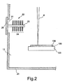
- Figure 2 shows a first possible way to introduce a getter member in the process chamber.
- the member is a true getter pump.
- the drawing shows in a broken view and schematically a part of the process chamber 13, defined by a wall 20.
- an opening 21 for connecting a getter pump 22 to the chamber is provided, the pump being e.g. comprised of a central support 23 on which a plurality of discs 24 made of a porous getter material are fixed.
- the support 23 is fixed to a flange 25 that closes opening 21 and also fixes the position of the pump.
- the getter pump may have also other structures, e.g. of the type shown in patents EP 650639 B1 , EP 650640 B1 or EP 910106 B1 .
- the pump is shown mounted on wall 20 and having the getter structure facing the inside of the chamber, but it is also possible to use an opposite arrangement, i.e. to arrange the getter pump is a small side chamber external to chamber 13 but communicating therewith through opening 21. In this second way it is also possible to provide for the use of a valve for closing aperture 21 and insulating the side chamber from the process chamber when needed, e.g. in order to change the getter pump or to carry out the reactivation treatment thereof.
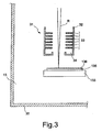
- Figure 3 shows a second possible way to introduce a getter member in the process chamber.
- the getter material is introduced into chamber 13 (defined by a wall 30) in the form of a pump 31.
- the pump has the shape of a hollow cylinder and is arranged coaxially to radiation R and proximate to the "X-Y" table 133.
- the pump 31 is comprised of a frame 32 (generally made of metal) and of a plurality of perforated discs 33 made of a porous getter material.
- the discs are shown simply fixed to frame 32, but it is obviously possible to resort to more elaborated solutions, in which the discs are fixed by means of metal members in order to form a self standing structure inserted in frame 32.
- the geometry of the getter material members could be different from the one shown and there could be used e.g. a geometry based on radially arranged planar getter members as disclosed in patent EP 650639 B1 , a sinusoidal getter member as disclosed in patent EP 918934 B1 or any other suitable geometry for this purpose.
- the lower portion of the frame is so shaped to form a volume 34 adapted to contain possible getter material particles that could detach from the above-standing getter members, in order to avoid that these particles fall onto table 133 or film 136.
- the hollow cylinder configuration is a preferred one, although any suitable hollow container may fulfill the same purpose and function.
- figure 4 shows a further possible way to introduce a getter member into the process chamber.
- the sorbing member is comprised of a deposit of getter material on a generally metal surface.
- Figure 4 shows a member 41 comprised of a getter material deposit 42 arranged on an inner wall of a hollow body 43, preferably cylindrical-shaped, that is coaxial to radiation R and arranged proximate to the "X-Y" table 133.
- deposit 42 is obtained by sputtering it is not necessary to resort to this solution, because the deposits obtained through this technique are generally compact and do not generate particulate.
- getter members and pumps work at room temperature.
- the surface of the getter material is used, the surface being thereby saturated after a certain number of hours of operation and being no longer able to carry out its task. It is thus possible to foresee the presence of heating elements for the getter member or pump (not shown in the drawings) for periodically reactivating the sorbing ability of the getter material, which reactivation may be carried out during the interruptions of the manufacturing process needed for servicing the apparatus.
- the getter elements of the getter pump may also be used to fix the getter elements of the getter pump, even though advantageous configurations envision the getter elements being disposed around the heating elements without being fixed thereto.
- a type of these getter pumps is sold by the applicant as CapaciTorr® D2000 MK5 getter pumps.
- Suitable getter materials for the invention may be comprised of one single metal chosen among titanium, zirconium, vanadium, niobium or hafnium or may have a composition formed of a number of metals.
- this is preferably titanium or zirconium.
- these are generally titanium- and/or zirconium-based alloys comprising at least another element chosen among transition elements, rare earths and aluminum, such as Zr-Fe, Zr-Ni, Zr-Al, Zr-V-Fe, Zr-Co-A alloys (where A indicates one or a number of elements chosen among yttrium, lanthanum and rare earths) or Zr-Ti-V alloys.
- this is preferably in a form having a high specific surface area (i.e. the surface area of the material for each gram of the same).
- This condition may be achieved by manufacturing highly porous getter material bodies, e.g. according to the techniques described in patent EP 719609 B1 or in patent application EP 1600232 A1 .
- getter material deposits formed on suitably shaped surfaces according to the technique described in patent application EP 1821328 A1 or by sputtering as described in patent EP 906635 B1 .
Landscapes
- Life Sciences & Earth Sciences (AREA)
- Atmospheric Sciences (AREA)
- Health & Medical Sciences (AREA)
- Epidemiology (AREA)
- Public Health (AREA)
- General Physics & Mathematics (AREA)
- Physics & Mathematics (AREA)
- Engineering & Computer Science (AREA)
- Environmental & Geological Engineering (AREA)
- Condensed Matter Physics & Semiconductors (AREA)
- Manufacturing & Machinery (AREA)
- Computer Hardware Design (AREA)
- Microelectronics & Electronic Packaging (AREA)
- Power Engineering (AREA)
- Exposure And Positioning Against Photoresist Photosensitive Materials (AREA)
- Exposure Of Semiconductors, Excluding Electron Or Ion Beam Exposure (AREA)
- Electron Tubes For Measurement (AREA)
Abstract
Description
- The present invention refers to a lithography apparatus using extreme UV radiation and having a Volatile Organic Compounds (VOCs) sorbing member comprising a getter material.
- Lithography is a technique used in the manufacturing of integrated circuits to define the geometry of the parts that form these circuits; the technique is also used in other similar manufacturing processes, such as those of micromechanical systems (known in the field as MEMs). In order to illustrate the invention, reference will be made in the text to the manufacturing of integrated circuits (known as ICs,), but the invention can be employed in all the manufacturing processes using the lithography technique.
- In the manufacturing of ICs, a film of a polymeric material, that shows the characteristic of being able to change its chemical behaviour (for example its solubility in a given solvent) upon the exposure to a radiation at a given wavelength, is positioned, or formed starting from liquid precursors, onto a slice of a supporting material, typically silicon or other semiconductor materials. By selectively illuminating with the suitable radiation only portions of the polymeric film, this is locally sensitized in such a way to make it subsequently attackable by a solvent (also the contrary is possible, i.e. that the film as such is attackable by the solvent and the radiation treatment makes it instead resistant thereto). After the selective illumination treatment, the portions rendered sensitive to the chemical attack of the solvent (or remained sensitive) are removed by a treatment with the latter, exposing only the desired portions of the supporting surface; on these portions it is then possible to form localized deposits of materials having desired characteristics, such as for example conducting or insulating materials, by techniques such as physical vapour deposition (PVD, a technique more commonly known in the field as "sputtering"), chemical vapour deposition (CVD), Molecular Beam Epitaxy (MBE) or the like; alternatively, the exposed portions of the supporting surface may undergo an erosive treatment in order to form recesses of suitable geometry in the surface of the support itself, for example by chemical attacks. By alternating subsequent cycles of positioning or depositing of the polymeric film, selectively removing of its portions and depositing "traces" of desired materials on the exposed portions of the support or erosion thereof, the desired structures of the integrated circuit are finally manufactured.
- In order to reduce the manufacturing costs and to follow the demand of the market for more and more compact electronic products, the typical dimensions of the parts that form integrated circuits undergo a constant reduction over time; at present the smallest dimension of IC parts that are obtained through lithographic techniques are about 100 nanometers (nm), but a transition to the next generation of ICs is already in progress, in which the smallest dimensions of IC parts will be around 30 nm.
- In order to be able to define smaller and smaller geometries and structures, during the lithographic operations it is necessary to use radiations of smaller wavelengths, comparable to the dimensions of these geometries. The main manufacturers of ICs have defined a new wavelength standard to be used for the manufacturing of ICs of the next generation, which is around 13.5 nm. This value is in the range of UV radiations of shorter wavelength, defined in the field as extreme UV (or EUV): Lithography that uses these radiations is consequently known in the field under the definition "Extreme UV Lithography", or under its abbreviation EUVL.
- The lithographic techniques employed up to now used wavelengths to which some gases, liquids or solids were transparent; it was thus possible, by suitably choosing the materials that formed the lithographic system, to obtain that the optical path of the UV radiation from the source to the polymeric film occurred in a gaseous medium (for example, purified air) and that the deviation and focusing of the radiation occurred essentially only by refraction through suitable lenses. By employing EUVL this is no longer possible, because the EUV wavelengths are almost completely sorbed by all materials. Consequently, in EUVL the optical path of the radiation can be defined only inside evacuated chambers and by using reflecting elements (mirrors, monochromators, ... ).
- EUVL apparatuses currently under development are comprised of various main chambers, connected to each other only through small openings for the passage of the radiation from one chamber to another. Normally, the EUV radiation source (in general a plasma generated by a laser or an electric discharge) and a collector, that collects a portion of the radiation emitted by the source and directs the radiation along a preferred direction, are arranged in a first chamber. In an intermediate chamber there is a part of the elements for focusing and directing the beam exiting from the first chamber (for example, a monochromator and system of reflecting elements to direct the radiation from the monochromator). Finally, in a last chamber, defined "process chamber" in the following, there are the final reflecting elements for focusing the radiation onto the support, preferably made of semiconductor material that holds the polymeric film to be treated by the radiation, and a sample holder on which said support is fixed, being able to move freely and in a controlled manner in a plane perpendicular to the incident direction of the radiation (sample holders known as "X-Y tables"). Pumping systems are connected to the apparatus in order to maintain the required vacuum degree inside it, generally comprising turbo-molecular or cryogenic pumps. The required vacuum degree is different in the various chambers, and is less severe in the first chamber, up to requiring values of residual pressure lower than 10-7 Pa in the process chamber. An example of an EUVL apparatus is disclosed in the patent application
US 2006/0175558 A1 , which is referred to for a more detailed explanation of the various parts of a similar apparatus and of their functions. - A problem with EUVL apparatuses is the presence of volatile organic molecules in the process chamber. These molecules, when irradiated by the highly energetic UV radiation, can mutually react or react with the surface of the support, preferably made of semiconductor material, thus resulting in new species or in carbon residuals, resistant to the subsequent chemical treatments, that may remain incorporated in the structures under formation and cause defects thereof, thus resulting in manufacturing waste. Decomposition of the organic molecules and deposition of carbon-based layers can also take place on the optical lenses present in the process chamber which have the task to reflect the radiation coming from the EUV source. The presence of carbon layers on the surface of the lenses reduces their optical reflectivity, thus decreasing the radiation intensity reaching the substrate. This in turn decreases the photolithographic efficiency and the overall process yield.
- Hydrocarbons are among the most common VOCs contaminants that may be present within the EUVL apparatuses.
- EUVL apparatuses are normally equipped with various pumping units in order to maintain the chambers under high vacuum, but the scanning of the radiation across the surface of the polymeric film on the support is a source of organic molecules, both coming from the decomposition of the polymer and from solvent molecules trapped therein. These molecules are thus formed and released in the most critical zone of the system.
- The pumping systems normally provided for maintaining the vacuum in EUVL apparatuses can not remove these species in a fast and effective way, before these can result in undesired reactions on or with the support, because these systems are normally positioned at far away from the support, which is also the zone wherein organic molecules are generated. In EUVL apparatuses it is not possible to bring the already present pumps closer to this zone, because the turbomolecular pumps would transmit vibrations to the reflecting elements or to the X-Y table, thus jeopardizing the scanning precision, whereas the cryogenic pumps would cause mechanical deformations in the system due to the high thermal gradients they generate, thus also resulting in this case in scanning imprecisions.
-
WO 2006/011105 discloses cleaning solutions and their arrangement for the EUV optics, by means of getter deposits placed in the vicinity of the optical elements, whileUS 2005/0122491 discloses the use of a contamination trap interposed between the UV light source, nearby the same, and the element to be exposed, with the UV light passing through the trap. Another approach to avoid optics contamination is disclosed inUS 2005/0229783 andUS 2007/0023709 , providing for the use of getter purifiers for the purge gas within the lithographic apparatus, rather than means to block the contamination coming from elements inside the EUV apparatus - Object of the present invention is thus to provide a lithography apparatus using extreme UV radiation capable of solving or anyway minimizing the problem of the presence of organic volatile molecules in the process chamber.
- According to the present invention, this object is obtained by means of a lithography apparatus according to claim 1.
- The inventors have found that getter materials, normally used in vacuum technology at operating temperatures of 200-300°C for sorbing simple gaseous species as H2, O2, H2O, CO and CO2, can effectively sorb VOCs, with particular and non-exclusive reference to hydrocarbons at room temperature. This makes the elements containing getter materials (these being bodies either formed of getter materials only or being deposits of these materials on surfaces, or real structured getter pumps) particularly suitable for the use proximate to the support in the process chamber of an EUVL system. As it is known in fact getter materials enable to manufacture gas sorbing members that have no moving parts and thus are free from vibrations, and the finding of the VOCs sorbing capacity at room temperature leads to the fact that these materials can be positioned very close to the support on which the polymeric film is arranged, i.e. the source of the volatile organic molecules, without altering the thermal balance of the system and thus without introducing scanning imprecisions of the UV radiation across the polymeric film.
- The invention will be illustrated in the following with reference to the annexed drawings, wherein:
-
figure 1 shows the general geometry of an EUVL apparatus; -
figure 2 shows a first possibility of positioning a getter member in the process chamber of an EUVL apparatus; -
figure 3 shows another possibility of positioning a getter member in the process chamber of an EUVL apparatus; and -
figure 4 shows a further possibility of positioning a getter member in the process chamber of an EUVL apparatus. - The dimensions of the elements and members shown in the drawings are not in scale, and in particular the thicknesses of some of those, such as the support, preferably made of semiconductor material, the polymeric film or the getter deposit shown in
figure 4 , have been largely increased to help to understand the drawings. - Moreover in the following reference will be made to the support as made of a semiconductor material, but this is only the preferred embodiment for carrying out the invention, and there may be cases in which devices may require a different type of material for the support, for example an insulating or non conducing material.
-
Figure 1 shows an EUVL apparatus in a schematic and extremely simplified way. Theapparatus 10 comprises afirst chamber 11, in which the EUVradiation source 110 and a collector 111 are present, the latter collecting parts of the radiation emitted from the source in all directions and directs the radiation to the subsequent chamber; asecond chamber 12, containing amonochromator 120 that selects the desired wavelength from the band of frequencies emitted from the source and directs the monochromatic radiation to the subsequent chamber; and aprocess chamber 13, containing asample holder 130 that holds amask 131 with the design to be reproduced on the polymeric film arranged on the support made of semiconductor material, at least one reflecting element 132 (but, in general a plurality of reflecting elements are provided, see for examplefigure 2 of patent applicationUS 2006/0175558 A1 ), and an "X-Y" table 133 moved by amotorized member 134. On table 133 asupport 135 made of a semiconductor material is arranged, on which apolymeric film 136 to be sensitized by the radiation is present; letter R infigure 1 indicates the path of the EUV radiation. - According to the invention, a getter member is arranged in the process chamber, in the area closest to the source of organic molecules.
-
Figure 2 shows a first possible way to introduce a getter member in the process chamber. In this case the member is a true getter pump. The drawing shows in a broken view and schematically a part of theprocess chamber 13, defined by awall 20. In the wall an opening 21 for connecting agetter pump 22 to the chamber is provided, the pump being e.g. comprised of acentral support 23 on which a plurality ofdiscs 24 made of a porous getter material are fixed. Thesupport 23 is fixed to aflange 25 that closes opening 21 and also fixes the position of the pump. The getter pump may have also other structures, e.g. of the type shown in patentsEP 650639 B1 EP 650640 B1 EP 910106 B1 figure 2 the pump is shown mounted onwall 20 and having the getter structure facing the inside of the chamber, but it is also possible to use an opposite arrangement, i.e. to arrange the getter pump is a small side chamber external tochamber 13 but communicating therewith through opening 21. In this second way it is also possible to provide for the use of a valve forclosing aperture 21 and insulating the side chamber from the process chamber when needed, e.g. in order to change the getter pump or to carry out the reactivation treatment thereof. -
Figure 3 shows a second possible way to introduce a getter member in the process chamber. Also in this case the getter material is introduced into chamber 13 (defined by a wall 30) in the form of apump 31. The pump has the shape of a hollow cylinder and is arranged coaxially to radiation R and proximate to the "X-Y" table 133. Thepump 31 is comprised of a frame 32 (generally made of metal) and of a plurality of perforated discs 33 made of a porous getter material. The discs are shown simply fixed toframe 32, but it is obviously possible to resort to more elaborated solutions, in which the discs are fixed by means of metal members in order to form a self standing structure inserted inframe 32. In addition the geometry of the getter material members could be different from the one shown and there could be used e.g. a geometry based on radially arranged planar getter members as disclosed in patentEP 650639 B1 EP 918934 B1 volume 34 adapted to contain possible getter material particles that could detach from the above-standing getter members, in order to avoid that these particles fall onto table 133 orfilm 136. - The hollow cylinder configuration is a preferred one, although any suitable hollow container may fulfill the same purpose and function.
- Finally,
figure 4 shows a further possible way to introduce a getter member into the process chamber. In this case the sorbing member is comprised of a deposit of getter material on a generally metal surface.Figure 4 shows amember 41 comprised of agetter material deposit 42 arranged on an inner wall of ahollow body 43, preferably cylindrical-shaped, that is coaxial to radiation R and arranged proximate to the "X-Y" table 133. Also in this case it is possible to provide for shaping the lower portion ofbody 43 in such a way to form a "drawer" (case not shown in the drawing) in order to retain particles possibly detached fromdeposit 42, in order to avoid that these particles fall onto table 133 orfilm 136. However, whendeposit 42 is obtained by sputtering it is not necessary to resort to this solution, because the deposits obtained through this technique are generally compact and do not generate particulate. - During the manufacturing steps carried out in the process chamber, getter members and pumps work at room temperature. However, in these conditions only the surface of the getter material is used, the surface being thereby saturated after a certain number of hours of operation and being no longer able to carry out its task. It is thus possible to foresee the presence of heating elements for the getter member or pump (not shown in the drawings) for periodically reactivating the sorbing ability of the getter material, which reactivation may be carried out during the interruptions of the manufacturing process needed for servicing the apparatus.
- When such a heating element is present, it may also be used to fix the getter elements of the getter pump, even though advantageous configurations envision the getter elements being disposed around the heating elements without being fixed thereto. A type of these getter pumps is sold by the applicant as CapaciTorr® D2000 MK5 getter pumps.
- Suitable getter materials for the invention may be comprised of one single metal chosen among titanium, zirconium, vanadium, niobium or hafnium or may have a composition formed of a number of metals. In the case of a single metal, this is preferably titanium or zirconium. In the case of multi-metal materials, these are generally titanium- and/or zirconium-based alloys comprising at least another element chosen among transition elements, rare earths and aluminum, such as Zr-Fe, Zr-Ni, Zr-Al, Zr-V-Fe, Zr-Co-A alloys (where A indicates one or a number of elements chosen among yttrium, lanthanum and rare earths) or Zr-Ti-V alloys.
- In order to increase the sorption speed (rate) of the getter material, this is preferably in a form having a high specific surface area (i.e. the surface area of the material for each gram of the same). This condition may be achieved by manufacturing highly porous getter material bodies, e.g. according to the techniques described in patent
EP 719609 B1 EP 1600232 A1 . Alternatively, it is possible to employ getter material deposits formed on suitably shaped surfaces, according to the technique described in patent applicationEP 1821328 A1 or by sputtering as described in patentEP 906635 B1 WO 2006/109343 A2 , i.e. under a pressure of noble gas (normally argon) in the sputtering chamber that is higher than the values normally used for the deposition of metal layers, and employing a power applied to the target that is lower than the values normally used in the technique.
Claims (13)
- A lithography apparatus (10) using extreme UV radiation having a vacuum process chamber (13) comprising a support (135) on which a polymeric film (136) to be sensitized by said radiation is present, characterized by having a Volatile Organic Compounds (VOCs) sorbing member (22; 31; 41) comprising a getter material arranged in the process chamber (13) or in a space connected thereto by means of an opening, characterised in that said sorbing member is proximate to the said support in the vacuum process chamber.
- An apparatus according to claim 1, wherein said VOCs sorbing member is a getter pump (22) comprising a getter pump support (23), said getter pump being inserted in the process chamber (13) through an opening (21) formed in a wall (20) thereof and connected to said wall by means of a flange (25) carrying said getter pump support (23).
- An apparatus according to claim 1, wherein said VOCs sorbing member is a getter pump arranged in a side chamber external to the process chamber and communicating therewith through said opening.
- An apparatus according to claim 1, wherein said VOCs sorbing member is a getter pump (22) comprised of a plurality of discs (24) made of a getter material and fixed to a central getter pump support (23).
- An apparatus according to claim 1, wherein said VOCs sorbing member is a getter pump (22) comprised of a plurality of discs (24) made of a getter material and an heating element, wherein said getter discs are fixed to said heating element.
- An apparatus according to claim 1, wherein said VOCs sorbing member is a getter pump comprised of a plurality of discs made of a getter material and a heating element, wherein said getter discs are disposed around said heating element without being fixed thereto.
- An apparatus according to claim 1, wherein said VOCs sorbing member is a getter pump (31) having the shape of a hollow container arranged in the process chamber coaxially to the UV radiation and proximate to the support on which the polymeric film to be sensitized by the radiation is present.
- An apparatus according to claim 7, wherein said hollow container is cylindrical-shaped.
- An apparatus according to claim 8, wherein said getter pump is comprised of a cylindrical frame (32) inside which a plurality of perforated discs (33) made of a getter material are present.
- An apparatus according to claim 8, wherein said getter pump is comprised of a cylindrical frame inside which a plurality of radially arranged planar members made of a getter material are present.
- An apparatus according to claim 1, wherein said VOCs sorbing member is a deposit of getter material on a metal surface.
- An apparatus according to claim 11, wherein said VOCs sorbing member (41) is comprised of a getter material deposit (42) on an inner wall of a hollow body (43) arranged coaxially to the UV radiation and proximate to the support on which the polymeric film to be sensitized by the radiation is present.
- An apparatus according to claim 1, wherein the getter material is chosen among titanium, zirconium, vanadium, niobium or hafnium, or alloys based on titanium and/or zirconium with at least another element chosen among transition elements, rare earths and aluminum.
Applications Claiming Priority (2)
| Application Number | Priority Date | Filing Date | Title |
|---|---|---|---|
| IT000282A ITMI20080282A1 (en) | 2008-02-22 | 2008-02-22 | LITHOGRAPHY APPARATUS WITH EXTREME UV RADIATION WITH AN ABSORBER ELEMENT OF HYDROCARBONS INCLUDING A GETTER MATERIAL |
| PCT/EP2009/051516 WO2009103631A1 (en) | 2008-02-22 | 2009-02-10 | Lithography apparatus using extreme uv radiation and having a volatile organic compounds sorbing member comprising a getter material |
Publications (2)
| Publication Number | Publication Date |
|---|---|
| EP2255252A1 EP2255252A1 (en) | 2010-12-01 |
| EP2255252B1 true EP2255252B1 (en) | 2011-06-29 |
Family
ID=40291682
Family Applications (1)
| Application Number | Title | Priority Date | Filing Date |
|---|---|---|---|
| EP09711636A Active EP2255252B1 (en) | 2008-02-22 | 2009-02-10 | Lithography apparatus using extreme uv radiation and having a volatile organic compounds sorbing member comprising a getter material |
Country Status (10)
| Country | Link |
|---|---|
| US (1) | US8399861B2 (en) |
| EP (1) | EP2255252B1 (en) |
| JP (2) | JP5411167B2 (en) |
| KR (1) | KR101429440B1 (en) |
| CN (2) | CN103345127B (en) |
| AT (1) | ATE514973T1 (en) |
| CA (1) | CA2711616A1 (en) |
| IT (1) | ITMI20080282A1 (en) |
| TW (1) | TW200951628A (en) |
| WO (1) | WO2009103631A1 (en) |
Families Citing this family (8)
| Publication number | Priority date | Publication date | Assignee | Title |
|---|---|---|---|---|
| JP5315100B2 (en) * | 2009-03-18 | 2013-10-16 | 株式会社ニューフレアテクノロジー | Drawing device |
| ITMI20121732A1 (en) | 2012-10-15 | 2014-04-16 | Getters Spa | GETTER PUMP |
| TWI660125B (en) * | 2014-04-03 | 2019-05-21 | 義大利商沙斯格特斯公司 | Getter pump |
| DE102016213830B3 (en) * | 2016-07-27 | 2017-12-07 | Carl Zeiss Smt Gmbh | Source hollow body and EUV plasma light source with such a hollow source body |
| KR20220076913A (en) | 2020-12-01 | 2022-06-08 | 포항공과대학교 산학협력단 | Nano lithography apparatus |
| CN113042160A (en) * | 2021-03-10 | 2021-06-29 | 南京华东电子真空材料有限公司 | Getter applied to extreme ultraviolet equipment and preparation device |
| DE102021205985A1 (en) * | 2021-06-11 | 2022-12-15 | Carl Zeiss Smt Gmbh | Optical arrangement for EUV lithography and method for regenerating a gas-binding component |
| DE102022102478A1 (en) * | 2022-02-02 | 2023-08-03 | Asml Netherlands B.V. | EUV lithography system with a gas-binding component |
Family Cites Families (21)
| Publication number | Priority date | Publication date | Assignee | Title |
|---|---|---|---|---|
| US4969556A (en) * | 1988-05-10 | 1990-11-13 | Hajime Ishimaru | Vacuum container |
| US5911560A (en) * | 1994-10-31 | 1999-06-15 | Saes Pure Gas, Inc. | Getter pump module and system |
| US5972183A (en) | 1994-10-31 | 1999-10-26 | Saes Getter S.P.A | Getter pump module and system |
| IT237018Y1 (en) * | 1995-07-10 | 2000-08-31 | Getters Spa | GETTER PUMP REFINED IN PARTICULAR FOR A PORTABLE CHEMICAL ANALYSIS INSTRUMENT |
| IT1295340B1 (en) * | 1997-10-15 | 1999-05-12 | Getters Spa | HIGH SPEED GAS ABSORPTION GETTER PUMP |
| US6391090B1 (en) * | 2001-04-02 | 2002-05-21 | Aeronex, Inc. | Method for purification of lens gases used in photolithography |
| JP2004053264A (en) | 2002-07-16 | 2004-02-19 | Konica Minolta Holdings Inc | Radiological image conversion panel and its manufacturing method |
| JP2004214480A (en) * | 2003-01-07 | 2004-07-29 | Nikon Corp | Aligner |
| KR101095394B1 (en) * | 2003-05-22 | 2011-12-16 | 코닌클리즈케 필립스 일렉트로닉스 엔.브이. | Method and device for cleaning at least one optical component |
| SG112047A1 (en) * | 2003-11-11 | 2005-06-29 | Asml Netherlands Bv | Lithographic apparatus with contamination suppression, device manufacturing method, and device manufactured thereby |
| JP2005244016A (en) * | 2004-02-27 | 2005-09-08 | Nikon Corp | Aligner, aligning method, and process for fabricating device having fine pattern |
| JP5122952B2 (en) * | 2004-07-22 | 2013-01-16 | コーニンクレッカ フィリップス エレクトロニクス エヌ ヴィ | Optical system having cleaning arrangement |
| US7868304B2 (en) * | 2005-02-07 | 2011-01-11 | Asml Netherlands B.V. | Method for removal of deposition on an optical element, lithographic apparatus, device manufacturing method, and device manufactured thereby |
| JP2006245254A (en) * | 2005-03-03 | 2006-09-14 | Nikon Corp | Exposure device, exposure method, and method for manufacturing device having fine pattern |
| JP2007018931A (en) * | 2005-07-08 | 2007-01-25 | Canon Inc | Light source device, exposure device, and manufacturing method of device |
| US7473908B2 (en) * | 2006-07-14 | 2009-01-06 | Asml Netherlands B.V. | Getter and cleaning arrangement for a lithographic apparatus and method for cleaning a surface |
| DE102006036488A1 (en) | 2006-08-04 | 2008-02-07 | Carl Zeiss Smt Ag | Optical system i.e. projection lens, for use in microlithography, has housing including two individual housing parts provided with optical unit, where flushing gas e.g. neon, flows via inlet opening into housing |
| US20080050680A1 (en) * | 2006-08-24 | 2008-02-28 | Stefan Brandl | Lithography systems and methods |
| US7959310B2 (en) * | 2006-09-13 | 2011-06-14 | Carl Zeiss Smt Gmbh | Optical arrangement and EUV lithography device with at least one heated optical element, operating methods, and methods for cleaning as well as for providing an optical element |
| DE102006044591A1 (en) | 2006-09-19 | 2008-04-03 | Carl Zeiss Smt Ag | Optical arrangement, in particular projection exposure apparatus for EUV lithography, as well as reflective optical element with reduced contamination |
| US7671348B2 (en) | 2007-06-26 | 2010-03-02 | Advanced Micro Devices, Inc. | Hydrocarbon getter for lithographic exposure tools |
-
2008
- 2008-02-22 IT IT000282A patent/ITMI20080282A1/en unknown
-
2009
- 2009-02-10 JP JP2010547146A patent/JP5411167B2/en active Active
- 2009-02-10 WO PCT/EP2009/051516 patent/WO2009103631A1/en active Application Filing
- 2009-02-10 KR KR1020107020658A patent/KR101429440B1/en active IP Right Grant
- 2009-02-10 CN CN201310276167.6A patent/CN103345127B/en active Active
- 2009-02-10 EP EP09711636A patent/EP2255252B1/en active Active
- 2009-02-10 CN CN200980103842.7A patent/CN101971098B/en active Active
- 2009-02-10 US US12/812,948 patent/US8399861B2/en active Active
- 2009-02-10 CA CA2711616A patent/CA2711616A1/en not_active Abandoned
- 2009-02-10 AT AT09711636T patent/ATE514973T1/en not_active IP Right Cessation
- 2009-02-16 TW TW098104833A patent/TW200951628A/en unknown
-
2013
- 2013-05-13 JP JP2013100962A patent/JP5357356B2/en active Active
Also Published As
| Publication number | Publication date |
|---|---|
| JP5411167B2 (en) | 2014-02-12 |
| KR20100119568A (en) | 2010-11-09 |
| JP2013165293A (en) | 2013-08-22 |
| CN103345127B (en) | 2016-01-20 |
| US8399861B2 (en) | 2013-03-19 |
| EP2255252A1 (en) | 2010-12-01 |
| JP5357356B2 (en) | 2013-12-04 |
| CN101971098A (en) | 2011-02-09 |
| US20100309446A1 (en) | 2010-12-09 |
| WO2009103631A1 (en) | 2009-08-27 |
| KR101429440B1 (en) | 2014-08-12 |
| CN101971098B (en) | 2013-07-10 |
| CN103345127A (en) | 2013-10-09 |
| ITMI20080282A1 (en) | 2009-08-23 |
| JP2011512684A (en) | 2011-04-21 |
| TW200951628A (en) | 2009-12-16 |
| ATE514973T1 (en) | 2011-07-15 |
| CA2711616A1 (en) | 2009-08-27 |
Similar Documents
| Publication | Publication Date | Title |
|---|---|---|
| EP2255252B1 (en) | Lithography apparatus using extreme uv radiation and having a volatile organic compounds sorbing member comprising a getter material | |
| US8598550B2 (en) | Ex-situ removal of deposition on an optical element | |
| US7355672B2 (en) | Method for the removal of deposition on an optical element, method for the protection of an optical element, device manufacturing method, apparatus including an optical element, and lithographic apparatus | |
| US7561247B2 (en) | Method for the removal of deposition on an optical element, method for the protection of an optical element, device manufacturing method, apparatus including an optical element, and lithographic apparatus | |
| EP2064005B1 (en) | Method and unit for cleaning a surface region covered with contaminant or undesirable material | |
| JP5381607B2 (en) | Extreme ultraviolet light equipment | |
| KR102615911B1 (en) | Vacuum actuator containment for mitigation of molecular contaminants and particles | |
| JP2009004647A (en) | Vacuum container, evaluation method and euv lithography | |
| JPH04233727A (en) | Selective coating method for thsin film |
Legal Events
| Date | Code | Title | Description |
|---|---|---|---|
| PUAI | Public reference made under article 153(3) epc to a published international application that has entered the european phase |
Free format text: ORIGINAL CODE: 0009012 |
|
| 17P | Request for examination filed |
Effective date: 20100909 |
|
| AK | Designated contracting states |
Kind code of ref document: A1 Designated state(s): AT BE BG CH CY CZ DE DK EE ES FI FR GB GR HR HU IE IS IT LI LT LU LV MC MK MT NL NO PL PT RO SE SI SK TR |
|
| AX | Request for extension of the european patent |
Extension state: AL BA RS |
|
| GRAP | Despatch of communication of intention to grant a patent |
Free format text: ORIGINAL CODE: EPIDOSNIGR1 |
|
| DAX | Request for extension of the european patent (deleted) | ||
| GRAS | Grant fee paid |
Free format text: ORIGINAL CODE: EPIDOSNIGR3 |
|
| GRAA | (expected) grant |
Free format text: ORIGINAL CODE: 0009210 |
|
| AK | Designated contracting states |
Kind code of ref document: B1 Designated state(s): AT BE BG CH CY CZ DE DK EE ES FI FR GB GR HR HU IE IS IT LI LT LU LV MC MK MT NL NO PL PT RO SE SI SK TR |
|
| REG | Reference to a national code |
Ref country code: GB Ref legal event code: FG4D |
|
| REG | Reference to a national code |
Ref country code: CH Ref legal event code: EP |
|
| REG | Reference to a national code |
Ref country code: IE Ref legal event code: FG4D |
|
| REG | Reference to a national code |
Ref country code: DE Ref legal event code: R096 Ref document number: 602009001695 Country of ref document: DE Effective date: 20110908 |
|
| REG | Reference to a national code |
Ref country code: NL Ref legal event code: VDEP Effective date: 20110629 |
|
| PG25 | Lapsed in a contracting state [announced via postgrant information from national office to epo] |
Ref country code: HR Free format text: LAPSE BECAUSE OF FAILURE TO SUBMIT A TRANSLATION OF THE DESCRIPTION OR TO PAY THE FEE WITHIN THE PRESCRIBED TIME-LIMIT Effective date: 20110629 Ref country code: NO Free format text: LAPSE BECAUSE OF FAILURE TO SUBMIT A TRANSLATION OF THE DESCRIPTION OR TO PAY THE FEE WITHIN THE PRESCRIBED TIME-LIMIT Effective date: 20110929 Ref country code: SE Free format text: LAPSE BECAUSE OF FAILURE TO SUBMIT A TRANSLATION OF THE DESCRIPTION OR TO PAY THE FEE WITHIN THE PRESCRIBED TIME-LIMIT Effective date: 20110629 Ref country code: LT Free format text: LAPSE BECAUSE OF FAILURE TO SUBMIT A TRANSLATION OF THE DESCRIPTION OR TO PAY THE FEE WITHIN THE PRESCRIBED TIME-LIMIT Effective date: 20110629 |
|
| PG25 | Lapsed in a contracting state [announced via postgrant information from national office to epo] |
Ref country code: FI Free format text: LAPSE BECAUSE OF FAILURE TO SUBMIT A TRANSLATION OF THE DESCRIPTION OR TO PAY THE FEE WITHIN THE PRESCRIBED TIME-LIMIT Effective date: 20110629 Ref country code: LV Free format text: LAPSE BECAUSE OF FAILURE TO SUBMIT A TRANSLATION OF THE DESCRIPTION OR TO PAY THE FEE WITHIN THE PRESCRIBED TIME-LIMIT Effective date: 20110629 Ref country code: SI Free format text: LAPSE BECAUSE OF FAILURE TO SUBMIT A TRANSLATION OF THE DESCRIPTION OR TO PAY THE FEE WITHIN THE PRESCRIBED TIME-LIMIT Effective date: 20110629 Ref country code: GR Free format text: LAPSE BECAUSE OF FAILURE TO SUBMIT A TRANSLATION OF THE DESCRIPTION OR TO PAY THE FEE WITHIN THE PRESCRIBED TIME-LIMIT Effective date: 20110930 Ref country code: AT Free format text: LAPSE BECAUSE OF FAILURE TO SUBMIT A TRANSLATION OF THE DESCRIPTION OR TO PAY THE FEE WITHIN THE PRESCRIBED TIME-LIMIT Effective date: 20110629 |
|
| PG25 | Lapsed in a contracting state [announced via postgrant information from national office to epo] |
Ref country code: BE Free format text: LAPSE BECAUSE OF FAILURE TO SUBMIT A TRANSLATION OF THE DESCRIPTION OR TO PAY THE FEE WITHIN THE PRESCRIBED TIME-LIMIT Effective date: 20110629 |
|
| PG25 | Lapsed in a contracting state [announced via postgrant information from national office to epo] |
Ref country code: NL Free format text: LAPSE BECAUSE OF FAILURE TO SUBMIT A TRANSLATION OF THE DESCRIPTION OR TO PAY THE FEE WITHIN THE PRESCRIBED TIME-LIMIT Effective date: 20110629 Ref country code: EE Free format text: LAPSE BECAUSE OF FAILURE TO SUBMIT A TRANSLATION OF THE DESCRIPTION OR TO PAY THE FEE WITHIN THE PRESCRIBED TIME-LIMIT Effective date: 20110629 Ref country code: IS Free format text: LAPSE BECAUSE OF FAILURE TO SUBMIT A TRANSLATION OF THE DESCRIPTION OR TO PAY THE FEE WITHIN THE PRESCRIBED TIME-LIMIT Effective date: 20111029 Ref country code: PT Free format text: LAPSE BECAUSE OF FAILURE TO SUBMIT A TRANSLATION OF THE DESCRIPTION OR TO PAY THE FEE WITHIN THE PRESCRIBED TIME-LIMIT Effective date: 20111031 Ref country code: CZ Free format text: LAPSE BECAUSE OF FAILURE TO SUBMIT A TRANSLATION OF THE DESCRIPTION OR TO PAY THE FEE WITHIN THE PRESCRIBED TIME-LIMIT Effective date: 20110629 |
|
| PG25 | Lapsed in a contracting state [announced via postgrant information from national office to epo] |
Ref country code: PL Free format text: LAPSE BECAUSE OF FAILURE TO SUBMIT A TRANSLATION OF THE DESCRIPTION OR TO PAY THE FEE WITHIN THE PRESCRIBED TIME-LIMIT Effective date: 20110629 Ref country code: CY Free format text: LAPSE BECAUSE OF FAILURE TO SUBMIT A TRANSLATION OF THE DESCRIPTION OR TO PAY THE FEE WITHIN THE PRESCRIBED TIME-LIMIT Effective date: 20110629 Ref country code: SK Free format text: LAPSE BECAUSE OF FAILURE TO SUBMIT A TRANSLATION OF THE DESCRIPTION OR TO PAY THE FEE WITHIN THE PRESCRIBED TIME-LIMIT Effective date: 20110629 |
|
| PLBE | No opposition filed within time limit |
Free format text: ORIGINAL CODE: 0009261 |
|
| STAA | Information on the status of an ep patent application or granted ep patent |
Free format text: STATUS: NO OPPOSITION FILED WITHIN TIME LIMIT |
|
| 26N | No opposition filed |
Effective date: 20120330 |
|
| PG25 | Lapsed in a contracting state [announced via postgrant information from national office to epo] |
Ref country code: DK Free format text: LAPSE BECAUSE OF FAILURE TO SUBMIT A TRANSLATION OF THE DESCRIPTION OR TO PAY THE FEE WITHIN THE PRESCRIBED TIME-LIMIT Effective date: 20110629 |
|
| REG | Reference to a national code |
Ref country code: DE Ref legal event code: R097 Ref document number: 602009001695 Country of ref document: DE Effective date: 20120330 |
|
| PG25 | Lapsed in a contracting state [announced via postgrant information from national office to epo] |
Ref country code: MC Free format text: LAPSE BECAUSE OF NON-PAYMENT OF DUE FEES Effective date: 20120229 |
|
| REG | Reference to a national code |
Ref country code: IE Ref legal event code: MM4A |
|
| PG25 | Lapsed in a contracting state [announced via postgrant information from national office to epo] |
Ref country code: IE Free format text: LAPSE BECAUSE OF NON-PAYMENT OF DUE FEES Effective date: 20120210 |
|
| PG25 | Lapsed in a contracting state [announced via postgrant information from national office to epo] |
Ref country code: MK Free format text: LAPSE BECAUSE OF FAILURE TO SUBMIT A TRANSLATION OF THE DESCRIPTION OR TO PAY THE FEE WITHIN THE PRESCRIBED TIME-LIMIT Effective date: 20110629 |
|
| PG25 | Lapsed in a contracting state [announced via postgrant information from national office to epo] |
Ref country code: ES Free format text: LAPSE BECAUSE OF FAILURE TO SUBMIT A TRANSLATION OF THE DESCRIPTION OR TO PAY THE FEE WITHIN THE PRESCRIBED TIME-LIMIT Effective date: 20111010 |
|
| PG25 | Lapsed in a contracting state [announced via postgrant information from national office to epo] |
Ref country code: BG Free format text: LAPSE BECAUSE OF FAILURE TO SUBMIT A TRANSLATION OF THE DESCRIPTION OR TO PAY THE FEE WITHIN THE PRESCRIBED TIME-LIMIT Effective date: 20110929 |
|
| PG25 | Lapsed in a contracting state [announced via postgrant information from national office to epo] |
Ref country code: MT Free format text: LAPSE BECAUSE OF FAILURE TO SUBMIT A TRANSLATION OF THE DESCRIPTION OR TO PAY THE FEE WITHIN THE PRESCRIBED TIME-LIMIT Effective date: 20110629 |
|
| REG | Reference to a national code |
Ref country code: CH Ref legal event code: PL |
|
| PG25 | Lapsed in a contracting state [announced via postgrant information from national office to epo] |
Ref country code: CH Free format text: LAPSE BECAUSE OF NON-PAYMENT OF DUE FEES Effective date: 20130228 Ref country code: LI Free format text: LAPSE BECAUSE OF NON-PAYMENT OF DUE FEES Effective date: 20130228 |
|
| PG25 | Lapsed in a contracting state [announced via postgrant information from national office to epo] |
Ref country code: TR Free format text: LAPSE BECAUSE OF FAILURE TO SUBMIT A TRANSLATION OF THE DESCRIPTION OR TO PAY THE FEE WITHIN THE PRESCRIBED TIME-LIMIT Effective date: 20110629 |
|
| PG25 | Lapsed in a contracting state [announced via postgrant information from national office to epo] |
Ref country code: LU Free format text: LAPSE BECAUSE OF NON-PAYMENT OF DUE FEES Effective date: 20120210 |
|
| PG25 | Lapsed in a contracting state [announced via postgrant information from national office to epo] |
Ref country code: HU Free format text: LAPSE BECAUSE OF FAILURE TO SUBMIT A TRANSLATION OF THE DESCRIPTION OR TO PAY THE FEE WITHIN THE PRESCRIBED TIME-LIMIT Effective date: 20090210 |
|
| REG | Reference to a national code |
Ref country code: FR Ref legal event code: PLFP Year of fee payment: 8 |
|
| REG | Reference to a national code |
Ref country code: FR Ref legal event code: PLFP Year of fee payment: 9 |
|
| REG | Reference to a national code |
Ref country code: FR Ref legal event code: PLFP Year of fee payment: 10 |
|
| PGFP | Annual fee paid to national office [announced via postgrant information from national office to epo] |
Ref country code: FR Payment date: 20230223 Year of fee payment: 15 |
|
| PGFP | Annual fee paid to national office [announced via postgrant information from national office to epo] |
Ref country code: IT Payment date: 20230221 Year of fee payment: 15 |
|
| P01 | Opt-out of the competence of the unified patent court (upc) registered |
Effective date: 20230515 |
|
| PGFP | Annual fee paid to national office [announced via postgrant information from national office to epo] |
Ref country code: DE Payment date: 20240228 Year of fee payment: 16 Ref country code: GB Payment date: 20240227 Year of fee payment: 16 |