EP2251680B2 - X-ray inspection device - Google Patents
X-ray inspection device Download PDFInfo
- Publication number
- EP2251680B2 EP2251680B2 EP10162321.3A EP10162321A EP2251680B2 EP 2251680 B2 EP2251680 B2 EP 2251680B2 EP 10162321 A EP10162321 A EP 10162321A EP 2251680 B2 EP2251680 B2 EP 2251680B2
- Authority
- EP
- European Patent Office
- Prior art keywords
- slit
- width
- scintillator
- rays
- inspection device
- Prior art date
- Legal status (The legal status is an assumption and is not a legal conclusion. Google has not performed a legal analysis and makes no representation as to the accuracy of the status listed.)
- Active
Links
Images


Classifications
-
- G—PHYSICS
- G01—MEASURING; TESTING
- G01N—INVESTIGATING OR ANALYSING MATERIALS BY DETERMINING THEIR CHEMICAL OR PHYSICAL PROPERTIES
- G01N23/00—Investigating or analysing materials by the use of wave or particle radiation, e.g. X-rays or neutrons, not covered by groups G01N3/00 – G01N17/00, G01N21/00 or G01N22/00
- G01N23/02—Investigating or analysing materials by the use of wave or particle radiation, e.g. X-rays or neutrons, not covered by groups G01N3/00 – G01N17/00, G01N21/00 or G01N22/00 by transmitting the radiation through the material
- G01N23/06—Investigating or analysing materials by the use of wave or particle radiation, e.g. X-rays or neutrons, not covered by groups G01N3/00 – G01N17/00, G01N21/00 or G01N22/00 by transmitting the radiation through the material and measuring the absorption
- G01N23/083—Investigating or analysing materials by the use of wave or particle radiation, e.g. X-rays or neutrons, not covered by groups G01N3/00 – G01N17/00, G01N21/00 or G01N22/00 by transmitting the radiation through the material and measuring the absorption the radiation being X-rays
Definitions
- the present invention relates to an X-ray inspection device for irradiating articles with X-rays and detecting foreign matter in the articles.
- X-ray inspection devices or similar devices are conventionally used to detect foreign matter in articles. Research and development efforts are currently being conducted in relation to such devices.
- JP '066 publication there is disclosed a component of a radiation detector for minimizing the space required for wire bonding; making the radiation detector smaller in size and simpler to manufacture; and facilitating the manufacture of a two-dimensional detector.
- the component for a radiation detector is a component used in an X-ray inspection device.
- the component of a radiation detector according to JP '066 publication includes a photoelectric element arranged on a portion of an upper surface of a substrate to output an electrical signal based on the intensity of light received by the photoelectric element.
- the photoelectric element has a first pad provided on its light-receiving surface.
- the component of a radiation detector has a pad-formation portion arranged on a portion of the substrate other than a portion where the photoelectric element is arranged, and a second pad formed on the pad formation section.
- the second pad is arranged to form the same plane as that of the first pad arranged on the light-receiving surface of the photoelectric element, and is electrically connected to the first pad.
- JP '066 publication there is also disclosed a component of a radiation detector that further includes an optical waveguide path provided upstream in the light-receiving direction of a light receiving surface of a photoelectric element (see Claim 22 and FIG. 7 of JP '066 publication).
- US2006/0289765A1 discloses an X-ray inspection device adapted to detect foreign matter in a target object while the target object is conveyed, the X-ray inspection device comprising an X-ray emission device configured and arranged to emit X-rays at the target object; a scintillator unit configured and arranged to optically convert the X-rays emitted by the X-ray emission device into visible light, the scintillator unit extending in a direction that intersects a conveyance direction of the target object; and a photodiode array configured and arranged to detect the visible light optically converted by the scintillator unit and to convert the visible light into an electrical signal, the photodiode array being disposed along a direction in which the scintillator unit extends,
- WO99/63364 discloses an imaging detector having a collimator including chambers with an end defining an exit aperture cross section, a scintillator including segments with a first end defining a first aperture cross section matching one of the exit aperture cross sections and with a second end defining a second aperture cross section, and a photo detector array having elements having a cross section matching one of the second aperture cross section.
- EP 0 166 567A2 discloses an imaging system having an x-ray source for directing a beam of x-ray energy through the patient and onto a multi-element detector assembly.
- the detector elements of the detector assembly produce analog electrical signals during scanning the patient body.
- US patent 4,870,279 discloses an imaging X-ray sensor having a linear array of microscopically small bars of polycrystalline ceramic scintillator material bonded at the bar ends to an integrated circuit photodetector array.
- US patent 5,132,995 discloses an X-ray analysis apparatus having an x-ray source, a detector array and a collimator slit.
- the x-ray radiation from the source passes through the slit in the collimator and passes through a patient body.
- US 4366382A discloses a baggage system which employs a fan-shaped x-ray beam which scans baggage on a conveyor belt and produces images of the contents of the baggage on a video monitor.
- the scintillator array must be made several millimeters wide, even if the width of the PDA is extremely small; i.e., about 0.1 to 0.9 mm.
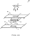
- FIG. 10 is a schematic cross-sectional view for describing a state in a conventional X-ray inspection device 900 that results in the detection of fine foreign matter being hindered.
- X-rays S1 are emitted from an X-ray emission device 200 and penetrate a conveyor belt 801, and visible light is emitted from scintillator elements 310a, 310b, 310c, 310d, and 310e of a scintillator 300.
- the visible light is received by a PDA 400, and an electrical signal is generated.
- the scintillator elements 310a, 310b, 310c, 310d, and 310e of the scintillator 300 emit visible light over 360 degrees in all directions.
- An object of the present invention is to provide an X-ray inspection device capable of reliably detecting fine foreign matter using a simple mechanism.
- An X-ray inspection device is defined by the appended claim 1.
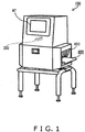
- FIG. 1 is a schematic external view showing an X-ray inspection device 100 according to the present invention
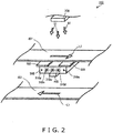
- FIG. 2 is a schematic diagram showing an interior of the X-ray inspection device 100 according to the present invention.
- an X-ray emission device 200 is installed in the X-ray inspection device 100.
- a product to be examined is placed on a conveyor belt 800 and transported through the X-ray inspection device 100, during which time an X-ray inspection is performed therein to examine whether the products contain foreign matter.
- the conveyor belt 800 of the X-ray inspection device 100 is formed so as to protrude outwards from the X-ray inspection device 100, and a plurality of X-ray shielding curtains 850 are provided.
- An operator operates a touch panel MT to drive the X-ray inspection device 100.
- An internal structure of the X-ray inspection device 100 will now be described.
- the X-ray inspection device 100 includes the X-ray emission device 200, the conveyor belt 800, a slit member 500, an irradiation width adjustment mechanism 510 (see FIG. 3 ), a scintillator 300 (a scintillator unit), and a photodiode array ("PDA" hereafter) 400.
- the conveyor belt 800 includes an endless belt rolled around a pair of rollers. In FIG. 2 , a portion of the belt travelling along a forward route is shown as a conveyor belt 801, and a portion of the belt travelling along a return route is shown as a conveyor belt 802.
- the slit member 500, the scintillator 300, and the PDA 400 are positioned in the stated sequence listed from the top; and are provided between the conveyor belt 801 and the conveyor belt 802, and the X-ray emission device 200 is provided above the conveyor belt 801.
- the conveyor belt 801 conveys an article in the conveyance direction indicated by the arrow L1.
- the conveyor belt 802 travels in the direction indicated by the arrow -L1, and thereby returns to the forward route side of the conveyor belt 801.
- damping of X-rays S1 is only affected by the conveyor belt 801 of the conveyor belts 801 and 802, and is not influenced by the conveyor belt 802.
- X-rays S1 are emitted from the X-ray emission device 200 in FIG. 2 .
- the conveyor belt 801 located above the slit member 500, the scintillator 300, and the PDA 400, conveys an article 600 in the conveyance direction indicated by the arrow L1.
- the scintillator 300 has scintillator elements 310a, 310b, 310c, 310d, and 310e.
- scintillator elements 310a through 310e there are five scintillator elements 310a through 310e; however, in reality, the scintillator 300 has numerous scintillator elements.
- a slit formed by the slit member 500 in FIG. 2 extends in a direction perpendicular to the conveyance direction indicated by the arrow L1.
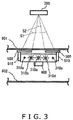
- FIG. 3 is a schematic diagram showing a side view of the X-ray inspection device 100 in FIG. 2
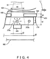
- FIGS. 4 and 5 are enlarged schematic diagrams showing a part of FIG. 3 .
- the scintillator element 310d is omitted in FIGS. 4 and 5 .
- the scintillator 300 is affixed to the PDA 400 using a chemical adhesive.
- the X-ray emission device 200 emits the X-rays S1.
- the presence of the slit member 500 results in the scintillator 300 being irradiated only with X-rays within the range shown by X-rays S2, and the remaining X-rays S1 are reflected by the slit member 500.
- X-rays S2 are part of X-rays S1 within the range corresponding to the slit of the slit member 500.
- the slit and the X-rays S2 depend on the width at which the PDA 400 receives the visible light converted by the scintillator 300.
- the layer of the slit member 500 is not provided, and the scintillator 300 is therefore irradiated with X-rays within the range shown by X-rays S1.
- optical conversion into visible light also occurs even in the scintillator elements 310a, 310e of the scintillator 300, and the PDA 400 receives the visible light from all of the scintillator elements 310a through 310e.
- the outline of fine foreign matter in the article thereby becomes blurred even when fine foreign matter is present in the article, and detection of the fine foreign matter becomes difficult.
- a specific example of a state in which detection of fine foreign matter becomes difficult as described above will be given further below.
- H1 is the width of the PDA 400 as measured in the conveyance direction (L1)
- A2 and H2 are respectively the thickness of the scintillator 300 as measured in a vertical direction and the width of the scintillator 300 as measured in the conveyance direction (L1)
- A3 is the thickness of the slit member 500 as measured in the vertical direction
- H3 is the slit width as measured in the conveyance direction (L1)
- the irradiation width adjustment mechanism 510 is used to move the slit member 500 in the vertical direction (indicated by the arrow M510) to change the spacing between the scintillator 300 and the slit member 500 from a distance A23 to a distance A23a.
- the irradiation width of the X-rays S2 can thereby be changed to an irradiation width of X-rays S21.
- the irradiation width adjustment mechanism 510 can be used to adjust the width of irradiation of the X-rays S2 reaching the scintillator 300.
- the vertical spacing between the scintillator 300 and the slit member 500 can be adjusted, whereby the irradiation width and the amount of X-rays S2 incident on the scintillator 300 can be adjusted.
- Affixing the scintillator 300 to the PDA 400 using the chemical adhesive and providing the slit member 500, as described above, eliminates the need to manufacture the scintillator 300 so that the width H2 of the scintillator 300 matches the width H1 of the PDA 400. In other words, it is possible to ameliorate decreases in yield due to such problems as faulty adhesion between the scintillator 300 and the PDA 400 in cases where the scintillator 300 is manufactured to match the width H1 of the PDA 400. Also, it becomes possible to reduce the cost necessary to manufacture a small scintillator 300 that matches the width H1 of the PDA 400.
- FIG. 6 is a graph showing examples of MTF curves
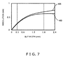
- FIG. 7 is a graph showing examples of resolution depending on slit width
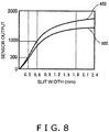
- FIG. 8 is a graph showing examples of sensor output depending on slit width
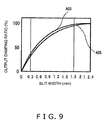
- FIG. 9 is a graph showing examples of output damping ratio depending on slit width.
- the MTF curves shown in FIG. 6 represent spatial frequency, which is the number of cycles per unit length (millimeter) in the horizontal axis, and the contrast reproduction capability (MTF: Modulation Transfer Function) normalized to 1 or 100 at zero frequency in the vertical axis.
- the spatial frequency is a value that represents the spacing between each stripe in a regularly repeating black-and-white stripe pattern.
- the experiment relating to FIG. 6 was performed under a condition in which the thickness A2 of the scintillator 300 was 0.3 mm.
- a higher spatial frequency can be maintained when there is a slit member forming a slit as compared to when there is no slit member. And thus, it is preferable to provide a slit member to the X-ray inspection device.
- the horizontal axis in FIG. 7 represents slit width H3 (mm), and the vertical axis represents resolution (mm).
- the inverse of the value of the spatial frequency at the point where the MTF value first falls below 0.1 was defined as the resolution (mm).
- curve A03 represents an instance where the thickness A2 of the scintillator 300 is 0.3 mm
- curve A05 represents an instance where the thickness A2 of the scintillator 300 is 0.5 mm.
- Each of curves A03 and A05 is a polynomial approximation curve, estimated from points corresponding to the slit width H3 being changed to 0.6 mm, 0.9 mm, 1.2 mm, 1.5 mm, 1.8 mm, and 2.4 mm, respectively.
- the curve A03 has a higher resolution in all regions compared to the curve A05; as a result, it can be seen that the resolution is higher in the present experiment when the thickness A2 of the scintillator 300 is 0.3 mm than when the thickness A2 is 0.5 mm.
- results shown in FIG. 7 show that the resolution becomes constant on the curve A03 at a slit width H3 of over 1.8 mm.
- the upper limit of the slit width H3 is 1.8 mm; increasing the slit width H3 to over 1.8 mm offers no benefit.
- the horizontal axis represents slit width (mm), and the vertical axis represents sensor output.
- the sensor output represents the value of the electrical signal output from the PDA 400.
- curve A03 represents an instance where the thickness A2 of the scintillator 300 is 0.3 mm
- curve A05 represents an instance where the thickness A2 of the scintillator 300 is 0.5 mm.
- Each of curves A03 and A05 is a polynomial approximation curve, estimated from points corresponding to the slit width H3 being changed to 0.6 mm, 0.9 mm, 1.2 mm, 1.5 mm, 1.8 mm, and 2.4 mm, respectively.
- the curve A03 has a higher sensor output value than the curve A05, showing that optical conversion is more efficient when the thickness A2 of the scintillator 300 is 0.3 mm than when the thickness A2 is 0.5 mm.
- FIG. 8 shows that the sensor output becomes constant at a slit width H3 of over 1.8 mm.
- the upper limit of the slit width H3 is 1.8 mm; increasing the slit width H3 to over 1.8 mm offers no benefit.
- the lower limit of the slit width H3 is 0.3 mm.
- the noise When the signal-to-noise ratio in the sensor output is taken into consideration, it is preferable for the noise to have a constant value and the signal to be larger. In order to perform image processing more properly, it is preferable for the sensor output to be about 1000 or higher. Therefore, when the thickness A2 of the scintillator 300 is 0.3 mm, the lower limit of the slit width H3 is preferably approximately 0.6 mm.
- the slit width H3 is preferably between 0.3 mm and 1.8 mm.
- the upper limit of the slit width H3 is 1.8 mm, and the ratio between the thickness A2 of the scintillator 300 and the upper limit of the slit width H3 is therefore 1:6.
- the lower limit of the slit width H3 is 0.3 mm, and the ratio between the thickness A2 of the scintillator 300 and the lower limit of the slit width H3 is therefore 1:1.
- the ratio between the thickness A2 of the scintillator 300 and the slit width H3 is preferably between 1:6 and 1:1. In such an instance, the X-rays that had passed through the slit can be optically converted in the scintillator 300 with a high degree of efficiency.
- the width H1 of the PDA 400 is 0.6 mm
- the upper limit of the slit width H3 is 1.8 mm
- the ratio between the width H1 of the PDA 400 and the upper limit of the slit width H3 is therefore 1:3.
- the lower limit value of the sensor output is approximately 300 and the lower limit of the slit width H3 is 0.3 mm, and the ratio between the width H1 of the PDA 400 and the lower limit of the slit width H3 is therefore 2:1.
- the sensor output is preferably about 1000 or higher; therefore, the lower limit of the slit width H3 is 0.6 mm. Also, since the width H1 of the PDA 400 is 0.6 mm, the ratio between the width H1 of the PDA 400 and the lower limit of the slit width H3 is 1:1.
- the ratio between the width H1 of the PDA 400 and the slit width H3 is preferably between 2:1 1 and 1:3, and more preferably between 1:1 and 1:3.
- the slit width H3 is narrower than the scintillator unit width H2 and equal to or wider than half a width of the light-receiving width H1 of the photodiode array 400. Therefore, a high level of resolution and electrical signal in the photodiode array 400 can be maintained.
- the horizontal axis represents slit width (mm), and the vertical axis represents the output damping ratio (%).
- the curve A03 represents an instance where the thickness A2 of the scintillator 300 is 0.3 mm
- the curve A05 represents an instance where the thickness A2 of the scintillator 300 is 0.5 mm.
- Each of curves A03 and A05 is a polynomial approximation curve, estimated from points corresponding to the slit width H3 being changed to 0.6 mm, 0.9 mm, 1.2 mm, 1.5 mm, 1.8 mm, and 2.4 mm, respectively.
- the curve A03 displays a greater output damping ratio than the curve A05, and a higher output damping ratio (%) is maintained in an instance where the thickness A2 of the scintillator 300 is 0.3 mm in comparison to when the thickness A2 is 0.5 mm.
- the thickness A2 of the scintillator 300 is preferably 0.3 mm
- the slit width H3 of the slit formed by the slit member 500 is preferably within the range of between 0.6 mm and 1.8 mm.
- FIGS. 10 and 11 are schematic views for describing the conventional X-ray inspection device 900
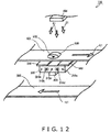
- FIGS. 12 and 13 are schematic views for describing the X-ray inspection device 100 according to the present invention.
- X-rays S1 are emitted by the X-ray emission device 200, and the article 600 having fine foreign matter 610 is conveyed in the conveyance direction indicated by the arrow L1.
- the X-rays S1 hardly penetrate the fine foreign matter 610 in the article 600. Therefore, the X-rays S1 are hardly incident on the scintillator element 310c of the scintillator 300, and it is only the scintillator element 310c where the X-rays are hardly converted into visible light.
- the scintillator elements 310a, 310b, 310d, and 310e emit visible light in all directions; therefore, visible light KSD (i.e., diffracted light) travelling in a diagonal direction reaches the PDA 400 as shown in FIG. 11 . Accordingly, in an instance where the fine foreign matter 610 in the article 600 is extremely small, there may be an instance where no difference appears in the electrical output signal outputted by the PDA 400, and the presence of the fine foreign matter 610 in the article 600 is not identified. In other words, the visible light KSD substantially cancels out a variation caused by the fine foreign matter 610.
- the visible light KSD is an integrated light of visible light emitted by the scintillator elements 310a and 310b and travelling in a downward direction at about 45 degrees angle, and visible light emitted by the scintillator elements 310d and 310e and travelling in a downward direction at about 45 degrees angle.
- the X-rays S1 are emitted by the X-ray emission device 200; however, the presence of the slit member 500 causes the scintillator 300 to be irradiated with X-rays S2 having a narrower width than the X-rays S1.
- the article 600 is then conveyed in the conveyance direction indicated by the arrow L1.
- the fine foreign matter 610 in the article 600 and the slit member 500 hardly allow the X-rays S1 to penetrate therethrough. Therefore, the scintillator elements 310a, 310c, and 310e of the scintillator 300 are hardly irradiated with the X-rays S1 and X-rays S2. As a result, the effect of diffracted visible light from the sides of scintillator elements 310a and 310e towards the side of the scintillator element 310c can be significantly reduced.
- the PDA 400 is hardly exposed to the diagonally travelling visible light KSD as shown in FIG. 11 , and is exposed to visible light KSE travelling downwards in a substantially vertical direction as shown in FIG. 13 .
- the scintillator elements 310a and 310e hardly perform optical conversion;
- the visible light KSE is an integrated light of visible light travelling almost directly downwards and visible light travelling in a downward direction at about 45 degrees angle emitted by the scintillator element 310b, and visible light travelling almost directly downwards and visible light travelling in a downward direction at about 45 degrees angle emitted by the scintillator element 310d.
- the fine foreign matter 610 in the article 600 is extremely small, a difference appears in visible light reaching the PDA 400, making it possible to reliably detect the fine foreign matter 610 in the article 600.
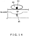
- FIG. 14 is a drawing for describing an effect of the present invention.
- the vertical axis represents the electrical signal outputted by the PDA 400, and the horizontal axis represents time.
- the X-ray inspection device 100 in an instance where the X-ray inspection device 100 according to the present invention is used, light can be prevented from diffracting, and the visible light KSE causes the fine foreign matter 610 in the article 600 to be visible within region AR1.
- the region AR1 is several times greater than the region AR9; therefore, the fine foreign matter 610 can be reliably detected.
- the presence of the slit member 500 causes the X-rays S1 to reach only the minimum necessary area of the scintillator 300 for the PDA 400 ultimately to receive the visible light.
- the presence of the slit member 500 prevents the X-rays S1 from reaching the portion of the scintillator 300 located in the vicinity below the fine foreign matter, and therefore diffracting of the visible light can be prevented.
- the width H3 of the slit defined by the slit member 500 is smaller than the width H2 of the scintillator 300, and larger than the width H1 of the photodiode array 400.
- the cost of manufacturing the X-ray inspection device 100 can be reduced.
- the slit of the slit member 500 is provided in a direction that intersects the conveyance direction of the article indicated by the arrow L1
- a shadow of the fine foreign matter 610 in the article 600 that passes above the slit member 500 can be made sharper.
- the X-rays reach the scintillator 300 through the slit member 500 without loss of intensity. As a result, it is possible to adjust the intensity of the X-rays as appropriate and perform X-ray inspection in an efficient manner.
- the article 600 corresponds to a target object
- the X-rays S1, S2 correspond to X-rays
- the X-ray emission device 200 corresponds to an X-ray emission device
- the scintillator 300 corresponds to a scintillator
- the photodiode array 400 corresponds to a photodiode array
- the slit member 500 corresponds to a slit member
- the slit width H3 corresponds to the width of the slit
- the width H2 of the scintillator 300 corresponds to the width of the scintillator
- the width H1 of the photodiode array 400 corresponds to the light-receiving width of the photodiode array
- the arrow L1 corresponds to the conveyance direction
- the irradiation width adjustment mechanism 510 corresponds to an irradiation width adjustment mechanism
- the X-ray inspection device 100 corresponds to an X-ray inspection device.
- the X-ray emission device emits X-rays at the target object, the X-rays pass through the slit of the slit member, the scintillator unit optically converts the X-rays into visible light, and the photodiode array detects the optically converted visible light and converts the visible light into an electrical signal.
- the width of the slit of the slit member is narrower than that of the scintillator unit, and is equal to or wider than half the light-receiving width of the photodiode array.
- the slit member can prevent visible light from being diffracted and increase the sharpness of the edge of fine foreign matter in a target object. Fine foreign matter can thereby be reliably detected using a simple mechanism.
Description
- This application claims priority to Japanese Patent Application No.
2009-116105 filed on May 13, 2009 2010-033442 filed on February 18, 2010 - The present invention relates to an X-ray inspection device for irradiating articles with X-rays and detecting foreign matter in the articles.
- X-ray inspection devices or similar devices are conventionally used to detect foreign matter in articles. Research and development efforts are currently being conducted in relation to such devices.
- In Japanese Laid-Open Patent Application Publication No.
2003-084066 - The component of a radiation detector according to JP '066 publication includes a photoelectric element arranged on a portion of an upper surface of a substrate to output an electrical signal based on the intensity of light received by the photoelectric element. The photoelectric element has a first pad provided on its light-receiving surface. The component of a radiation detector has a pad-formation portion arranged on a portion of the substrate other than a portion where the photoelectric element is arranged, and a second pad formed on the pad formation section. The second pad is arranged to form the same plane as that of the first pad arranged on the light-receiving surface of the photoelectric element, and is electrically connected to the first pad.
- Also, in JP '066 publication, there is also disclosed a component of a radiation detector that further includes an optical waveguide path provided upstream in the light-receiving direction of a light receiving surface of a photoelectric element (see Claim 22 and
FIG. 7 of JP '066 publication). -
US2006/0289765A1 discloses an X-ray inspection device adapted to detect foreign matter in a target object while the target object is conveyed, the X-ray inspection device comprising an X-ray emission device configured and arranged to emit X-rays at the target object; a scintillator unit configured and arranged to optically convert the X-rays emitted by the X-ray emission device into visible light, the scintillator unit extending in a direction that intersects a conveyance direction of the target object; and a photodiode array configured and arranged to detect the visible light optically converted by the scintillator unit and to convert the visible light into an electrical signal, the photodiode array being disposed along a direction in which the scintillator unit extends, -
WO99/63364 - "Optimizing the signal-to-noise ratio for X-ray photon correlation spectroscopy" (P. Falus et al. Journal of synchrotron radiation, vol. 13, no.3, 13 April 2006, pages 253-259, XP55014434) discloses the technique to optimize the experimental beamline configuration for achieving the best possible signal-to-noise ratio (SNR) in X-ray photon correlation spectroscopy experiments using area detectors.
-
EP 0 166 567A2 -
US patent 4,870,279 discloses an imaging X-ray sensor having a linear array of microscopically small bars of polycrystalline ceramic scintillator material bonded at the bar ends to an integrated circuit photodetector array. -
US patent 5,132,995 discloses an X-ray analysis apparatus having an x-ray source, a detector array and a collimator slit. The x-ray radiation from the source passes through the slit in the collimator and passes through a patient body. -
US 4366382A discloses a baggage system which employs a fan-shaped x-ray beam which scans baggage on a conveyor belt and produces images of the contents of the baggage on a video monitor. - For example, for the component of a radiation detector according to JP '066 publication, there is shown an example where a collimator is used as an optical waveguide path so that detection is performed using parallel light only (see
FIG. 7 in JP '066 publication). However, in an instance where a photodiode array and a scintillator array are made to match in size and formed as a matrix as shown inFIG. 7 in JP '066 publication, the molding cost and other costs incurred during manufacture will be increased. - If a bonding step for bonding the scintillator array onto the photodiode array ("PDA" hereafter) using an optical adhesive is to be performed for reducing cost, the scintillator array must be made several millimeters wide, even if the width of the PDA is extremely small; i.e., about 0.1 to 0.9 mm.
- In such a case, since the scintillator array is larger than the PDA, visible light converted by the scintillator array is diffracted with respect to the PDA, making it difficult to detect fine objects. This phenomenon will now be described with reference to
FIG. 10 . -
FIG. 10 is a schematic cross-sectional view for describing a state in a conventionalX-ray inspection device 900 that results in the detection of fine foreign matter being hindered. - As shown in
FIG. 10 , in a conventionalX-ray inspection device 900, X-rays S1 are emitted from anX-ray emission device 200 and penetrate aconveyor belt 801, and visible light is emitted fromscintillator elements scintillator 300. The visible light is received by aPDA 400, and an electrical signal is generated. As described above, when X-rays S1 are emitted, thescintillator elements scintillator 300 emit visible light over 360 degrees in all directions. However, when fine foreign matter is present in an article that is conveyed by theconveyor belt 801, a scintillator element located below the fine foreign matter is not supposed to emit visible light. Nevertheless, due to the large number of scintillator elements, visible light converted by a scintillator element in the vicinity of a position below the fine foreign matter in the article will be received by thePDA 400. The edge of the fine foreign matter in the electrical signal generated by thePDA 400 thereby becomes less distinct, and detection of the fine foreign matter in the article becomes difficult. - An object of the present invention is to provide an X-ray inspection device capable of reliably detecting fine foreign matter using a simple mechanism.
- An X-ray inspection device according to the present invention is defined by the appended
claim 1. - Referring now to the attached drawings which form a part of this original disclosure:
-
FIG. 1 is a schematic external view showing an example of an X-ray inspection device according to the illustrated embodiment of the present invention; -
FIG. 2 is a schematic diagram showing an example of an interior of the X-ray inspection device according to the illustrated embodiment of the present invention; -
FIG. 3 is a schematic diagram showing a side view of the X-ray inspection device inFIG. 2 ; -
FIG. 4 is an enlarged schematic diagram showing a part ofFIG. 3 ; -
FIG. 5 is an enlarged schematic diagram showing a part ofFIG. 3 ; -
FIG. 6 is a graph showing examples of MTF curves; -
FIG. 7 is a graph showing examples of resolution depending on slit width; -
FIG. 8 is a graph showing examples of sensor output depending on slit width; -
FIG. 9 is a graph showing examples of output damping ratio depending on slit width; -
FIG. 10 is a schematic diagram for describing a conventional X-ray inspection device; -
FIG. 11 is an enlarged schematic diagram showing a part of the conventional X-ray inspection device; -
FIG. 12 is a schematic diagram for describing the X-ray inspection device according to the illustrated embodiment of the present invention; -
FIG. 13 is a schematic diagram for describing the X-ray inspection device according to the illustrated embodiment of the present invention; and -
FIG. 14 is a drawing for describing an effect of the illustrated embodiment of the present invention. - An embodiment of the present invention will now be described with reference to the drawings.
-
FIG. 1 is a schematic external view showing anX-ray inspection device 100 according to the present invention; andFIG. 2 is a schematic diagram showing an interior of theX-ray inspection device 100 according to the present invention. - As shown in
FIG. 1 , anX-ray emission device 200 is installed in theX-ray inspection device 100. A product to be examined is placed on aconveyor belt 800 and transported through theX-ray inspection device 100, during which time an X-ray inspection is performed therein to examine whether the products contain foreign matter. - As shown in
FIG. 1 , theconveyor belt 800 of theX-ray inspection device 100 is formed so as to protrude outwards from theX-ray inspection device 100, and a plurality ofX-ray shielding curtains 850 are provided. An operator operates a touch panel MT to drive theX-ray inspection device 100. An internal structure of theX-ray inspection device 100 will now be described. - As shown in
FIG. 2 , theX-ray inspection device 100 according to the present invention includes theX-ray emission device 200, theconveyor belt 800, aslit member 500, an irradiation width adjustment mechanism 510 (seeFIG. 3 ), a scintillator 300 (a scintillator unit), and a photodiode array ("PDA" hereafter) 400. Theconveyor belt 800 includes an endless belt rolled around a pair of rollers. InFIG. 2 , a portion of the belt travelling along a forward route is shown as aconveyor belt 801, and a portion of the belt travelling along a return route is shown as aconveyor belt 802. Theslit member 500, thescintillator 300, and thePDA 400 are positioned in the stated sequence listed from the top; and are provided between theconveyor belt 801 and theconveyor belt 802, and theX-ray emission device 200 is provided above theconveyor belt 801. Theconveyor belt 801 conveys an article in the conveyance direction indicated by the arrow L1. Theconveyor belt 802 travels in the direction indicated by the arrow -L1, and thereby returns to the forward route side of theconveyor belt 801. In the present embodiment, damping of X-rays S1 is only affected by theconveyor belt 801 of theconveyor belts conveyor belt 802. - X-rays S1 are emitted from the
X-ray emission device 200 inFIG. 2 . Theconveyor belt 801, located above theslit member 500, thescintillator 300, and thePDA 400, conveys anarticle 600 in the conveyance direction indicated by the arrow L1. - As shown in
FIG. 2 , thescintillator 300 hasscintillator elements scintillator elements 310a through 310e; however, in reality, thescintillator 300 has numerous scintillator elements. A slit formed by theslit member 500 inFIG. 2 extends in a direction perpendicular to the conveyance direction indicated by the arrow L1. - Next, the slit of the
slit member 500 will be described with reference toFIGS. 3 ,4 , and5 .FIG. 3 is a schematic diagram showing a side view of theX-ray inspection device 100 inFIG. 2 , andFIGS. 4 and 5 are enlarged schematic diagrams showing a part ofFIG. 3 . Thescintillator element 310d is omitted inFIGS. 4 and5 . - As shown in
FIG. 3 , thescintillator 300 is affixed to thePDA 400 using a chemical adhesive. TheX-ray emission device 200 emits the X-rays S1. In the present embodiment, the presence of theslit member 500 results in thescintillator 300 being irradiated only with X-rays within the range shown by X-rays S2, and the remaining X-rays S1 are reflected by theslit member 500. In other words, X-rays S2 are part of X-rays S1 within the range corresponding to the slit of theslit member 500. The slit and the X-rays S2 depend on the width at which thePDA 400 receives the visible light converted by thescintillator 300. - In the
X-ray emission device 200 in a conventionalX-ray inspection device 900 such as one shown inFIG. 10 , the layer of theslit member 500 is not provided, and thescintillator 300 is therefore irradiated with X-rays within the range shown by X-rays S1. As a result, optical conversion into visible light also occurs even in thescintillator elements scintillator 300, and thePDA 400 receives the visible light from all of thescintillator elements 310a through 310e. The outline of fine foreign matter in the article thereby becomes blurred even when fine foreign matter is present in the article, and detection of the fine foreign matter becomes difficult. A specific example of a state in which detection of fine foreign matter becomes difficult as described above will be given further below. - Next, as shown in
FIG. 4 , when H1 is the width of thePDA 400 as measured in the conveyance direction (L1), A2 and H2 are respectively the thickness of thescintillator 300 as measured in a vertical direction and the width of thescintillator 300 as measured in the conveyance direction (L1), A3 is the thickness of theslit member 500 as measured in the vertical direction, and H3 is the slit width as measured in the conveyance direction (L1), a relationship H1 ≦H3<H2 exists. - Also, as shown in
FIGS. 4 and5 , the irradiationwidth adjustment mechanism 510 is used to move theslit member 500 in the vertical direction (indicated by the arrow M510) to change the spacing between thescintillator 300 and theslit member 500 from a distance A23 to a distance A23a. The irradiation width of the X-rays S2 can thereby be changed to an irradiation width of X-rays S21. In such an instance, the irradiationwidth adjustment mechanism 510 can be used to adjust the width of irradiation of the X-rays S2 reaching thescintillator 300. For example, the vertical spacing between thescintillator 300 and theslit member 500 can be adjusted, whereby the irradiation width and the amount of X-rays S2 incident on thescintillator 300 can be adjusted. - Affixing the
scintillator 300 to thePDA 400 using the chemical adhesive and providing theslit member 500, as described above, eliminates the need to manufacture thescintillator 300 so that the width H2 of thescintillator 300 matches the width H1 of thePDA 400. In other words, it is possible to ameliorate decreases in yield due to such problems as faulty adhesion between thescintillator 300 and thePDA 400 in cases where thescintillator 300 is manufactured to match the width H1 of thePDA 400. Also, it becomes possible to reduce the cost necessary to manufacture asmall scintillator 300 that matches the width H1 of thePDA 400. - Also, it becomes possible to direct X-rays S2 or X-rays S21 only onto the minimum necessary portions of the
scintillator 300, and to prevent X-rays from reaching unnecessary portions of the scintillator 300 (i.e.,scintillator elements FIG. 3 ). It then becomes possible to prevent thePDA 400 from receiving an unintended large quantity of visible light due to optical conversion, and to prevent unnecessary visible light from reaching thePDA 400 due to diffraction of light. - Next, the relationship between the thickness A2 of the
scintillator 300, the width H1 of thePDA 400, and the slit width H3, will be described with reference toFIGS. 6 through 9 . An X-ray emission intensity of 50kV was used in the following experiments. Also, the following experiments were performed under a condition in which the width H1 of thePDA 400 was 0.6 mm. -
FIG. 6 is a graph showing examples of MTF curves;FIG. 7 is a graph showing examples of resolution depending on slit width;FIG. 8 is a graph showing examples of sensor output depending on slit width; andFIG. 9 is a graph showing examples of output damping ratio depending on slit width. - Firstly, the MTF curves shown in
FIG. 6 represent spatial frequency, which is the number of cycles per unit length (millimeter) in the horizontal axis, and the contrast reproduction capability (MTF: Modulation Transfer Function) normalized to 1 or 100 at zero frequency in the vertical axis. Here, the spatial frequency is a value that represents the spacing between each stripe in a regularly repeating black-and-white stripe pattern. - The experiment relating to
FIG. 6 was performed under a condition in which the thickness A2 of thescintillator 300 was 0.3 mm. A plurality of types ofslit members 500, having widths H3 measuring 0.6 mm, 0.9 mm, 1.2 mm, 1.5 mm, and 1.8 mm respectively, were prepared, and the experiment was performed in the presence of each type ofslit member 500, as well as in the absence ofslit member 500. - In
FIG. 6 , curve T06 represents an instance where the slit width H3 was 0.6 mm; curve T09 represents an instance where the slit width H3 was 0.9 mm; curve T12 represents an instance where the slit width H3 was 1.2 mm; curve T15 represents an instance where the slit width H3 was 1.5 mm; curve T18 represents an instance where the slit width H3 was 1.8 mm; and curve T0 represents an instance where noslit member 500 was provided. - From the results shown in
FIG. 6 , it can be seen that a higher spatial frequency can be maintained in curve T06, curve T09, curve T12, curve T15, curve T18, and curve T0 in the stated order. - In other words, a higher spatial frequency can be maintained when there is a slit member forming a slit as compared to when there is no slit member. And thus, it is preferable to provide a slit member to the X-ray inspection device.
- Next, the horizontal axis in
FIG. 7 represents slit width H3 (mm), and the vertical axis represents resolution (mm). InFIG. 7 , the inverse of the value of the spatial frequency at the point where the MTF value first falls below 0.1 was defined as the resolution (mm). - In
FIG. 7 , curve A03 represents an instance where the thickness A2 of thescintillator 300 is 0.3 mm, and curve A05 represents an instance where the thickness A2 of thescintillator 300 is 0.5 mm. Each of curves A03 and A05 is a polynomial approximation curve, estimated from points corresponding to the slit width H3 being changed to 0.6 mm, 0.9 mm, 1.2 mm, 1.5 mm, 1.8 mm, and 2.4 mm, respectively. - As shown in
FIG. 7 , the curve A03 has a higher resolution in all regions compared to the curve A05; as a result, it can be seen that the resolution is higher in the present experiment when the thickness A2 of thescintillator 300 is 0.3 mm than when the thickness A2 is 0.5 mm. - Also, the results shown in
FIG. 7 show that the resolution becomes constant on the curve A03 at a slit width H3 of over 1.8 mm. As a result, the upper limit of the slit width H3 is 1.8 mm; increasing the slit width H3 to over 1.8 mm offers no benefit. - Next, in
FIG. 8 , the horizontal axis represents slit width (mm), and the vertical axis represents sensor output. Here, the sensor output represents the value of the electrical signal output from thePDA 400. - In
FIG. 8 , curve A03 represents an instance where the thickness A2 of thescintillator 300 is 0.3 mm, and curve A05 represents an instance where the thickness A2 of thescintillator 300 is 0.5 mm. Each of curves A03 and A05 is a polynomial approximation curve, estimated from points corresponding to the slit width H3 being changed to 0.6 mm, 0.9 mm, 1.2 mm, 1.5 mm, 1.8 mm, and 2.4 mm, respectively. - As shown in
FIG. 8 , the curve A03 has a higher sensor output value than the curve A05, showing that optical conversion is more efficient when the thickness A2 of thescintillator 300 is 0.3 mm than when the thickness A2 is 0.5 mm. - Also,
FIG. 8 shows that the sensor output becomes constant at a slit width H3 of over 1.8 mm. As a result, the upper limit of the slit width H3 is 1.8 mm; increasing the slit width H3 to over 1.8 mm offers no benefit. Also, since images can be processed when the lower limit of the sensor output is approximately 300 or above, the lower limit of the slit width H3 is 0.3 mm. - When the signal-to-noise ratio in the sensor output is taken into consideration, it is preferable for the noise to have a constant value and the signal to be larger. In order to perform image processing more properly, it is preferable for the sensor output to be about 1000 or higher. Therefore, when the thickness A2 of the
scintillator 300 is 0.3 mm, the lower limit of the slit width H3 is preferably approximately 0.6 mm. - As described above, the slit width H3 is preferably between 0.3 mm and 1.8 mm.
In an instance where the thickness A2 of thescintillator 300 is 0.3 mm, the upper limit of the slit width H3 is 1.8 mm, and the ratio between the thickness A2 of thescintillator 300 and the upper limit of the slit width H3 is therefore 1:6. In an instance where the thickness A2 of thescintillator 300 is 0.3 mm, the lower limit of the slit width H3 is 0.3 mm, and the ratio between the thickness A2 of thescintillator 300 and the lower limit of the slit width H3 is therefore 1:1. - Therefore, the ratio between the thickness A2 of the
scintillator 300 and the slit width H3 is preferably between 1:6 and 1:1. In such an instance, the X-rays that had passed through the slit can be optically converted in thescintillator 300 with a high degree of efficiency. - As described above, in an instance where the width H1 of the
PDA 400 is 0.6 mm, the upper limit of the slit width H3 is 1.8 mm, and the ratio between the width H1 of thePDA 400 and the upper limit of the slit width H3 is therefore 1:3. Also, in an instance where the width H1 of thePDA 400 is 0.6 mm, the lower limit value of the sensor output is approximately 300 and the lower limit of the slit width H3 is 0.3 mm, and the ratio between the width H1 of thePDA 400 and the lower limit of the slit width H3 is therefore 2:1. - Also, as described above, in order to perform image processing more properly, the sensor output is preferably about 1000 or higher; therefore, the lower limit of the slit width H3 is 0.6 mm. Also, since the width H1 of the
PDA 400 is 0.6 mm, the ratio between the width H1 of thePDA 400 and the lower limit of the slit width H3 is 1:1. - Accordingly, the ratio between the width H1 of the
PDA 400 and the slit width H3 is preferably between 2:1 1 and 1:3, and more preferably between 1:1 and 1:3. Thus, the slit width H3 is narrower than the scintillator unit width H2 and equal to or wider than half a width of the light-receiving width H1 of thephotodiode array 400. Therefore, a high level of resolution and electrical signal in thephotodiode array 400 can be maintained. - Finally, in
FIG. 9 , the horizontal axis represents slit width (mm), and the vertical axis represents the output damping ratio (%). - In
FIG. 9 , the curve A03 represents an instance where the thickness A2 of thescintillator 300 is 0.3 mm, and the curve A05 represents an instance where the thickness A2 of thescintillator 300 is 0.5 mm. Each of curves A03 and A05 is a polynomial approximation curve, estimated from points corresponding to the slit width H3 being changed to 0.6 mm, 0.9 mm, 1.2 mm, 1.5 mm, 1.8 mm, and 2.4 mm, respectively. - As shown in
FIG. 9 , the curve A03 displays a greater output damping ratio than the curve A05, and a higher output damping ratio (%) is maintained in an instance where the thickness A2 of thescintillator 300 is 0.3 mm in comparison to when the thickness A2 is 0.5 mm. - As shown by
FIGS. 6 though 9 described above, it can be seen that in an instance where the width H1 of thePDA 400 is 0.6 mm, the thickness A2 of thescintillator 300 is preferably 0.3 mm, and the slit width H3 of the slit formed by theslit member 500 is preferably within the range of between 0.6 mm and 1.8 mm. - Next, differences between the conventional
X-ray inspection device 900 and theX-ray inspection device 100 according to the present invention will be described with reference toFIGS. 10 through 14 .FIGS. 10 and11 are schematic views for describing the conventionalX-ray inspection device 900, andFIGS. 12 and13 are schematic views for describing theX-ray inspection device 100 according to the present invention. - In the conventional
X-ray inspection device 900 shown inFIGS. 10 and11 , X-rays S1 are emitted by theX-ray emission device 200, and thearticle 600 having fineforeign matter 610 is conveyed in the conveyance direction indicated by the arrow L1. In such an instance, the X-rays S1 hardly penetrate the fineforeign matter 610 in thearticle 600. Therefore, the X-rays S1 are hardly incident on thescintillator element 310c of thescintillator 300, and it is only thescintillator element 310c where the X-rays are hardly converted into visible light. - However, the
scintillator elements PDA 400 as shown inFIG. 11 . Accordingly, in an instance where the fineforeign matter 610 in thearticle 600 is extremely small, there may be an instance where no difference appears in the electrical output signal outputted by thePDA 400, and the presence of the fineforeign matter 610 in thearticle 600 is not identified. In other words, the visible light KSD substantially cancels out a variation caused by the fineforeign matter 610. Here, the visible light KSD is an integrated light of visible light emitted by thescintillator elements scintillator elements - In contrast, in the
X-ray inspection device 100 according to the present invention shown inFIGS. 12 and13 , the X-rays S1 are emitted by theX-ray emission device 200; however, the presence of theslit member 500 causes thescintillator 300 to be irradiated with X-rays S2 having a narrower width than the X-rays S1. Thearticle 600 is then conveyed in the conveyance direction indicated by the arrow L1. - In such an instance, the fine
foreign matter 610 in thearticle 600 and theslit member 500 hardly allow the X-rays S1 to penetrate therethrough. Therefore, thescintillator elements scintillator 300 are hardly irradiated with the X-rays S1 and X-rays S2. As a result, the effect of diffracted visible light from the sides ofscintillator elements scintillator element 310c can be significantly reduced. - As a result, the
PDA 400 is hardly exposed to the diagonally travelling visible light KSD as shown inFIG. 11 , and is exposed to visible light KSE travelling downwards in a substantially vertical direction as shown inFIG. 13 . In other words, thescintillator elements scintillator element 310b, and visible light travelling almost directly downwards and visible light travelling in a downward direction at about 45 degrees angle emitted by thescintillator element 310d. As a result, even in an instance where the fineforeign matter 610 in thearticle 600 is extremely small, a difference appears in visible light reaching thePDA 400, making it possible to reliably detect the fineforeign matter 610 in thearticle 600. - An effect of the present invention will now be described with reference to
FIG. 14. FIG. 14 is a drawing for describing an effect of the present invention. The vertical axis represents the electrical signal outputted by thePDA 400, and the horizontal axis represents time. - As shown in
FIG. 14 , in an instance where a conventionalX-ray inspection device 900 is used, diffraction occurs, and visible light KSD is generated; therefore, the fineforeign matter 610 of thearticle 600 only appears in region AR9. - In contrast, in an instance where the
X-ray inspection device 100 according to the present invention is used, light can be prevented from diffracting, and the visible light KSE causes the fineforeign matter 610 in thearticle 600 to be visible within region AR1. As described above, the region AR1 is several times greater than the region AR9; therefore, the fineforeign matter 610 can be reliably detected. - As described above, in the
X-ray inspection device 100 according to the present invention, the presence of theslit member 500 causes the X-rays S1 to reach only the minimum necessary area of thescintillator 300 for thePDA 400 ultimately to receive the visible light. As a result, in an instance where fine foreign matter is being detected, the presence of theslit member 500 prevents the X-rays S1 from reaching the portion of thescintillator 300 located in the vicinity below the fine foreign matter, and therefore diffracting of the visible light can be prevented. - Furthermore, the width H3 of the slit defined by the
slit member 500 is smaller than the width H2 of thescintillator 300, and larger than the width H1 of thephotodiode array 400. As a result, the X-rays S2 that had passed through the slit of theslit member 500 can be reliably optically converted by thescintillator 300 and converted to an electrical signal by thephotodiode array 400. - Furthermore, since there is no need to manufacture the
scintillator 300 so as to match the width H1 of thephotodiode array 400, the cost of manufacturing theX-ray inspection device 100 can be reduced. - Furthermore, since the slit of the
slit member 500 is provided in a direction that intersects the conveyance direction of the article indicated by the arrow L1, a shadow of the fineforeign matter 610 in thearticle 600 that passes above theslit member 500 can be made sharper. As a result, it is possible to reliably detect the fineforeign matter 610 in thearticle 600 using a simple mechanism. - Furthermore, since there is no obstacle between the
X-ray emission device 200 and thearticle 600, the X-rays reach thescintillator 300 through theslit member 500 without loss of intensity. As a result, it is possible to adjust the intensity of the X-rays as appropriate and perform X-ray inspection in an efficient manner. - In the present embodiment, the
article 600 corresponds to a target object, the X-rays S1, S2 correspond to X-rays, theX-ray emission device 200 corresponds to an X-ray emission device, thescintillator 300 corresponds to a scintillator, thephotodiode array 400 corresponds to a photodiode array, theslit member 500 corresponds to a slit member, the slit width H3 corresponds to the width of the slit, the width H2 of thescintillator 300 corresponds to the width of the scintillator, the width H1 of thephotodiode array 400 corresponds to the light-receiving width of the photodiode array, the arrow L1 corresponds to the conveyance direction, the irradiationwidth adjustment mechanism 510 corresponds to an irradiation width adjustment mechanism, and theX-ray inspection device 100 corresponds to an X-ray inspection device. - Accordingly, with the X-ray inspection device according to the illustrated embodiment, the X-ray emission device emits X-rays at the target object, the X-rays pass through the slit of the slit member, the scintillator unit optically converts the X-rays into visible light, and the photodiode array detects the optically converted visible light and converts the visible light into an electrical signal.
- In such an instance, the width of the slit of the slit member is narrower than that of the scintillator unit, and is equal to or wider than half the light-receiving width of the photodiode array. As a result, X-rays that have passed through the slit of the slit member can be reliably optically converted by the scintillator unit and converted to an electrical signal by the photodiode array. Also, in an instance where fine foreign matter in the target object is being detected, the slit member can prevent visible light from being diffracted and make the edge of the fine foreign matter sharper. Fine foreign matter can thereby be reliably detected using a simple mechanism.
- According to the illustrated embodiment, the slit member can prevent visible light from being diffracted and increase the sharpness of the edge of fine foreign matter in a target object. Fine foreign matter can thereby be reliably detected using a simple mechanism.
- A preferred embodiment of the present invention was described above, but is not provided by way of limitation to the present invention. It should be appreciated that a variety of other embodiments are possible without departing from the scope of the present invention. Furthermore, actions and advantageous effects of a configuration according to the present invention were described in the present embodiment; however, these actions and advantageous effects are merely cited by way of example, and are not provided by way of limitation to the present invention.
- In understanding the scope of the present invention, the term "comprising" and its derivatives, as used herein, are intended to be open ended terms that specify the presence of the stated features, elements, components, groups, integers, and/or steps, but do not exclude the presence of other unstated features, elements, components, groups, integers and/or steps. The foregoing also applies to words having similar meanings such as the terms, "including", "having" and their derivatives. Also, the terms "part," "section," "portion," "member" or "element" when used in the singular can have the dual meaning of a single part or a plurality of parts. Finally, terms of degree such as "substantially", "about" and "approximately" as used herein mean a reasonable amount of deviation of the modified term such that the end result is not significantly changed. For example, these terms can be construed as including a deviation of at least ± 5% of the modified term if this deviation would not negate the meaning of the word it modifies.
- While only selected embodiments have been chosen to illustrate the present invention, it will be apparent to those skilled in the art from this disclosure that various changes and modifications can be made herein without departing from the scope of the invention as defined in the appended claims. Furthermore, the foregoing descriptions of the embodiments according to the present invention are provided for illustration only, and not for the purpose of limiting the invention as defined by the appended claims and their equivalents.
Claims (4)
- An X-ray inspection device (100) adapted to detect foreign matter in a target object while the target object is conveyed, the X-ray inspection device (100) comprising:an X-ray emission device (200) configured and arranged to emit X-rays at the target object;a conveyor belt (800) including an endless belt rolled around a pair of rollers, a first portion (801) of the conveyor belt (800) configured to travel along a forward route, and a second portion (802) of the conveyor belt (800) configured to travel along a return route;a scintillator unit (300) configured and arranged to optically convert the X-rays emitted by the X-ray emission device (200) into visible light, the scintillator unit (300) extending in a direction that intersects a conveyance direction (L1) of the target object;
anda photodiode array (400) configured and arranged to detect the visible light optically converted by the scintillator unit (300) and to convert the visible light into an electrical signal, the photodiode array (400) being disposed along a direction in which the scintillator unit (300) extends,characterized in that the X-ray inspection device further comprises a slit member (500) forming a slit that extends in the direction that intersects the conveyance direction (L1), the slit member (500) disposed on an upstream side of the scintillator unit (300) with respect to a direction of X-ray irradiation so that only the X-rays that passed through the slit enter the scintillator unit (300);wherein the slit member (500) is arranged so that a width (H3) of the slit is narrower than a width (H2) of the scintillator unit (300) in the conveyance direction of the target object, that the width (H3) of the slit is equal to or wider than half a light-receiving width (H1) of the photodiode array (400) in the conveyance direction of the target object, and that the presence of the slit member (500) causes the scintillator unit (300) to be irradiated with X-rays (S2) having a narrower width than the X-rays (S1) emitted by the X-ray emission device (200),the slit member (500), the scintillator (300) and the photodiode array (400) are positioned in the stated sequence listed from the top, and are provided between the first portion of the conveyor belt (801) and the second portion of the conveyor belt (802), andthe X-ray emission device (200) is provided above the first portion of the conveyor belt (801). - The X-ray inspection device (100) according to claim 1, further comprising
an irradiation width adjustment mechanism (510) configured and arranged to adjust a width of irradiation of the X-rays reaching the scintillator unit (300) through the slit. - The X-ray inspection device (100) according to claim 1 or 2, wherein
a ratio between the light-receiving width (H1) of the photodiode array (400) and the width (H3) of the slit is within a range of 1:1 and 1:3. - The X-ray inspection device (100) according to any one of claims 1 to 3, wherein
a ratio between a thickness (A3) of the scintillator unit (300) and the width (H3) of the slit is within a range of 1:1 and 1:6.
Applications Claiming Priority (2)
| Application Number | Priority Date | Filing Date | Title |
|---|---|---|---|
| JP2009116105 | 2009-05-13 | ||
| JP2010033442A JP5302238B2 (en) | 2009-05-13 | 2010-02-18 | X-ray inspection equipment |
Publications (4)
| Publication Number | Publication Date |
|---|---|
| EP2251680A2 EP2251680A2 (en) | 2010-11-17 |
| EP2251680A3 EP2251680A3 (en) | 2012-02-08 |
| EP2251680B1 EP2251680B1 (en) | 2015-01-14 |
| EP2251680B2 true EP2251680B2 (en) | 2020-09-30 |
Family
ID=42697241
Family Applications (1)
| Application Number | Title | Priority Date | Filing Date |
|---|---|---|---|
| EP10162321.3A Active EP2251680B2 (en) | 2009-05-13 | 2010-05-07 | X-ray inspection device |
Country Status (4)
| Country | Link |
|---|---|
| US (1) | US8229065B2 (en) |
| EP (1) | EP2251680B2 (en) |
| JP (1) | JP5302238B2 (en) |
| CN (1) | CN101887131B (en) |
Families Citing this family (8)
| Publication number | Priority date | Publication date | Assignee | Title |
|---|---|---|---|---|
| CN103035547B (en) * | 2011-09-29 | 2015-04-01 | 中芯国际集成电路制造(北京)有限公司 | Device and method for detecting mark and semiconductor device processing system |
| CN104718447B (en) | 2013-10-03 | 2017-07-28 | 世高株式会社 | The check device of package body |
| JP6487649B2 (en) | 2014-08-08 | 2019-03-20 | 株式会社イシダ | Inspection distribution system |
| JP6397690B2 (en) * | 2014-08-11 | 2018-09-26 | 株式会社日立ハイテクノロジーズ | X-ray transmission inspection apparatus and foreign object detection method |
| JP5894657B1 (en) * | 2014-11-14 | 2016-03-30 | 株式会社イシダ | X-ray inspection equipment |
| JP6621657B2 (en) * | 2015-12-21 | 2019-12-18 | 浜松ホトニクス株式会社 | Radiation detection apparatus, radiation inspection system, and adjustment method of radiation detection apparatus |
| EP3702745A4 (en) * | 2017-10-24 | 2021-09-01 | System Square Inc. | Electromagnetic wave detection module, electromagnetic wave detection module row, and nondestructive inspection device |
| CN111246137B (en) * | 2020-03-19 | 2022-06-28 | 上海集成电路研发中心有限公司 | Image sensor and imaging device for detecting invisible light |
Citations (6)
| Publication number | Priority date | Publication date | Assignee | Title |
|---|---|---|---|---|
| US4366382A (en) † | 1980-09-09 | 1982-12-28 | Scanray Corporation | X-Ray line scan system for use in baggage inspection |
| US5428657A (en) † | 1994-03-22 | 1995-06-27 | Georgia Tech Research Corporation | X-ray monitoring system |
| US6512812B2 (en) † | 2000-04-28 | 2003-01-28 | Anritsu Corporation | X-ray foreign-body detector |
| JP2003066149A (en) † | 2000-08-14 | 2003-03-05 | Toshiba Corp | Radiation detector, radiation detecting system, x-ray ct system |
| JP3664942B2 (en) † | 2000-05-08 | 2005-06-29 | アンリツ産機システム株式会社 | X-ray foreign object detection device |
| JP2006329822A (en) † | 2005-05-26 | 2006-12-07 | Ishida Co Ltd | Electromagnetic wave detector and inspection device therewith |
Family Cites Families (15)
| Publication number | Priority date | Publication date | Assignee | Title |
|---|---|---|---|---|
| EP0166567A3 (en) * | 1984-06-21 | 1986-11-26 | Picker International, Inc. | Imaging system and method |
| JPS6429788A (en) * | 1987-07-24 | 1989-01-31 | Toshiba Corp | Radiation detector |
| US4870279A (en) * | 1988-06-20 | 1989-09-26 | General Electric Company | High resolution X-ray detector |
| US5132995A (en) * | 1989-03-07 | 1992-07-21 | Hologic, Inc. | X-ray analysis apparatus |
| JP3161151B2 (en) * | 1993-05-06 | 2001-04-25 | トヨタ自動車株式会社 | Inspection method of safety pad |
| JPH08266531A (en) * | 1995-03-31 | 1996-10-15 | Shimadzu Corp | X-ray ct system |
| US5773829A (en) * | 1996-11-05 | 1998-06-30 | Iwanczyk; Jan S. | Radiation imaging detector |
| US6347131B1 (en) * | 1999-11-02 | 2002-02-12 | Cintex Limited | Non-contact volume measurement |
| JP2003084066A (en) * | 2001-04-11 | 2003-03-19 | Nippon Kessho Kogaku Kk | Component for radiation detector, radiation detector, and radiation-detection unit |
| JP2002365368A (en) * | 2001-06-04 | 2002-12-18 | Anritsu Corp | X-ray detector and x-ray foreign matter detection device using the same |
| US7825370B2 (en) * | 2005-06-23 | 2010-11-02 | General Electric Company | Method and system for calibrating a computed tomography system |
| JP4094629B2 (en) * | 2005-08-26 | 2008-06-04 | アンリツ産機システム株式会社 | X-ray detector |
| JP5124226B2 (en) * | 2007-10-01 | 2013-01-23 | 浜松ホトニクス株式会社 | Radiation detector |
| CN201199235Y (en) * | 2008-05-12 | 2009-02-25 | 丁青 | Novel X-ray channel type safety-check system structure |
| JP2010156646A (en) * | 2009-01-05 | 2010-07-15 | Ishida Co Ltd | X-ray inspection device |
-
2010
- 2010-02-18 JP JP2010033442A patent/JP5302238B2/en not_active Expired - Fee Related
- 2010-05-06 US US12/774,922 patent/US8229065B2/en active Active
- 2010-05-07 EP EP10162321.3A patent/EP2251680B2/en active Active
- 2010-05-13 CN CN2010101812130A patent/CN101887131B/en active Active
Patent Citations (8)
| Publication number | Priority date | Publication date | Assignee | Title |
|---|---|---|---|---|
| US4366382A (en) † | 1980-09-09 | 1982-12-28 | Scanray Corporation | X-Ray line scan system for use in baggage inspection |
| US4366382B1 (en) † | 1980-09-09 | 1996-01-23 | Scanray Corp | X-ray line scan system for use in baggage inspection |
| US4366382B2 (en) † | 1980-09-09 | 1997-10-14 | Scanray Corp | X-ray line scan system for use in baggage inspection |
| US5428657A (en) † | 1994-03-22 | 1995-06-27 | Georgia Tech Research Corporation | X-ray monitoring system |
| US6512812B2 (en) † | 2000-04-28 | 2003-01-28 | Anritsu Corporation | X-ray foreign-body detector |
| JP3664942B2 (en) † | 2000-05-08 | 2005-06-29 | アンリツ産機システム株式会社 | X-ray foreign object detection device |
| JP2003066149A (en) † | 2000-08-14 | 2003-03-05 | Toshiba Corp | Radiation detector, radiation detecting system, x-ray ct system |
| JP2006329822A (en) † | 2005-05-26 | 2006-12-07 | Ishida Co Ltd | Electromagnetic wave detector and inspection device therewith |
Also Published As
| Publication number | Publication date |
|---|---|
| JP2010286469A (en) | 2010-12-24 |
| JP5302238B2 (en) | 2013-10-02 |
| US20100290589A1 (en) | 2010-11-18 |
| EP2251680A3 (en) | 2012-02-08 |
| EP2251680A2 (en) | 2010-11-17 |
| US8229065B2 (en) | 2012-07-24 |
| EP2251680B1 (en) | 2015-01-14 |
| CN101887131A (en) | 2010-11-17 |
| CN101887131B (en) | 2013-05-08 |
Similar Documents
| Publication | Publication Date | Title |
|---|---|---|
| EP2251680B2 (en) | X-ray inspection device | |
| US8338789B2 (en) | Radiation detector | |
| KR101414707B1 (en) | X-ray imaging apparatus and x-ray imaging method | |
| EP3396419B1 (en) | Radiation detection device, radiation testing system, and method for adjusting radiation detection device | |
| EP2400318A1 (en) | Radiation detection device | |
| JP2010286469A5 (en) | ||
| WO2017110507A1 (en) | Radiation detection device, radiation testing system, and method for adjusting radiation detection device | |
| JP5124227B2 (en) | Radiation detector | |
| CN113474681A (en) | Imaging unit and radiation image acquisition system | |
| US11754513B2 (en) | Absorption imaging apparatus and detector array therefor | |
| JP6506629B2 (en) | X-ray receiving apparatus and X-ray inspection apparatus provided with the same | |
| CN220367424U (en) | Detector for detecting radiation and imaging device | |
| JP6781323B2 (en) | Radiation detection device, radiation inspection system, and adjustment method of radiation detection device | |
| JP5551752B2 (en) | Radiation detector | |
| WO2023017664A1 (en) | Radiation detector | |
| JP2010156646A (en) | X-ray inspection device | |
| JP2009109227A (en) | Inspection device | |
| JP2018141673A (en) | Radiation detector and radiation detection device | |
| JP2013019913A (en) | Radiation detector |
Legal Events
| Date | Code | Title | Description |
|---|---|---|---|
| PUAI | Public reference made under article 153(3) epc to a published international application that has entered the european phase |
Free format text: ORIGINAL CODE: 0009012 |
|
| AK | Designated contracting states |
Kind code of ref document: A2 Designated state(s): AL AT BE BG CH CY CZ DE DK EE ES FI FR GB GR HR HU IE IS IT LI LT LU LV MC MK MT NL NO PL PT RO SE SI SK SM TR |
|
| AX | Request for extension of the european patent |
Extension state: BA ME RS |
|
| PUAL | Search report despatched |
Free format text: ORIGINAL CODE: 0009013 |
|
| AK | Designated contracting states |
Kind code of ref document: A3 Designated state(s): AL AT BE BG CH CY CZ DE DK EE ES FI FR GB GR HR HU IE IS IT LI LT LU LV MC MK MT NL NO PL PT RO SE SI SK SM TR |
|
| AX | Request for extension of the european patent |
Extension state: BA ME RS |
|
| RIC1 | Information provided on ipc code assigned before grant |
Ipc: G01N 23/083 20060101AFI20120102BHEP |
|
| 17P | Request for examination filed |
Effective date: 20120806 |
|
| 17Q | First examination report despatched |
Effective date: 20130704 |
|
| GRAP | Despatch of communication of intention to grant a patent |
Free format text: ORIGINAL CODE: EPIDOSNIGR1 |
|
| INTG | Intention to grant announced |
Effective date: 20140822 |
|
| GRAS | Grant fee paid |
Free format text: ORIGINAL CODE: EPIDOSNIGR3 |
|
| GRAA | (expected) grant |
Free format text: ORIGINAL CODE: 0009210 |
|
| AK | Designated contracting states |
Kind code of ref document: B1 Designated state(s): AL AT BE BG CH CY CZ DE DK EE ES FI FR GB GR HR HU IE IS IT LI LT LU LV MC MK MT NL NO PL PT RO SE SI SK SM TR |
|
| REG | Reference to a national code |
Ref country code: GB Ref legal event code: FG4D |
|
| REG | Reference to a national code |
Ref country code: CH Ref legal event code: EP |
|
| REG | Reference to a national code |
Ref country code: IE Ref legal event code: FG4D |
|
| REG | Reference to a national code |
Ref country code: AT Ref legal event code: REF Ref document number: 707311 Country of ref document: AT Kind code of ref document: T Effective date: 20150215 |
|
| REG | Reference to a national code |
Ref country code: DE Ref legal event code: R096 Ref document number: 602010021757 Country of ref document: DE Effective date: 20150226 |
|
| REG | Reference to a national code |
Ref country code: NL Ref legal event code: VDEP Effective date: 20150114 |
|
| REG | Reference to a national code |
Ref country code: FR Ref legal event code: PLFP Year of fee payment: 6 |
|
| REG | Reference to a national code |
Ref country code: AT Ref legal event code: MK05 Ref document number: 707311 Country of ref document: AT Kind code of ref document: T Effective date: 20150114 |
|
| REG | Reference to a national code |
Ref country code: LT Ref legal event code: MG4D |
|
| PG25 | Lapsed in a contracting state [announced via postgrant information from national office to epo] |
Ref country code: FI Free format text: LAPSE BECAUSE OF FAILURE TO SUBMIT A TRANSLATION OF THE DESCRIPTION OR TO PAY THE FEE WITHIN THE PRESCRIBED TIME-LIMIT Effective date: 20150114 Ref country code: ES Free format text: LAPSE BECAUSE OF FAILURE TO SUBMIT A TRANSLATION OF THE DESCRIPTION OR TO PAY THE FEE WITHIN THE PRESCRIBED TIME-LIMIT Effective date: 20150114 Ref country code: HR Free format text: LAPSE BECAUSE OF FAILURE TO SUBMIT A TRANSLATION OF THE DESCRIPTION OR TO PAY THE FEE WITHIN THE PRESCRIBED TIME-LIMIT Effective date: 20150114 Ref country code: LT Free format text: LAPSE BECAUSE OF FAILURE TO SUBMIT A TRANSLATION OF THE DESCRIPTION OR TO PAY THE FEE WITHIN THE PRESCRIBED TIME-LIMIT Effective date: 20150114 Ref country code: SE Free format text: LAPSE BECAUSE OF FAILURE TO SUBMIT A TRANSLATION OF THE DESCRIPTION OR TO PAY THE FEE WITHIN THE PRESCRIBED TIME-LIMIT Effective date: 20150114 Ref country code: NO Free format text: LAPSE BECAUSE OF FAILURE TO SUBMIT A TRANSLATION OF THE DESCRIPTION OR TO PAY THE FEE WITHIN THE PRESCRIBED TIME-LIMIT Effective date: 20150414 Ref country code: BG Free format text: LAPSE BECAUSE OF FAILURE TO SUBMIT A TRANSLATION OF THE DESCRIPTION OR TO PAY THE FEE WITHIN THE PRESCRIBED TIME-LIMIT Effective date: 20150414 |
|
| PG25 | Lapsed in a contracting state [announced via postgrant information from national office to epo] |
Ref country code: IS Free format text: LAPSE BECAUSE OF FAILURE TO SUBMIT A TRANSLATION OF THE DESCRIPTION OR TO PAY THE FEE WITHIN THE PRESCRIBED TIME-LIMIT Effective date: 20150514 Ref country code: PL Free format text: LAPSE BECAUSE OF FAILURE TO SUBMIT A TRANSLATION OF THE DESCRIPTION OR TO PAY THE FEE WITHIN THE PRESCRIBED TIME-LIMIT Effective date: 20150114 Ref country code: GR Free format text: LAPSE BECAUSE OF FAILURE TO SUBMIT A TRANSLATION OF THE DESCRIPTION OR TO PAY THE FEE WITHIN THE PRESCRIBED TIME-LIMIT Effective date: 20150415 Ref country code: LV Free format text: LAPSE BECAUSE OF FAILURE TO SUBMIT A TRANSLATION OF THE DESCRIPTION OR TO PAY THE FEE WITHIN THE PRESCRIBED TIME-LIMIT Effective date: 20150114 Ref country code: AT Free format text: LAPSE BECAUSE OF FAILURE TO SUBMIT A TRANSLATION OF THE DESCRIPTION OR TO PAY THE FEE WITHIN THE PRESCRIBED TIME-LIMIT Effective date: 20150114 Ref country code: NL Free format text: LAPSE BECAUSE OF FAILURE TO SUBMIT A TRANSLATION OF THE DESCRIPTION OR TO PAY THE FEE WITHIN THE PRESCRIBED TIME-LIMIT Effective date: 20150114 |
|
| REG | Reference to a national code |
Ref country code: DE Ref legal event code: R026 Ref document number: 602010021757 Country of ref document: DE |
|
| PLBI | Opposition filed |
Free format text: ORIGINAL CODE: 0009260 |
|
| PG25 | Lapsed in a contracting state [announced via postgrant information from national office to epo] |
Ref country code: DK Free format text: LAPSE BECAUSE OF FAILURE TO SUBMIT A TRANSLATION OF THE DESCRIPTION OR TO PAY THE FEE WITHIN THE PRESCRIBED TIME-LIMIT Effective date: 20150114 Ref country code: SK Free format text: LAPSE BECAUSE OF FAILURE TO SUBMIT A TRANSLATION OF THE DESCRIPTION OR TO PAY THE FEE WITHIN THE PRESCRIBED TIME-LIMIT Effective date: 20150114 Ref country code: RO Free format text: LAPSE BECAUSE OF FAILURE TO SUBMIT A TRANSLATION OF THE DESCRIPTION OR TO PAY THE FEE WITHIN THE PRESCRIBED TIME-LIMIT Effective date: 20150114 Ref country code: EE Free format text: LAPSE BECAUSE OF FAILURE TO SUBMIT A TRANSLATION OF THE DESCRIPTION OR TO PAY THE FEE WITHIN THE PRESCRIBED TIME-LIMIT Effective date: 20150114 Ref country code: CZ Free format text: LAPSE BECAUSE OF FAILURE TO SUBMIT A TRANSLATION OF THE DESCRIPTION OR TO PAY THE FEE WITHIN THE PRESCRIBED TIME-LIMIT Effective date: 20150114 |
|
| PLAX | Notice of opposition and request to file observation + time limit sent |
Free format text: ORIGINAL CODE: EPIDOSNOBS2 |
|
| 26 | Opposition filed |
Opponent name: WIPOTEC WIEGE- UND POSITIONIERSYSTEME GMBH Effective date: 20151014 |
|
| PG25 | Lapsed in a contracting state [announced via postgrant information from national office to epo] |
Ref country code: IT Free format text: LAPSE BECAUSE OF FAILURE TO SUBMIT A TRANSLATION OF THE DESCRIPTION OR TO PAY THE FEE WITHIN THE PRESCRIBED TIME-LIMIT Effective date: 20150114 |
|
| REG | Reference to a national code |
Ref country code: CH Ref legal event code: PL |
|
| PG25 | Lapsed in a contracting state [announced via postgrant information from national office to epo] |
Ref country code: MC Free format text: LAPSE BECAUSE OF FAILURE TO SUBMIT A TRANSLATION OF THE DESCRIPTION OR TO PAY THE FEE WITHIN THE PRESCRIBED TIME-LIMIT Effective date: 20150114 Ref country code: CH Free format text: LAPSE BECAUSE OF NON-PAYMENT OF DUE FEES Effective date: 20150531 Ref country code: LI Free format text: LAPSE BECAUSE OF NON-PAYMENT OF DUE FEES Effective date: 20150531 Ref country code: LU Free format text: LAPSE BECAUSE OF FAILURE TO SUBMIT A TRANSLATION OF THE DESCRIPTION OR TO PAY THE FEE WITHIN THE PRESCRIBED TIME-LIMIT Effective date: 20150507 |
|
| REG | Reference to a national code |
Ref country code: IE Ref legal event code: MM4A |
|
| PG25 | Lapsed in a contracting state [announced via postgrant information from national office to epo] |
Ref country code: SI Free format text: LAPSE BECAUSE OF FAILURE TO SUBMIT A TRANSLATION OF THE DESCRIPTION OR TO PAY THE FEE WITHIN THE PRESCRIBED TIME-LIMIT Effective date: 20150114 |
|
| PLBB | Reply of patent proprietor to notice(s) of opposition received |
Free format text: ORIGINAL CODE: EPIDOSNOBS3 |
|
| PG25 | Lapsed in a contracting state [announced via postgrant information from national office to epo] |
Ref country code: IE Free format text: LAPSE BECAUSE OF NON-PAYMENT OF DUE FEES Effective date: 20150507 |
|
| REG | Reference to a national code |
Ref country code: FR Ref legal event code: PLFP Year of fee payment: 7 |
|
| PG25 | Lapsed in a contracting state [announced via postgrant information from national office to epo] |
Ref country code: BE Free format text: LAPSE BECAUSE OF FAILURE TO SUBMIT A TRANSLATION OF THE DESCRIPTION OR TO PAY THE FEE WITHIN THE PRESCRIBED TIME-LIMIT Effective date: 20150114 |
|
| PG25 | Lapsed in a contracting state [announced via postgrant information from national office to epo] |
Ref country code: MT Free format text: LAPSE BECAUSE OF FAILURE TO SUBMIT A TRANSLATION OF THE DESCRIPTION OR TO PAY THE FEE WITHIN THE PRESCRIBED TIME-LIMIT Effective date: 20150114 |
|
| APAH | Appeal reference modified |
Free format text: ORIGINAL CODE: EPIDOSCREFNO |
|
| APBM | Appeal reference recorded |
Free format text: ORIGINAL CODE: EPIDOSNREFNO |
|
| APBP | Date of receipt of notice of appeal recorded |
Free format text: ORIGINAL CODE: EPIDOSNNOA2O |
|
| APBM | Appeal reference recorded |
Free format text: ORIGINAL CODE: EPIDOSNREFNO |
|
| APBP | Date of receipt of notice of appeal recorded |
Free format text: ORIGINAL CODE: EPIDOSNNOA2O |
|
| REG | Reference to a national code |
Ref country code: FR Ref legal event code: PLFP Year of fee payment: 8 |
|
| PG25 | Lapsed in a contracting state [announced via postgrant information from national office to epo] |
Ref country code: HU Free format text: LAPSE BECAUSE OF FAILURE TO SUBMIT A TRANSLATION OF THE DESCRIPTION OR TO PAY THE FEE WITHIN THE PRESCRIBED TIME-LIMIT; INVALID AB INITIO Effective date: 20100507 Ref country code: SM Free format text: LAPSE BECAUSE OF FAILURE TO SUBMIT A TRANSLATION OF THE DESCRIPTION OR TO PAY THE FEE WITHIN THE PRESCRIBED TIME-LIMIT Effective date: 20150114 |
|
| APBQ | Date of receipt of statement of grounds of appeal recorded |
Free format text: ORIGINAL CODE: EPIDOSNNOA3O |
|
| PG25 | Lapsed in a contracting state [announced via postgrant information from national office to epo] |
Ref country code: CY Free format text: LAPSE BECAUSE OF FAILURE TO SUBMIT A TRANSLATION OF THE DESCRIPTION OR TO PAY THE FEE WITHIN THE PRESCRIBED TIME-LIMIT Effective date: 20150114 |
|
| PG25 | Lapsed in a contracting state [announced via postgrant information from national office to epo] |
Ref country code: PT Free format text: LAPSE BECAUSE OF FAILURE TO SUBMIT A TRANSLATION OF THE DESCRIPTION OR TO PAY THE FEE WITHIN THE PRESCRIBED TIME-LIMIT Effective date: 20150514 |
|
| PG25 | Lapsed in a contracting state [announced via postgrant information from national office to epo] |
Ref country code: TR Free format text: LAPSE BECAUSE OF FAILURE TO SUBMIT A TRANSLATION OF THE DESCRIPTION OR TO PAY THE FEE WITHIN THE PRESCRIBED TIME-LIMIT Effective date: 20150114 |
|
| APBQ | Date of receipt of statement of grounds of appeal recorded |
Free format text: ORIGINAL CODE: EPIDOSNNOA3O |
|
| REG | Reference to a national code |
Ref country code: FR Ref legal event code: PLFP Year of fee payment: 9 |
|
| PG25 | Lapsed in a contracting state [announced via postgrant information from national office to epo] |
Ref country code: MK Free format text: LAPSE BECAUSE OF FAILURE TO SUBMIT A TRANSLATION OF THE DESCRIPTION OR TO PAY THE FEE WITHIN THE PRESCRIBED TIME-LIMIT Effective date: 20150114 |
|
| PG25 | Lapsed in a contracting state [announced via postgrant information from national office to epo] |
Ref country code: AL Free format text: LAPSE BECAUSE OF FAILURE TO SUBMIT A TRANSLATION OF THE DESCRIPTION OR TO PAY THE FEE WITHIN THE PRESCRIBED TIME-LIMIT Effective date: 20150114 |
|
| PLAB | Opposition data, opponent's data or that of the opponent's representative modified |
Free format text: ORIGINAL CODE: 0009299OPPO |
|
| R26 | Opposition filed (corrected) |
Opponent name: WIPOTEC GMBH Effective date: 20151014 |
|
| APBU | Appeal procedure closed |
Free format text: ORIGINAL CODE: EPIDOSNNOA9O |
|
| PUAH | Patent maintained in amended form |
Free format text: ORIGINAL CODE: 0009272 |
|
| STAA | Information on the status of an ep patent application or granted ep patent |
Free format text: STATUS: PATENT MAINTAINED AS AMENDED |
|
| 27A | Patent maintained in amended form |
Effective date: 20200930 |
|
| AK | Designated contracting states |
Kind code of ref document: B2 Designated state(s): AL AT BE BG CH CY CZ DE DK EE ES FI FR GB GR HR HU IE IS IT LI LT LU LV MC MK MT NL NO PL PT RO SE SI SK SM TR |
|
| REG | Reference to a national code |
Ref country code: DE Ref legal event code: R102 Ref document number: 602010021757 Country of ref document: DE |
|
| PGFP | Annual fee paid to national office [announced via postgrant information from national office to epo] |
Ref country code: FR Payment date: 20210525 Year of fee payment: 12 |
|
| PG25 | Lapsed in a contracting state [announced via postgrant information from national office to epo] |
Ref country code: FR Free format text: LAPSE BECAUSE OF NON-PAYMENT OF DUE FEES Effective date: 20220531 |
|
| PGFP | Annual fee paid to national office [announced via postgrant information from national office to epo] |
Ref country code: DE Payment date: 20230519 Year of fee payment: 14 |
|
| PGFP | Annual fee paid to national office [announced via postgrant information from national office to epo] |
Ref country code: GB Payment date: 20230524 Year of fee payment: 14 |