EP2249621B1 - LED dimmer device adapted for use in dimmer - Google Patents
LED dimmer device adapted for use in dimmer Download PDFInfo
- Publication number
- EP2249621B1 EP2249621B1 EP09159349.1A EP09159349A EP2249621B1 EP 2249621 B1 EP2249621 B1 EP 2249621B1 EP 09159349 A EP09159349 A EP 09159349A EP 2249621 B1 EP2249621 B1 EP 2249621B1
- Authority
- EP
- European Patent Office
- Prior art keywords
- voltage
- dimmer
- led
- detection circuit
- transformer
- Prior art date
- Legal status (The legal status is an assumption and is not a legal conclusion. Google has not performed a legal analysis and makes no representation as to the accuracy of the status listed.)
- Not-in-force
Links
Images


Classifications
-
- H—ELECTRICITY
- H05—ELECTRIC TECHNIQUES NOT OTHERWISE PROVIDED FOR
- H05B—ELECTRIC HEATING; ELECTRIC LIGHT SOURCES NOT OTHERWISE PROVIDED FOR; CIRCUIT ARRANGEMENTS FOR ELECTRIC LIGHT SOURCES, IN GENERAL
- H05B45/00—Circuit arrangements for operating light-emitting diodes [LED]
- H05B45/30—Driver circuits
- H05B45/37—Converter circuits
- H05B45/3725—Switched mode power supply [SMPS]
- H05B45/382—Switched mode power supply [SMPS] with galvanic isolation between input and output
-
- H—ELECTRICITY
- H05—ELECTRIC TECHNIQUES NOT OTHERWISE PROVIDED FOR
- H05B—ELECTRIC HEATING; ELECTRIC LIGHT SOURCES NOT OTHERWISE PROVIDED FOR; CIRCUIT ARRANGEMENTS FOR ELECTRIC LIGHT SOURCES, IN GENERAL
- H05B45/00—Circuit arrangements for operating light-emitting diodes [LED]
- H05B45/30—Driver circuits
- H05B45/37—Converter circuits
- H05B45/3725—Switched mode power supply [SMPS]
- H05B45/385—Switched mode power supply [SMPS] using flyback topology
-
- H—ELECTRICITY
- H05—ELECTRIC TECHNIQUES NOT OTHERWISE PROVIDED FOR
- H05B—ELECTRIC HEATING; ELECTRIC LIGHT SOURCES NOT OTHERWISE PROVIDED FOR; CIRCUIT ARRANGEMENTS FOR ELECTRIC LIGHT SOURCES, IN GENERAL
- H05B45/00—Circuit arrangements for operating light-emitting diodes [LED]
- H05B45/30—Driver circuits
- H05B45/355—Power factor correction [PFC]; Reactive power compensation
-
- H—ELECTRICITY
- H05—ELECTRIC TECHNIQUES NOT OTHERWISE PROVIDED FOR
- H05B—ELECTRIC HEATING; ELECTRIC LIGHT SOURCES NOT OTHERWISE PROVIDED FOR; CIRCUIT ARRANGEMENTS FOR ELECTRIC LIGHT SOURCES, IN GENERAL
- H05B45/00—Circuit arrangements for operating light-emitting diodes [LED]
- H05B45/30—Driver circuits
- H05B45/37—Converter circuits
- H05B45/3725—Switched mode power supply [SMPS]
- H05B45/38—Switched mode power supply [SMPS] using boost topology
Definitions
- the present invention relates to a dimmer device, and more particularly pertains to a LED dimmer device adapted for use in dimmer.
- Si-controlled dimmer and electro-transistor dimmer can adjust brightness of tungsten lamp.
- on-time of dimmer 5 is determined by charging time of capacitance 9 of circuit, and therefore change conduction angle of sinusoidal alternating current non-sinusoidal waveforms, and thus change current of the tungsten lamp 10 so as to adjust brightness, which is defined as leading edge technology.
- dimmer 5 is connected with tungsten lamp 10 in series. Current passes through fuse 1, inductance 2, Potentiometer 7, resistance 8, capacitance 9, and tungsten lamp 10 to form a charging loop of charging capacitance 9.
- the charging time of the capacitance 9 is determined by resistance of the potentiometer 7.
- the capacitance 9 When charging of the capacitance 9 is finished after a predetermined time, the capacitance 9 triggers control end of the dimmer 5 via trigger diode 6 to make dimmer 5 conductive. Because the tungsten lamp 10 is resistance load, a voltage waveform 1 is consistent with current waveform 3 (referring to FIG. 2 ) after edge of dimmer, and the on-time is same as off-time. Therefore, the adjusting of brightness of the tungsten lamp 10 is achieved.
- LED is energy-saving and new lamp.
- the power of LED is much smaller than tungsten lamp.
- LED is a low-voltage direct current element.
- LED lamp need to be equipped with a LED driving power supply so as to be drived to illuminate.
- LED driving-switch power supply is capacitive load and is not equipped with dimmer control circuit.
- the on-time of the dimmer 5 is shorter than that of voltage (referring to FIG. 3 ).
- there is no current passing through the dimmer 5 there is voltage existed between the resistance 7 and the capacitance 9. This voltage charges for the capacitance 9.
- the dimmer 5 When charging for a predetermined time, the dimmer 5 is triggered, the dimmer 5 is in on-time twice in a half-period. LED lamp flashes frequently because of intermittence of input of driving-switch power supply. Therefore, the dimmer cannot adjust brightness of LED lamp with Internal/Extemal Auto-switch
- a dimmer device adapted for use in dimmer is desired to overcome the above-described shortcomings.
- US-A-2005/0231133 in its figures 8-10 shows a conventional light source power supply, which employs a power factor correction apparatus between the rectifier and the DC-DC converter for adjusting the waveform and phase of the input voltage.
- the DC-DC converter of the power supply has a feedback-control loop as a power supply controller to receive the converter's output voltage and provide a control signal to a switch so as to adjust the amount of energy transferred across the transformer of the converter in a given time period.
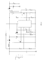
- the LED dimmer device includes rectifier, voltage boost device, pre-voltage detection circuit and after-voltage detection circuit adapted for detecting voltage, master chip adapted for driving circuit and elements to work, elementary transformer and secondary transformer adapter for changing voltage, secondary rectifier adapted for rectifying and secondary filter capacitance circuit adapter for filtering, and secondary switch.
- the rectifier is adapted for transforming alternating current into direct current.
- the voltage boost device includes a metal oxide semiconductor field effect transistor used to make dimmer entering into a normal phase-cutting state.
- the master chip includes integrated comparing element used to compare voltage.
- the secondary switch is used to drive transformer primary and secondary circuits, secondary rectifier, secondary filter capacitance circuit so as to drive LED light source to illuminate.
- the voltage booster device is adapted for enabling on-time current and on-time voltage of dimmer being in same phase mode, and having a relative lower peak value of current.
- the voltage of the pre-voltage detection circuit changes correspondingly, which acts as standard voltage to control brightness changing and is inputted to the master chip to control frequency and duty-cycle of secondary switch, then the primary and secondary circuits of transformer, secondary rectifier and secondary filter circuit are driven so as to drive LED light source to illuminate.
- the dimmer is any one of Si-controlled dimmer and electro-transistor dimmer.
- the number of the LED light source is one or more, and the LED light source is single color or multi-color.
- Si-controlled dimmer and electro-transistor dimmer may adjust brightness of LED light source such that environment friendly LED is more widely applied.
- the dimmer device has good the brightness adjusting efficiency.
- mains supply voltage is transformed into direct-current voltage via primary rectifier 1 and filter capacitance 2.
- the start-up resistance 9 firstly charges the master chip 10 so as to drive voltage boost device 5, 6, 7 to work.
- the voltage respectively detected by pre-voltage detection circuit 3, 4 and after-voltage detection circuit 11, 12 are simultaneously inputted to integrated comparator in the master chip 10 to compare, and then duty-cycle of metal oxide semiconductor field effect transistor (MOSFET) 7 of the step-up is adjusted to ensure that the voltage of step-up filter capacitance 8 is higher 30 volt-ampere than that of the filter capacitance 2.
- MOSFET metal oxide semiconductor field effect transistor
- the peak value current of the adapter is relative low and has the same on-time as the voltage waveform. Furthermore, the power factor can be over 0.8.
- switch tubes of step-up circuit is always in high frequency switch working state. The charge path of trigger circuit of the adapter is maintained, the adapter can be triggered again and works normally, which can be seen from waveform shown in FIG. 6 and FIG. 7 .
- the secondary switch 14 is driven by the master chip 10 to work.
- the pre-voltage detection circuit 3, 4 can detect change of voltage, which is also detection voltage of adapting information, and which is inputted to the master chip 10.
- Changing the duty-cycle of the secondary switch 14 adapts elementary charging current of the transformer.
- the secondary switch 14 is turned off, energy of transformer obtained by charging discharges to transformer secondary circuit 23. After acted by the secondary rectifier 24 and the secondary filter capacitance 25, the LED is driven to illuminate. Therefore, the brightness and driving current of the LED is controlled by the adapter such that the Si-controlled dimmer and electro-transistor dimmer can adjust the LED light source.
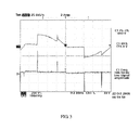
- FIG. 6 shows a schematic view of voltage and current waveform of a dimmer device adapted for use in dimmer according to a preferred embodiment according to the present invention.
- 1 indicates waveform rectified by electro-transistor dimmer, and the Si-controlled is adjusted to a lowest controlling angle, and the voltage thereof is 164 VDC.
- 2 indicates voltage waveform of the capacitance after step-up, and maximum of voltage is 210 VDC.
- 3 indicates alternating current waveform, in which current and voltage are in same mode and in same on-time. Maximum of current is 360 MA. 4 indicates driving waveform of MOSFET, of which frequency is 63 KHZ, and of which duty-cycle is 32%.
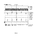
- FIG. 7 shows a schematic view of voltage and current waveform of a dimmer device adapted for use in dimmer according to a preferred embodiment according to the present invention.
- 1 indicates waveform rectified by Si-controlled dimmer, and the Si-controlled is adjusted to a lowest controlling angle, and the voltage thereof is 184 VDC.
- 2 indicates voltage waveform of the capacitance after step-up, and maximum of voltage is 250 VDC.
- 3 indicates alternating current waveform, in which current and voltage are in same phase mode and in same on-time. Maximum of current is 300 mA.
- 4 indicates driving waveform of MOSFET, of which frequency is 63 KHZ, and of which duty-cycle is 25%.
Description
- The present invention relates to a dimmer device, and more particularly pertains to a LED dimmer device adapted for use in dimmer.
- Si-controlled dimmer and electro-transistor dimmer (for short dimmer) can adjust brightness of tungsten lamp. Referring to
FIG. 1 , on-time of dimmer 5 is determined by charging time of capacitance 9 of circuit, and therefore change conduction angle of sinusoidal alternating current non-sinusoidal waveforms, and thus change current of thetungsten lamp 10 so as to adjust brightness, which is defined as leading edge technology. As indicated inFIG. 1 , dimmer 5 is connected withtungsten lamp 10 in series. Current passes through fuse 1,inductance 2,Potentiometer 7,resistance 8, capacitance 9, andtungsten lamp 10 to form a charging loop of charging capacitance 9. The charging time of the capacitance 9 is determined by resistance of thepotentiometer 7. When charging of the capacitance 9 is finished after a predetermined time, the capacitance 9 triggers control end of the dimmer 5 viatrigger diode 6 to make dimmer 5 conductive. Because thetungsten lamp 10 is resistance load, a voltage waveform 1 is consistent with current waveform 3 (referring toFIG. 2 ) after edge of dimmer, and the on-time is same as off-time. Therefore, the adjusting of brightness of thetungsten lamp 10 is achieved. - LED is energy-saving and new lamp. The power of LED is much smaller than tungsten lamp. LED is a low-voltage direct current element. LED lamp need to be equipped with a LED driving power supply so as to be drived to illuminate. LED driving-switch power supply is capacitive load and is not equipped with dimmer control circuit. When the
tungsten lamp 10 is replaced by LED lamp with switch power supply, the on-time of the dimmer 5 is shorter than that of voltage (referring toFIG. 3 ). When there is no current passing through the dimmer 5, there is voltage existed between theresistance 7 and the capacitance 9. This voltage charges for the capacitance 9. When charging for a predetermined time, the dimmer 5 is triggered, the dimmer 5 is in on-time twice in a half-period. LED lamp flashes frequently because of intermittence of input of driving-switch power supply. Therefore, the dimmer cannot adjust brightness of LED lamp with Internal/Extemal Auto-switch - Therefore, a dimmer device adapted for use in dimmer is desired to overcome the above-described shortcomings.
- Besides the above,
US-A-2005/0231133 in its figures 8-10 shows a conventional light source power supply, which employs a power factor correction apparatus between the rectifier and the DC-DC converter for adjusting the waveform and phase of the input voltage. Besides, the DC-DC converter of the power supply has a feedback-control loop as a power supply controller to receive the converter's output voltage and provide a control signal to a switch so as to adjust the amount of energy transferred across the transformer of the converter in a given time period. - It is therefore an object of the present invention to provide a dimmer device adapted for use in dimmer.
- The above object is achieved by the features of claim 1 of the present application.
- In one aspect, the LED dimmer device according to the invention includes rectifier, voltage boost device, pre-voltage detection circuit and after-voltage detection circuit adapted for detecting voltage, master chip adapted for driving circuit and elements to work, elementary transformer and secondary transformer adapter for changing voltage, secondary rectifier adapted for rectifying and secondary filter capacitance circuit adapter for filtering, and secondary switch. The rectifier is adapted for transforming alternating current into direct current. The voltage boost device includes a metal oxide semiconductor field effect transistor used to make dimmer entering into a normal phase-cutting state. The master chip includes integrated comparing element used to compare voltage. The secondary switch is used to drive transformer primary and secondary circuits, secondary rectifier, secondary filter capacitance circuit so as to drive LED light source to illuminate.
- In a further embodiment, the voltage booster device is adapted for enabling on-time current and on-time voltage of dimmer being in same phase mode, and having a relative lower peak value of current.
- In a further embodiment , when the alternating current rectified, voltage of the pre-voltage detection circuit and the after voltage detection circuit are simultaneously inputted to an integrated comparing element of the master chip, which control frequency and duty-cycle of the voltage boost device to insure that a difference between the step-up voltage and the voltage elementarily rectified is maintained at 30 volt.
- In a further embodiment , when the conducting angle of dimmer is changed, the voltage of the pre-voltage detection circuit changes correspondingly, which acts as standard voltage to control brightness changing and is inputted to the master chip to control frequency and duty-cycle of secondary switch, then the primary and secondary circuits of transformer, secondary rectifier and secondary filter circuit are driven so as to drive LED light source to illuminate.
- the dimmer is any one of Si-controlled dimmer and electro-transistor dimmer.
- In a further embodiment, the number of the LED light source is one or more, and the LED light source is single color or multi-color.
- According to the present invention, Si-controlled dimmer and electro-transistor dimmer may adjust brightness of LED light source such that environment friendly LED is more widely applied. The dimmer device has good the brightness adjusting efficiency.
- The components in the drawings are not necessarily drawn to scale, the emphasis instead being placed upon illustrating the principles of the present disclosure. Moreover, in the drawings, like reference numerals designate corresponding parts throughout several views, and all the views are schematic.
-
FIG. 1 is a conventional circuit principle view of Si-controlled dimmer adjusting brightness of tungsten lamp; -
FIG. 2 is a schematic view of voltage waveform and current waveform when Si-controlled dimmer being edged in adjusting brightness of tungsten lamp, in which 1 designates input alternating voltage waveform, 3 designates input alternating current waveform ; -
FIG. 3 is a schematic view of voltage waveform and current waveform when the tungsten lamp inFIG. 1 is replaced by LED lamp, in which 1 designates input alternating voltage, 3 designates input alternating current ; -
FIG. 4 is a circuit principle view of according to a embodiment according to the present invention ; -
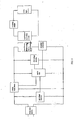
FIG. 5 is a flow-chart of a dimmer device adapted for use in dimmer according a embodiment according to the present invention; -
FIG. 6 is a schematic view of voltage and current waveform of a dimmer device adapted for use in dimmer according to a preferred embodiment according to the present invention; -
FIG. 7 is a schematic view of voltage and current waveform of a dimmer device adapted for use in dimmer according to a preferred embodiment according to the present invention. - The dimmer device adapted for use in dimmer will be described in detail with the following figures and embodiments. It is understood that the following detailed embodiments are used to explain the present invention, and not to limit the present invention.
- Referring to
FIG. 4 andFIG. 5 , after being phase-cut by a dimmer, mains supply voltage is transformed into direct-current voltage via primary rectifier 1 andfilter capacitance 2. The start-up resistance 9 firstly charges themaster chip 10 so as to drivevoltage boost device pre-voltage detection circuit master chip 10 to compare, and then duty-cycle of metal oxide semiconductor field effect transistor (MOSFET) 7 of the step-up is adjusted to ensure that the voltage of step-up filter capacitance 8 is higher 30 volt-ampere than that of thefilter capacitance 2. In addition, the peak value current of the adapter is relative low and has the same on-time as the voltage waveform. Furthermore, the power factor can be over 0.8. When the adapter is turn off, switch tubes of step-up circuit is always in high frequency switch working state. The charge path of trigger circuit of the adapter is maintained, the adapter can be triggered again and works normally, which can be seen from waveform shown inFIG. 6 andFIG. 7 . - The
secondary switch 14 is driven by themaster chip 10 to work. When controlling the angle of the knob adapter, thepre-voltage detection circuit master chip 10. Changing the duty-cycle of thesecondary switch 14 adapts elementary charging current of the transformer. When thesecondary switch 14 is turned off, energy of transformer obtained by charging discharges to transformersecondary circuit 23. After acted by thesecondary rectifier 24 and thesecondary filter capacitance 25, the LED is driven to illuminate. Therefore, the brightness and driving current of the LED is controlled by the adapter such that the Si-controlled dimmer and electro-transistor dimmer can adjust the LED light source. - Referring to
FIG. 6 , which shows a schematic view of voltage and current waveform of a dimmer device adapted for use in dimmer according to a preferred embodiment according to the present invention. InFIG. 6 ,1 indicates waveform rectified by electro-transistor dimmer, and the Si-controlled is adjusted to a lowest controlling angle, and the voltage thereof is 164 VDC. 2 indicates voltage waveform of the capacitance after step-up, and maximum of voltage is 210 VDC. 3 indicates alternating current waveform, in which current and voltage are in same mode and in same on-time. Maximum of current is 360 MA. 4 indicates driving waveform of MOSFET, of which frequency is 63 KHZ, and of which duty-cycle is 32%. - Referring to
FIG. 7 , which shows a schematic view of voltage and current waveform of a dimmer device adapted for use in dimmer according to a preferred embodiment according to the present invention. InFIG. 6 ,1 indicates waveform rectified by Si-controlled dimmer, and the Si-controlled is adjusted to a lowest controlling angle, and the voltage thereof is 184 VDC. 2 indicates voltage waveform of the capacitance after step-up, and maximum of voltage is 250 VDC. 3 indicates alternating current waveform, in which current and voltage are in same phase mode and in same on-time. Maximum of current is 300 mA. 4 indicates driving waveform of MOSFET, of which frequency is 63 KHZ, and of which duty-cycle is 25%. - Finally, while various embodiments have been described and illustrated, the disclosure is not to be construed as being limited thereto. Various modifications can be made to the embodiments by those skilled in the art.
Claims (6)
- A LED dimmer device adapted to be connected to a phase-cutting dimmer, comprising:a primary rectifier (1) adapted for converting an alternating current into a direct current;a voltage boost device (5-7) including a transistor (7) adapted to make the dimmer enter into a normal phase-cutting state;a pre-voltage detection circuit (3, 4) and an after-voltage detection circuit (11, 12) adapted for detecting an output voltage of the primary rectifier and an output voltage of the voltage boost device respectively;a master chip (10) adapted for driving circuits and elements of the device to work, the master chip including an integrated comparator adapted to compare voltages;a transformer including a primary circuit (13) and a secondary circuit (23), adapted for changing voltage, wherein the primary circuit (13) is connected to the output of the voltage boost device (5-7);a secondary rectifier (24) adapted for rectifying an output of said transformer;a secondary filter (25, 26) adapted for filtering the output of the transformer; anda secondary switch (14) adapted to driving said primary and secondary circuits of the transformer, the secondary rectifier and the secondary filter so as to be able to drive a LED light source to illuminate,
characterised in thatsaid transistor (7) of the voltage boost device (5-7) is a metal oxide semiconductor field effect transistor, andsaid master chip (10) is adapted for driving the secondary switch (14) based on the voltage detected by the pre-voltage detection circuit (3, 4). - The LED dimmer device of claim 1, wherein the voltage booster device is adapted for making an on-state current and an on-state voltage of the dimmer have same phase, and making the current have a relative lower peak value.
- The LED dimmer device of claim 2, wherein after the alternating current is rectified, the device is adapted for simultaneously inputting the voltage detected by the pre-voltage detection circuit and the voltage detected by the after-voltage detection circuit to said integrated comparator of the master chip so as to control a frequency and a duty-cycle of the voltage boost device to insure that a difference between the stepped-up voltage and the voltage elementarily rectified is maintained at 30 volt.
- The LED dimmer device of claim 3, wherein the device is adapted to a change in the conduction angle of the AC voltage of the phase cutting dimmer so that the voltage of the pre-voltage detection circuit changes correspondingly, which acting as a standard voltage for controlling a brightness change of the LED light source is adapted to be inputted to the master chip to control a frequency anda duty-cycle of the secondary switch such that the transformer, the secondary rectifier and the secondary Filter circuit are driven so as to be able to drive the LED light source to illuminate.
- Dimmer including a LED dimmer device of claim 1, wherein the dimmer is any one of a Si-controlled dimmer and an electro-transistor dimmer.
- LED assembly including the LED dimmer device of claim 1, wherein the LED light source comprises one or more LEDs, and the LED light source is single color or multi color.
Priority Applications (1)
| Application Number | Priority Date | Filing Date | Title |
|---|---|---|---|
| EP09159349.1A EP2249621B1 (en) | 2009-05-04 | 2009-05-04 | LED dimmer device adapted for use in dimmer |
Applications Claiming Priority (1)
| Application Number | Priority Date | Filing Date | Title |
|---|---|---|---|
| EP09159349.1A EP2249621B1 (en) | 2009-05-04 | 2009-05-04 | LED dimmer device adapted for use in dimmer |
Publications (2)
| Publication Number | Publication Date |
|---|---|
| EP2249621A1 EP2249621A1 (en) | 2010-11-10 |
| EP2249621B1 true EP2249621B1 (en) | 2014-04-30 |
Family
ID=40941658
Family Applications (1)
| Application Number | Title | Priority Date | Filing Date |
|---|---|---|---|
| EP09159349.1A Not-in-force EP2249621B1 (en) | 2009-05-04 | 2009-05-04 | LED dimmer device adapted for use in dimmer |
Country Status (1)
| Country | Link |
|---|---|
| EP (1) | EP2249621B1 (en) |
Families Citing this family (1)
| Publication number | Priority date | Publication date | Assignee | Title |
|---|---|---|---|---|
| GB2507308A (en) * | 2012-10-25 | 2014-04-30 | Spled Ltd | LED module driver |
Family Cites Families (3)
| Publication number | Priority date | Publication date | Assignee | Title |
|---|---|---|---|---|
| US6956336B2 (en) * | 2002-07-22 | 2005-10-18 | International Rectifier Corporation | Single chip ballast control with power factor correction |
| EP3223587A3 (en) | 2004-03-15 | 2017-11-08 | Philips Lighting North America Corporation | Power control methods and apparatus |
| KR100727354B1 (en) * | 2005-11-09 | 2007-06-13 | 주식회사 유양정보통신 | Constant Current Pulse Width Modulation Driving Circuit for Light Emitting Diode |
-
2009
- 2009-05-04 EP EP09159349.1A patent/EP2249621B1/en not_active Not-in-force
Also Published As
| Publication number | Publication date |
|---|---|
| EP2249621A1 (en) | 2010-11-10 |
Similar Documents
| Publication | Publication Date | Title |
|---|---|---|
| US8139378B2 (en) | LED dimmer device adapted for use in dimmer | |
| US8736194B2 (en) | LED dimmer circuit | |
| US9271347B2 (en) | TRIAC dimmable LED driver circuit | |
| US9419528B2 (en) | Trailing edge detector using current collapse | |
| CN101505568B (en) | LED light modulating apparatus suitable for light modulator | |
| US8872444B2 (en) | Lighting device for solid-state light source and illumination apparatus including same | |
| US8829819B1 (en) | Enhanced active preload for high performance LED driver with extended dimming | |
| US9049762B2 (en) | Constant voltage dimmable LED driver | |
| US8044600B2 (en) | Brightness-adjustable LED driving circuit | |
| US9112426B2 (en) | High power-factor control circuit and method for switched mode power supply | |
| TWI527494B (en) | Driving circuits, methods and controllers for driving light source | |
| EP2536013A2 (en) | A cascade boost and inverting buck converter with independent control | |
| EP2911474B1 (en) | High voltage converter without auxiliary winding | |
| US9750102B1 (en) | Switch current control to shape input current | |
| US20150312978A1 (en) | Multi-bleeder mode control for improved led driver performance | |
| TW201338627A (en) | Lighting power source and lighting apparatus | |
| WO2014179994A1 (en) | Power supply for led lamp with triac dimmer | |
| US9769890B1 (en) | Circuit and method for eliminating power-off flash for LED drivers | |
| CN102056378A (en) | Led driver with open loop dimming control | |
| EP3043624A1 (en) | LED driver with standby mode, and method for utlizing standby mode in a LED driver | |
| JP6278314B2 (en) | Lighting device and lighting apparatus using the same | |
| US8674615B2 (en) | Control apparatus for LED diodes | |
| WO2015161379A1 (en) | Dimmable led light | |
| JP2011120341A (en) | Power source circuit | |
| TW201401743A (en) | Constant current control buck converter without current sense |
Legal Events
| Date | Code | Title | Description |
|---|---|---|---|
| PUAI | Public reference made under article 153(3) epc to a published international application that has entered the european phase |
Free format text: ORIGINAL CODE: 0009012 |
|
| AK | Designated contracting states |
Kind code of ref document: A1 Designated state(s): AT BE BG CH CY CZ DE DK EE ES FI FR GB GR HR HU IE IS IT LI LT LU LV MC MK MT NL NO PL PT RO SE SI SK TR |
|
| AX | Request for extension of the european patent |
Extension state: AL BA RS |
|
| 17P | Request for examination filed |
Effective date: 20110510 |
|
| 17Q | First examination report despatched |
Effective date: 20110712 |
|
| RIC1 | Information provided on ipc code assigned before grant |
Ipc: H05B 33/08 20060101AFI20130429BHEP |
|
| GRAP | Despatch of communication of intention to grant a patent |
Free format text: ORIGINAL CODE: EPIDOSNIGR1 |
|
| INTG | Intention to grant announced |
Effective date: 20131210 |
|
| GRAS | Grant fee paid |
Free format text: ORIGINAL CODE: EPIDOSNIGR3 |
|
| GRAA | (expected) grant |
Free format text: ORIGINAL CODE: 0009210 |
|
| AK | Designated contracting states |
Kind code of ref document: B1 Designated state(s): AT BE BG CH CY CZ DE DK EE ES FI FR GB GR HR HU IE IS IT LI LT LU LV MC MK MT NL NO PL PT RO SE SI SK TR |
|
| REG | Reference to a national code |
Ref country code: GB Ref legal event code: FG4D Ref country code: CH Ref legal event code: EP |
|
| REG | Reference to a national code |
Ref country code: AT Ref legal event code: REF Ref document number: 665827 Country of ref document: AT Kind code of ref document: T Effective date: 20140515 |
|
| REG | Reference to a national code |
Ref country code: IE Ref legal event code: FG4D |
|
| REG | Reference to a national code |
Ref country code: DE Ref legal event code: R096 Ref document number: 602009023631 Country of ref document: DE Effective date: 20140612 |
|
| PGFP | Annual fee paid to national office [announced via postgrant information from national office to epo] |
Ref country code: GB Payment date: 20140630 Year of fee payment: 6 |
|
| PGFP | Annual fee paid to national office [announced via postgrant information from national office to epo] |
Ref country code: DE Payment date: 20140531 Year of fee payment: 6 |
|
| REG | Reference to a national code |
Ref country code: AT Ref legal event code: MK05 Ref document number: 665827 Country of ref document: AT Kind code of ref document: T Effective date: 20140430 |
|
| REG | Reference to a national code |
Ref country code: LT Ref legal event code: MG4D |
|
| REG | Reference to a national code |
Ref country code: NL Ref legal event code: VDEP Effective date: 20140430 |
|
| PG25 | Lapsed in a contracting state [announced via postgrant information from national office to epo] |
Ref country code: FI Free format text: LAPSE BECAUSE OF FAILURE TO SUBMIT A TRANSLATION OF THE DESCRIPTION OR TO PAY THE FEE WITHIN THE PRESCRIBED TIME-LIMIT Effective date: 20140430 Ref country code: GR Free format text: LAPSE BECAUSE OF FAILURE TO SUBMIT A TRANSLATION OF THE DESCRIPTION OR TO PAY THE FEE WITHIN THE PRESCRIBED TIME-LIMIT Effective date: 20140731 Ref country code: LT Free format text: LAPSE BECAUSE OF FAILURE TO SUBMIT A TRANSLATION OF THE DESCRIPTION OR TO PAY THE FEE WITHIN THE PRESCRIBED TIME-LIMIT Effective date: 20140430 Ref country code: NO Free format text: LAPSE BECAUSE OF FAILURE TO SUBMIT A TRANSLATION OF THE DESCRIPTION OR TO PAY THE FEE WITHIN THE PRESCRIBED TIME-LIMIT Effective date: 20140730 Ref country code: BG Free format text: LAPSE BECAUSE OF FAILURE TO SUBMIT A TRANSLATION OF THE DESCRIPTION OR TO PAY THE FEE WITHIN THE PRESCRIBED TIME-LIMIT Effective date: 20140730 Ref country code: IS Free format text: LAPSE BECAUSE OF FAILURE TO SUBMIT A TRANSLATION OF THE DESCRIPTION OR TO PAY THE FEE WITHIN THE PRESCRIBED TIME-LIMIT Effective date: 20140830 Ref country code: CY Free format text: LAPSE BECAUSE OF FAILURE TO SUBMIT A TRANSLATION OF THE DESCRIPTION OR TO PAY THE FEE WITHIN THE PRESCRIBED TIME-LIMIT Effective date: 20140430 Ref country code: NL Free format text: LAPSE BECAUSE OF FAILURE TO SUBMIT A TRANSLATION OF THE DESCRIPTION OR TO PAY THE FEE WITHIN THE PRESCRIBED TIME-LIMIT Effective date: 20140430 |
|
| PG25 | Lapsed in a contracting state [announced via postgrant information from national office to epo] |
Ref country code: HR Free format text: LAPSE BECAUSE OF FAILURE TO SUBMIT A TRANSLATION OF THE DESCRIPTION OR TO PAY THE FEE WITHIN THE PRESCRIBED TIME-LIMIT Effective date: 20140430 Ref country code: AT Free format text: LAPSE BECAUSE OF FAILURE TO SUBMIT A TRANSLATION OF THE DESCRIPTION OR TO PAY THE FEE WITHIN THE PRESCRIBED TIME-LIMIT Effective date: 20140430 Ref country code: PL Free format text: LAPSE BECAUSE OF FAILURE TO SUBMIT A TRANSLATION OF THE DESCRIPTION OR TO PAY THE FEE WITHIN THE PRESCRIBED TIME-LIMIT Effective date: 20140430 Ref country code: LV Free format text: LAPSE BECAUSE OF FAILURE TO SUBMIT A TRANSLATION OF THE DESCRIPTION OR TO PAY THE FEE WITHIN THE PRESCRIBED TIME-LIMIT Effective date: 20140430 Ref country code: ES Free format text: LAPSE BECAUSE OF FAILURE TO SUBMIT A TRANSLATION OF THE DESCRIPTION OR TO PAY THE FEE WITHIN THE PRESCRIBED TIME-LIMIT Effective date: 20140430 Ref country code: SE Free format text: LAPSE BECAUSE OF FAILURE TO SUBMIT A TRANSLATION OF THE DESCRIPTION OR TO PAY THE FEE WITHIN THE PRESCRIBED TIME-LIMIT Effective date: 20140430 |
|
| PGFP | Annual fee paid to national office [announced via postgrant information from national office to epo] |
Ref country code: FR Payment date: 20140630 Year of fee payment: 6 |
|
| PG25 | Lapsed in a contracting state [announced via postgrant information from national office to epo] |
Ref country code: PT Free format text: LAPSE BECAUSE OF FAILURE TO SUBMIT A TRANSLATION OF THE DESCRIPTION OR TO PAY THE FEE WITHIN THE PRESCRIBED TIME-LIMIT Effective date: 20140901 |
|
| REG | Reference to a national code |
Ref country code: CH Ref legal event code: PL |
|
| PG25 | Lapsed in a contracting state [announced via postgrant information from national office to epo] |
Ref country code: CH Free format text: LAPSE BECAUSE OF NON-PAYMENT OF DUE FEES Effective date: 20140531 Ref country code: LI Free format text: LAPSE BECAUSE OF NON-PAYMENT OF DUE FEES Effective date: 20140531 Ref country code: EE Free format text: LAPSE BECAUSE OF FAILURE TO SUBMIT A TRANSLATION OF THE DESCRIPTION OR TO PAY THE FEE WITHIN THE PRESCRIBED TIME-LIMIT Effective date: 20140430 Ref country code: MC Free format text: LAPSE BECAUSE OF FAILURE TO SUBMIT A TRANSLATION OF THE DESCRIPTION OR TO PAY THE FEE WITHIN THE PRESCRIBED TIME-LIMIT Effective date: 20140430 Ref country code: DK Free format text: LAPSE BECAUSE OF FAILURE TO SUBMIT A TRANSLATION OF THE DESCRIPTION OR TO PAY THE FEE WITHIN THE PRESCRIBED TIME-LIMIT Effective date: 20140430 Ref country code: SK Free format text: LAPSE BECAUSE OF FAILURE TO SUBMIT A TRANSLATION OF THE DESCRIPTION OR TO PAY THE FEE WITHIN THE PRESCRIBED TIME-LIMIT Effective date: 20140430 Ref country code: RO Free format text: LAPSE BECAUSE OF FAILURE TO SUBMIT A TRANSLATION OF THE DESCRIPTION OR TO PAY THE FEE WITHIN THE PRESCRIBED TIME-LIMIT Effective date: 20140430 Ref country code: BE Free format text: LAPSE BECAUSE OF FAILURE TO SUBMIT A TRANSLATION OF THE DESCRIPTION OR TO PAY THE FEE WITHIN THE PRESCRIBED TIME-LIMIT Effective date: 20140430 Ref country code: CZ Free format text: LAPSE BECAUSE OF FAILURE TO SUBMIT A TRANSLATION OF THE DESCRIPTION OR TO PAY THE FEE WITHIN THE PRESCRIBED TIME-LIMIT Effective date: 20140430 |
|
| REG | Reference to a national code |
Ref country code: DE Ref legal event code: R097 Ref document number: 602009023631 Country of ref document: DE |
|
| REG | Reference to a national code |
Ref country code: IE Ref legal event code: MM4A |
|
| PLBE | No opposition filed within time limit |
Free format text: ORIGINAL CODE: 0009261 |
|
| STAA | Information on the status of an ep patent application or granted ep patent |
Free format text: STATUS: NO OPPOSITION FILED WITHIN TIME LIMIT |
|
| PG25 | Lapsed in a contracting state [announced via postgrant information from national office to epo] |
Ref country code: IT Free format text: LAPSE BECAUSE OF FAILURE TO SUBMIT A TRANSLATION OF THE DESCRIPTION OR TO PAY THE FEE WITHIN THE PRESCRIBED TIME-LIMIT Effective date: 20140430 |
|
| 26N | No opposition filed |
Effective date: 20150202 |
|
| PG25 | Lapsed in a contracting state [announced via postgrant information from national office to epo] |
Ref country code: IE Free format text: LAPSE BECAUSE OF NON-PAYMENT OF DUE FEES Effective date: 20140504 |
|
| REG | Reference to a national code |
Ref country code: DE Ref legal event code: R097 Ref document number: 602009023631 Country of ref document: DE Effective date: 20150202 |
|
| PG25 | Lapsed in a contracting state [announced via postgrant information from national office to epo] |
Ref country code: SI Free format text: LAPSE BECAUSE OF FAILURE TO SUBMIT A TRANSLATION OF THE DESCRIPTION OR TO PAY THE FEE WITHIN THE PRESCRIBED TIME-LIMIT Effective date: 20140430 |
|
| REG | Reference to a national code |
Ref country code: DE Ref legal event code: R119 Ref document number: 602009023631 Country of ref document: DE |
|
| GBPC | Gb: european patent ceased through non-payment of renewal fee |
Effective date: 20150504 |
|
| REG | Reference to a national code |
Ref country code: FR Ref legal event code: ST Effective date: 20160129 |
|
| PG25 | Lapsed in a contracting state [announced via postgrant information from national office to epo] |
Ref country code: MT Free format text: LAPSE BECAUSE OF FAILURE TO SUBMIT A TRANSLATION OF THE DESCRIPTION OR TO PAY THE FEE WITHIN THE PRESCRIBED TIME-LIMIT Effective date: 20140430 |
|
| PG25 | Lapsed in a contracting state [announced via postgrant information from national office to epo] |
Ref country code: GB Free format text: LAPSE BECAUSE OF NON-PAYMENT OF DUE FEES Effective date: 20150504 Ref country code: DE Free format text: LAPSE BECAUSE OF NON-PAYMENT OF DUE FEES Effective date: 20151201 |
|
| PG25 | Lapsed in a contracting state [announced via postgrant information from national office to epo] |
Ref country code: FR Free format text: LAPSE BECAUSE OF NON-PAYMENT OF DUE FEES Effective date: 20150601 |
|
| PG25 | Lapsed in a contracting state [announced via postgrant information from national office to epo] |
Ref country code: LU Free format text: LAPSE BECAUSE OF NON-PAYMENT OF DUE FEES Effective date: 20140504 Ref country code: TR Free format text: LAPSE BECAUSE OF FAILURE TO SUBMIT A TRANSLATION OF THE DESCRIPTION OR TO PAY THE FEE WITHIN THE PRESCRIBED TIME-LIMIT Effective date: 20140430 Ref country code: HU Free format text: LAPSE BECAUSE OF FAILURE TO SUBMIT A TRANSLATION OF THE DESCRIPTION OR TO PAY THE FEE WITHIN THE PRESCRIBED TIME-LIMIT; INVALID AB INITIO Effective date: 20090504 |
|
| PG25 | Lapsed in a contracting state [announced via postgrant information from national office to epo] |
Ref country code: MK Free format text: LAPSE BECAUSE OF FAILURE TO SUBMIT A TRANSLATION OF THE DESCRIPTION OR TO PAY THE FEE WITHIN THE PRESCRIBED TIME-LIMIT Effective date: 20140430 |