EP2248026B1 - Memory system - Google Patents
Memory system Download PDFInfo
- Publication number
- EP2248026B1 EP2248026B1 EP09711527.3A EP09711527A EP2248026B1 EP 2248026 B1 EP2248026 B1 EP 2248026B1 EP 09711527 A EP09711527 A EP 09711527A EP 2248026 B1 EP2248026 B1 EP 2248026B1
- Authority
- EP
- European Patent Office
- Prior art keywords
- data
- information
- management
- management information
- writing
- Prior art date
- Legal status (The legal status is an assumption and is not a legal conclusion. Google has not performed a legal analysis and makes no representation as to the accuracy of the status listed.)
- Not-in-force
Links
- 230000015654 memory Effects 0.000 title claims description 253
- 238000007726 management method Methods 0.000 claims description 124
- 238000012545 processing Methods 0.000 claims description 119
- 238000013500 data storage Methods 0.000 claims description 15
- 238000000034 method Methods 0.000 claims description 15
- 238000002955 isolation Methods 0.000 claims description 14
- 230000008859 change Effects 0.000 claims description 13
- 230000002159 abnormal effect Effects 0.000 claims description 10
- 238000013523 data management Methods 0.000 claims description 7
- 230000008569 process Effects 0.000 claims description 7
- 238000007251 Prelog reaction Methods 0.000 description 26
- 238000010586 diagram Methods 0.000 description 23
- 238000012546 transfer Methods 0.000 description 13
- 238000006243 chemical reaction Methods 0.000 description 6
- 239000004065 semiconductor Substances 0.000 description 6
- 238000007667 floating Methods 0.000 description 5
- 238000005516 engineering process Methods 0.000 description 3
- 230000006870 function Effects 0.000 description 3
- 238000002360 preparation method Methods 0.000 description 3
- 239000000758 substrate Substances 0.000 description 3
- 238000001514 detection method Methods 0.000 description 2
- 230000000694 effects Effects 0.000 description 2
- 230000005669 field effect Effects 0.000 description 2
- 238000012986 modification Methods 0.000 description 2
- 230000004048 modification Effects 0.000 description 2
- 238000011084 recovery Methods 0.000 description 2
- 229910052581 Si3N4 Inorganic materials 0.000 description 1
- 238000009825 accumulation Methods 0.000 description 1
- 238000007796 conventional method Methods 0.000 description 1
- 238000009792 diffusion process Methods 0.000 description 1
- 230000000977 initiatory effect Effects 0.000 description 1
- 230000008439 repair process Effects 0.000 description 1
- 230000000630 rising effect Effects 0.000 description 1
- 230000011218 segmentation Effects 0.000 description 1
- HQVNEWCFYHHQES-UHFFFAOYSA-N silicon nitride Chemical compound N12[Si]34N5[Si]62N3[Si]51N64 HQVNEWCFYHHQES-UHFFFAOYSA-N 0.000 description 1
- 239000007787 solid Substances 0.000 description 1
- 230000003068 static effect Effects 0.000 description 1
Images


Classifications
-
- G—PHYSICS
- G06—COMPUTING; CALCULATING OR COUNTING
- G06F—ELECTRIC DIGITAL DATA PROCESSING
- G06F11/00—Error detection; Error correction; Monitoring
- G06F11/07—Responding to the occurrence of a fault, e.g. fault tolerance
- G06F11/14—Error detection or correction of the data by redundancy in operation
- G06F11/1402—Saving, restoring, recovering or retrying
- G06F11/1405—Saving, restoring, recovering or retrying at machine instruction level
- G06F11/141—Saving, restoring, recovering or retrying at machine instruction level for bus or memory accesses
-
- G—PHYSICS
- G06—COMPUTING; CALCULATING OR COUNTING
- G06F—ELECTRIC DIGITAL DATA PROCESSING
- G06F11/00—Error detection; Error correction; Monitoring
- G06F11/07—Responding to the occurrence of a fault, e.g. fault tolerance
- G06F11/14—Error detection or correction of the data by redundancy in operation
- G06F11/1402—Saving, restoring, recovering or retrying
- G06F11/1415—Saving, restoring, recovering or retrying at system level
- G06F11/1443—Transmit or communication errors
-
- G—PHYSICS
- G11—INFORMATION STORAGE
- G11C—STATIC STORES
- G11C11/00—Digital stores characterised by the use of particular electric or magnetic storage elements; Storage elements therefor
- G11C11/56—Digital stores characterised by the use of particular electric or magnetic storage elements; Storage elements therefor using storage elements with more than two stable states represented by steps, e.g. of voltage, current, phase, frequency
- G11C11/5621—Digital stores characterised by the use of particular electric or magnetic storage elements; Storage elements therefor using storage elements with more than two stable states represented by steps, e.g. of voltage, current, phase, frequency using charge storage in a floating gate
- G11C11/5628—Programming or writing circuits; Data input circuits
-
- G—PHYSICS
- G11—INFORMATION STORAGE
- G11C—STATIC STORES
- G11C16/00—Erasable programmable read-only memories
- G11C16/02—Erasable programmable read-only memories electrically programmable
- G11C16/04—Erasable programmable read-only memories electrically programmable using variable threshold transistors, e.g. FAMOS
- G11C16/0483—Erasable programmable read-only memories electrically programmable using variable threshold transistors, e.g. FAMOS comprising cells having several storage transistors connected in series
-
- G—PHYSICS
- G11—INFORMATION STORAGE
- G11C—STATIC STORES
- G11C16/00—Erasable programmable read-only memories
- G11C16/02—Erasable programmable read-only memories electrically programmable
- G11C16/06—Auxiliary circuits, e.g. for writing into memory
- G11C16/10—Programming or data input circuits
- G11C16/102—External programming circuits, e.g. EPROM programmers; In-circuit programming or reprogramming; EPROM emulators
- G11C16/105—Circuits or methods for updating contents of nonvolatile memory, especially with 'security' features to ensure reliable replacement, i.e. preventing that old data is lost before new data is reliably written
-
- G—PHYSICS
- G11—INFORMATION STORAGE
- G11C—STATIC STORES
- G11C29/00—Checking stores for correct operation ; Subsequent repair; Testing stores during standby or offline operation
- G11C29/04—Detection or location of defective memory elements, e.g. cell constructio details, timing of test signals
-
- G—PHYSICS
- G06—COMPUTING; CALCULATING OR COUNTING
- G06F—ELECTRIC DIGITAL DATA PROCESSING
- G06F11/00—Error detection; Error correction; Monitoring
- G06F11/07—Responding to the occurrence of a fault, e.g. fault tolerance
- G06F11/14—Error detection or correction of the data by redundancy in operation
- G06F11/1402—Saving, restoring, recovering or retrying
- G06F11/1471—Saving, restoring, recovering or retrying involving logging of persistent data for recovery
-
- G—PHYSICS
- G11—INFORMATION STORAGE
- G11C—STATIC STORES
- G11C29/00—Checking stores for correct operation ; Subsequent repair; Testing stores during standby or offline operation
Definitions
- the present invention relates to a memory system employing a nonvolatile semiconductor storage device.
- PC personal computers
- a hard disk device as a secondary storage device.
- a technology is known for backing up data that has been stored in the hard disk device to prevent the data from becoming invalid because of some failure. For example, when act of changing data in the hard disk device is detected, a snapshot as a backup copy of the data before the change is taken and a log of changes made to the data is generated. Then, processing for taking a new snapshot, invalidating a log taken in the past before the new snapshot was taken, and generating a new log is repeated at every predetermined time (see, for example, US Patent Application Publication No. 2006/0224636 ). In case data becomes invalid due to some reason, the data can be restored by referring to the snapshot and the log.
- a memory cell configuring a multi-value memory has a field effect transistor structure having a stacked gate structure in which a gate insulating film, a floating gate electrode, an inter-gate insulating film, and a control gate electrode are stacked in order on a channel region and a plurality of threshold voltages can be set according to the number of electrons accumulated in the floating gate electrode.
- the distribution of a threshold voltage corresponding to one data needs to be made extremely narrow.
- a multi-value memory that can store four values
- a method of writing data in such a multi-value memory after data is written in a lower order page of a first memory cell, data is written in a lower order page of a memory cell (a second memory cell) that is adjacent to the first memory cell. After data is written in this adjacent memory cell, data is written in a higher order page of the first memory cell (see, for example, JP-A 2004-192789 (KOKAI)).
- a threshold voltage of the first memory cell in which data has been written earlier fluctuates because of a threshold voltage of the second memory cell in which the data is written later and that is adjacent to the first memory cell. Therefore, in the multi-value memory, it is likely that lower order page breakage occurs in which, if writing is suspended because of, for example, abnormal isolation of a power supply (hereinafter referred to as a short break) while data is being written in a higher order page of a certain memory cell, data in a lower order page in which the data is written earlier is also broken.
- a short break abnormal isolation of a power supply
- WO2007/023674 A1 relates to a nonvolatile storage comprising a nonvolatile memory and a memory controller.
- the nonvolatile memory includes the same memory cells across a plurality of pages.
- a page information instruction unit has the page structure information of the nonvolatile memory. According to this information, a related page specifying unit specifies a page (related page) in which the data may change. The relation data stored in the related page are temporarily stored into a backup memory before an error occurs, and if an error is found, these relation data are used to repair the data that have changed.
- US2006/224636 A1 relates to systems and methods that facilitate providing page-level database restore functionality upon detection of a corruption event.
- Updates to a data page in a database can trigger generation of a snapshot of the data page, and an update log can be maintained that stores information related to page updates.
- Subsequent snapshots can be generated at predetermined intervals and can trigger truncation of a log segment and initiation of a new log segment.
- a most-recent uncorrupt snapshot of the corrupt page can be identified, copied to the location of the corrupt page in the database, and modified according to the log segment associated with the uncorrupt snapshot to make the page current as of the corrupting event, all of which can be performed to restore the database without having to take the database offline.
- a memory system comprises: a volatile first storing unit; a nonvolatile second storing unit in which a plurality of memory cells that can store multi-value data are arranged, the memory cells having a plurality of pages; and a controller that performs data transfer between a host apparatus and the second storing unit via the first storing unit, stores management information including a storage position of the data stored in the second storing unit during a startup operation of the memory system into the first storing unit, and performs, while updating stored management information, data management in the first and second storing units based on the stored management information.
- the controller includes a save processing unit that backs up, before writing data in the second storing unit in a write-once manner, if data has been already written in a lower order page of a memory cell same as that of a page in which the data is written, the data of the lower order page; and a broken-information-restoration processing unit that restores, when the data in the lower order page is broken, the broken data using the data backed-up by the save processing unit.
- a memory system includes a nonvolatile semiconductor storage device and is used as a secondary storage device (SSD: Solid State Drive) of a host apparatus such as a personal computer.
- the memory system has a function of storing data requested by a host apparatus to be written and reading out data requested by the host apparatus to be read out and outputting the data to the host apparatus.
- Fig. 1 is a block diagram of an example of a configuration of a memory system 10 according to the present embodiment.
- This memory system 10 includes a DRAM (Dynamic Random Access Memory) 11 as a first storing unit, a NAND flash memory (hereinafter, "NAND memory”) 12 as a second storing unit, a power supply circuit 13, and a drive control unit 14 as a controller.
- DRAM Dynamic Random Access Memory
- NAND memory NAND flash memory
- the DRAM 11 is used as a storing unit for data transfer, management information recording, or a work area. Specifically, when the DRAM 11 is used as a storing unit for data transfer, the DRAM 11 is used for temporarily storing data requested by the host apparatus to be written before the data is written in the NAND memory 12, and the DRAM 11 is used to read out data requested by the host apparatus to be read out from the NAND memory 12 and temporarily storing the read data.
- the DRAM 11 is used as a storing unit for management information recording, the DRAM 11 is used for storing management information for managing storage positions of data stored in the DRAM 11 and the NAND memory 12.
- the DRAM 11 is used, for example, during expansion of logs used when management information is restored.
- the NAND memory 12 is used as a storing unit for storing therein data. Specifically, the NAND memory 12 stores therein data designated by the host apparatus, stores therein, for backup, management information managed by the DRAM 11, and store therein the management program (firmware) of memory system 10.
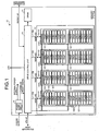
- the NAND memory 12 that includes four channel correspondence storage areas 120A to 120D has been shown as an example.
- Each of the channel correspondence storage areas 120A to 120D includes two packages 121 each including eight chips 122 having a storage capacity of a predetermined size (e.g., 2 GB).
- the channel correspondence storage areas 120A to 120D are connected via the drive control unit 14 and buses 15A to 15D. Each bus among the buses 15A to 15D connected to each of the channel correspondence storage areas 120A to 120D forms a channel.
- the power supply circuit 13 receives external power supply and generates a plurality of internal power supplies to be supplied to respective units of the memory system 10 from the external power supply.
- the power supply circuit 13 detects a state of the external power supply, i.e., a rising edge or a falling edge, generates a power-on reset signal based on the detected state, and outputs the power-on reset signal to the drive control unit 14.
- the drive control unit 14 controls the DRAM 11 and the NAND memory 12. As explained in detail later, for example, the drive control unit 14 performs restoration processing for management information and storage processing for management information according to the power-on reset signal from the power supply circuit 13.
- the drive control unit 14 transmits and receives data to and from a host apparatus via an ATA interface (I/F) and transmits and receives data to and from a debugging apparatus via an RS232C I/F. Furthermore, the drive control unit 14 outputs a control signal for controlling on/off of an LED for state display provided on the outside of the memory system 10.
- the NAND memory 12 is configured by arraying a plurality of blocks, which are units of data erasing, on a substrate.
- Fig. 2 is a circuit diagram of an example of a configuration of an arbitrary block of the NAND memory 12.
- left-right direction is set as an X direction and a direction perpendicular to the X direction is set as a Y direction.
- Each block BLK of the NAND memory 12 includes (m+1) (m is an integer equal to or larger than 0) NAND strings NS arrayed in order along the X direction.
- Each NAND string NS has (n+1) (n is an integer equal to or larger than 0) memory cell transistors MT0 to MTn that share a diffusion region (a source region or a drain region) between memory cell transistors MT adjacent to each other in the Y direction.
- the memory cell transistors MT0 to MTn are connected in series in the Y direction.
- selection transistors ST1 and ST2 arranged at both ends of a row of the (n+1) memory transistors MT0 to MTn.
- Each memory cell transistors MT0 to MTn is a field effect transistor having a stacked gate structure formed on a semiconductor substrate.
- the stacked gate structure includes a charge accumulation layer (a floating gate electrode) formed on the semiconductor substrate via a gate insulating film and a control gate electrode formed on the charge accumulating layer via an inter-gate insulating film.
- the memory cell transistors MT0 to MTn are multi-value memories in which a threshold voltage changes according to the number of electrons accumulated in the floating gate electrode and two or more bit data can be stored depending on the difference in the threshold voltage. It is assumed in following explanation that memory cell transistors MT0 to MTn are multi-value memories that can store quaternary values. However, the memory cell transistors MT0 to MTn can be multi-value memories that can store values larger than the quaternary values.
- Word lines WL0 to WLn are respectively connected to the control gate electrodes of the memory cell transistors MT0 to MTn of each NAND string NS.
- the control gate electrodes of the memory cell transistors MTi present on the same row in the block BLK are connected to the same word line WLi.
- a group of the (m+1) memory cell transistors MTi connected to the same word line WLi is a unit that forms one page.
- a group of the memory cell transistors MTi connected to the same word line WLi forms two pages.
- writing and readout of data is performed in units of the pages.
- Bit lines BL0 to BLm are respectively connected to drains of the (m+1) selection transistors ST1 in one block BLK.
- a selection gate line SGD is connected in common to gates of the selection transistors ST1 of each NAND string NS.
- Sources of the selection transistors ST1 are connected to drains of the memory cell transistors MT0.
- a source line SL is connected in common to sources of the (m+1) selection transistors ST2 in one block BLK.
- a selection gate line SGS is connected in common to gates of the selection transistors ST2 of each NAND string NS. Drains of the selection transistors ST2 are connected to sources of the memory cell transistors MTn.
- the NAND strings NS in the same column in the blocks BLK are connected by the same bit line BLj.
- the minimum unit for writing and readout is one page in the memory cell transistor MTi group connected to the same word line WLi and the minimum unit for erasing is one block including a predetermined number of pages (hereinafter referred to as physical block).
- a plurality of the blocks form a plane and a plurality of the planes form one channel correspondence storage areas 120A to 120D.
- a plurality of the channel correspondence storage areas 120A to 120D forms one NAND memory 12. In an example explained below, it is assumed that the number of channels is four and the number of planes is two.
- the channel correspondence storage areas 120A to 120D are connected in plurality to the drive control unit 14 in parallel to one another. Therefore, it is possible to actuate a plurality of channels in parallel, or actuate only one channel at a time.
- Writing and readout processing may be performed or erasing may be performed with a predetermined number of physical blocks as a unit according to setting of the drive control unit 14.
- a set of the predetermined number of physical blocks in this case is referred to as logical block.
- Fig. 3A is a schematic diagram of a functional configuration of the DRAM 11
- Fig. 3B is a schematic diagram of a functional configuration of the NAND memory 12.
- the DRAM 11 includes a write cache area in which data requested by the host apparatus to be written is stored, a read cache area RC in which data requested by the host apparatus to be read out is stored, a temporary storage area 111 in which management information for managing storage positions of data stored in the DRAM 11 and the NAND memory 12 is stored, and a work area 112 used when the management information is restored.
- the NAND memory 12 includes a data storage area 125 in which data requested by the host apparatus to be written is stored, a management information storage area 126 in which management information managed by the temporary storage area 111 of the DRAM 11 is stored, and a save area 127 in which contents of a lower order page are backed up to preserve the contents written in the lower order page from lower order page data breakage in which the lower order page is broken by occurrence of abnormal power supply isolation (short break) or a program error (failure in writing in a NAND memory) while data is written in a higher order page of a memory cell transistor in which the lower order page is already written.
- abnormal power supply isolation short break
- a program error failure in writing in a NAND memory
- the data storage area 125 of the NAND memory 12 is divided into a write-once area 128 in which data is written in a write-once manner and a non-write-once area 129 that is an area other than the write-once area 128 in the data storage area 125 and in which data is collectively written in a unit of one or a predetermined number of physical blocks.
- a data writing unit in the write-once area 128 is a page size unit
- a data writing unit in the non-write-once area 129 is a physical block size unit or an integer times as large as the physical block size unit. Therefore, in the data storage area 125, areas for storing blocks are further divided into areas in page size units and managed. The program error occurs when the memory cell transistor is broken and data cannot be stored.
- Fig. 4 is a diagram of an example of a layer structure for managing data stored in the memory system 10. It is assumed here that this data is the data requested by the host apparatus to be written or read out.
- data management is performed by a three-layer structure: a DRAM management layer 31, a logical NAND management layer 32, and a physical NAND management layer 33.
- the DRAM management layer 31 performs data management in the DRAM 11 that plays a role of a cache.
- the logical NAND management layer 32 performs logical data management in the NAND memory 12.
- the physical NAND management layer 33 performs physical data management in the NAND memory 12, life extension processing for the NAND memory 12, and the like.
- LBA Logical Block Address
- intra-DRAM physical address data designated by a logical address (hereinafter, "LBA (Logical Block Address)" managed by an address managing method of the host apparatus is stored in a physical address in a predetermined range on the DRAM 11 (hereinafter, "intra-DRAM physical address).
- Data in the DRAM management layer 31 is managed by cache management information 41 including a correspondence relation between an LBA of data to be stored and the intra-DRAM physical address and a sector flag indicating presence or absence of data in sector size units in a page.
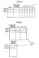
- Fig. 5 illustrates an example of the cache management information 41 in tabular manner.
- the cache management information 41 is one entry for one area of a one page size of the DRAM 11.
- the number of entries is equal to or smaller than the number of pages that fit in the write cache area WC and the read cache area RC.
- the LBA of data of a page size, the intra-DRAM physical address, and a sector flag indicating a position of valid data in each of areas obtained by dividing this page by a sector size are associated.
- NAND memory 12 data from the DRAM 11 is stored in a physical address in a predetermined range (hereinafter, "intra-NAND physical address) on the NAND memory 12.
- intra-NAND physical address a physical address in a predetermined range
- the drive control unit 14 performs control to equalize the numbers of times of rewriting among the blocks configuring the NAND memory 12 to write, in a block different from the original block, data reflecting a portion required to be updated of a block in which the data to be updated is included and invalidate the original block.
- intra-NAND logical address used independently in the NAND memory 12 (hereinafter, "intra-NAND logical address") is provided besides the intra-NAND physical address.
- data in the logical NAND management layer 32 is managed by logical NAND management information 42 indicating a relation between an LBA of data in page size units received from the DRAM 11 and an intra-NAND logical address indicating a logical page position of the NAND memory 12 in which the received data is stored and a relation indicating an address range of a logical block having a size coinciding with that of a block (hereinafter, "physical block") as an erasing unit in the NAND memory 12.
- a collection of a plurality of the physical blocks can be set as a logical block.
- logical-physical conversion information including a correspondence relation between the intra-NAND logical address as the logical block and the intra-NAND physical address as the physical block in the NAND memory 12.
- Fig. 6 illustrates an example of the logical NAND management information 42 in tabular manner.
- Fig. 7 illustrates an example of intra-NAND logical-physical conversion information 43 in tabular manner.
- the logical NAND management information 42 includes logical page management information 42a and logical block management information 42b.
- the logical page management information 42a has one entry for one logical area of a one page size. Each of entries includes an LBA of data of the one page size, an intra-NAND logical address, and a page flag indicating whether this page is valid.
- the logical block management information 42b includes an intra-NAND logical address set for a logical area of the one block size of the NAND memory 12.
- the logical page management information 42a and the logical block management information 42b are created for each of the data storage area 125 and the save area 127 and stored. As shown in Fig. 7 , in the intra-NAND logical-physical conversion information 43, the intra-NAND physical address and the inter-NAND logical address of the NAND memory 12 are associated.
- the management information managed by the DRAM management layer 31 is lost because of power-off or the like so that this management information can be called a volatile table.
- the management information managed by the logical NAND management layer 32 and the physical NAND management layer 33 is lost because of power-off or the like, the lost management information hinders successful startup of the memory system 10 so that measures are required to be taken such that the management information is stored even in the event of power-off or the like. Therefore, this management information can be called a nonvolatile table.
- This nonvolatile table manages data stored in the NAND memory 12. If the nonvolatile table is not present, information stored in the NAND memory 12 cannot be accessed or data stored in an area is erased. Therefore, the nonvolatile table needs to be stored as latest information in preparation for sudden power-off. Therefore, in the first embodiment, management information including at least the nonvolatile table is stored in the latest state in the management information storage area 126 of the NAND memory 12.
- the management information storage information stored in the management information storage area 126 of the NAND memory 12 is explained below. The following explanation assumes that only the nonvolatile table is stored in the management information storage area 126.
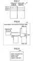
- Fig. 8 is a schematic diagram of an example of contents of the management information storage information stored in the management information storage area 126.
- the management information storage information stored in the management information storage information 126 includes a snapshot 210 as contents of the nonvolatile table at a certain point, a log 220 as difference information between the nonvolatile table after the contents are changed when there is a change in the contents of the nonvolatile table and the snapshot 210 (or the snapshot 210 and a log already generated), and a pointer 230 indicating positions of the snapshot 210 and the log 220 acquired first concerning the snapshot 210 are stored.
- the snapshot 210 is information obtained by storing management information including at least the nonvolatile table at a predetermined point among the management information stored in the temporary storage area 111 of the DRAM 11.
- the log 220 is generated before and after processing in which the management information changes (e.g., processing for writing data in the data storage area 125 of the NAND memory 12).
- a log stored before the processing is referred to as a pre-log 220A and a log stored after the processing is referred to as post-log 220B.
- the snapshot 210, the pre-log 220A, the post-log 220B, and the pointer 230 are stored in different blocks.
- the snapshot 210 is stored in a block for snapshot storage.
- the snapshot 210 includes the logical NAND management information 42 and the intra-NAND logical-physical conversion information 43 as nonvolatile tables in the management information storage area 126 of the NAND memory 12.
- a storage capacity of the NAND memory 12 is equal to or larger than several tens GB
- a size an integer times as large as the physical block is necessary as the size of management information necessary for data management. Therefore, this snapshot storing block is stored in a logical block including a plurality of physical blocks.
- the new snapshot 210 is collectively written in a block different from that for the snapshot 210 stored earlier.
- the pre-log 220A and the post-log 220B are stored in a pre-log storing block and a post-log storing block, respectively, in a write-once manner.
- the pre-log 220A and the post-log 220B are continuously written in the same pre-log storing block and the same post-log storing block, respectively, in a write-once manner even if a generation of the snapshot 210 changes.
- Each of the pre-log storing block and the post-log storing block includes a plurality of physical blocks.
- Fig. 9 is a diagram of an example of the log.
- the log 220 includes target information to be management information of a change target, a target entry as an entry to be a change target in the target information, a target item as an item to be a change target in the target entry, and change contents as contents of a change of the target item.
- the pointer 230 is stored in an instruction information storage block.
- the pointer 230 only has to be a pointer that indicates a top address of a block indicating storage positions of the snapshot 210, the pre-log 220A, and the post-log 220B.
- a portion indicating a storage position of the snapshot 210 in the pointer 230 can be a portion that indicates top addresses of respective kinds of management information included in the snapshot 210.
- the pointer 230 is updated when the snapshot 210 is stored anew or when the physical block storing the log 220 in a log storing block is changed. Pointers of the pre-log 220A and the post-log 220B can be stored in the snapshot 210 rather than in the instruction information storing block.
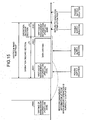
- Fig. 10 is a block diagram of an example of a functional configuration of the drive control unit.
- the drive control unit 14 includes a data managing unit 141, an ATA command processing unit 142, a security managing unit 143, a boot loader 144, an initialization managing unit 145, and a debug support unit 146.
- the data managing unit 141 performs data transfer between the DRAM 11 and the NAND memory 12 and control of various functions concerning the NAND memory 12.
- the ATA command processing unit 142 performs data transfer processing in cooperation with the data managing unit 141 based on an instruction received from the ATA interface.
- the security managing unit 143 manages various kinds of security information in cooperation with the data managing unit 141 and the ATA command processing unit 142.
- the boot loader 144 loads management programs (firmware) from the NAND memory 12 to a not shown memory (e.g., an SRAM (Static RAM)) during power-on.
- the initialization managing unit 145 performs initialization of respective controllers and circuits in the drive control unit 14.
- the debug support unit 146 processes debug data supplied from the outside via the RS232C interface.
- Fig. 11 is a block diagram of an example of a functional configuration of the data managing unit 141.
- the data managing unit 141 includes a data-transfer processing unit 151, a management-information managing unit 152, a save processing unit 155, a broken-information-restoration processing unit 156, and a management-information restoring unit 157.
- the data-transfer processing unit 151 performs data transfer between the DRAM 11 and the NAND memory 12.
- the management-information managing unit 152 performs change and storage of the management information according to a change in data stored in the DRAM 11 and the NAND memory 12.
- the save processing unit 155 saves, in the save area 127, data likely to be broken by lower order page data breakage during write-once processing of data in the write-once area 128.
- the broken-information-restoration processing unit 156 restores information broken by lower order page data breakage during the write-once processing of data in the write-once area 128 using the data in the save area 127.
- the management-information restoring unit 157 restores latest management information based on the management information stored in the NAND memory 12 during power-on or the like.
- the management-information managing unit 152 includes a management-information writing unit 153 and a management-information storing unit 154.
- the management-information writing unit 153 performs update of the management information stored in the DRAM 11 when update of the management information is necessary according to the change processing for data stored in the DRAM 11 or the NAND memory 12 by the data-transfer processing unit 151.
- the management-information storing unit 154 stores, in the management information storage area 126 of the NAND memory 12, the management information as the snapshot 210 or stores information to be updated in the management information as the log 220.
- the management-information storing unit 154 also performs update processing for the pointer 230.
- Storing of the snapshot 210 is performed by the management-information storing unit 154 when a predetermined condition relating to the memory system 10 is satisfied. Storing of the snapshot 210 is performed, for example, when a log storage area provided to store the log 220 (the pre-log 220A and the post-log 220B) in the management information storage area 126 of the NAND memory 12 becomes full (i.e., the area is completely filled with data).
- Storing of the log 220 is performed by the management-information storing unit 154 during data update (when data writing in the NAND memory 12 is necessary) on the NAND memory 12 involving update of the management information (the nonvolatile table) stored in the DRAM 11.
- the save processing unit 155 When write data is written in the write-once area 128 by the data-transfer processing unit 151 or the management-information storing unit 154, if a page in which the write data is written is a different page (a higher order page) of a memory cell transistor same as that for a written page in which data is already written, the save processing unit 155 performs processing for storing the written data stored in the written page in the save area 127 in preparation for occurrence of lower order page data breakage due to occurrence of a short break or a program error during writing of the write data.
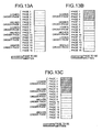
- Figs. 12A to 12D are diagrams of examples of a relation between data in a memory cell and a threshold voltage of the memory cell and order of writing in a NAND memory.
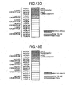
- Figs. 13A to 13E are diagrams for explaining lower order page data breakage during write-once processing.
- the data in the memory cell is set to "0" when an erasing operation is performed.
- the data in the memory cell changes to data "0" and data "2".
- Fig. 12B before writing in a higher order page, data equal to or lower than a threshold voltage of actual data is written in an adjacent cell.
- a distribution of a threshold of the data "2" is expanded by the data written in the cell. Thereafter, when data of the higher order page is written, the data in the memory cell changes to data "0" to "3" having an original threshold voltage as shown in Fig. 12C .
- the data in the memory cell is defined from low to high threshold voltages.
- a writing operation is performed for each of pages from a memory cell close to a source line in a block.
- a source line in a block For convenience of explanation, four word lines are shown.
- first writing In first writing (indicated by encircled 1), 1-bit data is written in a lower order page of a memory cell 1.
- second writing In second writing (indicated by encircled 2), 1-bit data is written in a lower order page of a memory cell 2 adjacent to the memory cell 1 in a word line direction.
- third writing In third writing (indicated by encircled 3), 1-bit data is written in a lower order page of a memory cell 3 adjacent to the memory cell 1 in a bit line direction.
- fourth writing In fourth writing (indicated by encircled 4), 1-bit data is written in a lower order page of a memory cell 4 diagonally adjacent to the memory cell 1.
- 1-bit data is written in a higher order page of the memory cell 5.
- 1-bit data is written in a higher order page of the memory cell 6 adjacent to the memory cell 5 in the word line direction.
- 1-bit data is written in a higher order page of the memory cell 7.
- sixteenth writing is written in a higher order page of the memory cell 8 adjacent to the memory cell 7 in the word line direction.
- the save processing unit 155 stores, as page position information, a relation between the lower order pages and the higher order pages explained above, i.e., a relation between the lower order pages and the higher order pages that are likely to cause lower order page data breakage.
- Pages in one physical block in Fig. 13A correspond to Figs. 12A to 12D .
- pages 1 to 4, 7 to 8, and 11 to 12 are the lower order pages shown in Figs. 12A to 12D .
- Pages 5 to 6, 9 to 10, and 13 to 16 are the higher order pages shown in Figs. 12A to 12D .
- the write-once processing for writing in a block having such a page structure performed when save processing is necessary and the write-once processing performed when the save processing is unnecessary are separately explained below.
- pages are separated into lower order pages and higher order pages for convenience of explanation. However, a combination of the lower order pages and the higher order pages forms one physical block.
- the save processing is unnecessary when data is written only in the lower order pages (e.g., pages 1 to 4) in a write-once manner. This is because, in this case, lower order page data breakage does not occur even if a short break occurs while the data is written in the lower order pages.
- the save processing is necessary when data is written in the lower order pages and the higher order pages not including written pages. This is because, in this case, the data is written in the lower order pages 1 to 4 and the higher order pages 5 to 6 and lower order page data breakage does not occur because the lower order pages 1 and 2 corresponding to the higher order pages 5 and 6 are not written pages.
- the broken-information-restoration processing unit 156 performs processing for restoring data in a position where the lower order page data breakage occurs using the data saved in the save area 127.
- the management-information restoring unit 157 When the power supply of the memory system 10 is turned on, the management-information restoring unit 157 performs restoration processing for the management information based on the management information storage information stored in the management information storage area 126 of the NAND memory 12. Specifically, the management-information restoring unit 157 traces the pointer 230 and the log 220 (the pre-log 220A or the post-log 220B) in order and determines whether the log 220 (the pre-log 220A or the post-log 220B) corresponding to the latest snapshot 210 is present. When the log 220 is not present, the management-information restoring unit 157 restores the snapshot 210 in the snapshot storing block in the DRAM 11 as management information.
- the management-information restoring unit 157 acquires the snapshot 210 from the snapshot storing block, acquires the log 220 (the pre-log 220A or the post-log 220B) from the log storing block, and performs restoration of the management information (the nonvolatile table) reflecting the log 220 on the snapshot 210 on the DRAM 11.
- FIG. 14 is a flowchart of an example of a procedure of processing for writing data in the write-once area of the memory system. It is assumed that the memory system 10 is connected to the host apparatus and operates as the secondary storage device of the host apparatus and the host apparatus (the memory system 10) is in a startup state.
- the save processing unit 155 When the memory system 10 is in the started state, the save processing unit 155.receives an instruction for write-once processing for data (Step S11). The save processing unit 155 acquires a writing position for the data to be subjected to the write-once processing (hereinafter referred to as write data) (Step S12). Subsequently, the save processing unit 155 determines whether a part of the acquired writing position includes a higher order page and determines whether a lower order page corresponding to the higher order page is a written page (Step S13).
- the save processing unit 155 acquires, using the page position information, a lower order page that uses a memory cell same as that for the higher order page in the writing position (Step S14). Subsequently, the management-information managing unit 152 determines an update schedule (including processing for storage in the save area 127) for the management information by execution of the write-once processing (Step S15) and stores the update schedule in the management information storage area 126 of the NAND memory 12 as the pre-log 220A (Step S16).
- the save processing unit 155 stores contents of data stored in the lower order page acquired at Step S14 in the save area 127 (Step S17).
- the data-transfer processing unit 151 saves the post-log 220B in the management information storage area 126 of the NAND memory 12 (Step S19) and the write-once processing for the data ends.
- the management-information managing unit 152 determines an update schedule for the management information by execution of the write-once processing (Step S20) and stores the update schedule in the management information storage area 126 of the NAND memory 12 as the pre-log 220A (Step S21). Thereafter, after writing the write data in the writing position in a write-once manner (Step S22), the data-transfer processing unit 151 saves the post-log 220B in the management information storage area 126 of the NAND memory 12 (Step S23) and the write-once processing for the data ends.
- FIG. 15 is a diagram for explaining an example of a rule for matching the data in the NAND memory and the management information in the write-once processing.
- the abscissa indicates elapsed time t.
- Step S300 after write processing for the post-log 220B with respect to any one of the kinds of processing explained above ends (Step S300), write processing (storage) for the pre-log 220A (Step S301), write-once processing for write data (Step S302), and write processing (storage) for the post-log 220B (Step S303) are performed for the next write-once processing.
- Step S301 When a short break occurs from the write processing for the pre-log 220A (Step S301) to the write-once processing for the write data (Step S302), the processing for writing the write data in the NAND memory 12 has not ended properly due to the short break.
- the processing for writing the write data in the NAND memory 12 has not ended properly due to the short break.
- the operation performed until a time point at which the short break occurred is discarded.
- a time span in which the operation is discarded is referred to as an operation discard section D1.
- Step S302 when the write-once processing for the write data (Step S302) ends and a short break occurs at a stage after the write processing for the post-log 220B (Step S303), the processing for writing the write data in the NAND memory 12 has ended properly.
- the operation until the occurrence of the short break is not discarded and the contents written in the pre-log 220A are adopted as management information, no problem occurs because the write data has been already written in the NAND memory 12. Therefore, in this case, operation that was being executed during the time span in which the short break continued is decided.
- a time span in which the operation is decided is referred to as an operation decision section D2.
- Figs. 16 are 17 are flowcharts of an example of restoration processing for write data after occurrence of a short break. As in the above explanation, it is assumed that the memory system 10 is connected to the host apparatus and operates as the secondary storage device of the host apparatus.
- Step S31 the power supply of the host apparatus is turned on and a startup instruction is issued to the memory system 10 (Step S31).
- the boot loader 144 shown in Fig. 10 transfers a not-shown management program from the NAND memory 12 to a memory such as an SRAM or the DRAM 11 (Step S32) and starts the management program (Step S33).
- Step S32 the management program
- Step S33 the management program
- processing by the respective functional processing units in the data managing unit 141 shown in Fig. 11 can be performed.
- the management-information restoring unit 157 reads the latest pointer 230 in the management information storage area 126 of the NAND memory 12 and acquires addresses of blocks in which the snapshot 210 and the pre-log 220A and the post-log 220B are stored (Step S34).
- the management-information restoring unit 157 reads the snapshot 210 from the address in the NAND memory 12 acquired at Step S34 and restores the snapshot 210 in the temporary storage area 111 of the DRAM 11 (Step S35).
- the management-information restoring unit 157 checks a last writing position of a log referring to the pre-log 220A and the post-log 220B in the NAND memory 12 and compares writable page positions to detect a log written last and timing for power supply isolation (Step S36). Thereafter, the management-information restoring unit 157 determines whether a short break has occurred (Step S37). In determining whether a short break has occurred, the management-information restoring unit 157 compares the number of pages from a writing position to a last writing position of the first pre-log 220A generated for the reference snapshot 210 and the number of pages from a writing position to a last writing position of the first post-log 220B generated in the same manner.
- the management-information restoring unit 157 determines that a short break has occurred. Otherwise, the management-information restoring unit 157 determines that a short break has not occurred.
- the management-information restoring unit 157 compares contents of the logs written last. When the contents are the same, the management-information restoring unit 157 determines that a short break has not occurred. Otherwise, the management-information restoring unit 157 determines that a short break has occurred.
- the management-information restoring unit 157 restores the management information from the snapshot 210 restored in the temporary storage area 111 of the DRAM 11 at Step S35 (Step S38) and the restoration processing ends.
- the management-information restoring unit 157 determines whether a section where the short break has occurred is the operation discard section D1 (Step S39). When the section where the short break has occurred is not the operation discard section D1, i.e., when the section where the short break has occurred is the operation decision section D2 ("No" at Step S39), the management-information restoring unit 157 expands the pre-log 220A present in the storage position acquired at Step S34 in the work area 112 of the DRAM 11 (Step S40). The management-information restoring unit 157 reflects logs on the snapshot 210 in order from the oldest pre-log 220A and restores the management information (Step S41) and the restoration processing ends.
- the management-information restoring unit 157 expands the post-log 220B present in the storage position acquired at Step S34 in the work area 112 of the DRAM 11 (Step S42) and determines whether there is data being written in the save area 127 in a write-once manner (Step S43).
- the management-information restoring unit 157 determines whether there is data being written in the write-once area 128 in a write-once manner (Step S44).
- Step S44 When there is data being written in the write-once area 128 in a write-once manner ("Yes" at Step S44), it means that the power supply isolation is power supply isolation during the write-once processing for writing in a lower order page; therefore, the management-information restoring unit 157 determines that there is no breakage of data in the past by lower order page data breakage (Step S45). The management-information restoring unit 157 invalidates a relevant page or copies a valid page of a relevant block to a block secured anew (Step S46).
- the management-information restoring unit 157 reflects logs on the snapshot 210 in order from the oldest post-log 220B expanded in the DRAM 11 at Step S42 to the post-log 220B at a stage before the discard processing and restores the management information (Step S47) and the restoration processing ends.
- the management-information restoring unit 157 determines that the short break has occurred at a time point before the write-once processing is performed (Step S48). Therefore, recovery processing for the data in the write-once area 128 is unnecessary.
- the management-information restoring unit 157 reflects logs on the snapshot 210 in order from the oldest post-log 220B expanded in the DRAM 11 at Step S42 and restores the management information (Step S49) and the restoration processing ends.
- the management-information restoring unit 157 When there is data being written in the save area 127 in a write-once manner at Step S43 ("Yes" at Step S43), the management-information restoring unit 157 further checks whether there is data being written in the write-once area 128 in a write-once manner (Step S50). When there is data being written in the write-once area 128 in a write-once manner ("Yes” at Step S50), it means that the power supply isolation is power supply isolation during the write-once processing for writing in a higher order page; therefore, the management-information restoring unit 157 determines that breakage of data in the past due to lower order page data breakage is likely to occur (Step S51).
- the management-information restoring unit 157 restores a broken page in the write-once area 128 from the backup in the save area 127 and copies the page to a block secured anew (Step S.52).
- the management-information restoring unit 157 reflects logs on the snapshot 210 in order from the oldest post-log 220B expanded in the DRAM 11 at Step S42 and restores the management information (Step S53) and the restoration processing ends.
- the management-information restoring unit 157 reflects logs on the snapshot 210 in order from the oldest post-log 220B expanded in the DRAM 11 at Step S42 and restores the management information (Step S55) and the restoration processing ends. In this case, the management-information restoring unit 157 performs processing for disabling writing of contents of a page being written in the save area 127 in a write-once manner. According to the procedure explained above, the restoration processing at the time of occurrence of a short break with respect to the write-once data ends.
- the processing for writing in the higher order page is performed after contents of data stored in a lower order page of a multi-value memory cell same as that of the higher order page to be subjected to the write-once processing are stored in the save area 127. Therefore, there is an effect that, even when lower order page data breakage occurs because of occurrence of a short break or occurrence of a program error during the write processing, it is possible to restore data broken by the lower order page data breakage using the data stored in the save area 127..
- the memory cell transistor MT forming the NAND memory 12 is the multi-value memory equal to or larger than 2 bits.
- pages include three or more pages such as a higher order page, an intermediate page, and a lower order page. During writing in the higher order page, it is likely that lower order page data breakage occurs in the intermediate page and the lower order page. In that case, data in the intermediate page and the lower order page are stored in the save area 127.
- the save area 127 is provided in the NAND memory 12.
- a dedicated storing unit for the save area 127 may be provided in a nonvolatile memory of a type different from the NAND memory 12.
- the charge accumulating layer is not limited to the floating gate type and can be a charge trap type including a silicon nitride film such as the MONOS (Metal-Oxide-Nitride-Oxide-Semiconductor) structure and other systems.
Description
- The present invention relates to a memory system employing a nonvolatile semiconductor storage device.
- Some personal computers (PC) employ a hard disk device as a secondary storage device. In such PCs, a technology is known for backing up data that has been stored in the hard disk device to prevent the data from becoming invalid because of some failure. For example, when act of changing data in the hard disk device is detected, a snapshot as a backup copy of the data before the change is taken and a log of changes made to the data is generated. Then, processing for taking a new snapshot, invalidating a log taken in the past before the new snapshot was taken, and generating a new log is repeated at every predetermined time (see, for example,
US Patent Application Publication No. 2006/0224636 ). In case data becomes invalid due to some reason, the data can be restored by referring to the snapshot and the log. - In recent years, a capacity of a NAND flash memory as a nonvolatile semiconductor storage device has been increased dramatically. As a result, PCs including a memory system having the NAND flash memory as a secondary storage device have been put to practical use.
- However, the technology disclosed in
US Patent Application Publication No. 2006/0224636 cannot be applied to backup of data stored in such a personal computer having the NAND flash memory as the secondary storage device as in the case of backup of data stored in the personal computer having the hard disk device as the secondary storage device. This is because a multi-value memory technology that can store a plurality of data (multi-value data) equal to or larger than 2 bits in one memory cell is employed to increase the capacity of the NAND flash memory. - A memory cell configuring a multi-value memory has a field effect transistor structure having a stacked gate structure in which a gate insulating film, a floating gate electrode, an inter-gate insulating film, and a control gate electrode are stacked in order on a channel region and a plurality of threshold voltages can be set according to the number of electrons accumulated in the floating gate electrode. In order to make it possible to perform multi-value storage based on the plurality of threshold voltages, the distribution of a threshold voltage corresponding to one data needs to be made extremely narrow.
- For example, as a multi-value memory that can store four values, there is a multi-value memory that includes a lower order page and a higher order page in one memory cell and stores 2 bits (four values) by writing 1-bit data in the respective pages. In a method of writing data in such a multi-value memory, after data is written in a lower order page of a first memory cell, data is written in a lower order page of a memory cell (a second memory cell) that is adjacent to the first memory cell. After data is written in this adjacent memory cell, data is written in a higher order page of the first memory cell (see, for example,
JP-A 2004-192789 - However, in such a multi-value memory, a threshold voltage of the first memory cell in which data has been written earlier fluctuates because of a threshold voltage of the second memory cell in which the data is written later and that is adjacent to the first memory cell. Therefore, in the multi-value memory, it is likely that lower order page breakage occurs in which, if writing is suspended because of, for example, abnormal isolation of a power supply (hereinafter referred to as a short break) while data is being written in a higher order page of a certain memory cell, data in a lower order page in which the data is written earlier is also broken.
- Therefore, in the personal computer having the NAND flash memory as the secondary storage device, for example, when the lower order page data breakage occurs because of a short break while the log is written in a higher order page of a certain memory cell as disclosed in
US Patent Application Publication No. 2006/0224636 , there is a problem in that, not only the data that is currently being written is broken, even data in a lower order page of the memory cell in which data is being currently written is broken and the data cannot be restored. In other words, there is a problem in that the method of taking backup using the technique disclosed inUS Patent Publication No. 2006/0224636 for the personal computer including the memory system having the NAND flash memory as the secondary storage device is insufficient for restoring a state of the personal computer to a state before a short break. - In particular, when the memory system is started next time after a short break occurs during writing in a higher order page of a certain memory transistor, in the conventional method, a state of the memory system cannot be reset to a latest state before the short break occurs. Processing for restoring the memory system to the latest state when a short break occurs is not proposed.
-
WO2007/023674 A1 relates to a nonvolatile storage comprising a nonvolatile memory and a memory controller. The nonvolatile memory includes the same memory cells across a plurality of pages. A page information instruction unit has the page structure information of the nonvolatile memory. According to this information, a related page specifying unit specifies a page (related page) in which the data may change. The relation data stored in the related page are temporarily stored into a backup memory before an error occurs, and if an error is found, these relation data are used to repair the data that have changed. -
US2006/224636 A1 relates to systems and methods that facilitate providing page-level database restore functionality upon detection of a corruption event. Updates to a data page in a database can trigger generation of a snapshot of the data page, and an update log can be maintained that stores information related to page updates. Subsequent snapshots can be generated at predetermined intervals and can trigger truncation of a log segment and initiation of a new log segment. Upon detection of page corruption, a most-recent uncorrupt snapshot of the corrupt page can be identified, copied to the location of the corrupt page in the database, and modified according to the log segment associated with the uncorrupt snapshot to make the page current as of the corrupting event, all of which can be performed to restore the database without having to take the database offline. - A memory system according to an embodiment of the present invention comprises: a volatile first storing unit; a nonvolatile second storing unit in which a plurality of memory cells that can store multi-value data are arranged, the memory cells having a plurality of pages; and a controller that performs data transfer between a host apparatus and the second storing unit via the first storing unit, stores management information including a storage position of the data stored in the second storing unit during a startup operation of the memory system into the first storing unit, and performs, while updating stored management information, data management in the first and second storing units based on the stored management information. The controller includes a save processing unit that backs up, before writing data in the second storing unit in a write-once manner, if data has been already written in a lower order page of a memory cell same as that of a page in which the data is written, the data of the lower order page; and a broken-information-restoration processing unit that restores, when the data in the lower order page is broken, the broken data using the data backed-up by the save processing unit.
-
-
Fig. 1 is a block diagram of an example of a configuration of a memory system according to a first embodiment of the present invention; -
Fig. 2 is a circuit diagram of an example of a configuration of an arbitrary block of a NAND memory; -
Fig. 3A is a schematic diagram of a functional configuration of a DRAM andFig. 3B is a schematic diagram of a functional configuration of the NAND memory; -
Fig. 4 is a diagram of an example of a layer structure for managing data stored in the memory system; -
Fig. 5 illustrates an example of a cache management information table; -
Fig. 6 illustrates an example of a logical NAND management information table; -
Fig. 7 illustrates an example of an intra-NAND logical-physical conversion information table; -
Fig. 8 is a schematic diagram of an example of contents of management information storage information stored in a management information storage area according to the first embodiment; -
Fig. 9 depicts an example of a log; -
Fig. 10 is a block diagram of an example of a functional configuration of a drive control unit shown inFig. 1 ; -
Fig. 11 is a block diagram of an example of a functional configuration of a data managing unit shown inFig. 11 ; -
Figs. 12A to 12D are diagrams of examples of a relation between data in a memory cell and a threshold voltage of the memory cell and order of writing in a NAND memory; -
Figs. 13A to 13E are diagrams for explaining lower order page data breakage during write-once processing; -
Fig. 14 is a flowchart of an example of a procedure of processing for writing data in a write-once area of the memory system; -
Fig. 15 is a diagram of an example of a rule for aligning data in the NAND memory and management information in the write-once processing; and -
Figs. 16 and17 are flowcharts of an example of restoration processing for write data after occurrence of a short break. - Exemplary embodiments of a memory system according to the present invention are explained in detail below with reference to the accompanying drawings. The present invention is not limited by this embodiment.
- A memory system according to an embodiment of the present invention includes a nonvolatile semiconductor storage device and is used as a secondary storage device (SSD: Solid State Drive) of a host apparatus such as a personal computer. The memory system has a function of storing data requested by a host apparatus to be written and reading out data requested by the host apparatus to be read out and outputting the data to the host apparatus.
Fig. 1 is a block diagram of an example of a configuration of amemory system 10 according to the present embodiment. Thismemory system 10 includes a DRAM (Dynamic Random Access Memory) 11 as a first storing unit, a NAND flash memory (hereinafter, "NAND memory") 12 as a second storing unit, apower supply circuit 13, and adrive control unit 14 as a controller. - The
DRAM 11 is used as a storing unit for data transfer, management information recording, or a work area. Specifically, when theDRAM 11 is used as a storing unit for data transfer, theDRAM 11 is used for temporarily storing data requested by the host apparatus to be written before the data is written in theNAND memory 12, and theDRAM 11 is used to read out data requested by the host apparatus to be read out from theNAND memory 12 and temporarily storing the read data. When theDRAM 11 is used as a storing unit for management information recording, theDRAM 11 is used for storing management information for managing storage positions of data stored in theDRAM 11 and theNAND memory 12. When theDRAM 11 is used as a storing unit for a work area, theDRAM 11 is used, for example, during expansion of logs used when management information is restored. - The
NAND memory 12 is used as a storing unit for storing therein data. Specifically, theNAND memory 12 stores therein data designated by the host apparatus, stores therein, for backup, management information managed by theDRAM 11, and store therein the management program (firmware) ofmemory system 10. InFig. 1 , theNAND memory 12 that includes four channelcorrespondence storage areas 120A to 120D has been shown as an example. Each of the channelcorrespondence storage areas 120A to 120D includes twopackages 121 each including eightchips 122 having a storage capacity of a predetermined size (e.g., 2 GB). The channelcorrespondence storage areas 120A to 120D are connected via thedrive control unit 14 andbuses 15A to 15D. Each bus among thebuses 15A to 15D connected to each of the channelcorrespondence storage areas 120A to 120D forms a channel. - The
power supply circuit 13 receives external power supply and generates a plurality of internal power supplies to be supplied to respective units of thememory system 10 from the external power supply. Thepower supply circuit 13 detects a state of the external power supply, i.e., a rising edge or a falling edge, generates a power-on reset signal based on the detected state, and outputs the power-on reset signal to thedrive control unit 14. - The
drive control unit 14 controls theDRAM 11 and theNAND memory 12. As explained in detail later, for example, thedrive control unit 14 performs restoration processing for management information and storage processing for management information according to the power-on reset signal from thepower supply circuit 13. Thedrive control unit 14 transmits and receives data to and from a host apparatus via an ATA interface (I/F) and transmits and receives data to and from a debugging apparatus via an RS232C I/F. Furthermore, thedrive control unit 14 outputs a control signal for controlling on/off of an LED for state display provided on the outside of thememory system 10. - A configuration of the
NAND memory 12 is explained in detail below. TheNAND memory 12 is configured by arraying a plurality of blocks, which are units of data erasing, on a substrate.Fig. 2 is a circuit diagram of an example of a configuration of an arbitrary block of theNAND memory 12. InFig. 2 , left-right direction is set as an X direction and a direction perpendicular to the X direction is set as a Y direction. - Each block BLK of the
NAND memory 12 includes (m+1) (m is an integer equal to or larger than 0) NAND strings NS arrayed in order along the X direction. Each NAND string NS has (n+1) (n is an integer equal to or larger than 0) memory cell transistors MT0 to MTn that share a diffusion region (a source region or a drain region) between memory cell transistors MT adjacent to each other in the Y direction. Moreover, the memory cell transistors MT0 to MTn are connected in series in the Y direction. In addition, selection transistors ST1 and ST2 arranged at both ends of a row of the (n+1) memory transistors MT0 to MTn. - Each memory cell transistors MT0 to MTn is a field effect transistor having a stacked gate structure formed on a semiconductor substrate. The stacked gate structure includes a charge accumulation layer (a floating gate electrode) formed on the semiconductor substrate via a gate insulating film and a control gate electrode formed on the charge accumulating layer via an inter-gate insulating film. Moreover, the memory cell transistors MT0 to MTn are multi-value memories in which a threshold voltage changes according to the number of electrons accumulated in the floating gate electrode and two or more bit data can be stored depending on the difference in the threshold voltage. It is assumed in following explanation that memory cell transistors MT0 to MTn are multi-value memories that can store quaternary values. However, the memory cell transistors MT0 to MTn can be multi-value memories that can store values larger than the quaternary values.
- Word lines WL0 to WLn are respectively connected to the control gate electrodes of the memory cell transistors MT0 to MTn of each NAND string NS. Memory cell transistors MTi (i=0 to n) in each of the NAND strings NS are connected in common by the same word lines (i=0 to n). In other words, the control gate electrodes of the memory cell transistors MTi present on the same row in the block BLK are connected to the same word line WLi. Specifically, a group of the (m+1) memory cell transistors MTi connected to the same word line WLi is a unit that forms one page. In the case of the multi-value memory that can store quaternary values, a group of the memory cell transistors MTi connected to the same word line WLi forms two pages. When a page in which data is written first is set as a lower order page and a page in which data is written next is set as a higher order page, in the
NAND memory 12, writing and readout of data is performed in units of the pages. - Bit lines BL0 to BLm are respectively connected to drains of the (m+1) selection transistors ST1 in one block BLK. A selection gate line SGD is connected in common to gates of the selection transistors ST1 of each NAND string NS. Sources of the selection transistors ST1 are connected to drains of the memory cell transistors MT0. Similarly, a source line SL is connected in common to sources of the (m+1) selection transistors ST2 in one block BLK. A selection gate line SGS is connected in common to gates of the selection transistors ST2 of each NAND string NS. Drains of the selection transistors ST2 are connected to sources of the memory cell transistors MTn.
- Although not shown in the figure, bit lines BLj (j=0 to m) in one block BLK connect drains of the selection transistors ST1 in common between bit lines BLj of other blocks BLK. In other words, the NAND strings NS in the same column in the blocks BLK are connected by the same bit line BLj.
- In the
NAND memory 12, as explained above, the minimum unit for writing and readout is one page in the memory cell transistor MTi group connected to the same word line WLi and the minimum unit for erasing is one block including a predetermined number of pages (hereinafter referred to as physical block). A plurality of the blocks form a plane and a plurality of the planes form one channelcorrespondence storage areas 120A to 120D. A plurality of the channelcorrespondence storage areas 120A to 120D forms oneNAND memory 12. In an example explained below, it is assumed that the number of channels is four and the number of planes is two. - In this memory system, the channel
correspondence storage areas 120A to 120D are connected in plurality to thedrive control unit 14 in parallel to one another. Therefore, it is possible to actuate a plurality of channels in parallel, or actuate only one channel at a time. - Writing and readout processing may be performed or erasing may be performed with a predetermined number of physical blocks as a unit according to setting of the
drive control unit 14. A set of the predetermined number of physical blocks in this case is referred to as logical block. - Functional configurations of the
DRAM 11 and theNAND memory 12 are explained next.Fig. 3A is a schematic diagram of a functional configuration of theDRAM 11 andFig. 3B is a schematic diagram of a functional configuration of theNAND memory 12. As shown inFig. 3A , theDRAM 11 includes a write cache area in which data requested by the host apparatus to be written is stored, a read cache area RC in which data requested by the host apparatus to be read out is stored, atemporary storage area 111 in which management information for managing storage positions of data stored in theDRAM 11 and theNAND memory 12 is stored, and awork area 112 used when the management information is restored. - As shown in
Fig. 3B , theNAND memory 12 includes adata storage area 125 in which data requested by the host apparatus to be written is stored, a managementinformation storage area 126 in which management information managed by thetemporary storage area 111 of theDRAM 11 is stored, and asave area 127 in which contents of a lower order page are backed up to preserve the contents written in the lower order page from lower order page data breakage in which the lower order page is broken by occurrence of abnormal power supply isolation (short break) or a program error (failure in writing in a NAND memory) while data is written in a higher order page of a memory cell transistor in which the lower order page is already written. Thedata storage area 125 of theNAND memory 12 is divided into a write-once area 128 in which data is written in a write-once manner and a non-write-once area 129 that is an area other than the write-once area 128 in thedata storage area 125 and in which data is collectively written in a unit of one or a predetermined number of physical blocks. In this example, it is assumed that a data writing unit in the write-once area 128 is a page size unit and a data writing unit in the non-write-once area 129 is a physical block size unit or an integer times as large as the physical block size unit. Therefore, in thedata storage area 125, areas for storing blocks are further divided into areas in page size units and managed. The program error occurs when the memory cell transistor is broken and data cannot be stored. - The management information managed in the
temporary storage area 111 of theDRAM 11 is explained below.Fig. 4 is a diagram of an example of a layer structure for managing data stored in thememory system 10. It is assumed here that this data is the data requested by the host apparatus to be written or read out. In thememory system 10, data management is performed by a three-layer structure: aDRAM management layer 31, a logicalNAND management layer 32, and a physicalNAND management layer 33. TheDRAM management layer 31 performs data management in theDRAM 11 that plays a role of a cache. The logicalNAND management layer 32 performs logical data management in theNAND memory 12. The physicalNAND management layer 33 performs physical data management in theNAND memory 12, life extension processing for theNAND memory 12, and the like. - In the write cache area WC and the read cache area RC of the
DRAM 11, data designated by a logical address (hereinafter, "LBA (Logical Block Address)") managed by an address managing method of the host apparatus is stored in a physical address in a predetermined range on the DRAM 11 (hereinafter, "intra-DRAM physical address). Data in theDRAM management layer 31 is managed bycache management information 41 including a correspondence relation between an LBA of data to be stored and the intra-DRAM physical address and a sector flag indicating presence or absence of data in sector size units in a page. -
Fig. 5 illustrates an example of thecache management information 41 in tabular manner. Thecache management information 41 is one entry for one area of a one page size of theDRAM 11. The number of entries is equal to or smaller than the number of pages that fit in the write cache area WC and the read cache area RC. In each of the entries, the LBA of data of a page size, the intra-DRAM physical address, and a sector flag indicating a position of valid data in each of areas obtained by dividing this page by a sector size are associated. - In the
NAND memory 12, data from theDRAM 11 is stored in a physical address in a predetermined range (hereinafter, "intra-NAND physical address) on theNAND memory 12. In theNAND memory 12 formed by the multi-value memory, because the number of rewritable times is limited, the numbers of times of rewriting among the blocks configuring theNAND memory 12 are controlled by thedrive control unit 14 to be equalized. In other words, when update of data written in a certain intra-NAND physical address in theNAND memory 12 is performed, thedrive control unit 14 performs control to equalize the numbers of times of rewriting among the blocks configuring theNAND memory 12 to write, in a block different from the original block, data reflecting a portion required to be updated of a block in which the data to be updated is included and invalidate the original block. - As explained above, in the
NAND memory 12, processing units are different in the writing and readout processing for data and the erasing processing for data. In the update processing for data, a position (a block) of data before update and a position (a block) of data after update are different. Therefore, in the first embodiment, an intra-NAND logical address used independently in the NAND memory 12 (hereinafter, "intra-NAND logical address") is provided besides the intra-NAND physical address. - Therefore, data in the logical
NAND management layer 32 is managed by logicalNAND management information 42 indicating a relation between an LBA of data in page size units received from theDRAM 11 and an intra-NAND logical address indicating a logical page position of theNAND memory 12 in which the received data is stored and a relation indicating an address range of a logical block having a size coinciding with that of a block (hereinafter, "physical block") as an erasing unit in theNAND memory 12. A collection of a plurality of the physical blocks can be set as a logical block. Data in the physicalNAND management layer 33 is managed by intra-NAND logical address-physical address conversion information (hereinafter, "logical-physical conversion information") including a correspondence relation between the intra-NAND logical address as the logical block and the intra-NAND physical address as the physical block in theNAND memory 12. -
Fig. 6 illustrates an example of the logicalNAND management information 42 in tabular manner.Fig. 7 illustrates an example of intra-NAND logical-physical conversion information 43 in tabular manner. As shown inFig. 6 , the logicalNAND management information 42 includes logicalpage management information 42a and logicalblock management information 42b. The logicalpage management information 42a has one entry for one logical area of a one page size. Each of entries includes an LBA of data of the one page size, an intra-NAND logical address, and a page flag indicating whether this page is valid. The logicalblock management information 42b includes an intra-NAND logical address set for a logical area of the one block size of theNAND memory 12. - The logical
page management information 42a and the logicalblock management information 42b are created for each of thedata storage area 125 and thesave area 127 and stored. As shown inFig. 7 , in the intra-NAND logical-physical conversion information 43, the intra-NAND physical address and the inter-NAND logical address of theNAND memory 12 are associated. - By using these kinds of management information, a correspondence of the LBA used in the host apparatus, the intra-NAND logical address used in the
NAND memory 12, and the intra-NAND physical address used in theNAND memory 12 can be established. This makes it is possible to exchange data between the host apparatus and thememory system 10. - The management information managed by the
DRAM management layer 31 is lost because of power-off or the like so that this management information can be called a volatile table. On the contrary, if the management information managed by the logicalNAND management layer 32 and the physicalNAND management layer 33 is lost because of power-off or the like, the lost management information hinders successful startup of thememory system 10 so that measures are required to be taken such that the management information is stored even in the event of power-off or the like. Therefore, this management information can be called a nonvolatile table. - This nonvolatile table manages data stored in the
NAND memory 12. If the nonvolatile table is not present, information stored in theNAND memory 12 cannot be accessed or data stored in an area is erased. Therefore, the nonvolatile table needs to be stored as latest information in preparation for sudden power-off. Therefore, in the first embodiment, management information including at least the nonvolatile table is stored in the latest state in the managementinformation storage area 126 of theNAND memory 12. The management information storage information stored in the managementinformation storage area 126 of theNAND memory 12 is explained below. The following explanation assumes that only the nonvolatile table is stored in the managementinformation storage area 126. -
Fig. 8 is a schematic diagram of an example of contents of the management information storage information stored in the managementinformation storage area 126. The management information storage information stored in the managementinformation storage information 126 includes asnapshot 210 as contents of the nonvolatile table at a certain point, alog 220 as difference information between the nonvolatile table after the contents are changed when there is a change in the contents of the nonvolatile table and the snapshot 210 (or thesnapshot 210 and a log already generated), and apointer 230 indicating positions of thesnapshot 210 and thelog 220 acquired first concerning thesnapshot 210 are stored. Thesnapshot 210 is information obtained by storing management information including at least the nonvolatile table at a predetermined point among the management information stored in thetemporary storage area 111 of theDRAM 11. Thelog 220 is generated before and after processing in which the management information changes (e.g., processing for writing data in thedata storage area 125 of the NAND memory 12). A log stored before the processing is referred to as a pre-log 220A and a log stored after the processing is referred to aspost-log 220B. - The
snapshot 210, the pre-log 220A, the post-log 220B, and thepointer 230 are stored in different blocks. Thesnapshot 210 is stored in a block for snapshot storage. Thesnapshot 210 includes the logicalNAND management information 42 and the intra-NAND logical-physical conversion information 43 as nonvolatile tables in the managementinformation storage area 126 of theNAND memory 12. In general, when a storage capacity of theNAND memory 12 is equal to or larger than several tens GB, a size an integer times as large as the physical block is necessary as the size of management information necessary for data management. Therefore, this snapshot storing block is stored in a logical block including a plurality of physical blocks. Thenew snapshot 210 is collectively written in a block different from that for thesnapshot 210 stored earlier. - The pre-log 220A and the post-log 220B are stored in a pre-log storing block and a post-log storing block, respectively, in a write-once manner. The pre-log 220A and the post-log 220B are continuously written in the same pre-log storing block and the same post-log storing block, respectively, in a write-once manner even if a generation of the
snapshot 210 changes. Each of the pre-log storing block and the post-log storing block includes a plurality of physical blocks.Fig. 9 is a diagram of an example of the log. - The
log 220 includes target information to be management information of a change target, a target entry as an entry to be a change target in the target information, a target item as an item to be a change target in the target entry, and change contents as contents of a change of the target item. - The
pointer 230 is stored in an instruction information storage block. Thepointer 230 only has to be a pointer that indicates a top address of a block indicating storage positions of thesnapshot 210, the pre-log 220A, and the post-log 220B. However, a portion indicating a storage position of thesnapshot 210 in thepointer 230 can be a portion that indicates top addresses of respective kinds of management information included in thesnapshot 210. Thepointer 230 is updated when thesnapshot 210 is stored anew or when the physical block storing thelog 220 in a log storing block is changed. Pointers of the pre-log 220A and the post-log 220B can be stored in thesnapshot 210 rather than in the instruction information storing block. - Functions of the
drive control unit 14 are explained below.Fig. 10 is a block diagram of an example of a functional configuration of the drive control unit. Thedrive control unit 14 includes adata managing unit 141, an ATAcommand processing unit 142, asecurity managing unit 143, aboot loader 144, aninitialization managing unit 145, and adebug support unit 146. Thedata managing unit 141 performs data transfer between theDRAM 11 and theNAND memory 12 and control of various functions concerning theNAND memory 12. The ATAcommand processing unit 142 performs data transfer processing in cooperation with thedata managing unit 141 based on an instruction received from the ATA interface. Thesecurity managing unit 143 manages various kinds of security information in cooperation with thedata managing unit 141 and the ATAcommand processing unit 142. Theboot loader 144 loads management programs (firmware) from theNAND memory 12 to a not shown memory (e.g., an SRAM (Static RAM)) during power-on. Theinitialization managing unit 145 performs initialization of respective controllers and circuits in thedrive control unit 14. Thedebug support unit 146 processes debug data supplied from the outside via the RS232C interface. -
Fig. 11 is a block diagram of an example of a functional configuration of thedata managing unit 141. Thedata managing unit 141 includes a data-transfer processing unit 151, a management-information managing unit 152, asave processing unit 155, a broken-information-restoration processing unit 156, and a management-information restoring unit 157. The data-transfer processing unit 151 performs data transfer between theDRAM 11 and theNAND memory 12. The management-information managing unit 152 performs change and storage of the management information according to a change in data stored in theDRAM 11 and theNAND memory 12. The save processingunit 155 saves, in thesave area 127, data likely to be broken by lower order page data breakage during write-once processing of data in the write-once area 128. The broken-information-restoration processing unit 156 restores information broken by lower order page data breakage during the write-once processing of data in the write-once area 128 using the data in thesave area 127. The management-information restoring unit 157 restores latest management information based on the management information stored in theNAND memory 12 during power-on or the like. - The management-
information managing unit 152 includes a management-information writing unit 153 and a management-information storing unit 154. The management-information writing unit 153 performs update of the management information stored in theDRAM 11 when update of the management information is necessary according to the change processing for data stored in theDRAM 11 or theNAND memory 12 by the data-transfer processing unit 151. - When the
memory system 10 satisfies a predetermined condition, the management-information storing unit 154 stores, in the managementinformation storage area 126 of theNAND memory 12, the management information as thesnapshot 210 or stores information to be updated in the management information as thelog 220. When a position where thepointer 230 is written is changed according to the storage of thesnapshot 210 or the log 220 (the pre-log 220A and the post-log 220B), the management-information storing unit 154 also performs update processing for thepointer 230. - Storing of the
snapshot 210 is performed by the management-information storing unit 154 when a predetermined condition relating to thememory system 10 is satisfied. Storing of thesnapshot 210 is performed, for example, when a log storage area provided to store the log 220 (the pre-log 220A and the post-log 220B) in the managementinformation storage area 126 of theNAND memory 12 becomes full (i.e., the area is completely filled with data). - Storing of the log 220 (the pre-log 220A and the post-log 220B) is performed by the management-
information storing unit 154 during data update (when data writing in theNAND memory 12 is necessary) on theNAND memory 12 involving update of the management information (the nonvolatile table) stored in theDRAM 11. - When write data is written in the write-
once area 128 by the data-transfer processing unit 151 or the management-information storing unit 154, if a page in which the write data is written is a different page (a higher order page) of a memory cell transistor same as that for a written page in which data is already written, the save processingunit 155 performs processing for storing the written data stored in the written page in thesave area 127 in preparation for occurrence of lower order page data breakage due to occurrence of a short break or a program error during writing of the write data. -
Figs. 12A to 12D are diagrams of examples of a relation between data in a memory cell and a threshold voltage of the memory cell and order of writing in a NAND memory.Figs. 13A to 13E are diagrams for explaining lower order page data breakage during write-once processing. First, the data in the memory cell is set to "0" when an erasing operation is performed. Subsequently, as shown inFig. 12A , when writing in a lower order page is performed, the data in the memory cell changes to data "0" and data "2". As shown inFig. 12B , before writing in a higher order page, data equal to or lower than a threshold voltage of actual data is written in an adjacent cell. Then, a distribution of a threshold of the data "2" is expanded by the data written in the cell. Thereafter, when data of the higher order page is written, the data in the memory cell changes to data "0" to "3" having an original threshold voltage as shown inFig. 12C . In the present embodiment, the data in the memory cell is defined from low to high threshold voltages. - Writing processing in the
NAND memory 12 is explained below. As shown inFig. 12D , a writing operation is performed for each of pages from a memory cell close to a source line in a block. InFig. 12D , for convenience of explanation, four word lines are shown. - In first writing (indicated by encircled 1), 1-bit data is written in a lower order page of a
memory cell 1. In second writing (indicated by encircled 2), 1-bit data is written in a lower order page of amemory cell 2 adjacent to thememory cell 1 in a word line direction. In third writing (indicated by encircled 3), 1-bit data is written in a lower order page of amemory cell 3 adjacent to thememory cell 1 in a bit line direction. In fourth writing (indicated by encircled 4), 1-bit data is written in a lower order page of amemory cell 4 diagonally adjacent to thememory cell 1. - In fifth writing (indicated by encircled 5), 1-bit data is written in a higher order page of the
memory cell 1. In sixth writing (indicated by encircled 6), 1-bit data is written in a higher order page of thememory cell 2 adjacent to thememory cell 1 in the word line direction. In seventh writing (indicated by encircled 7), 1-bit data is written in a lower order page of amemory cell 5 adjacent to thememory cell 3 in the bit line direction. In eighth writing (indicated by encircled 8), 1-bit data is written in a lower order page of amemory cell 6 diagonally adjacent to thememory cell 3. - In ninth writing (indicated by encircled 9), 1-bit data is written in a higher order page of the
memory cell 3. In tenth writing (indicated by encircled 10), 1-bit data is written in a higher order page of thememory cell 4 adjacent to thememory cell 3 in the word line direction. In eleventh writing (indicated by encircled 11), 1-bit data is written in a lower order page of amemory cell 7 adjacent to thememory cell 5 in the bit line direction. In twelfth writing (indicated by encircled 12), 1-bit data is written in a lower order page of amemory cell 8 diagonally adjacent to thememory cell 5. - In thirteenth writing (indicated by encircled 13), 1-bit data is written in a higher order page of the
memory cell 5. In fourteenth writing (indicated by encircled 14), 1-bit data is written in a higher order page of thememory cell 6 adjacent to thememory cell 5 in the word line direction. In fifteenth writing (indicated by encircled 15), 1-bit data is written in a higher order page of thememory cell 7. In sixteenth writing (indicated by encircled 16), 1-bit data is written in a higher order page of thememory cell 8 adjacent to thememory cell 7 in the word line direction. - The save processing
unit 155 stores, as page position information, a relation between the lower order pages and the higher order pages explained above, i.e., a relation between the lower order pages and the higher order pages that are likely to cause lower order page data breakage. - Pages in one physical block in
Fig. 13A correspond toFigs. 12A to 12D . In other words,pages 1 to 4, 7 to 8, and 11 to 12 are the lower order pages shown inFigs. 12A to 12D .Pages 5 to 6, 9 to 10, and 13 to 16 are the higher order pages shown inFigs. 12A to 12D . The write-once processing for writing in a block having such a page structure performed when save processing is necessary and the write-once processing performed when the save processing is unnecessary are separately explained below. InFigs. 13A to 13E , pages are separated into lower order pages and higher order pages for convenience of explanation. However, a combination of the lower order pages and the higher order pages forms one physical block. - As shown in
Fig. 13B , the save processing is unnecessary when data is written only in the lower order pages (e.g.,pages 1 to 4) in a write-once manner. This is because, in this case, lower order page data breakage does not occur even if a short break occurs while the data is written in the lower order pages. - As shown in
Fig. 13C , the save processing is necessary when data is written in the lower order pages and the higher order pages not including written pages. This is because, in this case, the data is written in thelower order pages 1 to 4 and thehigher order pages 5 to 6 and lower order page data breakage does not occur because thelower order pages higher order pages - As shown in
Fig. 13D , when data is written only in the higher order pages in a write-once manner, the lower order pages are always written pages. In this case, lower order pages in which lower page data breakage is likely to be caused by higher order pages in which write data is written are calculated from page position information. Contents stored in the lower order pages are saved in thesave area 127. This is because, in this processing, when a short break occurs during writing in higher order pages, it is likely that lower order pages corresponding thereto (i.e., lower order pages of a memory cell transistor same as that for the higher order pages in which data is written) are broken. In the case illustrated inFig. 13D , when writing is performed in thehigher order pages lower order pages 1 are 2 are saved in thesave area 127 from the page position information shown inFigs. 12A to 12D . - As shown in
Fig. 13E , when data is written in the lower order pages and the higher order pages including written pages, lower order pages in which lower page data breakage is likely to be caused by higher order pages in which data to be written in the higher order pages among the data is written are calculated from page position information. Contents stored in the lower order pages are saved in thesave area 127. In the case illustrated inFig. 13E , the data is written in a write-once manner in the lower order pages and the higher order pages, i.e.,pages 4 to 6. In this case, thelower order pages pages Figs. 12A to 12D . Contents of thepages save area 127. - If a program error or a short break occurs and lower order page data breakage occurs during write-once processing for writing in the higher order pages of the write-once
area 128, when the power supply of thememory system 10 is turned on after the program error or the short break, the broken-information-restoration processing unit 156 performs processing for restoring data in a position where the lower order page data breakage occurs using the data saved in thesave area 127. - When the power supply of the
memory system 10 is turned on, the management-information restoring unit 157 performs restoration processing for the management information based on the management information storage information stored in the managementinformation storage area 126 of theNAND memory 12. Specifically, the management-information restoring unit 157 traces thepointer 230 and the log 220 (the pre-log 220A or the post-log 220B) in order and determines whether the log 220 (the pre-log 220A or the post-log 220B) corresponding to thelatest snapshot 210 is present. When thelog 220 is not present, the management-information restoring unit 157 restores thesnapshot 210 in the snapshot storing block in theDRAM 11 as management information. When thelog 220 is present, because abnormal end such as a program error or a short break has occurred, the management-information restoring unit 157 acquires thesnapshot 210 from the snapshot storing block, acquires the log 220 (the pre-log 220A or the post-log 220B) from the log storing block, and performs restoration of the management information (the nonvolatile table) reflecting thelog 220 on thesnapshot 210 on theDRAM 11. - Processing for writing data in the write-
once area 128 is explained.Fig. 14 is a flowchart of an example of a procedure of processing for writing data in the write-once area of the memory system. It is assumed that thememory system 10 is connected to the host apparatus and operates as the secondary storage device of the host apparatus and the host apparatus (the memory system 10) is in a startup state. - When the
memory system 10 is in the started state, the save processing unit 155.receives an instruction for write-once processing for data (Step S11). The save processingunit 155 acquires a writing position for the data to be subjected to the write-once processing (hereinafter referred to as write data) (Step S12). Subsequently, the save processingunit 155 determines whether a part of the acquired writing position includes a higher order page and determines whether a lower order page corresponding to the higher order page is a written page (Step S13). - When a part of the writing position includes a higher order page and a lower order page corresponding to the higher order page is a written page ("Yes" at Step S13), the save processing
unit 155 acquires, using the page position information, a lower order page that uses a memory cell same as that for the higher order page in the writing position (Step S14). Subsequently, the management-information managing unit 152 determines an update schedule (including processing for storage in the save area 127) for the management information by execution of the write-once processing (Step S15) and stores the update schedule in the managementinformation storage area 126 of theNAND memory 12 as thepre-log 220A (Step S16). Thereafter, the save processingunit 155 stores contents of data stored in the lower order page acquired at Step S14 in the save area 127 (Step S17). After writing the write data in the writing position in a write-once manner (Step S18), the data-transfer processing unit 151 saves the post-log 220B in the managementinformation storage area 126 of the NAND memory 12 (Step S19) and the write-once processing for the data ends. - On the other hand, when a part of the writing position does not include a higher order page or when a lower order page corresponding to the higher order page is not a written page ("No" at Step S13), the management-
information managing unit 152 determines an update schedule for the management information by execution of the write-once processing (Step S20) and stores the update schedule in the managementinformation storage area 126 of theNAND memory 12 as thepre-log 220A (Step S21). Thereafter, after writing the write data in the writing position in a write-once manner (Step S22), the data-transfer processing unit 151 saves the post-log 220B in the managementinformation storage area 126 of the NAND memory 12 (Step S23) and the write-once processing for the data ends. - During the execution of the processing illustrated in the flowchart in
Fig. 14 , an abnormal power supply isolation (a short break) can occur any time. Therefore, the data written in theNAND memory 12 and the management information always need to be consistent. Therefore, a rule for protecting the data is set in preparation for occurrence of a short break during the execution of the processing illustrated in the flowchart inFig. 14 .Fig. 15 is a diagram for explaining an example of a rule for matching the data in the NAND memory and the management information in the write-once processing. The abscissa indicates elapsed time t. InFig. 15 , after write processing for the post-log 220B with respect to any one of the kinds of processing explained above ends (Step S300), write processing (storage) for the pre-log 220A (Step S301), write-once processing for write data (Step S302), and write processing (storage) for the post-log 220B (Step S303) are performed for the next write-once processing. - When a short break occurs from the write processing for the pre-log 220A (Step S301) to the write-once processing for the write data (Step S302), the processing for writing the write data in the
NAND memory 12 has not ended properly due to the short break. In this case, if operations until the occurrence of the short break is not discarded and the contents written in the pre-log 220A are adopted as management information, information not actually written in theNAND memory 12 is written. In other words, mismatch occurs between the data written in theNAND memory 12 and the management information. Therefore, in this case, the operation performed until a time point at which the short break occurred is discarded. A time span in which the operation is discarded is referred to as an operation discard section D1. - On the other hand, when the write-once processing for the write data (Step S302) ends and a short break occurs at a stage after the write processing for the post-log 220B (Step S303), the processing for writing the write data in the
NAND memory 12 has ended properly. In this case, even if the operation until the occurrence of the short break is not discarded and the contents written in the pre-log 220A are adopted as management information, no problem occurs because the write data has been already written in theNAND memory 12. Therefore, in this case, operation that was being executed during the time span in which the short break continued is decided. A time span in which the operation is decided is referred to as an operation decision section D2. - Restoration processing for the
NAND memory 12 after a short break occurs during the write-once processing for data shown inFigs. 13A to 13E is explained below.Figs. 16 are 17 are flowcharts of an example of restoration processing for write data after occurrence of a short break. As in the above explanation, it is assumed that thememory system 10 is connected to the host apparatus and operates as the secondary storage device of the host apparatus. - First, the power supply of the host apparatus is turned on and a startup instruction is issued to the memory system 10 (Step S31). The
boot loader 144 shown inFig. 10 transfers a not-shown management program from theNAND memory 12 to a memory such as an SRAM or the DRAM 11 (Step S32) and starts the management program (Step S33). By starting the management program, processing by the respective functional processing units in thedata managing unit 141 shown inFig. 11 can be performed. - Subsequently, the management-
information restoring unit 157 reads thelatest pointer 230 in the managementinformation storage area 126 of theNAND memory 12 and acquires addresses of blocks in which thesnapshot 210 and the pre-log 220A and the post-log 220B are stored (Step S34). - The management-
information restoring unit 157 reads thesnapshot 210 from the address in theNAND memory 12 acquired at Step S34 and restores thesnapshot 210 in thetemporary storage area 111 of the DRAM 11 (Step S35). - The management-
information restoring unit 157 checks a last writing position of a log referring to the pre-log 220A and the post-log 220B in theNAND memory 12 and compares writable page positions to detect a log written last and timing for power supply isolation (Step S36). Thereafter, the management-information restoring unit 157 determines whether a short break has occurred (Step S37). In determining whether a short break has occurred, the management-information restoring unit 157 compares the number of pages from a writing position to a last writing position of thefirst pre-log 220A generated for thereference snapshot 210 and the number of pages from a writing position to a last writing position of the first post-log 220B generated in the same manner. When the numbers of pages are different, the management-information restoring unit 157 determines that a short break has occurred. Otherwise, the management-information restoring unit 157 determines that a short break has not occurred. When the numbers of pages are different, the management-information restoring unit 157 compares contents of the logs written last. When the contents are the same, the management-information restoring unit 157 determines that a short break has not occurred. Otherwise, the management-information restoring unit 157 determines that a short break has occurred. - When a short break has not occurred ("No" at Step S37), the management-
information restoring unit 157 restores the management information from thesnapshot 210 restored in thetemporary storage area 111 of theDRAM 11 at Step S35 (Step S38) and the restoration processing ends. - On the other hand, when a short break has occurred ("Yes" at Step S37), the management-
information restoring unit 157 determines whether a section where the short break has occurred is the operation discard section D1 (Step S39). When the section where the short break has occurred is not the operation discard section D1, i.e., when the section where the short break has occurred is the operation decision section D2 ("No" at Step S39), the management-information restoring unit 157 expands the pre-log 220A present in the storage position acquired at Step S34 in thework area 112 of the DRAM 11 (Step S40). The management-information restoring unit 157 reflects logs on thesnapshot 210 in order from theoldest pre-log 220A and restores the management information (Step S41) and the restoration processing ends. - When the section where the short break has occurred is the operation discard section D1 in Step S39 ("Yes" at Step S39), the management-
information restoring unit 157 expands the post-log 220B present in the storage position acquired at Step S34 in thework area 112 of the DRAM 11 (Step S42) and determines whether there is data being written in thesave area 127 in a write-once manner (Step S43). When there is no data being written in thesave area 127 in a write-once manner ("No" at Step S43), the management-information restoring unit 157 determines whether there is data being written in the write-once area 128 in a write-once manner (Step S44). When there is data being written in the write-once area 128 in a write-once manner ("Yes" at Step S44), it means that the power supply isolation is power supply isolation during the write-once processing for writing in a lower order page; therefore, the management-information restoring unit 157 determines that there is no breakage of data in the past by lower order page data breakage (Step S45). The management-information restoring unit 157 invalidates a relevant page or copies a valid page of a relevant block to a block secured anew (Step S46). Thereafter, the management-information restoring unit 157 reflects logs on thesnapshot 210 in order from theoldest post-log 220B expanded in theDRAM 11 at Step S42 to the post-log 220B at a stage before the discard processing and restores the management information (Step S47) and the restoration processing ends. - When there is no data being written in the write-
once area 128 in a write-once manner at Step S44 ("No" at Step S44), the management-information restoring unit 157 determines that the short break has occurred at a time point before the write-once processing is performed (Step S48). Therefore, recovery processing for the data in the write-once area 128 is unnecessary. The management-information restoring unit 157 reflects logs on thesnapshot 210 in order from theoldest post-log 220B expanded in theDRAM 11 at Step S42 and restores the management information (Step S49) and the restoration processing ends. - When there is data being written in the
save area 127 in a write-once manner at Step S43 ("Yes" at Step S43), the management-information restoring unit 157 further checks whether there is data being written in the write-once area 128 in a write-once manner (Step S50). When there is data being written in the write-once area 128 in a write-once manner ("Yes" at Step S50), it means that the power supply isolation is power supply isolation during the write-once processing for writing in a higher order page; therefore, the management-information restoring unit 157 determines that breakage of data in the past due to lower order page data breakage is likely to occur (Step S51). Because the write processing in the write-once area 128 has started, processing for backup in thesave area 127 is guaranteed to be completed. Therefore, the management-information restoring unit 157 restores a broken page in the write-once area 128 from the backup in thesave area 127 and copies the page to a block secured anew (Step S.52). At the same time, the management-information restoring unit 157 reflects logs on thesnapshot 210 in order from theoldest post-log 220B expanded in theDRAM 11 at Step S42 and restores the management information (Step S53) and the restoration processing ends. - Further, when there is no data being written in the write-
once area 128 in a write-once manner at Step S50 ("No" at Step S50), the short break is a short break at a stage before write-once in the write-once area 128 is started. Therefore, the recovery processing for the data is unnecessary (Step S54). The management-information restoring unit 157 reflects logs on thesnapshot 210 in order from theoldest post-log 220B expanded in theDRAM 11 at Step S42 and restores the management information (Step S55) and the restoration processing ends. In this case, the management-information restoring unit 157 performs processing for disabling writing of contents of a page being written in thesave area 127 in a write-once manner. According to the procedure explained above, the restoration processing at the time of occurrence of a short break with respect to the write-once data ends. - As explained above, according to this embodiment, during the write-once processing for writing in a higher order page in the
NAND memory 12 including the multi-value memory cells equal to or larger than 2 bits, the processing for writing in the higher order page is performed after contents of data stored in a lower order page of a multi-value memory cell same as that of the higher order page to be subjected to the write-once processing are stored in thesave area 127. Therefore, there is an effect that, even when lower order page data breakage occurs because of occurrence of a short break or occurrence of a program error during the write processing, it is possible to restore data broken by the lower order page data breakage using the data stored in thesave area 127.. - In the example explained above, the memory cell transistor MT forming the
NAND memory 12 is the multi-value memory equal to or larger than 2 bits. However, the present invention can be applied to any memory cell transistor MT as long as the memory cell transistor MT is the multi-value memory equal to or larger than 2 bits. In that case, pages include three or more pages such as a higher order page, an intermediate page, and a lower order page. During writing in the higher order page, it is likely that lower order page data breakage occurs in the intermediate page and the lower order page. In that case, data in the intermediate page and the lower order page are stored in thesave area 127. - Further, in the above explanation, the
save area 127 is provided in theNAND memory 12. However, a dedicated storing unit for thesave area 127 may be provided in a nonvolatile memory of a type different from theNAND memory 12. The charge accumulating layer is not limited to the floating gate type and can be a charge trap type including a silicon nitride film such as the MONOS (Metal-Oxide-Nitride-Oxide-Semiconductor) structure and other systems. - As explained above, according to the present invention, there is an effect that, in the memory system having the NAND flash memory including the multi-value memory, even when a short break or a program error occurs during writing in a higher order page of a certain memory cell transistor, it is possible to restore contents of a lower order page of the memory cell transistor in which data is already written.
- Additional advantages and modifications will readily occur to those skilled in the art. Therefore, the invention in its broader aspects is not limited to the specific details and representative embodiments shown and described herein. Accordingly, various modifications may be made without departing from the scope of the general inventive concept as defined by the appended claims and their equivalents.
Claims (11)
- A memory system (10) comprising:a volatile first storing unit (11);a nonvolatile second storing unit (12) including a plurality of word lines (WLs), each of the word lines connected to a plurality of memory cells (MTs), each of the memory cells being capable of storing multiple bits and constituting a plurality of pages; anda controller (14) that stores management information including a storage position of the data stored in the second storing unit (12) during a startup operation of the memory system (10) into the first storing unit (11), and performs, while updating stored management information, data management in the second storing unit (12), characterized in thatthe controller (14) includes:a transferring and managing unit (151, 152) that receives data from a host apparatus and writes data in at least one of the plurality of pages in the data storage area (125) of said second storing unit (12) and updates the stored management information, the stored management information indicating that any one of the plurality of pages is valid or invalid;a save processing unit (155) that determines, before writing data in a higher order page assigned to one of the plurality of word lines of said data storage area (125), whether valid data is stored in a lower order page assigned to the same one of the plurality of word lines, and if the valid data is stored in the lower order page, backs up data stored in the lower order page at a save area (127) in said second storing unit (12); anda broken-information-restoration processing unit (156) that determines whether restoration of the valid data stored in the lower order page of said data storage area (125) is necessary in accordance with whether the save area (127) stores the data backed up from the lower order page and whether the data storage area (125) of said second storing unit (12) stores data of which writing process has been interrupted by an abnormal power supply isolation, and whereinthe broken-information-restoration processing unit (156) performs restoration of the broken data using the data stored in the save area (127) if the save area (127) stores the data backed up from the lower order page and the data storage area (125) of said second storing unit (12) stores data of which writing process has been interrupted by the abnormal power supply isolation, andthe broken-information-restoration processing unit (156) does not perform the restoration of the broken data if the save area (127) does not store the data backed up from the lower order page and the data storage area (125) of said second storing unit (12) stores data of which writing process has been interrupted by the abnormal power supply isolation.
- The memory system (10) according to claim 1, further comprising:a management-information storing unit (154) that stores, when the memory system (10) satisfies a predetermined condition, the management information stored in the first storing unit (11) as management information storage information; anda management-information restoring unit (157) that restores, during the startup operation of the memory system (10), latest management information among the management information storage information (126) stored in the second storing unit (12) in the first storing unit (11) .
- The memory system (10) according to claim 2, wherein the management information storage information includes:a snapshot (210) as contents of the management information at a certain point;logs (220) as difference information between the management information after the contents are changed when there is a change in the contents of the management information because of the writing of the data and the snapshot (210) or difference information between the management information after the change and the snapshot (210) and an already-generated log (220); anda pointer (230) indicating storage positions in the second storing unit (12) of the snapshot (210) and the log (220) acquired first concerning the snapshot (210), andthe management-information restoring unit (157) restores, during the startup operation of the memory system (10), the management information in the first storing unit (11) using a latest snapshot (210) in the management information storage information, using the log (220) if there is the log (220) in the snapshot (210), or using the data if the save area (127) stores the data backed up.
- The memory system (10) according to claim 3, wherein
the logs (220) include pre-logs (220A) stored before writing of the data and post-logs (220B) stored after the writing of the data, and
the management-information restoring unit (157) uses any one of the pre-logs (220A) and the post-logs (220B) for restoration of the management information. - The memory system (10) according to claim 4, wherein the management-information restoring unit (157) restores, when a number of pages from a writing position of a first one of the pre-logs (220A) generated concerning a reference snapshot (210) to a last writing position and a number of pages from a writing position of a first one of the post-logs (220B) to a final writing position are the same, the management information in the first storing unit (11) using a latest snapshot (210) in the management information storage information.
- The memory system (10) according to claim 4, wherein the management-information restoring unit (157) restores, when a number of pages from a writing position of a first one of the pre-logs (220A) generated concerning a reference snapshot (210) to a last writing position and a number of pages from a writing position of a first one of the post-logs (220B) to a final writing position are different, and a short break or a program break occurs during writing of the post-logs (220B),
the management information in the first storing unit (11) using a latest snapshot (210) in the management information storage information and all the pre-logs stored for the snapshot (210). - The memory system (10) according to claim 4, wherein the management-information restoring unit (157) restores, when a number of pages from a writing position of a first one of the pre-logs (220A) generated concerning a reference snapshot (210) to a last writing position and a number of pages from a writing position of a first one of the post-logs (220B) to a final writing position are different, and a short break or a program break occurs during a time span from writing of the pre-logs (220A) to end of writing of the data,
the management information in the first storing unit (11) using a latest snapshot (210) in the management information storage information and all the post-logs (220B) normally stored for the snapshot (210). - The memory system (10) according to claim 1, wherein the broken-information-restoration processing unit (156) does not perform the restoration of the broken data if the save area (127) does not store the data backed up from the lower order page and the data storage area (125) of said second storing unit (12) stores no data of which writing process has been interrupted by the abnormal power supply isolation.
- The memory system (10) according to claim 1, wherein the broken-information-restoration processing unit (156) performs, if the save area (127) stores the data backed up from the lower order page and the data storage area (125) of said second storing unit (12) stores data of which writing process has been interrupted by the abnormal power supply isolation, restoration of the broken data from the data backed up in the save area (127) and copying of the restored data to another block.
- The memory system (10) according to claim 1, wherein the broken-information-restoration processing unit (156) does not perform the restoration of the broken data if the save area (127) stores the data backed up from the lower order page and the data storage area (125) of said second storing unit (12) stores no data of which writing process has been interrupted by the abnormal power supply isolation.
- The memory system (10) according to claim 1, wherein the first storing unit (11) is a DRAM, and the second storing unit (12) is a NAND flash memory.
Applications Claiming Priority (2)
| Application Number | Priority Date | Filing Date | Title |
|---|---|---|---|
| JP2008048799A JP2009205555A (en) | 2008-02-28 | 2008-02-28 | Memory system |
| PCT/JP2009/052588 WO2009107505A1 (en) | 2008-02-28 | 2009-02-10 | Memory system |
Publications (3)
| Publication Number | Publication Date |
|---|---|
| EP2248026A4 EP2248026A4 (en) | 2010-11-10 |
| EP2248026A1 EP2248026A1 (en) | 2010-11-10 |
| EP2248026B1 true EP2248026B1 (en) | 2015-08-26 |
Family
ID=41015905
Family Applications (1)
| Application Number | Title | Priority Date | Filing Date |
|---|---|---|---|
| EP09711527.3A Not-in-force EP2248026B1 (en) | 2008-02-28 | 2009-02-10 | Memory system |
Country Status (7)
| Country | Link |
|---|---|
| US (1) | US8190812B2 (en) |
| EP (1) | EP2248026B1 (en) |
| JP (1) | JP2009205555A (en) |
| KR (1) | KR101099804B1 (en) |
| CN (1) | CN101681311A (en) |
| TW (1) | TWI419159B (en) |
| WO (1) | WO2009107505A1 (en) |
Cited By (1)
| Publication number | Priority date | Publication date | Assignee | Title |
|---|---|---|---|---|
| TWI677874B (en) * | 2015-11-27 | 2019-11-21 | 韓商愛思開海力士有限公司 | Memory device and operating method thereof |
Families Citing this family (22)
| Publication number | Priority date | Publication date | Assignee | Title |
|---|---|---|---|---|
| US8151060B2 (en) | 2006-11-28 | 2012-04-03 | Hitachi, Ltd. | Semiconductor memory system having a snapshot function |
| JP2009211215A (en) * | 2008-03-01 | 2009-09-17 | Toshiba Corp | Memory system |
| JP2011048725A (en) * | 2009-08-28 | 2011-03-10 | Panasonic Corp | Nonvolatile memory device and nonvolatile memory controller |
| JP2012128816A (en) | 2010-12-17 | 2012-07-05 | Toshiba Corp | Memory system |
| CN102053916B (en) * | 2010-12-17 | 2013-06-05 | 曙光信息产业股份有限公司 | Method for distributing large continuous memory of kernel |
| US8745329B2 (en) * | 2011-01-20 | 2014-06-03 | Google Inc. | Storing data across a plurality of storage nodes |
| CN102693171B (en) * | 2011-08-05 | 2015-11-18 | 新奥特(北京)视频技术有限公司 | A kind of restoration methods of Message Entry System and system |
| CN102609370B (en) * | 2012-02-06 | 2014-12-17 | 记忆科技(深圳)有限公司 | Solid-state disk and method for preventing data loss thereof |
| CN103377099B (en) * | 2012-04-19 | 2017-02-08 | 中国移动通信集团公司 | Method and device of data backup and recovery for NFC mobile terminals |
| JP2013229086A (en) * | 2012-04-27 | 2013-11-07 | Sony Corp | Memory device, memory control device, and memory control method |
| WO2014062191A1 (en) | 2012-10-19 | 2014-04-24 | Hewlett-Packard Development Company, L.P. | Asyncrhonous consistent snapshots in persistent memory stores |
| KR102002826B1 (en) | 2012-12-04 | 2019-07-23 | 삼성전자 주식회사 | Storage device, flash memory and operating method for storage device |
| US9032271B2 (en) | 2012-12-07 | 2015-05-12 | Western Digital Technologies, Inc. | System and method for lower page data recovery in a solid state drive |
| KR102094334B1 (en) | 2013-03-15 | 2020-03-27 | 삼성전자주식회사 | Non-volatile multi-level cell memory system and Method for performing adaptive data back-up in the system |
| KR102190399B1 (en) | 2013-10-11 | 2020-12-11 | 삼성전자주식회사 | Method of operating memory device for assuring reliability and system performing the method |
| US9245633B2 (en) | 2014-01-22 | 2016-01-26 | Htc Corporation | Storage device, electronic device, and method for programming memory |
| US9888077B2 (en) | 2014-04-22 | 2018-02-06 | Western Digital Technologies, Inc. | Metadata based data alignment in data storage systems |
| US9811275B2 (en) | 2015-02-27 | 2017-11-07 | Toshiba Memory Corporation | Memory system and data control method |
| WO2016144293A1 (en) * | 2015-03-06 | 2016-09-15 | Hewlett Packard Enterprise Development Lp | Controller control program |
| KR20180076605A (en) | 2016-12-28 | 2018-07-06 | 에스케이하이닉스 주식회사 | Data storage device and operating method thereof |
| KR102277728B1 (en) * | 2017-07-31 | 2021-07-14 | 삼성전자주식회사 | A system and method for data storage, and a method of manufacturing a ssd using this |
| JP2020081661A (en) * | 2018-11-29 | 2020-06-04 | キヤノン株式会社 | Radiation imaging system, control device, control method, and program |
Family Cites Families (14)
| Publication number | Priority date | Publication date | Assignee | Title |
|---|---|---|---|---|
| JPH06266597A (en) | 1993-03-11 | 1994-09-22 | Fujitsu Ltd | Log acquisition system |
| JP4059473B2 (en) * | 2001-08-09 | 2008-03-12 | 株式会社ルネサステクノロジ | Memory card and memory controller |
| JP2004062759A (en) | 2002-07-31 | 2004-02-26 | Hitachi Ltd | Database log management method, its device and its program |
| JP2004086991A (en) * | 2002-08-27 | 2004-03-18 | Renesas Technology Corp | Nonvolatile storage device |
| KR100786603B1 (en) * | 2002-11-28 | 2007-12-21 | 가부시끼가이샤 르네사스 테크놀로지 | Memory module, memory system, and information device |
| JP3935139B2 (en) | 2002-11-29 | 2007-06-20 | 株式会社東芝 | Semiconductor memory device |
| US7814057B2 (en) | 2005-04-05 | 2010-10-12 | Microsoft Corporation | Page recovery using volume snapshots and logs |
| WO2007023674A1 (en) * | 2005-08-22 | 2007-03-01 | Matsushita Electric Industrial Co., Ltd. | Memory controller, nonvolatile storage, nonvolatile memory system, and method for writing data |
| JP4805696B2 (en) * | 2006-03-09 | 2011-11-02 | 株式会社東芝 | Semiconductor integrated circuit device and data recording method thereof |
| US7945825B2 (en) * | 2007-11-25 | 2011-05-17 | Spansion Isreal, Ltd | Recovery while programming non-volatile memory (NVM) |
| JP5010505B2 (en) * | 2008-03-01 | 2012-08-29 | 株式会社東芝 | Memory system |
| JP5317689B2 (en) * | 2008-12-27 | 2013-10-16 | 株式会社東芝 | Memory system |
| JP5198245B2 (en) * | 2008-12-27 | 2013-05-15 | 株式会社東芝 | Memory system |
| JP5377175B2 (en) * | 2009-09-08 | 2013-12-25 | 株式会社東芝 | Controller and data storage device |
-
2008
- 2008-02-28 JP JP2008048799A patent/JP2009205555A/en active Pending
-
2009
- 2009-02-10 KR KR1020097018050A patent/KR101099804B1/en not_active IP Right Cessation
- 2009-02-10 US US12/529,235 patent/US8190812B2/en active Active
- 2009-02-10 WO PCT/JP2009/052588 patent/WO2009107505A1/en active Application Filing
- 2009-02-10 EP EP09711527.3A patent/EP2248026B1/en not_active Not-in-force
- 2009-02-10 CN CN200980000129A patent/CN101681311A/en active Pending
- 2009-02-19 TW TW098105314A patent/TWI419159B/en not_active IP Right Cessation
Cited By (1)
| Publication number | Priority date | Publication date | Assignee | Title |
|---|---|---|---|---|
| TWI677874B (en) * | 2015-11-27 | 2019-11-21 | 韓商愛思開海力士有限公司 | Memory device and operating method thereof |
Also Published As
| Publication number | Publication date |
|---|---|
| EP2248026A4 (en) | 2010-11-10 |
| TWI419159B (en) | 2013-12-11 |
| KR101099804B1 (en) | 2011-12-27 |
| KR20090117761A (en) | 2009-11-12 |
| US20110185108A1 (en) | 2011-07-28 |
| EP2248026A1 (en) | 2010-11-10 |
| CN101681311A (en) | 2010-03-24 |
| WO2009107505A1 (en) | 2009-09-03 |
| TW200947439A (en) | 2009-11-16 |
| US8190812B2 (en) | 2012-05-29 |
| JP2009205555A (en) | 2009-09-10 |
Similar Documents
| Publication | Publication Date | Title |
|---|---|---|
| EP2248026B1 (en) | Memory system | |
| US11573712B2 (en) | Memory system storing management information and method of controlling same | |
| US8706988B2 (en) | Memory system | |
| US9043564B2 (en) | Memory system with fixed and variable pointers | |
| US8285954B2 (en) | Memory system managing a plurality of logs | |
| US8108594B2 (en) | Memory system |
Legal Events
| Date | Code | Title | Description |
|---|---|---|---|
| PUAI | Public reference made under article 153(3) epc to a published international application that has entered the european phase |
Free format text: ORIGINAL CODE: 0009012 |
|
| 17P | Request for examination filed |
Effective date: 20090826 |
|
| A4 | Supplementary search report drawn up and despatched |
Effective date: 20100517 |
|
| AK | Designated contracting states |
Kind code of ref document: A1 Designated state(s): AT BE BG CH CY CZ DE DK EE ES FI FR GB GR HR HU IE IS IT LI LT LU LV MC MK MT NL NO PL PT RO SE SI SK TR |
|
| AX | Request for extension of the european patent |
Extension state: AL BA RS |
|
| DAX | Request for extension of the european patent (deleted) | ||
| 17Q | First examination report despatched |
Effective date: 20110506 |
|
| GRAP | Despatch of communication of intention to grant a patent |
Free format text: ORIGINAL CODE: EPIDOSNIGR1 |
|
| RIC1 | Information provided on ipc code assigned before grant |
Ipc: G11C 29/00 20060101ALN20150522BHEP Ipc: G11C 11/56 20060101ALI20150522BHEP Ipc: G11C 16/10 20060101ALI20150522BHEP Ipc: G11C 16/04 20060101ALI20150522BHEP Ipc: G06F 12/00 20060101ALI20150522BHEP Ipc: G06F 11/14 20060101ALN20150522BHEP Ipc: G06F 12/16 20060101AFI20150522BHEP |
|
| INTG | Intention to grant announced |
Effective date: 20150611 |
|
| RIN1 | Information on inventor provided before grant (corrected) |
Inventor name: HATSUDA, KOSUKE Inventor name: YANO, JUNJI Inventor name: MATSUZAKI, HIDENORI |
|
| GRAS | Grant fee paid |
Free format text: ORIGINAL CODE: EPIDOSNIGR3 |
|
| GRAA | (expected) grant |
Free format text: ORIGINAL CODE: 0009210 |
|
| AK | Designated contracting states |
Kind code of ref document: B1 Designated state(s): AT BE BG CH CY CZ DE DK EE ES FI FR GB GR HR HU IE IS IT LI LT LU LV MC MK MT NL NO PL PT RO SE SI SK TR |
|
| REG | Reference to a national code |
Ref country code: GB Ref legal event code: FG4D |
|
| REG | Reference to a national code |
Ref country code: CH Ref legal event code: EP |
|
| REG | Reference to a national code |
Ref country code: AT Ref legal event code: REF Ref document number: 745556 Country of ref document: AT Kind code of ref document: T Effective date: 20150915 |
|
| REG | Reference to a national code |
Ref country code: IE Ref legal event code: FG4D |
|
| REG | Reference to a national code |
Ref country code: DE Ref legal event code: R096 Ref document number: 602009033155 Country of ref document: DE |
|
| REG | Reference to a national code |
Ref country code: FR Ref legal event code: PLFP Year of fee payment: 8 |
|
| REG | Reference to a national code |
Ref country code: AT Ref legal event code: MK05 Ref document number: 745556 Country of ref document: AT Kind code of ref document: T Effective date: 20150826 |
|
| REG | Reference to a national code |
Ref country code: LT Ref legal event code: MG4D |
|
| PG25 | Lapsed in a contracting state [announced via postgrant information from national office to epo] |
Ref country code: NO Free format text: LAPSE BECAUSE OF FAILURE TO SUBMIT A TRANSLATION OF THE DESCRIPTION OR TO PAY THE FEE WITHIN THE PRESCRIBED TIME-LIMIT Effective date: 20151126 Ref country code: LV Free format text: LAPSE BECAUSE OF FAILURE TO SUBMIT A TRANSLATION OF THE DESCRIPTION OR TO PAY THE FEE WITHIN THE PRESCRIBED TIME-LIMIT Effective date: 20150826 Ref country code: LT Free format text: LAPSE BECAUSE OF FAILURE TO SUBMIT A TRANSLATION OF THE DESCRIPTION OR TO PAY THE FEE WITHIN THE PRESCRIBED TIME-LIMIT Effective date: 20150826 Ref country code: FI Free format text: LAPSE BECAUSE OF FAILURE TO SUBMIT A TRANSLATION OF THE DESCRIPTION OR TO PAY THE FEE WITHIN THE PRESCRIBED TIME-LIMIT Effective date: 20150826 Ref country code: GR Free format text: LAPSE BECAUSE OF FAILURE TO SUBMIT A TRANSLATION OF THE DESCRIPTION OR TO PAY THE FEE WITHIN THE PRESCRIBED TIME-LIMIT Effective date: 20151127 |
|
| REG | Reference to a national code |
Ref country code: NL Ref legal event code: MP Effective date: 20150826 |
|
| PG25 | Lapsed in a contracting state [announced via postgrant information from national office to epo] |
Ref country code: ES Free format text: LAPSE BECAUSE OF FAILURE TO SUBMIT A TRANSLATION OF THE DESCRIPTION OR TO PAY THE FEE WITHIN THE PRESCRIBED TIME-LIMIT Effective date: 20150826 Ref country code: AT Free format text: LAPSE BECAUSE OF FAILURE TO SUBMIT A TRANSLATION OF THE DESCRIPTION OR TO PAY THE FEE WITHIN THE PRESCRIBED TIME-LIMIT Effective date: 20150826 Ref country code: HR Free format text: LAPSE BECAUSE OF FAILURE TO SUBMIT A TRANSLATION OF THE DESCRIPTION OR TO PAY THE FEE WITHIN THE PRESCRIBED TIME-LIMIT Effective date: 20150826 Ref country code: IS Free format text: LAPSE BECAUSE OF FAILURE TO SUBMIT A TRANSLATION OF THE DESCRIPTION OR TO PAY THE FEE WITHIN THE PRESCRIBED TIME-LIMIT Effective date: 20151226 Ref country code: PL Free format text: LAPSE BECAUSE OF FAILURE TO SUBMIT A TRANSLATION OF THE DESCRIPTION OR TO PAY THE FEE WITHIN THE PRESCRIBED TIME-LIMIT Effective date: 20150826 Ref country code: PT Free format text: LAPSE BECAUSE OF FAILURE TO SUBMIT A TRANSLATION OF THE DESCRIPTION OR TO PAY THE FEE WITHIN THE PRESCRIBED TIME-LIMIT Effective date: 20151228 Ref country code: SE Free format text: LAPSE BECAUSE OF FAILURE TO SUBMIT A TRANSLATION OF THE DESCRIPTION OR TO PAY THE FEE WITHIN THE PRESCRIBED TIME-LIMIT Effective date: 20150826 |
|
| PG25 | Lapsed in a contracting state [announced via postgrant information from national office to epo] |
Ref country code: NL Free format text: LAPSE BECAUSE OF FAILURE TO SUBMIT A TRANSLATION OF THE DESCRIPTION OR TO PAY THE FEE WITHIN THE PRESCRIBED TIME-LIMIT Effective date: 20150826 |
|
| PG25 | Lapsed in a contracting state [announced via postgrant information from national office to epo] |
Ref country code: IT Free format text: LAPSE BECAUSE OF FAILURE TO SUBMIT A TRANSLATION OF THE DESCRIPTION OR TO PAY THE FEE WITHIN THE PRESCRIBED TIME-LIMIT Effective date: 20150826 Ref country code: CZ Free format text: LAPSE BECAUSE OF FAILURE TO SUBMIT A TRANSLATION OF THE DESCRIPTION OR TO PAY THE FEE WITHIN THE PRESCRIBED TIME-LIMIT Effective date: 20150826 Ref country code: EE Free format text: LAPSE BECAUSE OF FAILURE TO SUBMIT A TRANSLATION OF THE DESCRIPTION OR TO PAY THE FEE WITHIN THE PRESCRIBED TIME-LIMIT Effective date: 20150826 Ref country code: DK Free format text: LAPSE BECAUSE OF FAILURE TO SUBMIT A TRANSLATION OF THE DESCRIPTION OR TO PAY THE FEE WITHIN THE PRESCRIBED TIME-LIMIT Effective date: 20150826 Ref country code: SK Free format text: LAPSE BECAUSE OF FAILURE TO SUBMIT A TRANSLATION OF THE DESCRIPTION OR TO PAY THE FEE WITHIN THE PRESCRIBED TIME-LIMIT Effective date: 20150826 |
|
| PGFP | Annual fee paid to national office [announced via postgrant information from national office to epo] |
Ref country code: DE Payment date: 20160202 Year of fee payment: 8 |
|
| REG | Reference to a national code |
Ref country code: DE Ref legal event code: R097 Ref document number: 602009033155 Country of ref document: DE |
|
| PG25 | Lapsed in a contracting state [announced via postgrant information from national office to epo] |
Ref country code: BE Free format text: LAPSE BECAUSE OF NON-PAYMENT OF DUE FEES Effective date: 20160229 Ref country code: RO Free format text: LAPSE BECAUSE OF FAILURE TO SUBMIT A TRANSLATION OF THE DESCRIPTION OR TO PAY THE FEE WITHIN THE PRESCRIBED TIME-LIMIT Effective date: 20150826 |
|
| PGFP | Annual fee paid to national office [announced via postgrant information from national office to epo] |
Ref country code: GB Payment date: 20160210 Year of fee payment: 8 Ref country code: FR Payment date: 20160108 Year of fee payment: 8 |
|
| PLBE | No opposition filed within time limit |
Free format text: ORIGINAL CODE: 0009261 |
|
| STAA | Information on the status of an ep patent application or granted ep patent |
Free format text: STATUS: NO OPPOSITION FILED WITHIN TIME LIMIT |
|
| 26N | No opposition filed |
Effective date: 20160530 |
|
| PG25 | Lapsed in a contracting state [announced via postgrant information from national office to epo] |
Ref country code: SI Free format text: LAPSE BECAUSE OF FAILURE TO SUBMIT A TRANSLATION OF THE DESCRIPTION OR TO PAY THE FEE WITHIN THE PRESCRIBED TIME-LIMIT Effective date: 20150826 |
|
| PG25 | Lapsed in a contracting state [announced via postgrant information from national office to epo] |
Ref country code: MC Free format text: LAPSE BECAUSE OF FAILURE TO SUBMIT A TRANSLATION OF THE DESCRIPTION OR TO PAY THE FEE WITHIN THE PRESCRIBED TIME-LIMIT Effective date: 20150826 Ref country code: LU Free format text: LAPSE BECAUSE OF FAILURE TO SUBMIT A TRANSLATION OF THE DESCRIPTION OR TO PAY THE FEE WITHIN THE PRESCRIBED TIME-LIMIT Effective date: 20160210 |
|
| REG | Reference to a national code |
Ref country code: CH Ref legal event code: PL |
|
| PG25 | Lapsed in a contracting state [announced via postgrant information from national office to epo] |
Ref country code: LI Free format text: LAPSE BECAUSE OF NON-PAYMENT OF DUE FEES Effective date: 20160229 Ref country code: CH Free format text: LAPSE BECAUSE OF NON-PAYMENT OF DUE FEES Effective date: 20160229 |
|
| REG | Reference to a national code |
Ref country code: IE Ref legal event code: MM4A |
|
| PG25 | Lapsed in a contracting state [announced via postgrant information from national office to epo] |
Ref country code: BE Free format text: LAPSE BECAUSE OF FAILURE TO SUBMIT A TRANSLATION OF THE DESCRIPTION OR TO PAY THE FEE WITHIN THE PRESCRIBED TIME-LIMIT Effective date: 20150826 |
|
| PG25 | Lapsed in a contracting state [announced via postgrant information from national office to epo] |
Ref country code: IE Free format text: LAPSE BECAUSE OF NON-PAYMENT OF DUE FEES Effective date: 20160210 |
|
| PG25 | Lapsed in a contracting state [announced via postgrant information from national office to epo] |
Ref country code: MT Free format text: LAPSE BECAUSE OF FAILURE TO SUBMIT A TRANSLATION OF THE DESCRIPTION OR TO PAY THE FEE WITHIN THE PRESCRIBED TIME-LIMIT Effective date: 20150826 |
|
| REG | Reference to a national code |
Ref country code: DE Ref legal event code: R119 Ref document number: 602009033155 Country of ref document: DE |
|
| GBPC | Gb: european patent ceased through non-payment of renewal fee |
Effective date: 20170210 |
|
| REG | Reference to a national code |
Ref country code: FR Ref legal event code: ST Effective date: 20171031 |
|
| PG25 | Lapsed in a contracting state [announced via postgrant information from national office to epo] |
Ref country code: FR Free format text: LAPSE BECAUSE OF NON-PAYMENT OF DUE FEES Effective date: 20170228 Ref country code: DE Free format text: LAPSE BECAUSE OF NON-PAYMENT OF DUE FEES Effective date: 20170901 |
|
| PG25 | Lapsed in a contracting state [announced via postgrant information from national office to epo] |
Ref country code: GB Free format text: LAPSE BECAUSE OF NON-PAYMENT OF DUE FEES Effective date: 20170210 |
|
| PG25 | Lapsed in a contracting state [announced via postgrant information from national office to epo] |
Ref country code: HU Free format text: LAPSE BECAUSE OF FAILURE TO SUBMIT A TRANSLATION OF THE DESCRIPTION OR TO PAY THE FEE WITHIN THE PRESCRIBED TIME-LIMIT; INVALID AB INITIO Effective date: 20090210 Ref country code: CY Free format text: LAPSE BECAUSE OF FAILURE TO SUBMIT A TRANSLATION OF THE DESCRIPTION OR TO PAY THE FEE WITHIN THE PRESCRIBED TIME-LIMIT Effective date: 20150826 |
|
| PG25 | Lapsed in a contracting state [announced via postgrant information from national office to epo] |
Ref country code: TR Free format text: LAPSE BECAUSE OF FAILURE TO SUBMIT A TRANSLATION OF THE DESCRIPTION OR TO PAY THE FEE WITHIN THE PRESCRIBED TIME-LIMIT Effective date: 20150826 Ref country code: MK Free format text: LAPSE BECAUSE OF FAILURE TO SUBMIT A TRANSLATION OF THE DESCRIPTION OR TO PAY THE FEE WITHIN THE PRESCRIBED TIME-LIMIT Effective date: 20150826 Ref country code: MT Free format text: LAPSE BECAUSE OF FAILURE TO SUBMIT A TRANSLATION OF THE DESCRIPTION OR TO PAY THE FEE WITHIN THE PRESCRIBED TIME-LIMIT Effective date: 20160229 |
|
| PG25 | Lapsed in a contracting state [announced via postgrant information from national office to epo] |
Ref country code: BG Free format text: LAPSE BECAUSE OF FAILURE TO SUBMIT A TRANSLATION OF THE DESCRIPTION OR TO PAY THE FEE WITHIN THE PRESCRIBED TIME-LIMIT Effective date: 20150826 |