EP2246841A1 - Active matrix substrate and display device - Google Patents
Active matrix substrate and display device Download PDFInfo
- Publication number
- EP2246841A1 EP2246841A1 EP08873490A EP08873490A EP2246841A1 EP 2246841 A1 EP2246841 A1 EP 2246841A1 EP 08873490 A EP08873490 A EP 08873490A EP 08873490 A EP08873490 A EP 08873490A EP 2246841 A1 EP2246841 A1 EP 2246841A1
- Authority
- EP
- European Patent Office
- Prior art keywords
- scanning
- gate
- wirings
- terminal
- wiring
- Prior art date
- Legal status (The legal status is an assumption and is not a legal conclusion. Google has not performed a legal analysis and makes no representation as to the accuracy of the status listed.)
- Withdrawn
Links
Images







Classifications
-
- G—PHYSICS
- G09—EDUCATION; CRYPTOGRAPHY; DISPLAY; ADVERTISING; SEALS
- G09G—ARRANGEMENTS OR CIRCUITS FOR CONTROL OF INDICATING DEVICES USING STATIC MEANS TO PRESENT VARIABLE INFORMATION
- G09G3/00—Control arrangements or circuits, of interest only in connection with visual indicators other than cathode-ray tubes
- G09G3/20—Control arrangements or circuits, of interest only in connection with visual indicators other than cathode-ray tubes for presentation of an assembly of a number of characters, e.g. a page, by composing the assembly by combination of individual elements arranged in a matrix no fixed position being assigned to or needed to be assigned to the individual characters or partial characters
- G09G3/34—Control arrangements or circuits, of interest only in connection with visual indicators other than cathode-ray tubes for presentation of an assembly of a number of characters, e.g. a page, by composing the assembly by combination of individual elements arranged in a matrix no fixed position being assigned to or needed to be assigned to the individual characters or partial characters by control of light from an independent source
- G09G3/36—Control arrangements or circuits, of interest only in connection with visual indicators other than cathode-ray tubes for presentation of an assembly of a number of characters, e.g. a page, by composing the assembly by combination of individual elements arranged in a matrix no fixed position being assigned to or needed to be assigned to the individual characters or partial characters by control of light from an independent source using liquid crystals
- G09G3/3611—Control of matrices with row and column drivers
- G09G3/3674—Details of drivers for scan electrodes
- G09G3/3677—Details of drivers for scan electrodes suitable for active matrices only
-
- G—PHYSICS
- G02—OPTICS
- G02F—OPTICAL DEVICES OR ARRANGEMENTS FOR THE CONTROL OF LIGHT BY MODIFICATION OF THE OPTICAL PROPERTIES OF THE MEDIA OF THE ELEMENTS INVOLVED THEREIN; NON-LINEAR OPTICS; FREQUENCY-CHANGING OF LIGHT; OPTICAL LOGIC ELEMENTS; OPTICAL ANALOGUE/DIGITAL CONVERTERS
- G02F1/00—Devices or arrangements for the control of the intensity, colour, phase, polarisation or direction of light arriving from an independent light source, e.g. switching, gating or modulating; Non-linear optics
- G02F1/01—Devices or arrangements for the control of the intensity, colour, phase, polarisation or direction of light arriving from an independent light source, e.g. switching, gating or modulating; Non-linear optics for the control of the intensity, phase, polarisation or colour
- G02F1/13—Devices or arrangements for the control of the intensity, colour, phase, polarisation or direction of light arriving from an independent light source, e.g. switching, gating or modulating; Non-linear optics for the control of the intensity, phase, polarisation or colour based on liquid crystals, e.g. single liquid crystal display cells
- G02F1/133—Constructional arrangements; Operation of liquid crystal cells; Circuit arrangements
- G02F1/1333—Constructional arrangements; Manufacturing methods
- G02F1/1345—Conductors connecting electrodes to cell terminals
- G02F1/13454—Drivers integrated on the active matrix substrate
-
- G—PHYSICS
- G09—EDUCATION; CRYPTOGRAPHY; DISPLAY; ADVERTISING; SEALS
- G09G—ARRANGEMENTS OR CIRCUITS FOR CONTROL OF INDICATING DEVICES USING STATIC MEANS TO PRESENT VARIABLE INFORMATION
- G09G2310/00—Command of the display device
- G09G2310/02—Addressing, scanning or driving the display screen or processing steps related thereto
-
- G—PHYSICS
- G09—EDUCATION; CRYPTOGRAPHY; DISPLAY; ADVERTISING; SEALS
- G09G—ARRANGEMENTS OR CIRCUITS FOR CONTROL OF INDICATING DEVICES USING STATIC MEANS TO PRESENT VARIABLE INFORMATION
- G09G2310/00—Command of the display device
- G09G2310/06—Details of flat display driving waveforms
-
- G—PHYSICS
- G09—EDUCATION; CRYPTOGRAPHY; DISPLAY; ADVERTISING; SEALS
- G09G—ARRANGEMENTS OR CIRCUITS FOR CONTROL OF INDICATING DEVICES USING STATIC MEANS TO PRESENT VARIABLE INFORMATION
- G09G2320/00—Control of display operating conditions
- G09G2320/02—Improving the quality of display appearance
- G09G2320/0223—Compensation for problems related to R-C delay and attenuation in electrodes of matrix panels, e.g. in gate electrodes or on-substrate video signal electrodes
Definitions
- the present invention relates to an active matrix substrate in which a plurality of data wirings and a plurality of scanning wirings are arranged in a matrix, and a display device using the same.
- a liquid crystal display device has been used widely in a liquid crystal television, a monitor, a mobile phone, and the like as a flat panel display having features such as thinness and a light weight as compared with a conventional Broun tube.
- a known liquid crystal display device of this kind uses, in a liquid crystal panel as a display panel, an active matrix substrate in which a plurality of data wirings and a plurality of scanning wirings are arranged in a matrix, and pixels, each having a switching element such as a TFT (Thin Film Transistor), are arranged in a matrix in the vicinities of intersections of the data wirings and the scanning wirings (for example, see JP 2003-58119 A ).
- TFT Thin Film Transistor
- the conventional active matrix substrate includes gate drives at both ends of a display portion (effective display region) of the liquid crystal panel so as to drive the scanning wirings. More specifically, in this conventional active matrix substrate, the gate drivers on one side of the display portion are connected to the scanning wirings in the odd-numbered lines, while the gate drivers on the other side of the display portion are connected to the scanning wirings in the even-numbered lines. In this conventional active matrix substrate, the gate drivers on the both sides sequentially output scanning signals, thereby performing a scanning operation.
- the gate drivers on the both sides are connected to each other via the scanning wirings. This prevents an increase in circuit scale even when the gate drivers are provided on the both sides of the display portion, making it possible to provide a smaller liquid crystal display device.
- the scanning operation by the gate drivers may not be performed suitably in the case where the panel is made larger (including the case where the number of the pixels is increased) for the purpose of achieving a larger-screen and higher-definition liquid crystal display device, for example.
- the conventional active matrix substrate when the number of the scanning wirings is increased with an increased number of the pixels, or when the panel is made larger for the purpose of achieving a larger screen, it becomes necessary to make a connection wiring, which connects each of the gate drivers on the both sides and each of the scanning wirings, finer or longer, and it may cause a significant increase in the resistance value of the connection wiring. More specifically, in the conventional active matrix substrate, when the panel is made larger, a distance between the scanning wirings provided on one end side in a scanning direction (for example, a row direction of the matrix) and the scanning wirings provided on the other end side increases significantly, relative to the dimension of the gate drivers in the scanning direction. As a result, in the conventional active matrix substrate, for example, the connection wiring that connects each of the scanning wirings provided on the one end side and each of the gate drivers becomes longer, resulting in an increase in the resistance value of the connection wiring.
- an increase in the number of the scanning wirings to be connected to each of the gate drivers makes it necessary to narrow a space (pitch) between the adjacent two connection wirings and hence to reduce a width dimension (cross sectional area) of a plurality of the connection wirings to be connected respectively to a plurality of the scanning wirings.
- the conventional active matrix substrate it is necessary to make a plurality of the entire connection wirings finer in accordance with an increase in the number of the pixels, which may result in a significant increase in the resistance value of the connection wirings.
- the scanning signals may be reduced significantly depending on the distance from each of the gate drivers, which may make it impossible to perform a suitable scanning operation.
- a voltage value of the scanning signals from each of the gate drivers may be increased.
- this necessitates a significant increase in the cost each of the gate drivers and an unnecessary increase in the dielectric strength each of the connection wirings, the scanning wirings, and the like.
- another problem may arise in that the active matrix substrate may be made more complicated and larger.
- an active matrix substrate is for use as a substrate of a display panel.
- the substrate includes a plurality of data wirings and a plurality of scanning wirings arranged in a matrix and a plurality of pixels provided in the vicinities of intersections of the data wirings and the scanning wirings.
- a plurality of scanning wiring drive circuits that sequentially output scanning signals to a plurality of the scanning wirings in a predetermined scanning direction are provided along the scanning direction, and each of a plurality of the scanning wiring drive circuits has a vacant terminal that is not connected to the scanning wiring.
- each of a plurality of the scanning wiring drive circuits has the vacant terminal that is not connected to the scanning wiring. Therefore, unlike the conventional example, even when a panel is made larger, it is possible to suppress an increase in the resistance value of a connection wiring that connects the scanning wiring drive circuit and the scanning wiring. Consequently, unlike the conventional example, it is possible to configure easily the active matrix substrate that enables a suitable scanning operation even when a panel is made larger.
- a terminal that is connected to the scanning wiring may be provided on either one of the one end side and the other end side of the scanning direction, and in the scanning wiring drive circuit provided on the other end side of the scanning direction, a terminal that is connected to the scanning wiring may be provided on the other of the one end side and the other end side of the scanning direction.
- the terminal that is connected to the scanning wiring and the vacant terminal that is not connected to the scanning wiring preferably are provided sequentially in this order along the scanning direction
- the vacant terminal that is not connected to the scanning wiring and the terminal that is connected to the scanning wiring preferably are provided sequentially in this order along the scanning direction.
- each of a plurality of the scanning wiring drive circuits preferably has an equal number of the terminal that is connected to the scanning wiring and an equal number of the vacant terminal that is not connected to the scanning wiring.
- each of a plurality of the scanning wiring drive circuits may have the terminal that is connected to the scanning wiring and the vacant terminal that is not connected to the scanning wiring in equal numbers.
- a display device is provided with a display portion.
- the active matrix substrate according to any one of the above-described configurations is used in the display portion.
- the active matrix substrate that enables a suitable scanning operation even when a panel is made larger is used in the display portion.
- the display device that has excellent display performance even in the case of achieving a larger screen and/or higher definition.
- the present invention it is possible to provide an active matrix substrate that enables a suitable scanning operation even when a panel is made larger, and a display device using the same.
- FIG. 1 is a schematic cross-sectional view illustrating a liquid crystal display device according to a first embodiment of the present invention.
- a liquid crystal display device 1 of the present embodiment includes a liquid crystal panel 2 as a display portion that is located with the upper side in the figure defined as a viewing side (display surface side), and an illuminating device 3 that is arranged on the non-display surface side of the liquid crystal panel 2 (lower side in the figure) and generates illumination light to illuminate the liquid crystal panel 2.
- the liquid crystal panel 2 includes a liquid crystal layer 4, an active matrix substrate 5 of the present invention and a color filter substrate 6 between which the liquid crystal layer 4 is sandwiched, and polarizing plates 7 and 8 provided respectively on outer surfaces of the active matrix substrate 5 and the color filter substrate 6. Further, the liquid crystal panel 2 includes a driver device 9 for driving the liquid crystal panel 2, and a drive circuit device 10 connected to the driver device 9 via a flexible printed board 11, so that the liquid crystal layer 4 can be driven on a pixel basis. In the liquid crystal panel 2, a polarization state of the illumination light incident through the polarizing plate 7 is modulated by the liquid crystal layer 4, and an amount of light passing through the polarizing plate 8 is controlled, whereby a desired image is displayed.
- the liquid crystal panel 2 may be in any liquid crystal mode and have any pixel structure. Also, the liquid crystal panel 2 may be in any drive mode. In other words, the liquid crystal panel 2 may be any liquid crystal panel that can display information. Thus, a detailed structure of the liquid crystal panel 2 is not shown in FIG. 1 , and a description thereof will be omitted.
- the illuminating device 3 includes a bottomed chassis 12 with the upper side in the figure (liquid crystal panel 2 side) opened, and a frame 13 placed on the liquid crystal panel 2 side of the chassis 12. Further, the chassis 12 and the frame 13 are made of a metal or a synthetic resin and are sandwiched by a bezel 14 having an L-shape in cross section with the liquid crystal panel 2 located above the frame 13. Thus, the illuminating device 3 is assembled with the liquid crystal panel 2, so that they are integrated into the transmission type liquid crystal display device 1 in which the illumination light from the illuminating device 3 is incident on the liquid crystal panel 2.
- the illuminating device 3 includes a diffusion plate 15 located so as to cover the opening of the chassis 12, an optical sheet 17 located above the diffusion plate 15 on the liquid crystal penal 2 side, and a reflecting sheet 21 provided on an inner surface of the chassis 12.
- a plurality of (for example, six) cold cathode fluorescent tubes 20 are provided inside the chassis 12 below the liquid crystal panel 2, thereby forming the direct type illuminating device 3.
- light from the cold cathode fluorescent tubes 20 is output as the illumination light from a light-emitting surface of the illuminating device 3 that is arranged so as to be opposed to the liquid crystal panel 2.
- the present embodiment is not limited thereto. Instead, an edge-light type illuminating device having a light guiding plate may be used. Further, an illuminating device having light sources other than the cold cathode fluorescent tubes, such as a hot cathode fluorescent tube and an LED, can be used.
- the diffusion plate 15 which is made of, for example, a rectangular-shaped synthetic resin or glass material having a thickness of about 2 mm, diffuses the light from the cold cathode fluorescent tubes 20 and outputs the light to the optical sheet 17 side. Further, four sides of the diffusion plate 15 are placed on a frame-shaped surface of the chassis 12 provided on the upper side thereof, and the diffusion plate 15 is incorporated in the illuminating device 3 while being sandwiched between the frame-shaped surface of the chassis 12 and an inner surface of the frame 13 with a pressure member 16 capable of being deformed elastically interposed therebetween. Further, the diffusion plate 15 is supported substantially at its center by a transparent support member (not shown) located inside the chassis 12, whereby the diffusion plate 15 is prevented from being bent toward the inside of the chassis 12.
- a transparent support member not shown
- the diffusion plate 15 is held so as to be movable between the chassis 12 and the pressure member 16. Even when the diffusion plate 15 is expanded/contracted (deformed plastically) due to the influence of heat caused by heat generation in the cold cathode fluorescent tubes 20, temperature rise inside the chassis 12, and the like, the plastic deformation is absorbed by the elastic deformation of the pressure member 16, whereby a decrease in diffusion of the light from the cold cathode fluorescent tubes 20 is minimized. Further, it is preferred to use the diffusion plate 15 made of a glass material, which is more resistant to heat as compared with a synthetic resin, since warpage, yellowing, thermal deformation, and the like caused by the influence of heat are unlikely to occur.
- the optical sheet 17 includes a focusing sheet formed of, for example, a synthetic resin film having a thickness of about 0.5 mm and is configured to increase the brightness of the illumination light to the liquid crystal panel 2. Further, on the optical sheet 17, known optical sheet materials such as a prism sheet, a diffusion sheet, and a polarizing sheet for enhancing the display quality on the display surface of the liquid crystal panel 2, for example, are laminated appropriately, if required.
- the optical sheet 17 is configured to convert the light output from the diffusion plate 15 into plane-shaped light having a predetermined brightness (for example, 10000 cd/m 2 ) or more and having a uniform brightness and to allow the converted light to be incident on the liquid crystal panel 2 side as the illumination light.
- an optical member such as a diffusion sheet for adjusting the viewing angle of the liquid crystal panel 2 may be laminated appropriately above (on the display surface side of) the liquid crystal panel 2.
- the optical sheet 17 is provided with a protrusion protruding to the left side in the figure at the center on the left end side in FIG. 1 , which is to be the upper side during actual use of the liquid crystal display device 1, for example.
- the protrusion is sandwiched between the inner surface of the frame 13 and the pressure member 16 with an elastic material 18 interposed therebetween, and the optical sheet 17 is incorporated in the illuminating device 3 so as to be capable of expanding/contracting.
- the optical sheet 17 is configured in such a manner that, even when the expansion/contraction (plastic) deformation occurs due to the influence of heat caused by heat generation in the cold cathode fluorescent tubes 20 and the like, the optical sheet 17 is capable of expanding/contracting freely with respect to the protrusion, whereby wrinkles, warpage, and the like are minimized in the optical sheet 17. Consequently, in the liquid crystal display device 1, it is possible to minimize degradation in display quality such as non-uniform brightness on the display surface of the liquid crystal panel 2 due to warpage and the like of the optical sheet 17.
- Each of the cold cathode fluorescent tubes 20 is of a straight-tube type, and electrode portions (not shown) provided at both ends thereof are supported outside the chassis 12. Also, each of the cold cathode fluorescent tubes 20 is configured to have a small diameter of about 3.0 to 4.0 mm so as to have excellent light-emission efficiency.
- the cold cathode fluorescent tubes 20 are held inside the chassis 12 while being kept at predetermined distances from the diffusion plate 15 and the reflecting sheet 21 by a light source holder not shown. Further, the cold cathode fluorescent tubes 20 are arranged so that a longitudinal direction thereof is parallel to a direction perpendicular to the direction of gravity. This arrangement prevents mercury (vapor) sealed inside each of the cold cathode fluorescent tubes 20 from being concentrated on one end side in the longitudinal direction due to the action of gravity, resulting in significantly improved lamp life.
- the reflecting sheet 21 which is formed of, for example, a thin metal film of aluminum, silver, or the like having a thickness of about 0.2 to 0.5 mm with a high light reflectance, functions as a reflector that reflects the light from the cold cathode fluorescent tubes 20 towards the diffusion plate 15.
- the reflecting sheet 21 can reflect the light emitted from the cold cathode fluorescent tubes 20 to the diffusion plate 15 side efficiently so as to enhance the use efficiency of the light and the brightness in the diffusion plate 15.
- a reflecting sheet material of a synthetic resin may be used, or alternatively, for example, a coating such as a white coating having a high light reflectance may be applied to the inner surface of the chassis 12 so that the inner surface functions as a reflector.
- the active matrix substrate 5 of the present embodiment will be described specifically also with reference to FIGs. 2 and 3 .
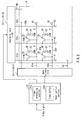
- FIG. 2 is a view illustrating a configuration of the active matrix substrate and main portions of the liquid crystal display device according to the first embodiment.
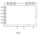
- FIG. 3 is a view illustrating a specific configuration of the active matrix substrate.
- the liquid crystal display device 1 ( FIG. 1 ) includes a panel control portion 22 that controls the driving of the liquid crystal panel 2 ( FIG. 1 ) as a display portion for displaying information such as characters and images, and a plurality of (for example, ten) source drivers 23-1, 23-2, ..., 23-9, and 23-10 (hereinafter, collectively referred to as "23") and a plurality of (for example, six) gate drivers 24-1, 24-2, ..., 24-5, and 24-6 (hereinafter, collectively referred to as "24") that are operated based on instruction signals from the panel control portion 22.
- a panel control portion 22 that controls the driving of the liquid crystal panel 2 ( FIG. 1 ) as a display portion for displaying information such as characters and images
- a plurality of (for example, ten) source drivers 23-1, 23-2, ..., 23-9, and 23-10 hereinafter, collectively referred to as "23”
- gate drivers 24-1, 24-2, ..., 24-5, and 24-6 hereinafter, collectively
- the panel control portion 22 is provided in the drive circuit device 10 ( FIG. 1 ) and receives a video signal from the outside of the liquid crystal display device 1. Further, the panel control portion 22 includes an image processing portion 22a that performs predetermined image processing on the input video signal and generates the instruction signals respectively for the source drivers 23 and the gate drivers 24, and a frame buffer 22b that can store display data for one frame included in the input video signal. When the panel control portion 22 controls the driving of the source drivers 23 and the gate drivers 24 according to the input video signal, information in accordance with the video signal is displayed on the liquid crystal panel 2.
- the source drivers 23 and the gate drivers 24 are provided in the drive device 9 ( FIG. 1 ) and are located on the active matrix substrate 5 of the present embodiment that forms an array substrate. Specifically, on a surface of the active matrix substrate 5, the source drivers 23-1 to 23-10 are located linearly along a lateral direction of the liquid crystal panel 2 in a region outside an effective display region A of the liquid crystal panel 2 as a display panel. Further, on the surface of the active matrix substrate 5, the gate drivers 24-1 to 24-6 are located linearly along a longitudinal direction (scanning direction to be described later) of the liquid crystal panel 2 in a region outside the effective display region A.
- the source drivers 23 and the gate drivers 24 serve as drive circuits for driving a plurality of pixels P provided in the liquid crystal panel 2 on a pixel basis and are connected with a plurality of source wirings S 1 to SM (M is an integer of 10 or more; hereinafter, collectively referred to as "S") and a plurality of gate wirings G1 to GN (N is an integer of 6 or more; hereinafter, collectively referred to as "N”), respectively.
- S 1 to SM M is an integer of 10 or more; hereinafter, collectively referred to as "S”
- N is an integer of 6 or more; hereinafter, collectively referred to as "N"
- each of the source drivers 23-1 to 23-10 is connected with the (M/10) source wirings S each of which functions as a data wiring to which a voltage signal in accordance with the video signal is input from the source driver 23.
- each of the gate drivers 24-1 to 24-6 is connected with the (N/6) gate wirings G each of which functions as a scanning wiring to which scanning signals are input sequentially from the gate driver 24 as a scanning wiring drive circuit, so that a scanning operation is performed.
- the number of a terminal that is corrected to the gate wiring G and the number of a vacant terminal that is not connected to the gate wiring G, as shown in FIG. 3 without hatching and with hatching, respectively are set to be 1/2 of the number of the entire terminals (details will be described later).
- the source wirings S and the gate wirings G are arranged in a matrix at least in the effective display region A, and regions of a plurality of the pixels P are formed in respective areas partitioned in a matrix.
- the source wirings S include source wiring main body portions S1b, S2b, S3b, and ... that are arranged in parallel with the longitudinal direction of the liquid crystal panel 2, and connection wiring portions S1a, S2a, S3a, and ... that respectively connect the source wiring main body portions S1b, S2b, S3b, and ... and the corresponding source drivers 23-1 to 23-10 in the shortest possible distances.
- the gate wirings G include gate wiring main body portions G1b, G2b, and ... that are arranged in parallel with the lateral direction of the liquid crystal panel 2, and connection wiring portions G1a, G2a, and ... that respectively connect the gate wiring main body portions G1b, G2b, and ... and the corresponding gate drivers 24-1 to 24-6 in the shortest possible distances.
- the source wiring main body portions S1b, S2b, S3b, and ... and the gate wiring main body portions G1b, G2b, and ... are arranged in a matrix. Since the connection wiring portions S1a, S2a, S3a, and ... connect the source wiring main body portions S1b, S2b, S3b, and ... and the corresponding source drivers 23-1 to 23-10 in the shortest possible distances, the connection wiring portions S1a, S2a, S3a, and ... have the smallest possible resistance value. Similarly, since the connection wiring portions G1a, G2a, and ... connect the gate wiring main body portions G1b, G2b, and ... and the corresponding gate drivers 24-1 to 24-6 in the shortest possible distances, the connection wiring portions G1a, G2a, and ... have the smallest possible resistance value.
- a plurality of the pixels P include red, green, and blue pixels.
- the red, green, and blue pixels are provided sequentially in this order, for example, in parallel with the gate wiring main body portions G1b, G2b, and ... of the gate wirings G.
- each of the gate wiring main body portions G1a, G2a, and ... is connected with a gate of a switching element 25 that is provided for each of the pixels P.
- each of the source wiring main body portions S1b, S2b, S3b, and ... is connected with a source of the switching element 25.
- a drain of the switching element 25 is connected with a pixel electrode 26 that is provided for each of the pixels P.
- a common electrode 27 is formed so as to be opposed to the pixel electrode 26 with the liquid crystal layer 4 ( FIG. 1 ) of the liquid crystal panel 2 sandwiched therebetween.
- the gate drivers 24 Based on the instruction signals from the image processing portion 22a, the gate drivers 24 sequentially output scanning signals to the gate wirings G1 to GN so as to turn on the gates of the corresponding switching elements 25.
- the source drivers 23 output the voltage signal (gray-scale voltage) in accordance with the brightness (gray-scale) of a display image to the corresponding source wirings S1 to SM based on the instruction signals from the image processing portion 22a.
- FIG. 4 is a block diagram showing a specific configuration of each of the gate drivers shown in FIG. 3 .
- each of the gate drivers 24 includes a control logic 24a to which the instruction signal from the image processing portion 22a ( FIG. 2 ) is input, a two-way register 24b and a level shifter 24c that are connected to the control logic 24a, and an output circuit 24d that has a plurality of (for example, X (X is an integer of 2 or more)) terminals OG1, OG2, ..., and OGx for outputting the scanning signals and is connected to the level shifter 24c.
- X is an integer of 2 or more
- the control logic 24a receives a vertical shift clock signal GCK and an output enable signal GOE from the image processing portion 22a. Further, the control logic 24a is supplied with a high-level side power supply voltage VCC and a low-level side power supply voltage GND for the logic, and generates a control signal required for driving the two-way register 24b based on the instruction signal from the image processing portion 22a, thereby operating the two-way register 24b.
- the two-way register 24b outputs a start signal to the level shifter 24c so as to start outputting the scanning signals through the control logic 24a. Further, the two-way register 24b sequentially outputs the scanning signals to the level shifter 24c.
- the level shifter 24c is supplied with a high-level side power supply voltage VGH and a low-level side power supply voltage VGL for driving liquid crystal. Further, when receiving the start signal followed by the scanning signals sequentially from the two-way register 24b, the level shifter 24c shifts the level of the scanning signals between a high level and a low level sequentially, and sequentially outputs the scanning signals to the output circuit 24d. Thus, the level shifter 24c allows the scanning signals to be output from the output circuit 24d in predetermined scanning directions.
- the output circuit 24d only X/2 of the X terminals OG1, OG2, ..., and OGx are connected to the gate wirings G as shown in FIG. 3 without hatching and with hatching.
- the output circuit 24d only the terminals OG1 to OG(x/2) provided on the upper side in FIG. 3 are connected to the gate wirings G, and the terminals OG(x/2 + 1) to OGx provided on the lower side in FIG. 3 are not connected to the gate wirings G as vacant terminals.
- the output circuit 24d sequentially outputs the scanning signals in the order from the terminal OG1 to the terminal OGx (i.e., in a scanning direction from the upper side to the lower side in FIG. 3 ).
- the six gate drivers 24-1 to 24-6 are configured to output the scanning signals sequentially in the order in which they are provided along the scanning direction from the upper side to the lower side in FIG. 3 , which will be described in detail later.
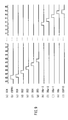
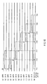
- FIG. 5 is a timing chart showing a scanning operation in the active matrix substrate.
- the gate driver 24-1 starts outputting the scanning signals sequentially from the terminal OG1 at a time point T1 and outputs the scanning signal from the terminal OG(x/2) at a time point T2 as indicated by (b) in FIG. 5 . Then, when the scanning signals are output completely from the terminals OG1 to OG(x/2) connected to the gate wirings G, a scanning operation is performed in a display region including the gate wirings G connected to the gate driver 24-1 between the time point T1 and the time point T2 as indicated by (m) in FIG. 5 .
- the scanning signals are output to the vacant terminals OG(x/2 + 1) to OGx.
- these vacant terminals OG(x/2 + 1) to OGx are not connected to the gate wirings G, they do not contribute to a display operation on the liquid crystal panel 2 (the same applies to the gate drivers 24-2 to 24-6).
- the gate driver 24-2 starts outputting the scanning signals sequentially from the terminal OG1 at the time point T2 and outputs the scanning signal from the terminal OG(x/2) at the time point T3 as indicated by (d) in FIG. 5 .
- the scanning signals are output completely from the terminals OG1 to OG(x/2) connected to the gate wirings G, a scanning operation is performed in a display region including the gate wirings G connected to the gate driver 24-2 between the time point T2 and the time point T3 as indicated by (m) in FIG. 5 .
- the gate driver 24-3 starts outputting the scanning signals sequentially from the terminal OG1 at the time point T3 and outputs the scanning signal from the terminal OG(x/2) at a time point T4 as indicated by (f) in FIG. 5 .
- the scanning signals are output completely from the terminals OG1 to OG(x/2) connected to the gate wirings G, a scanning operation is performed in a display region including the gate wirings G connected to the gate driver 24-3 between the time point T3 and the time point T4 as indicated by (m) in FIG. 5 .
- the gate driver 24-4 starts outputting the scanning signals sequentially from the terminal OG1 at the time point T4 and outputs the scanning signal from the terminal OG(x/2) at a time point T5 as indicated by (h) in FIG. 5 .
- the scanning signals are output completely from the terminals OG1 to OG(x/2) connected to the gate wirings G, a scanning operation is performed in a display region including the gate wirings G connected to the gate driver 24-4 between the time point T4 and the time point T5 as indicated by (m) in FIG. 5 .
- the gate driver 24-5 starts outputting the scanning signals sequentially from the terminal OG1 at the time point T5 and outputs the scanning signal from the terminal OG(x/2) at a time point T6 as indicated by (j) in FIG. 5 .
- the scanning signals are output completely from the terminals OG1 to OG(x/2) connected to the gate wirings G, a scanning operation is performed in a display region including the gate wirings G connected to the gate driver 24-5 between the time point T5 and the time point T6 as indicated by (m) in FIG. 5 .
- the gate driver 24-6 starts outputting the scanning signals sequentially from the terminal OG1 at the time point T6 and outputs the scanning signal from the terminal OG(x/2) at a time point T7 as indicated by (l) in FIG. 5 .
- the scanning signals are output completely from the terminals OG1 to OG(x/2) connected to the gate wirings G, a scanning operation is performed in a display region including the gate wirings G connected to the gate driver 24-6 between the time point T6 and the time point T7 as indicated by (m) in FIG. 5 . Consequently, one scanning operation on the entire liquid crystal panel 2 is completed.
- each of the gate drivers 24-1 to 24-6 is provided linearly along the scanning direction. Further, each of the gate drivers 24-1 to 24-6 includes the vacant terminals that are not connected to the gate wirings (scanning wirings) G1 to GN.
- the active matrix substrate 5 of the present embodiment even when the panel is made larger, it is possible to suppress an increase in the resistance value of the connection wirings (connection wiring portions G1a, G2a, ...) that connect the scanning wiring drive circuits (gate drivers 24) and the scanning wirings (gate wiring main body portions G1b, Gb2, ...), unlike the conventional example. Consequently, in the present embodiment, it is possible to configure easily the active matrix substrate 5 that enables a suitable scanning operation even when the panel is made larger, unlike the conventional example.
- the present embodiment uses the six gate drivers in each of which only X/2 of the X terminals OG1, OG2, ..., and OGx are connected to the gate wirings G, while the conventional example uses the three gate drivers in each of which all the X terminals are connected to the gate wirings.
- a maximum length of the scanning wirings is 1/3 of the length of the active matrix substrate in a vertical direction.
- a maximum length of the scanning wirings is 1/6 of the length of the active matrix substrate in a vertical direction.
- connection wirings connection wiring portions G1a, G2a, ...) that connect the scanning wiring drive circuits (gate drivers 24) and the scanning wirings (gate wiring main body portions G1b, G2b, ).
- the active matrix substrate 5 that enables a suitable scanning operation even when the panel is made larger is used in the liquid crystal panel (display portion) 2.
- the liquid crystal display device 1 that has excellent display performance even in the case of achieving a larger screen and/or higher definition.
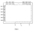
- FIG. 6 is a view illustrating a specific configuration of an active matrix substrate according to a second embodiment of the present invention.
- the present embodiment is different from the first embodiment mainly in that the terminal that is connected to gate wiring and the vacant terminal that is not connected to the gate wiring are provided sequentially in this order along a scanning direction in a gate driver provided on one end side of the scanning direction, while the vacant terminal that is not connected to the gate wiring and the terminal that is connected to the gate wiring are provided sequentially in this order along the scanning direction in a gate driver provided on the other end side of the scanning direction.
- the same elements as those in the first embodiment are denoted with the same reference numerals, and the repeated description thereof will be omitted.
- gate drivers 34-1 to 34-6 are located linearly along a longitudinal direction (scanning direction) of the liquid crystal panel 2 in a region outside the effective display region A.
- Each of the gate drivers 34-1 to 34-6 is connected with an equal number of the gate wirings G as in the first embodiment.
- the number of the terminal that is corrected to the gate wiring G and the number of the vacant terminal that is not connected to the gate wiring G, as shown in FIG. 6 without hatching and with hatching, respectively are set to be 1/2 of the number of the entire terminals.
- the active matrix substrate 5 of the present embodiment as shown in FIG. 6 as an example, in the gate drivers 34-1 and 34-6 that are provided respectively on the upper side (the one end side of the scanning direction) and the lower side (the other end side of the scanning direction) in FIG. 6 , the terminal that is connected to the gate wiring G and the vacant terminal that is not connected to the gate wiring G are located at positions different from each other. Consequently, according to the active matrix substrate 5 of the present embodiment, the scanning direction during a scanning operation by the gate drivers 34 can be reversed easily (details will be described later).
- FIG. 7 is a block diagram showing a specific configuration of each of the gate drivers shown in FIG. 6 .
- each of the gate drivers 34 includes a control logic 34a to which an instruction signal from the image processing portion 22a ( FIG. 2 ) is input, a two-way register 34b and a level shifter 34c that are connected to the control logic 34a, and an output circuit 34d that has X (X is an integer of 2 or more) terminals OG1, OG2, ..., and OGx for outputting scanning signals and is connected to the level shifter 34c, as in the first embodiment.
- only the gate drivers 34-6 includes the vacant terminal that is not connected to the gate wiring G and the terminal that is connected to the gate wiring G in this order.
- the gate drivers 34-1 to 34-5 among the terminals OG1 to OGx provided in the output circuit 34d, only the terminals OG-1 to OG(x/2) provided on the upper side in FIG. 6 are connected to the gate wirings G, and the terminals OG(x/2 + 1) to OGx provided on the lower side in FIG. 6 are not connected to the gate wirings G as vacant terminals as in the first embodiment.
- the terminals OG1 to OG(x/2) provided on the upper side in FIG. 6 are not connected to the gate wirings G as vacant terminals, and only the terminals OG(x/2 + 1) to OGx provided on the lower side in FIG. 6 are connected to the gate wirings G.
- the gate drivers 34 are configured so that the scanning direction during a scanning operation can be reversed.
- the control logic 34a includes a terminal for switching the scanning direction. That is, the control logic 34a receives from the image processing portion 22a a switching signal LBR that instructs the control logic 34a to switch between a scanning operation that is performed in a scanning direction from the upper side to the lower side in FIG. 6 (hereinafter, referred to as "normal scanning") and a scanning operation that is performed in a scanning direction from the lower side to the upper side in FIG. 6 (hereinafter, referred to as "reverse scanning"). More specifically, when the switching signal LBR is at a low level/high level, each of the gate drivers 34 performs normal scanning/reverse scanning.
- the control logic 34a includes input/output terminals GSPOI and GSPIO for inputting/outputting a control signal that makes a notification that the scanning signals are started to be output. More specifically, when normal scanning is performed, each of the gate drivers 34 outputs through the input/output terminal GSPIO the control signal that notifies the subsequent gate driver 34 in the scanning direction that the scanning signals are started to be output, and the subsequent gate driver 34 receives the control signal through the input/output terminal GSPOI. When reverse scanning is performed, the control signal that makes a notification that the scanning signals are started to be output is input/output with the input/output terminals GSPOI and GSPIO functioning in reverse manners to how they function in normal scanning.
- FIG. 8 is a timing chart showing a specific example of a scanning operation in the active matrix substrate shown in FIG. 6 .
- FIG. 9 is a timing chart showing an example of an operation of the gate driver shown in FIG. 7 during the scanning operation shown in FIG. 8 .
- FIG. 10 is a timing chart showing another specific example of the scanning operation in the active matrix substrate shown in FIG. 6 .
- FIG. 11 is a timing chart showing an example of the operation of the gate driver shown in FIG. 7 during the scanning operation shown in FIG. 10 .
- the gate driver 34-1 starts outputting the scanning signals sequentially from the terminal OG1 at a time point T8 and outputs the scanning signal from the terminal OG(x/2) at a time point T9 as indicated by (b) in FIG. 8 . Then, when the scanning signals are output completely from the terminals OG1 to OG(x/2) connected to the gate wirings G, a scanning operation is performed in a display region including the gate wirings G connected to the gate driver 34-1 between the time point T8 and the time point T9 as indicated by (m) in FIG. 8 .
- the scanning signals are output to the vacant terminals OG(x/2 + 1) to OGx.
- these vacant terminals OG(x/2 + 1) to OGx are not connected to the gate wirings G, they do not contribute to a display operation on the liquid crystal panel 2 (the same applies to the gate drivers 34-2 to 34-5).
- the gate driver 34-2 starts outputting the scanning signals sequentially from the terminal OG1 at the time point T9 and outputs the scanning signal from the terminal OG(x/2) at the time point T3 as indicated by (d) in FIG. 8 .
- the scanning signals are output completely from the terminals OG1 to OG(x/2) connected to the gate wirings G, a scanning operation is performed in a display region including the gate wirings G connected to the gate driver 34-2 between the time point T9 and the time point T10 as indicated by (m) in FIG. 8 .
- the gate driver 34-2 When the gate driver 34-2 receives the control signal from the gate driver 34-1 through the input/output terminal GSPOI as indicated by (b) in FIG. 9 , the scanning signals are output sequentially from the terminals OG1 to OGx as indicated respectively by (c) to (k) in FIG. 9 in synchronization with the vertical shift clock signal GCK as indicated by (a) in FIG. 9 . Further, the gate driver 34-2 outputs the control signal through the input/output terminal GSPIO to the gate driver 34-3 in synchronization with the output of the scanning signal from the terminal OGx. As a result, the gate driver 34-3 is notified that the scanning signals are started to be output from the gate driver 34-2.
- the gate driver 34-3 starts outputting the scanning signals sequentially from the terminal OG1 at the time point T10 and outputs the scanning signal from the terminal OG(x/2) at a time point T11 as indicated by (f) in FIG. 8 .
- the gate driver 34-4 starts outputting the scanning signals sequentially from the terminal OG1 at the time point T11 and outputs the scanning signal from the terminal OG(x/2) at a time point T12 as indicated by (h) in FIG. 8 .
- the scanning signals are output completely from the terminals OG1 to OG(x/2) connected to the gate wirings G, a scanning operation is performed in a display region including the gate wirings G connected to the gate driver 34-4 between the time point T11 and the time point T12 as indicated by (m) in FIG. 8 .
- the gate driver 34-5 starts outputting the scanning signals sequentially from the terminal OG1 at the time point T12 and outputs the scanning signal from the terminal OG(x/2) at a time point T13 as indicated by (j) in FIG. 8 .
- the scanning signals are output completely from the terminals OG1 to OG(x/2) connected to the gate wirings G, a scanning operation is performed in a display region including the gate wirings G connected to the gate driver 34-5 between the time point T12 and the time point T13 as indicated by (m) in FIG. 8 .
- the terminals OG1 to OG(x/2) provided on the upper side in FIG. 6 are vacant terminals.
- the image processing portion 22a outputs the instruction signal GSP6 that instructs the gate driver 34-6 to start a scanning operation just before the time point T12 as indicated by (k) in FIG. 8 .
- the image processing portion 22a outputs the instruction signals GSP5 and GSP6 at the same timing.
- the scanning signals are output to the vacant terminals OG1 to OG(x/2).
- these vacant terminals OG1 to OG(x/2) are not connected to the gate wirings G, they do not contribute to a display operation on the liquid crystal panel 2.
- the gate driver 34-6 starts outputting the scanning signals sequentially from the terminal OG(x/2 + 1) at the time point T6 and outputs the scanning signal from the terminal OGx at a time point T14 as indicated by (l) in FIG. 8 .
- the scanning signals are output completely from the terminals OG(x/2 + 1) to OGx connected to the gate wirings G
- a scanning operation is performed in a display region including the gate wirings G connected to the gate driver 34-6 between the time point T13 and the time point T14 as indicated by (m) in FIG. 8 . Consequently, one scanning operation on the entire liquid crystal panel 2 is completed.
- the gate driver 34-6 starts outputting the scanning signals sequentially from the terminal OGx at a time point T15 and outputs the scanning signal from the terminal OG(x/2 + 1) at a time point T16 as indicated by (b) in FIG. 10 . Then, when the scanning signals are output completely from the terminals OGx to OG(x/2 + 1) connected to the gate wirings G, a scanning operation is performed in a display region including the gate wirings G connected to the gate driver 34-6 between the time point T15 and the time point T16 as indicated by (m) in FIG. 10 .
- the scanning signals are output to the vacant terminals OG(x/2) to OG1.
- these vacant terminals OG(x/2) to OG1 are not connected to the gate wirings G, they do not contribute to a display operation on the liquid crystal panel 2.
- the terminals OG(x/2 + 1) to OGx provided on the lower side in FIG. 6 are vacant terminals.
- the image processing portion 22a outputs the instruction signal GSP5 that instructs the gate driver 34-5 to start a scanning operation just before the time point T15 as indicated by (c) in FIG. 10 .
- the image processing portion 22a outputs the instruction signals GSP5 and GSP6 at the same timing.
- the scanning signals are output to the vacant terminals OG(x/2 + 1) to OGx.
- these vacant terminals OG(x/2 + 1) to OGx are not connected to the gate wirings G, they do not contribute to a display operation on the liquid crystal panel 2 (the same applies to the gate drivers 34-2 to 34-5).
- the gate driver 34-5 starts outputting the scanning signals sequentially from the terminal OG(x/2) at the time point T16 and outputs the scanning signal from the terminal OG1 at the time point T17 as indicated by (d) in FIG. 10 .
- the scanning signals are output completely from the terminals OG(x/2) to OG1 connected to the gate wirings G, a scanning operation is performed in a display region including the gate wirings G connected to the gate driver 34-5 between the time point T16 and the time point T17 as indicated by (m) in FIG. 10 .
- the gate driver 34-5 When the gate driver 34-5 receives the control signal from the gate driver 34-6 through the input/output terminal GSPIO as indicated by (b) in FIG. 11 , the scanning signals are output sequentially from the terminals OGx to OG1 as indicated respectively by (c) to (k) in FIG. 11 in synchronization with the vertical shift clock signal GCK as indicated by (a) in FIG. 11 . Further, the gate driver 34-5 outputs the control signal through the input/output terminal GSPOI to the gate driver 34-4 in synchronization with the output of the scanning signal from the terminal OG1. As a result, the gate driver 34-4 is notified that the scanning signals are started to be output from the gate driver 34-5.
- the gate driver 34-4 starts outputting the scanning signals sequentially from the terminal OG(x/2) at the time point T17 and outputs the scanning signal from the terminal OG1 at a time point T18 as indicated by (f) in FIG. 10 .
- the gate driver 34-3 starts outputting the scanning signals sequentially from the terminal OG(x/2) at the time point T18 and outputs the scanning signal from the terminal OG1 at a time point T19 as indicated by (h) in FIG. 10 .
- the scanning signals are output completely from the terminals OG(x/2) to OG1 connected to the gate wirings G, a scanning operation is performed in a display region including the gate wirings G connected to the gate driver 34-3 between the time point T18 and the time point T19 as indicated by (m) in FIG. 10 .
- the gate driver 34-2 starts outputting the scanning signals sequentially from the terminal OG(x/2) at the time point T19 and outputs the scanning signal from the terminal OG1 at a time point T20 as indicated by (j) in FIG. 10 .
- the scanning signals are output completely from the terminals OG(x/2) to OG1 connected to the gate wirings G, a scanning operation is performed in a display region including the gate wirings G connected to the gate driver 34-2 between the time point T19 and the time point T20 as indicated by (m) in FIG. 10 .
- the gate driver 34-1 starts outputting the scanning signals sequentially from the terminal OG(x/2) at the time point T20 and outputs the scanning signal from the terminal OG1 at a time point T21 as indicated by (l) in FIG. 10 .
- the scanning signals are output completely from the terminals OG(x/2) to OG1 connected to the gate wirings G, a scanning operation is performed in a display region including the gate wirings G connected to the gate driver 34-1 between the time point T20 and the time point T21 as indicated by (m) in FIG. 10 . Consequently, one scanning operation on the entire liquid crystal panel 2 is completed.
- the present embodiment can provide the same function and achieve the same effect as those in the first embodiment. Further, the active matrix substrate 5 of the present embodiment enables normal scanning and reverse scanning suitably as shown in FIGs. 8 and 10 by reversing the scanning direction easily. As a result, with the active matrix substrate 5 of the present embodiment, it is possible to perform upside-down driving easily. On the other hand, with the active matrix substrate 5 of the first embodiment, it is not easy to perform suitable reverse scanning.
- the image processing portion 22a is required to output the instruction signal GSP6 to the gate driver 24-6 before a period between a time point T23 and a time point T24 during which a scanning operation is performed in a display region including the gate wirings G connected to the gate driver 24-6 as indicated by (e) in FIG. 12 .
- the image processing portion 22a cannot grasp an exact timing of the time point T22, and thus it is not easy to perform suitable reverse scanning
- the display device of the present invention is not limited thereto, as long as a display panel provided with an active matrix substrate is used in a display portion.
- the display device of the present invention is not limited particularly, as long as it uses an active matrix substrate in which a plurality of data wirings and a plurality of scanning wirings are arranged in a matrix, and a plurality of pixels are provided in the vicinities of intersections of the data wirings and the scanning wirings.
- the display device of the present invention can be applied to various types of display devices using an active matrix substrate, such as a semi-transmission type or reflection type liquid crystal panel, an organic EL (Electronic Luminescence) element, an inorganic EL element, and a Field Emission Display.
- an active matrix substrate such as a semi-transmission type or reflection type liquid crystal panel, an organic EL (Electronic Luminescence) element, an inorganic EL element, and a Field Emission Display.
- the location, number, and the like of the scanning wiring drive circuits are not limited thereto, as long as a plurality of the scanning wiring drive circuits are provided along the scanning direction.
- the terminal that is connected to the gate wiring (scanning wiring) and the vacant terminal that is not connected to the gate wiring are provided sequentially in this order along a scanning direction in the gate driver (scanning wiring drive circuit) provided on one end side of the scanning direction, while the vacant terminal that is not connected to the gate wiring and the terminal that is connected to the gate wiring are provided sequentially in this order along the scanning direction in the gate driver provided on the other end side of the scanning direction.
- the present invention is not limited thereto, as long as among a plurality of the scanning wiring drive circuits, in the scanning wiring drive circuit provided on one end side of the scanning direction, the terminal that is connected to the scanning wiring is provided on either one of the one end side and the other end side of the scanning direction, while in the scanning wiring drive circuit provided on the other end side of the scanning direction, the terminal that is connected to the scanning wiring is provided on the other of the one end side and the other end side of the scanning direction.
- only the terminal on one endmost side may be a vacant terminal, and the terminal that is connected to the scanning wiring may be provided subsequently to the vacant terminal on the one end side.
- only the terminal on the other endmost side may be a vacant terminal, and the terminal that is connected to the scanning wiring may be provided subsequently to one end side of the vacant terminal on the other end side, while in the scanning wiring drive circuit provided on the other end side of the scanning direction, only the terminal on the one endmost side may be a vacant terminal, and the terminal that is connected to the scanning wiring may be provided subsequently to the other end side of the vacant terminal on the one end side.
- the configuration as in the second embodiment is preferred, because it makes it possible to reverse the scanning direction, so that upside-down driving in which a video is displayed upside down exactly can be performed more easily.
- the present invention is not limited thereto, as long as the vacant terminal that is not connected to the scanning wiring is provided in the scanning wiring drive circuit.
- each of a plurality of the scanning wiring drive circuits has an equal number of the terminal that is connected to the scanning wiring and an equal number of the vacant terminal that is not connected to the scanning wiring as in the above-described embodiments, because this allows all the scanning wiring drive circuits to be loaded uniformly and enables an easy scanning operation.
- each of the scanning wiring drive circuits has the terminal that is connected to the scanning wiring and the vacant terminal that is not connected to the scanning wiring in equal numbers as in the above-described embodiments, because this makes it possible to simplify the operation of connecting the scanning wiring drive circuit and the scanning wiring and enables an easier scanning operation.
- the present invention is useful for an active matrix substrate that enables a suitable scanning operation even when a panel is made larger, and a high-performance display device using the same.
Landscapes
- Engineering & Computer Science (AREA)
- Chemical & Material Sciences (AREA)
- Crystallography & Structural Chemistry (AREA)
- Physics & Mathematics (AREA)
- Computer Hardware Design (AREA)
- General Physics & Mathematics (AREA)
- Theoretical Computer Science (AREA)
- Control Of Indicators Other Than Cathode Ray Tubes (AREA)
- Liquid Crystal (AREA)
- Liquid Crystal Display Device Control (AREA)
- Devices For Indicating Variable Information By Combining Individual Elements (AREA)
Abstract
Description
- The present invention relates to an active matrix substrate in which a plurality of data wirings and a plurality of scanning wirings are arranged in a matrix, and a display device using the same.
- Recently, for example, a liquid crystal display device has been used widely in a liquid crystal television, a monitor, a mobile phone, and the like as a flat panel display having features such as thinness and a light weight as compared with a conventional Broun tube. A known liquid crystal display device of this kind uses, in a liquid crystal panel as a display panel, an active matrix substrate in which a plurality of data wirings and a plurality of scanning wirings are arranged in a matrix, and pixels, each having a switching element such as a TFT (Thin Film Transistor), are arranged in a matrix in the vicinities of intersections of the data wirings and the scanning wirings (for example, see
JP 2003-58119 A - Further, as described in
JP 2006-337710 A - Further, in the conventional active matrix substrate, the gate drivers on the both sides are connected to each other via the scanning wirings. This prevents an increase in circuit scale even when the gate drivers are provided on the both sides of the display portion, making it possible to provide a smaller liquid crystal display device.
- However, in the conventional active matrix substrate as described above, the scanning operation by the gate drivers (scanning wiring drive circuits) may not be performed suitably in the case where the panel is made larger (including the case where the number of the pixels is increased) for the purpose of achieving a larger-screen and higher-definition liquid crystal display device, for example.
- Specifically, in the conventional active matrix substrate, when the number of the scanning wirings is increased with an increased number of the pixels, or when the panel is made larger for the purpose of achieving a larger screen, it becomes necessary to make a connection wiring, which connects each of the gate drivers on the both sides and each of the scanning wirings, finer or longer, and it may cause a significant increase in the resistance value of the connection wiring. More specifically, in the conventional active matrix substrate, when the panel is made larger, a distance between the scanning wirings provided on one end side in a scanning direction (for example, a row direction of the matrix) and the scanning wirings provided on the other end side increases significantly, relative to the dimension of the gate drivers in the scanning direction. As a result, in the conventional active matrix substrate, for example, the connection wiring that connects each of the scanning wirings provided on the one end side and each of the gate drivers becomes longer, resulting in an increase in the resistance value of the connection wiring.
- Further, an increase in the number of the scanning wirings to be connected to each of the gate drivers makes it necessary to narrow a space (pitch) between the adjacent two connection wirings and hence to reduce a width dimension (cross sectional area) of a plurality of the connection wirings to be connected respectively to a plurality of the scanning wirings. In other words, in the conventional active matrix substrate, it is necessary to make a plurality of the entire connection wirings finer in accordance with an increase in the number of the pixels, which may result in a significant increase in the resistance value of the connection wirings. As a result, in the conventional active matrix substrate, the scanning signals may be reduced significantly depending on the distance from each of the gate drivers, which may make it impossible to perform a suitable scanning operation.
- In order to address an increase in the resistance value as described above, a voltage value of the scanning signals from each of the gate drivers may be increased. However, this necessitates a significant increase in the cost each of the gate drivers and an unnecessary increase in the dielectric strength each of the connection wirings, the scanning wirings, and the like. Thus, another problem may arise in that the active matrix substrate may be made more complicated and larger.
- In view of the above-described problems, it is an object of the present invention to provide an active matrix substrate that enables a suitable scanning operation even when a panel is made larger, and a display device using the same.
- In order to achieve the above-described object, an active matrix substrate according to the present invention is for use as a substrate of a display panel. The substrate includes a plurality of data wirings and a plurality of scanning wirings arranged in a matrix and a plurality of pixels provided in the vicinities of intersections of the data wirings and the scanning wirings. A plurality of scanning wiring drive circuits that sequentially output scanning signals to a plurality of the scanning wirings in a predetermined scanning direction are provided along the scanning direction, and each of a plurality of the scanning wiring drive circuits has a vacant terminal that is not connected to the scanning wiring.
- According to the active matrix substrate configured as described above, a plurality of the scanning wiring drive circuits are provided along the scanning direction. Further, each of a plurality of the scanning wiring drive circuits has the vacant terminal that is not connected to the scanning wiring. Therefore, unlike the conventional example, even when a panel is made larger, it is possible to suppress an increase in the resistance value of a connection wiring that connects the scanning wiring drive circuit and the scanning wiring. Consequently, unlike the conventional example, it is possible to configure easily the active matrix substrate that enables a suitable scanning operation even when a panel is made larger.
- Further, in the above-described active matrix substrate, among a plurality of the scanning wiring drive circuits, in the scanning wiring drive circuit provided on one end side of the scanning direction, a terminal that is connected to the scanning wiring may be provided on either one of the one end side and the other end side of the scanning direction, and in the scanning wiring drive circuit provided on the other end side of the scanning direction, a terminal that is connected to the scanning wiring may be provided on the other of the one end side and the other end side of the scanning direction.
- In this case, it is possible to reverse the scanning direction, so that upside-down driving in which a video is displayed upside down exactly can be performed easily.
- Further, in the above-described active matrix substrate, among a plurality of the scanning wiring drive circuits, in the scanning wiring drive circuit provided on the one end side of the scanning direction, the terminal that is connected to the scanning wiring and the vacant terminal that is not connected to the scanning wiring preferably are provided sequentially in this order along the scanning direction, and in the scanning wiring drive circuit provided on the other end side of the scanning direction, the vacant terminal that is not connected to the scanning wiring and the terminal that is connected to the scanning wiring preferably are provided sequentially in this order along the scanning direction.
- In this case, it is possible to reverse the scanning direction, so that upside-down driving in which a video is displayed upside down exactly can be performed more easily.
- Further, in the above-described active matrix substrate, each of a plurality of the scanning wiring drive circuits preferably has an equal number of the terminal that is connected to the scanning wiring and an equal number of the vacant terminal that is not connected to the scanning wiring.
- This allows all the scanning wiring drive circuits to be loaded uniformly and enables an easy scanning operation.
- Further, in the above-described active matrix substrate, each of a plurality of the scanning wiring drive circuits may have the terminal that is connected to the scanning wiring and the vacant terminal that is not connected to the scanning wiring in equal numbers.
- This makes it possible to simplify the operation of connecting the scanning wiring drive circuit and the scanning wiring and enables an easier scanning operation.
- Further, a display device according to the present invention is provided with a display portion. The active matrix substrate according to any one of the above-described configurations is used in the display portion.
- In the display device configured as described above, the active matrix substrate that enables a suitable scanning operation even when a panel is made larger is used in the display portion. Thus, it is possible to configure easily the display device that has excellent display performance even in the case of achieving a larger screen and/or higher definition.
- According to the present invention, it is possible to provide an active matrix substrate that enables a suitable scanning operation even when a panel is made larger, and a display device using the same.
-
- [
FIG. 1] FIG. 1 is a schematic cross-sectional view illustrating a liquid crystal display device according to a first embodiment of the present invention. - [
FIG. 2] FIG. 2 is a view illustrating a configuration of an active matrix substrate and main portions of the liquid crystal display device according to the first embodiment. - [
FIG. 3] FIG. 3 is a view illustrating a specific configuration of the active matrix substrate. - [
FIG. 4] FIG. 4 is a block diagram showing a specific configuration of a gate driver shown inFIG. 3 . - [
FIG. 5] FIG. 5 is a timing chart showing a scanning operation in the active matrix substrate. - [
FIG. 6] FIG. 6 is a view illustrating a specific configuration of an active matrix substrate according to a second embodiment of the present invention. - [
FIG. 7] FIG. 7 is a block diagram showing a specific configuration of a gate driver shown inFIG. 6 . - [
FIG. 8] FIG. 8 is a timing chart showing a specific example of a scanning operation in the active matrix substrate shown inFIG. 6 . - [
FIG. 9] FIG. 9 is a timing chart showing an example of an operation of the gate driver shown inFIG. 7 during the scanning operation shown inFIG. 8 . - [
FIG. 10] FIG. 10 is a timing chart showing another specific example of the scanning operation in the active matrix substrate shown inFIG. 6 . - [
FIG. 11] FIG. 11 is a timing chart showing an example of the operation of the gate driver shown inFIG. 7 during the scanning operation shown inFIG. 10 . - [
FIG. 12] FIG. 12 is a view illustrating a problem to be caused when the scanning operation shown inFIG. 10 is performed in the active matrix substrate shown inFIG. 3 . - Hereinafter, preferred embodiments of an active matrix substrate and a display device according to the present invention will be described with reference to the drawings. It should be noted that the following description is directed to the case where the present invention is applied to a transmission type liquid crystal display device by way of example. Further, the size and size ratio of the constituent members in each figure do not exactly reflect those of actual constituent members.
-
FIG. 1 is a schematic cross-sectional view illustrating a liquid crystal display device according to a first embodiment of the present invention. In the figure, a liquidcrystal display device 1 of the present embodiment includes aliquid crystal panel 2 as a display portion that is located with the upper side in the figure defined as a viewing side (display surface side), and anilluminating device 3 that is arranged on the non-display surface side of the liquid crystal panel 2 (lower side in the figure) and generates illumination light to illuminate theliquid crystal panel 2. - The
liquid crystal panel 2 includes aliquid crystal layer 4, anactive matrix substrate 5 of the present invention and acolor filter substrate 6 between which theliquid crystal layer 4 is sandwiched, and polarizingplates 7 and 8 provided respectively on outer surfaces of theactive matrix substrate 5 and thecolor filter substrate 6. Further, theliquid crystal panel 2 includes a driver device 9 for driving theliquid crystal panel 2, and adrive circuit device 10 connected to the driver device 9 via a flexible printedboard 11, so that theliquid crystal layer 4 can be driven on a pixel basis. In theliquid crystal panel 2, a polarization state of the illumination light incident through thepolarizing plate 7 is modulated by theliquid crystal layer 4, and an amount of light passing through the polarizing plate 8 is controlled, whereby a desired image is displayed. - It should be noted that the
liquid crystal panel 2 may be in any liquid crystal mode and have any pixel structure. Also, theliquid crystal panel 2 may be in any drive mode. In other words, theliquid crystal panel 2 may be any liquid crystal panel that can display information. Thus, a detailed structure of theliquid crystal panel 2 is not shown inFIG. 1 , and a description thereof will be omitted. - The illuminating
device 3 includes a bottomedchassis 12 with the upper side in the figure (liquid crystal panel 2 side) opened, and aframe 13 placed on theliquid crystal panel 2 side of thechassis 12. Further, thechassis 12 and theframe 13 are made of a metal or a synthetic resin and are sandwiched by abezel 14 having an L-shape in cross section with theliquid crystal panel 2 located above theframe 13. Thus, the illuminatingdevice 3 is assembled with theliquid crystal panel 2, so that they are integrated into the transmission type liquidcrystal display device 1 in which the illumination light from the illuminatingdevice 3 is incident on theliquid crystal panel 2. - Further, the illuminating
device 3 includes adiffusion plate 15 located so as to cover the opening of thechassis 12, anoptical sheet 17 located above thediffusion plate 15 on the liquid crystal penal 2 side, and a reflectingsheet 21 provided on an inner surface of thechassis 12. In the illuminatingdevice 3, a plurality of (for example, six) coldcathode fluorescent tubes 20 are provided inside thechassis 12 below theliquid crystal panel 2, thereby forming the directtype illuminating device 3. In the illuminatingdevice 3, light from the coldcathode fluorescent tubes 20 is output as the illumination light from a light-emitting surface of the illuminatingdevice 3 that is arranged so as to be opposed to theliquid crystal panel 2. - Although the above description is directed to the configuration using the direct
type illuminating device 3, the present embodiment is not limited thereto. Instead, an edge-light type illuminating device having a light guiding plate may be used. Further, an illuminating device having light sources other than the cold cathode fluorescent tubes, such as a hot cathode fluorescent tube and an LED, can be used. - The
diffusion plate 15, which is made of, for example, a rectangular-shaped synthetic resin or glass material having a thickness of about 2 mm, diffuses the light from the coldcathode fluorescent tubes 20 and outputs the light to theoptical sheet 17 side. Further, four sides of thediffusion plate 15 are placed on a frame-shaped surface of thechassis 12 provided on the upper side thereof, and thediffusion plate 15 is incorporated in the illuminatingdevice 3 while being sandwiched between the frame-shaped surface of thechassis 12 and an inner surface of theframe 13 with apressure member 16 capable of being deformed elastically interposed therebetween. Further, thediffusion plate 15 is supported substantially at its center by a transparent support member (not shown) located inside thechassis 12, whereby thediffusion plate 15 is prevented from being bent toward the inside of thechassis 12. - Further, the
diffusion plate 15 is held so as to be movable between thechassis 12 and thepressure member 16. Even when thediffusion plate 15 is expanded/contracted (deformed plastically) due to the influence of heat caused by heat generation in the coldcathode fluorescent tubes 20, temperature rise inside thechassis 12, and the like, the plastic deformation is absorbed by the elastic deformation of thepressure member 16, whereby a decrease in diffusion of the light from the coldcathode fluorescent tubes 20 is minimized. Further, it is preferred to use thediffusion plate 15 made of a glass material, which is more resistant to heat as compared with a synthetic resin, since warpage, yellowing, thermal deformation, and the like caused by the influence of heat are unlikely to occur. - The
optical sheet 17 includes a focusing sheet formed of, for example, a synthetic resin film having a thickness of about 0.5 mm and is configured to increase the brightness of the illumination light to theliquid crystal panel 2. Further, on theoptical sheet 17, known optical sheet materials such as a prism sheet, a diffusion sheet, and a polarizing sheet for enhancing the display quality on the display surface of theliquid crystal panel 2, for example, are laminated appropriately, if required. Theoptical sheet 17 is configured to convert the light output from thediffusion plate 15 into plane-shaped light having a predetermined brightness (for example, 10000 cd/m2) or more and having a uniform brightness and to allow the converted light to be incident on theliquid crystal panel 2 side as the illumination light. Besides the above description, for example, an optical member such as a diffusion sheet for adjusting the viewing angle of theliquid crystal panel 2 may be laminated appropriately above (on the display surface side of) theliquid crystal panel 2. - Further, the
optical sheet 17 is provided with a protrusion protruding to the left side in the figure at the center on the left end side inFIG. 1 , which is to be the upper side during actual use of the liquidcrystal display device 1, for example. In theoptical sheet 17, only the protrusion is sandwiched between the inner surface of theframe 13 and thepressure member 16 with anelastic material 18 interposed therebetween, and theoptical sheet 17 is incorporated in the illuminatingdevice 3 so as to be capable of expanding/contracting. Thus, theoptical sheet 17 is configured in such a manner that, even when the expansion/contraction (plastic) deformation occurs due to the influence of heat caused by heat generation in the coldcathode fluorescent tubes 20 and the like, theoptical sheet 17 is capable of expanding/contracting freely with respect to the protrusion, whereby wrinkles, warpage, and the like are minimized in theoptical sheet 17. Consequently, in the liquidcrystal display device 1, it is possible to minimize degradation in display quality such as non-uniform brightness on the display surface of theliquid crystal panel 2 due to warpage and the like of theoptical sheet 17. - Each of the cold
cathode fluorescent tubes 20 is of a straight-tube type, and electrode portions (not shown) provided at both ends thereof are supported outside thechassis 12. Also, each of the coldcathode fluorescent tubes 20 is configured to have a small diameter of about 3.0 to 4.0 mm so as to have excellent light-emission efficiency. The coldcathode fluorescent tubes 20 are held inside thechassis 12 while being kept at predetermined distances from thediffusion plate 15 and the reflectingsheet 21 by a light source holder not shown. Further, the coldcathode fluorescent tubes 20 are arranged so that a longitudinal direction thereof is parallel to a direction perpendicular to the direction of gravity. This arrangement prevents mercury (vapor) sealed inside each of the coldcathode fluorescent tubes 20 from being concentrated on one end side in the longitudinal direction due to the action of gravity, resulting in significantly improved lamp life. - The reflecting
sheet 21, which is formed of, for example, a thin metal film of aluminum, silver, or the like having a thickness of about 0.2 to 0.5 mm with a high light reflectance, functions as a reflector that reflects the light from the coldcathode fluorescent tubes 20 towards thediffusion plate 15. Thus, in the illuminatingdevice 3, the reflectingsheet 21 can reflect the light emitted from the coldcathode fluorescent tubes 20 to thediffusion plate 15 side efficiently so as to enhance the use efficiency of the light and the brightness in thediffusion plate 15. Besides the above description, instead of the thin metal film, a reflecting sheet material of a synthetic resin may be used, or alternatively, for example, a coating such as a white coating having a high light reflectance may be applied to the inner surface of thechassis 12 so that the inner surface functions as a reflector. - Next, the
active matrix substrate 5 of the present embodiment will be described specifically also with reference toFIGs. 2 and3 . -
FIG. 2 is a view illustrating a configuration of the active matrix substrate and main portions of the liquid crystal display device according to the first embodiment.
FIG. 3 is a view illustrating a specific configuration of the active matrix substrate. - In
FIGs. 2 and3 , the liquid crystal display device 1 (FIG. 1 ) includes apanel control portion 22 that controls the driving of the liquid crystal panel 2 (FIG. 1 ) as a display portion for displaying information such as characters and images, and a plurality of (for example, ten) source drivers 23-1, 23-2, ..., 23-9, and 23-10 (hereinafter, collectively referred to as "23") and a plurality of (for example, six) gate drivers 24-1, 24-2, ..., 24-5, and 24-6 (hereinafter, collectively referred to as "24") that are operated based on instruction signals from thepanel control portion 22. - The
panel control portion 22 is provided in the drive circuit device 10 (FIG. 1 ) and receives a video signal from the outside of the liquidcrystal display device 1. Further, thepanel control portion 22 includes animage processing portion 22a that performs predetermined image processing on the input video signal and generates the instruction signals respectively for the source drivers 23 and thegate drivers 24, and aframe buffer 22b that can store display data for one frame included in the input video signal. When thepanel control portion 22 controls the driving of the source drivers 23 and thegate drivers 24 according to the input video signal, information in accordance with the video signal is displayed on theliquid crystal panel 2. - The source drivers 23 and the
gate drivers 24 are provided in the drive device 9 (FIG. 1 ) and are located on theactive matrix substrate 5 of the present embodiment that forms an array substrate. Specifically, on a surface of theactive matrix substrate 5, the source drivers 23-1 to 23-10 are located linearly along a lateral direction of theliquid crystal panel 2 in a region outside an effective display region A of theliquid crystal panel 2 as a display panel. Further, on the surface of theactive matrix substrate 5, the gate drivers 24-1 to 24-6 are located linearly along a longitudinal direction (scanning direction to be described later) of theliquid crystal panel 2 in a region outside the effective display region A. - Further, the source drivers 23 and the
gate drivers 24 serve as drive circuits for driving a plurality of pixels P provided in theliquid crystal panel 2 on a pixel basis and are connected with a plurality ofsource wirings S 1 to SM (M is an integer of 10 or more; hereinafter, collectively referred to as "S") and a plurality of gate wirings G1 to GN (N is an integer of 6 or more; hereinafter, collectively referred to as "N"), respectively. Each of the source drivers 23-1 to 23-10 is connected with an equal number of the source wirings S, and each of the gate drivers 24-1 to 24-6 is connected with an equal number of the gate wirings G. - In other words, each of the source drivers 23-1 to 23-10 is connected with the (M/10) source wirings S each of which functions as a data wiring to which a voltage signal in accordance with the video signal is input from the source driver 23. Further, each of the gate drivers 24-1 to 24-6 is connected with the (N/6) gate wirings G each of which functions as a scanning wiring to which scanning signals are input sequentially from the
gate driver 24 as a scanning wiring drive circuit, so that a scanning operation is performed. - Further, in each of the gate drivers 24-1 to 24-6, the number of a terminal that is corrected to the gate wiring G and the number of a vacant terminal that is not connected to the gate wiring G, as shown in
FIG. 3 without hatching and with hatching, respectively are set to be 1/2 of the number of the entire terminals (details will be described later). - Further, the source wirings S and the gate wirings G are arranged in a matrix at least in the effective display region A, and regions of a plurality of the pixels P are formed in respective areas partitioned in a matrix. Specifically, as shown in
FIG. 2 as an example, the source wirings S include source wiring main body portions S1b, S2b, S3b, and ... that are arranged in parallel with the longitudinal direction of theliquid crystal panel 2, and connection wiring portions S1a, S2a, S3a, and ... that respectively connect the source wiring main body portions S1b, S2b, S3b, and ... and the corresponding source drivers 23-1 to 23-10 in the shortest possible distances. Similarly, the gate wirings G include gate wiring main body portions G1b, G2b, and ... that are arranged in parallel with the lateral direction of theliquid crystal panel 2, and connection wiring portions G1a, G2a, and ... that respectively connect the gate wiring main body portions G1b, G2b, and ... and the corresponding gate drivers 24-1 to 24-6 in the shortest possible distances. - In the source wirings S and the gate wirings G, the source wiring main body portions S1b, S2b, S3b, and ... and the gate wiring main body portions G1b, G2b, and ... are arranged in a matrix. Since the connection wiring portions S1a, S2a, S3a, and ... connect the source wiring main body portions S1b, S2b, S3b, and ... and the corresponding source drivers 23-1 to 23-10 in the shortest possible distances, the connection wiring portions S1a, S2a, S3a, and ... have the smallest possible resistance value. Similarly, since the connection wiring portions G1a, G2a, and ... connect the gate wiring main body portions G1b, G2b, and ... and the corresponding gate drivers 24-1 to 24-6 in the shortest possible distances, the connection wiring portions G1a, G2a, and ... have the smallest possible resistance value.
- A plurality of the pixels P include red, green, and blue pixels. The red, green, and blue pixels are provided sequentially in this order, for example, in parallel with the gate wiring main body portions G1b, G2b, and ... of the gate wirings G.
- Further, each of the gate wiring main body portions G1a, G2a, and ... is connected with a gate of a switching
element 25 that is provided for each of the pixels P. On the other hand, each of the source wiring main body portions S1b, S2b, S3b, and ... is connected with a source of the switchingelement 25. A drain of the switchingelement 25 is connected with apixel electrode 26 that is provided for each of the pixels P. In each of the pixels P, acommon electrode 27 is formed so as to be opposed to thepixel electrode 26 with the liquid crystal layer 4 (FIG. 1 ) of theliquid crystal panel 2 sandwiched therebetween. Based on the instruction signals from theimage processing portion 22a, thegate drivers 24 sequentially output scanning signals to the gate wirings G1 to GN so as to turn on the gates of thecorresponding switching elements 25. On the other hand, the source drivers 23 output the voltage signal (gray-scale voltage) in accordance with the brightness (gray-scale) of a display image to the corresponding source wirings S1 to SM based on the instruction signals from theimage processing portion 22a. - Next, the
gate drivers 24 of the present embodiment will be described specifically with reference toFIG. 4 . -
FIG. 4 is a block diagram showing a specific configuration of each of the gate drivers shown inFIG. 3 . - As shown in
FIG. 4 , each of thegate drivers 24 includes acontrol logic 24a to which the instruction signal from theimage processing portion 22a (FIG. 2 ) is input, a two-way register 24b and alevel shifter 24c that are connected to thecontrol logic 24a, and anoutput circuit 24d that has a plurality of (for example, X (X is an integer of 2 or more)) terminals OG1, OG2, ..., and OGx for outputting the scanning signals and is connected to thelevel shifter 24c. - The
control logic 24a receives a vertical shift clock signal GCK and an output enable signal GOE from theimage processing portion 22a. Further, thecontrol logic 24a is supplied with a high-level side power supply voltage VCC and a low-level side power supply voltage GND for the logic, and generates a control signal required for driving the two-way register 24b based on the instruction signal from theimage processing portion 22a, thereby operating the two-way register 24b. - In accordance with the control signal from the
control logic 24a, the two-way register 24b outputs a start signal to thelevel shifter 24c so as to start outputting the scanning signals through thecontrol logic 24a. Further, the two-way register 24b sequentially outputs the scanning signals to thelevel shifter 24c. - The
level shifter 24c is supplied with a high-level side power supply voltage VGH and a low-level side power supply voltage VGL for driving liquid crystal. Further, when receiving the start signal followed by the scanning signals sequentially from the two-way register 24b, thelevel shifter 24c shifts the level of the scanning signals between a high level and a low level sequentially, and sequentially outputs the scanning signals to theoutput circuit 24d. Thus, thelevel shifter 24c allows the scanning signals to be output from theoutput circuit 24d in predetermined scanning directions. - In the
output circuit 24d, only X/2 of the X terminals OG1, OG2, ..., and OGx are connected to the gate wirings G as shown inFIG. 3 without hatching and with hatching. In other words, in theoutput circuit 24d, only the terminals OG1 to OG(x/2) provided on the upper side inFIG. 3 are connected to the gate wirings G, and the terminals OG(x/2 + 1) to OGx provided on the lower side inFIG. 3 are not connected to the gate wirings G as vacant terminals. When receiving the start signal, theoutput circuit 24d sequentially outputs the scanning signals in the order from the terminal OG1 to the terminal OGx (i.e., in a scanning direction from the upper side to the lower side inFIG. 3 ). - Further, the six gate drivers 24-1 to 24-6 are configured to output the scanning signals sequentially in the order in which they are provided along the scanning direction from the upper side to the lower side in
FIG. 3 , which will be described in detail later. - An operation of the liquid
crystal display device 1 of the present embodiment configured as described above will be described specifically with reference toFIG. 5 .
It should be noted that the following description is directed mainly to a scanning operation by the gate drivers 24-1 to 24-6. -
FIG. 5 is a timing chart showing a scanning operation in the active matrix substrate. - When the
image processing portion 22a outputs an instruction signal GSP1 that instructs the top gate driver 24-1 to start a scanning operation as indicated by (a) inFIG. 5 , the gate driver 24-1 starts outputting the scanning signals sequentially from the terminal OG1 at a time point T1 and outputs the scanning signal from the terminal OG(x/2) at a time point T2 as indicated by (b) inFIG. 5 . Then, when the scanning signals are output completely from the terminals OG1 to OG(x/2) connected to the gate wirings G, a scanning operation is performed in a display region including the gate wirings G connected to the gate driver 24-1 between the time point T1 and the time point T2 as indicated by (m) inFIG. 5 . Further, in the gate driver 24-1, during a period between the time point T2 and a time point T3 (a hatched period in the figure), the scanning signals are output to the vacant terminals OG(x/2 + 1) to OGx. However, since these vacant terminals OG(x/2 + 1) to OGx are not connected to the gate wirings G, they do not contribute to a display operation on the liquid crystal panel 2 (the same applies to the gate drivers 24-2 to 24-6). - Next, when the
image processing portion 22a outputs an instruction signal GSP2 that instructs the second gate driver 24-2 from the top to start a scanning operation just before the time point T2 as indicated by (c) inFIG. 5 , the gate driver 24-2 starts outputting the scanning signals sequentially from the terminal OG1 at the time point T2 and outputs the scanning signal from the terminal OG(x/2) at the time point T3 as indicated by (d) inFIG. 5 . Then, when the scanning signals are output completely from the terminals OG1 to OG(x/2) connected to the gate wirings G, a scanning operation is performed in a display region including the gate wirings G connected to the gate driver 24-2 between the time point T2 and the time point T3 as indicated by (m) inFIG. 5 . - Then, when the
image processing portion 22a outputs an instruction signal GSP3 that instructs the third gate driver 24-3 from the top to start a scanning operation just before the time point T3 as indicated by (e) inFIG. 5 , the gate driver 24-3 starts outputting the scanning signals sequentially from the terminal OG1 at the time point T3 and outputs the scanning signal from the terminal OG(x/2) at a time point T4 as indicated by (f) inFIG. 5 . Then, when the scanning signals are output completely from the terminals OG1 to OG(x/2) connected to the gate wirings G, a scanning operation is performed in a display region including the gate wirings G connected to the gate driver 24-3 between the time point T3 and the time point T4 as indicated by (m) inFIG. 5 . - Thereafter, when the
image processing portion 22a outputs an instruction signal GSP4 that instructs the fourth gate driver 24-4 from the top to start a scanning operation just before the time point T4 as indicated by (g) inFIG. 5 , the gate driver 24-4 starts outputting the scanning signals sequentially from the terminal OG1 at the time point T4 and outputs the scanning signal from the terminal OG(x/2) at a time point T5 as indicated by (h) inFIG. 5 . Then, when the scanning signals are output completely from the terminals OG1 to OG(x/2) connected to the gate wirings G, a scanning operation is performed in a display region including the gate wirings G connected to the gate driver 24-4 between the time point T4 and the time point T5 as indicated by (m) inFIG. 5 . - Then, when the
image processing portion 22a outputs an instruction signal GSP5 that instructs the fifth gate driver 24-5 from the top to start a scanning operation just before the time point T5 as indicated by (i) inFIG. 5 , the gate driver 24-5 starts outputting the scanning signals sequentially from the terminal OG1 at the time point T5 and outputs the scanning signal from the terminal OG(x/2) at a time point T6 as indicated by (j) inFIG. 5 . Then, when the scanning signals are output completely from the terminals OG1 to OG(x/2) connected to the gate wirings G, a scanning operation is performed in a display region including the gate wirings G connected to the gate driver 24-5 between the time point T5 and the time point T6 as indicated by (m) inFIG. 5 . - After that, when the
image processing portion 22a outputs an instruction signal GSP6 that instructs the sixth gate driver 24-6 from the top to start a scanning operation just before the time point T6 as indicated by (k) inFIG. 5 , the gate driver 24-6 starts outputting the scanning signals sequentially from the terminal OG1 at the time point T6 and outputs the scanning signal from the terminal OG(x/2) at a time point T7 as indicated by (l) inFIG. 5 . Then, when the scanning signals are output completely from the terminals OG1 to OG(x/2) connected to the gate wirings G, a scanning operation is performed in a display region including the gate wirings G connected to the gate driver 24-6 between the time point T6 and the time point T7 as indicated by (m) inFIG. 5 . Consequently, one scanning operation on the entireliquid crystal panel 2 is completed. - In the
active matrix substrate 5 of the present embodiment configured as described above, the six gate drivers (scanning wiring drive circuits) 24-1 to 24-6 are provided linearly along the scanning direction. Further, each of the gate drivers 24-1 to 24-6 includes the vacant terminals that are not connected to the gate wirings (scanning wirings) G1 to GN. Thus, according to theactive matrix substrate 5 of the present embodiment, even when the panel is made larger, it is possible to suppress an increase in the resistance value of the connection wirings (connection wiring portions G1a, G2a, ...) that connect the scanning wiring drive circuits (gate drivers 24) and the scanning wirings (gate wiring main body portions G1b, Gb2, ...), unlike the conventional example. Consequently, in the present embodiment, it is possible to configure easily theactive matrix substrate 5 that enables a suitable scanning operation even when the panel is made larger, unlike the conventional example. - Namely, the present embodiment uses the six gate drivers in each of which only X/2 of the X terminals OG1, OG2, ..., and OGx are connected to the gate wirings G, while the conventional example uses the three gate drivers in each of which all the X terminals are connected to the gate wirings. In this case, in the conventional example, since the entire active matrix substrate is driven by the three gate drivers, a maximum length of the scanning wirings is 1/3 of the length of the active matrix substrate in a vertical direction. On the other hand, in the present embodiment, since the entire active matrix substrate is driven by the six gate drivers, a maximum length of the scanning wirings is 1/6 of the length of the active matrix substrate in a vertical direction. Thus, as compared with the conventional example, it is possible to suppress by half the resistance value of the connection wirings (connection wiring portions G1a, G2a, ...) that connect the scanning wiring drive circuits (gate drivers 24) and the scanning wirings (gate wiring main body portions G1b, G2b, ...).
- Further, in the liquid
crystal display device 1 of the present embodiment, theactive matrix substrate 5 that enables a suitable scanning operation even when the panel is made larger is used in the liquid crystal panel (display portion) 2. Thus, it is possible to configure easily the liquidcrystal display device 1 that has excellent display performance even in the case of achieving a larger screen and/or higher definition. -
FIG. 6 is a view illustrating a specific configuration of an active matrix substrate according to a second embodiment of the present invention. In the figure, the present embodiment is different from the first embodiment mainly in that the terminal that is connected to gate wiring and the vacant terminal that is not connected to the gate wiring are provided sequentially in this order along a scanning direction in a gate driver provided on one end side of the scanning direction, while the vacant terminal that is not connected to the gate wiring and the terminal that is connected to the gate wiring are provided sequentially in this order along the scanning direction in a gate driver provided on the other end side of the scanning direction. It should be noted that the same elements as those in the first embodiment are denoted with the same reference numerals, and the repeated description thereof will be omitted. - Namely, as shown in
FIG. 6 as an example, on a surface of theactive matrix substrate 5 of the present embodiment, six gate drivers 34-1 to 34-6 (hereinafter, collectively referred to as "34") are located linearly along a longitudinal direction (scanning direction) of theliquid crystal panel 2 in a region outside the effective display region A. Each of the gate drivers 34-1 to 34-6 is connected with an equal number of the gate wirings G as in the first embodiment. - Further, in each of the gate drivers 34-1 to 34-6, the number of the terminal that is corrected to the gate wiring G and the number of the vacant terminal that is not connected to the gate wiring G, as shown in
FIG. 6 without hatching and with hatching, respectively are set to be 1/2 of the number of the entire terminals. However, according to theactive matrix substrate 5 of the present embodiment, as shown inFIG. 6 as an example, in the gate drivers 34-1 and 34-6 that are provided respectively on the upper side (the one end side of the scanning direction) and the lower side (the other end side of the scanning direction) inFIG. 6 , the terminal that is connected to the gate wiring G and the vacant terminal that is not connected to the gate wiring G are located at positions different from each other. Consequently, according to theactive matrix substrate 5 of the present embodiment, the scanning direction during a scanning operation by thegate drivers 34 can be reversed easily (details will be described later). - Next, the
gate drivers 34 of the present embodiment will be described specifically with reference toFIG. 7 . -
FIG. 7 is a block diagram showing a specific configuration of each of the gate drivers shown inFIG. 6 . - As shown in
FIG. 7 , each of thegate drivers 34 includes acontrol logic 34a to which an instruction signal from theimage processing portion 22a (FIG. 2 ) is input, a two-way register 34b and alevel shifter 34c that are connected to thecontrol logic 34a, and anoutput circuit 34d that has X (X is an integer of 2 or more) terminals OG1, OG2, ..., and OGx for outputting scanning signals and is connected to thelevel shifter 34c, as in the first embodiment. - Further, as shown in
FIG. 6 , among the gate drivers 34-1 to 34-6, only the gate drivers 34-6 includes the vacant terminal that is not connected to the gate wiring G and the terminal that is connected to the gate wiring G in this order. In other words, in each of the gate drivers 34-1 to 34-5, among the terminals OG1 to OGx provided in theoutput circuit 34d, only the terminals OG-1 to OG(x/2) provided on the upper side inFIG. 6 are connected to the gate wirings G, and the terminals OG(x/2 + 1) to OGx provided on the lower side inFIG. 6 are not connected to the gate wirings G as vacant terminals as in the first embodiment. On the other hand, in the gate driver 34-6, the terminals OG1 to OG(x/2) provided on the upper side inFIG. 6 are not connected to the gate wirings G as vacant terminals, and only the terminals OG(x/2 + 1) to OGx provided on the lower side inFIG. 6 are connected to the gate wirings G. - Further, the
gate drivers 34 are configured so that the scanning direction during a scanning operation can be reversed. Specifically, in each of thegate drivers 34, thecontrol logic 34a includes a terminal for switching the scanning direction. That is, thecontrol logic 34a receives from theimage processing portion 22a a switching signal LBR that instructs thecontrol logic 34a to switch between a scanning operation that is performed in a scanning direction from the upper side to the lower side inFIG. 6 (hereinafter, referred to as "normal scanning") and a scanning operation that is performed in a scanning direction from the lower side to the upper side inFIG. 6 (hereinafter, referred to as "reverse scanning"). More specifically, when the switching signal LBR is at a low level/high level, each of thegate drivers 34 performs normal scanning/reverse scanning. - Further, in each of the
gate drivers 34, thecontrol logic 34a includes input/output terminals GSPOI and GSPIO for inputting/outputting a control signal that makes a notification that the scanning signals are started to be output. More specifically, when normal scanning is performed, each of thegate drivers 34 outputs through the input/output terminal GSPIO the control signal that notifies thesubsequent gate driver 34 in the scanning direction that the scanning signals are started to be output, and thesubsequent gate driver 34 receives the control signal through the input/output terminal GSPOI. When reverse scanning is performed, the control signal that makes a notification that the scanning signals are started to be output is input/output with the input/output terminals GSPOI and GSPIO functioning in reverse manners to how they function in normal scanning. - An operation of the liquid
crystal display device 1 of the present embodiment configured as described above will be described specifically with reference toFIGs. 8 to 12 . It should be noted that the following description is directed mainly to a scanning operation by the gate drivers 34-1 to 34-6. -
FIG. 8 is a timing chart showing a specific example of a scanning operation in the active matrix substrate shown inFIG. 6 .FIG. 9 is a timing chart showing an example of an operation of the gate driver shown inFIG. 7 during the scanning operation shown inFIG. 8 .FIG. 10 is a timing chart showing another specific example of the scanning operation in the active matrix substrate shown inFIG. 6 .FIG. 11 is a timing chart showing an example of the operation of the gate driver shown inFIG. 7 during the scanning operation shown inFIG. 10 . - First, a scanning operation for performing normal scanning will be described with reference to
FIGs. 8 and9 . - When the
image processing portion 22a outputs the instruction signal GSP1 that instructs the top gate driver 34-1 to start a scanning operation as indicated by (a) inFIG. 8 , the gate driver 34-1 starts outputting the scanning signals sequentially from the terminal OG1 at a time point T8 and outputs the scanning signal from the terminal OG(x/2) at a time point T9 as indicated by (b) inFIG. 8 . Then, when the scanning signals are output completely from the terminals OG1 to OG(x/2) connected to the gate wirings G, a scanning operation is performed in a display region including the gate wirings G connected to the gate driver 34-1 between the time point T8 and the time point T9 as indicated by (m) inFIG. 8 . Further, in the gate driver 34-1, during a period between the time point T9 and a time point T10 (a hatched period in the figure), the scanning signals are output to the vacant terminals OG(x/2 + 1) to OGx. However, since these vacant terminals OG(x/2 + 1) to OGx are not connected to the gate wirings G, they do not contribute to a display operation on the liquid crystal panel 2 (the same applies to the gate drivers 34-2 to 34-5). - Next, when the
image processing portion 22a outputs the instruction signal GSP2 that instructs the second gate driver 34-2 from the top to start a scanning operation just before the time point T9 as indicated by (c) inFIG. 8 , the gate driver 34-2 starts outputting the scanning signals sequentially from the terminal OG1 at the time point T9 and outputs the scanning signal from the terminal OG(x/2) at the time point T3 as indicated by (d) inFIG. 8 . Then, when the scanning signals are output completely from the terminals OG1 to OG(x/2) connected to the gate wirings G, a scanning operation is performed in a display region including the gate wirings G connected to the gate driver 34-2 between the time point T9 and the time point T10 as indicated by (m) inFIG. 8 . - Here, a more specific description will be given of the scanning operation by the gate driver 34-2 with reference to
FIG. 9 as an example. - When the gate driver 34-2 receives the control signal from the gate driver 34-1 through the input/output terminal GSPOI as indicated by (b) in
FIG. 9 , the scanning signals are output sequentially from the terminals OG1 to OGx as indicated respectively by (c) to (k) inFIG. 9 in synchronization with the vertical shift clock signal GCK as indicated by (a) inFIG. 9 . Further, the gate driver 34-2 outputs the control signal through the input/output terminal GSPIO to the gate driver 34-3 in synchronization with the output of the scanning signal from the terminal OGx. As a result, the gate driver 34-3 is notified that the scanning signals are started to be output from the gate driver 34-2. - Returning to
FIG. 8 , when theimage processing portion 22a outputs the instruction signal GSP3 that instructs the third gate driver 34-3 from the top to start a scanning operation just before the time point T10 as indicated by (e) inFIG. 8 , the gate driver 34-3 starts outputting the scanning signals sequentially from the terminal OG1 at the time point T10 and outputs the scanning signal from the terminal OG(x/2) at a time point T11 as indicated by (f) inFIG. 8 . Then, when the scanning signals are output completely from the terminals OG1 to OG(x/2) connected to the gate wirings G, a scanning operation is performed in a display region including the gate wirings G connected to the gate driver 34-3 between the time point T10 and the time point T11 as indicated by (m) inFIG. 8 . - Then, when the
image processing portion 22a outputs the instruction signal GSP4 that instructs the fourth gate driver 34-4 from the top to start a scanning operation just before the time point T11 as indicated by (g) inFIG. 8 , the gate driver 34-4 starts outputting the scanning signals sequentially from the terminal OG1 at the time point T11 and outputs the scanning signal from the terminal OG(x/2) at a time point T12 as indicated by (h) inFIG. 8 . Then, when the scanning signals are output completely from the terminals OG1 to OG(x/2) connected to the gate wirings G, a scanning operation is performed in a display region including the gate wirings G connected to the gate driver 34-4 between the time point T11 and the time point T12 as indicated by (m) inFIG. 8 . - Thereafter, when the
image processing portion 22a outputs the instruction signal GSP5 that instructs the fifth gate driver 34-5 from the top to start a scanning operation just before the time point T12 as indicated by (i) inFIG. 8 , the gate driver 34-5 starts outputting the scanning signals sequentially from the terminal OG1 at the time point T12 and outputs the scanning signal from the terminal OG(x/2) at a time point T13 as indicated by (j) inFIG. 8 . Then, when the scanning signals are output completely from the terminals OG1 to OG(x/2) connected to the gate wirings G, a scanning operation is performed in a display region including the gate wirings G connected to the gate driver 34-5 between the time point T12 and the time point T13 as indicated by (m) inFIG. 8 . - According to the
active matrix substrate 5 of the present embodiment, in theoutput circuit 34d of the sixth gate driver 34-6 from the top, the terminals OG1 to OG(x/2) provided on the upper side inFIG. 6 are vacant terminals. Thus, theimage processing portion 22a outputs the instruction signal GSP6 that instructs the gate driver 34-6 to start a scanning operation just before the time point T12 as indicated by (k) inFIG. 8 . In other words, in the present embodiment, theimage processing portion 22a outputs the instruction signals GSP5 and GSP6 at the same timing. Consequently, in the gate driver 34-6, during a period between the time point T12 and the time point T13 (a hatched period in the figure), the scanning signals are output to the vacant terminals OG1 to OG(x/2). However, since these vacant terminals OG1 to OG(x/2) are not connected to the gate wirings G, they do not contribute to a display operation on theliquid crystal panel 2. - Then, the gate driver 34-6 starts outputting the scanning signals sequentially from the terminal OG(x/2 + 1) at the time point T6 and outputs the scanning signal from the terminal OGx at a time point T14 as indicated by (l) in
FIG. 8 . Then, when the scanning signals are output completely from the terminals OG(x/2 + 1) to OGx connected to the gate wirings G, a scanning operation is performed in a display region including the gate wirings G connected to the gate driver 34-6 between the time point T13 and the time point T14 as indicated by (m) inFIG. 8 . Consequently, one scanning operation on the entireliquid crystal panel 2 is completed. - Next, a scanning operation for performing reverse scanning will be described with reference to
FIGs. 10 and11 . - When the
image processing portion 22a outputs the instruction signal GSP6 that instructs the gate driver 34-6 at the bottom to start a scanning operation as indicated by (a) inFIG. 10 , the gate driver 34-6 starts outputting the scanning signals sequentially from the terminal OGx at a time point T15 and outputs the scanning signal from the terminal OG(x/2 + 1) at a time point T16 as indicated by (b) inFIG. 10 . Then, when the scanning signals are output completely from the terminals OGx to OG(x/2 + 1) connected to the gate wirings G, a scanning operation is performed in a display region including the gate wirings G connected to the gate driver 34-6 between the time point T15 and the time point T16 as indicated by (m) inFIG. 10 . Further, in the gate driver 34-6, during a period between the time point T16 and a time point T17 (a hatched period in the figure), the scanning signals are output to the vacant terminals OG(x/2) to OG1. However, since these vacant terminals OG(x/2) to OG1 are not connected to the gate wirings G, they do not contribute to a display operation on theliquid crystal panel 2. - According to the
active matrix substrate 5 of the present embodiment, in theoutput circuit 34d of each of the first to fifth gate drivers 34-1 to 34-5 from the top, the terminals OG(x/2 + 1) to OGx provided on the lower side inFIG. 6 are vacant terminals. Thus, theimage processing portion 22a outputs the instruction signal GSP5 that instructs the gate driver 34-5 to start a scanning operation just before the time point T15 as indicated by (c) inFIG. 10 . In other words, in the present embodiment, theimage processing portion 22a outputs the instruction signals GSP5 and GSP6 at the same timing. Consequently, in the gate driver 34-5, during a period between the time point T15 and the time point T16 (a hatched period in the figure), the scanning signals are output to the vacant terminals OG(x/2 + 1) to OGx. However, since these vacant terminals OG(x/2 + 1) to OGx are not connected to the gate wirings G, they do not contribute to a display operation on the liquid crystal panel 2 (the same applies to the gate drivers 34-2 to 34-5). - Then, the gate driver 34-5 starts outputting the scanning signals sequentially from the terminal OG(x/2) at the time point T16 and outputs the scanning signal from the terminal OG1 at the time point T17 as indicated by (d) in
FIG. 10 . Then, when the scanning signals are output completely from the terminals OG(x/2) to OG1 connected to the gate wirings G, a scanning operation is performed in a display region including the gate wirings G connected to the gate driver 34-5 between the time point T16 and the time point T17 as indicated by (m) inFIG. 10 . - Here, a more specific description will be given of the scanning operation by the gate driver 34-5 with reference to
FIG. 11 as an example. - When the gate driver 34-5 receives the control signal from the gate driver 34-6 through the input/output terminal GSPIO as indicated by (b) in
FIG. 11 , the scanning signals are output sequentially from the terminals OGx to OG1 as indicated respectively by (c) to (k) inFIG. 11 in synchronization with the vertical shift clock signal GCK as indicated by (a) inFIG. 11 . Further, the gate driver 34-5 outputs the control signal through the input/output terminal GSPOI to the gate driver 34-4 in synchronization with the output of the scanning signal from the terminal OG1. As a result, the gate driver 34-4 is notified that the scanning signals are started to be output from the gate driver 34-5. - Returning to
FIG. 10 , when theimage processing portion 22a outputs the instruction signal GSP4 that instructs the fourth gate driver 34-4 from the top to start a scanning operation just before the time point T16 as indicated by (e) inFIG. 10 , the gate driver 34-4 starts outputting the scanning signals sequentially from the terminal OG(x/2) at the time point T17 and outputs the scanning signal from the terminal OG1 at a time point T18 as indicated by (f) inFIG. 10 . Then, when the scanning signals are output completely from the terminals OG(x/2) to OG1 connected to the gate wirings G, a scanning operation is performed in a display region including the gate wirings G connected to the gate driver 34-4 between the time point T17 and the time point T18 as indicated by (m) inFIG. 10 . - Then, when the
image processing portion 22a outputs the instruction signal GSP3 that instructs the third gate driver 34-3 from the top to start a scanning operation just before the time point T17 as indicated by (g) inFIG. 10 , the gate driver 34-3 starts outputting the scanning signals sequentially from the terminal OG(x/2) at the time point T18 and outputs the scanning signal from the terminal OG1 at a time point T19 as indicated by (h) inFIG. 10 . Then, when the scanning signals are output completely from the terminals OG(x/2) to OG1 connected to the gate wirings G, a scanning operation is performed in a display region including the gate wirings G connected to the gate driver 34-3 between the time point T18 and the time point T19 as indicated by (m) inFIG. 10 . - Thereafter, when the
image processing portion 22a outputs the instruction signal GSP2 that instructs the second gate driver 34-2 from the top to start a scanning operation just before the time point T18 as indicated by (i) inFIG. 10 , the gate driver 34-2 starts outputting the scanning signals sequentially from the terminal OG(x/2) at the time point T19 and outputs the scanning signal from the terminal OG1 at a time point T20 as indicated by (j) inFIG. 10 . Then, when the scanning signals are output completely from the terminals OG(x/2) to OG1 connected to the gate wirings G, a scanning operation is performed in a display region including the gate wirings G connected to the gate driver 34-2 between the time point T19 and the time point T20 as indicated by (m) inFIG. 10 . - After that, when the
image processing portion 22a outputs the instruction signal GSP1 that instructs the top gate driver 34-1 to start a scanning operation just before the time point T19 as indicated by (k) inFIG. 10 , the gate driver 34-1 starts outputting the scanning signals sequentially from the terminal OG(x/2) at the time point T20 and outputs the scanning signal from the terminal OG1 at a time point T21 as indicated by (l) inFIG. 10 . Then, when the scanning signals are output completely from the terminals OG(x/2) to OG1 connected to the gate wirings G, a scanning operation is performed in a display region including the gate wirings G connected to the gate driver 34-1 between the time point T20 and the time point T21 as indicated by (m) inFIG. 10 . Consequently, one scanning operation on the entireliquid crystal panel 2 is completed. - With the above-described configuration, the present embodiment can provide the same function and achieve the same effect as those in the first embodiment. Further, the
active matrix substrate 5 of the present embodiment enables normal scanning and reverse scanning suitably as shown inFIGs. 8 and10 by reversing the scanning direction easily. As a result, with theactive matrix substrate 5 of the present embodiment, it is possible to perform upside-down driving easily. On the other hand, with theactive matrix substrate 5 of the first embodiment, it is not easy to perform suitable reverse scanning. - Specifically, since the terminals OG(x/2 + 1) to OGx of the gate driver 24-6 are vacant terminals, the
image processing portion 22a is required to output the instruction signal GSP6 to the gate driver 24-6 before a period between a time point T23 and a time point T24 during which a scanning operation is performed in a display region including the gate wirings G connected to the gate driver 24-6 as indicated by (e) inFIG. 12 . However, it is difficult to output the instruction signal GSP6 at a suitable timing (for example, at a time point T22) before the actual scanning operation is performed. In other words, according to theactive matrix substrate 5 of thefirst embodiment 1, theimage processing portion 22a cannot grasp an exact timing of the time point T22, and thus it is not easy to perform suitable reverse scanning - It should be noted that the above-described embodiments are illustrative and not limiting. The technical scope of the present invention is specified by the scope of the claims, and any modification falling in the scope of the configuration and equivalent described therein also fall in the technical scope of the present invention.
- For example, although the above description explains the cases where the present invention is applied to the transmission type liquid crystal display device, the display device of the present invention is not limited thereto, as long as a display panel provided with an active matrix substrate is used in a display portion. In other words, the display device of the present invention is not limited particularly, as long as it uses an active matrix substrate in which a plurality of data wirings and a plurality of scanning wirings are arranged in a matrix, and a plurality of pixels are provided in the vicinities of intersections of the data wirings and the scanning wirings.
- Specifically, the display device of the present invention can be applied to various types of display devices using an active matrix substrate, such as a semi-transmission type or reflection type liquid crystal panel, an organic EL (Electronic Luminescence) element, an inorganic EL element, and a Field Emission Display.
- Further, although the above description explains the cases where the six gate drivers (scanning wiring drive circuits) are provided linearly along a scanning direction on one end side of the gate wirings (scanning wirings), the location, number, and the like of the scanning wiring drive circuits are not limited thereto, as long as a plurality of the scanning wiring drive circuits are provided along the scanning direction.
- Further, in the above-described second embodiment, the terminal that is connected to the gate wiring (scanning wiring) and the vacant terminal that is not connected to the gate wiring are provided sequentially in this order along a scanning direction in the gate driver (scanning wiring drive circuit) provided on one end side of the scanning direction, while the vacant terminal that is not connected to the gate wiring and the terminal that is connected to the gate wiring are provided sequentially in this order along the scanning direction in the gate driver provided on the other end side of the scanning direction.
- However, the present invention is not limited thereto, as long as among a plurality of the scanning wiring drive circuits, in the scanning wiring drive circuit provided on one end side of the scanning direction, the terminal that is connected to the scanning wiring is provided on either one of the one end side and the other end side of the scanning direction, while in the scanning wiring drive circuit provided on the other end side of the scanning direction, the terminal that is connected to the scanning wiring is provided on the other of the one end side and the other end side of the scanning direction. This makes it possible to reverse the scanning direction, so that upside-down driving in which a video is displayed upside down exactly can be performed easily.
- Specifically, for example, in the scanning wiring drive circuit provided on one end side of the scanning direction, only the terminal on one endmost side may be a vacant terminal, and the terminal that is connected to the scanning wiring may be provided subsequently to the vacant terminal on the one end side. Alternatively, for example, in the scanning wiring drive circuit provided on one end side of the scanning direction, only the terminal on the other endmost side may be a vacant terminal, and the terminal that is connected to the scanning wiring may be provided subsequently to one end side of the vacant terminal on the other end side, while in the scanning wiring drive circuit provided on the other end side of the scanning direction, only the terminal on the one endmost side may be a vacant terminal, and the terminal that is connected to the scanning wiring may be provided subsequently to the other end side of the vacant terminal on the one end side.
- However, the configuration as in the second embodiment is preferred, because it makes it possible to reverse the scanning direction, so that upside-down driving in which a video is displayed upside down exactly can be performed more easily.
- Further, although the above description explains the cases where in each of the six gate drivers (scanning wiring drive circuits), the number of the terminal that is corrected to the gate wiring (scanning wiring) and the number of the vacant terminal that is not connected to the gate wiring (scanning wiring) respectively are set to be 1/2 of the number of the entire terminals, the present invention is not limited thereto, as long as the vacant terminal that is not connected to the scanning wiring is provided in the scanning wiring drive circuit.
- However, it is preferred that each of a plurality of the scanning wiring drive circuits has an equal number of the terminal that is connected to the scanning wiring and an equal number of the vacant terminal that is not connected to the scanning wiring as in the above-described embodiments, because this allows all the scanning wiring drive circuits to be loaded uniformly and enables an easy scanning operation.
- Further, it is preferred that each of the scanning wiring drive circuits has the terminal that is connected to the scanning wiring and the vacant terminal that is not connected to the scanning wiring in equal numbers as in the above-described embodiments, because this makes it possible to simplify the operation of connecting the scanning wiring drive circuit and the scanning wiring and enables an easier scanning operation.
- The present invention is useful for an active matrix substrate that enables a suitable scanning operation even when a panel is made larger, and a high-performance display device using the same.
Claims (6)
- An active matrix substrate for use as a substrate of a display panel, the substrate including a plurality of data wirings and a plurality of scanning wirings arranged in a matrix and a plurality of pixels provided in the vicinities of intersections of the data wirings and the scanning wirings,
wherein a plurality of scanning wiring drive circuits that sequentially output scanning signals to a plurality of the scanning wirings in a predetermined scanning direction are provided along the scanning direction, and
each of a plurality of the scanning wiring drive circuits has a vacant terminal that is not connected to the scanning wiring. - The active matrix substrate according to claim 1,
wherein among a plurality of the scanning wiring drive circuits, in the scanning wiring drive circuit provided on one end side of the scanning direction, a terminal that is connected to the scanning wiring is provided on either one of the one end side and the other end side of the scanning direction, and
in the scanning wiring drive circuit provided on the other end side of the scanning direction, a terminal that is connected to the scanning wiring is provided on the other of the one end side and the other end side of the scanning direction. - The active matrix substrate according to claim 1 or 2,
wherein among a plurality of the scanning wiring drive circuits, in the scanning wiring drive circuit provided on the one end side of the scanning direction, the terminal that is connected to the scanning wiring and the vacant terminal that is not connected to the scanning wiring are provided sequentially in this order along the scanning direction, and
in the scanning wiring drive circuit provided on the other end side of the scanning direction, the vacant terminal that is not connected to the scanning wiring and the terminal that is connected to the scanning wiring are provided sequentially in this order along the scanning direction. - The active matrix substrate according to any one of claims 1 to 3, wherein each of a plurality of the scanning wiring drive circuits has an equal number of the terminal that is connected to the scanning wiring and an equal number of the vacant terminal that is not connected to the scanning wiring.
- The active matrix substrate according to any one of claims 1 to 4, wherein each of a plurality of the scanning wiring drive circuits has the terminal that is connected to the scanning wiring and the vacant terminal that is not connected to the scanning wiring in equal numbers.
- A display device provided with a display portion,
wherein the active matrix substrate according to any one of claims 1 to 5 is used in the display portion.
Applications Claiming Priority (2)
| Application Number | Priority Date | Filing Date | Title |
|---|---|---|---|
| JP2008073232 | 2008-03-21 | ||
| PCT/JP2008/070181 WO2009116201A1 (en) | 2008-03-21 | 2008-11-06 | Active matrix substrate and display device |
Publications (2)
| Publication Number | Publication Date |
|---|---|
| EP2246841A1 true EP2246841A1 (en) | 2010-11-03 |
| EP2246841A4 EP2246841A4 (en) | 2011-09-28 |
Family
ID=41090618
Family Applications (1)
| Application Number | Title | Priority Date | Filing Date |
|---|---|---|---|
| EP08873490A Withdrawn EP2246841A4 (en) | 2008-03-21 | 2008-11-06 | Active matrix substrate and display device |
Country Status (5)
| Country | Link |
|---|---|
| US (1) | US8432384B2 (en) |
| EP (1) | EP2246841A4 (en) |
| JP (1) | JP5049385B2 (en) |
| CN (1) | CN101971240A (en) |
| WO (1) | WO2009116201A1 (en) |
Families Citing this family (4)
| Publication number | Priority date | Publication date | Assignee | Title |
|---|---|---|---|---|
| CN102820014A (en) * | 2012-08-23 | 2012-12-12 | 京东方科技集团股份有限公司 | Driving method and driving circuit for liquid crystal display, and liquid crystal display |
| CN104410854B (en) * | 2014-12-16 | 2017-07-18 | 上海天马微电子有限公司 | A kind of 3D panel and its driving method and electronic equipment |
| JP6805603B2 (en) | 2016-07-26 | 2020-12-23 | セイコーエプソン株式会社 | Electro-optics, control methods for electro-optics and electronic devices |
| CN109166460B (en) * | 2018-09-30 | 2020-09-25 | 武汉天马微电子有限公司 | Display panels and display devices |
Family Cites Families (12)
| Publication number | Priority date | Publication date | Assignee | Title |
|---|---|---|---|---|
| GB9020892D0 (en) * | 1990-09-25 | 1990-11-07 | Emi Plc Thorn | Improvements in or relating to display devices |
| JPH1048595A (en) | 1996-08-05 | 1998-02-20 | Toshiba Corp | Liquid crystal display |
| JP2002244585A (en) * | 2001-02-02 | 2002-08-30 | Koninkl Philips Electronics Nv | Image display device |
| JP2003058119A (en) | 2001-08-09 | 2003-02-28 | Sharp Corp | Active matrix display device, driving method thereof, and driving control circuit provided therein |
| JP4043012B2 (en) * | 2001-12-20 | 2008-02-06 | オプトレックス株式会社 | Display element drive circuit and drive method |
| JP2004085891A (en) * | 2002-08-27 | 2004-03-18 | Sharp Corp | Display device, display drive circuit control device, and display device drive method |
| KR20060010223A (en) * | 2004-07-27 | 2006-02-02 | 삼성전자주식회사 | Array substrate, display device having same, driving device and driving method thereof |
| JP4671187B2 (en) | 2005-06-02 | 2011-04-13 | シャープ株式会社 | Active matrix substrate and display device using the same |
| JP4846348B2 (en) * | 2005-11-18 | 2011-12-28 | 株式会社 日立ディスプレイズ | Display device |
| KR101213556B1 (en) * | 2005-12-30 | 2012-12-18 | 엘지디스플레이 주식회사 | Liquid Crystal Display and Method for Driving thereof |
| CN101427294B (en) * | 2006-07-04 | 2011-05-18 | 日立等离子显示器股份有限公司 | plasma display device |
| TWI349905B (en) * | 2006-08-16 | 2011-10-01 | Novatek Microelectronics Corp | Liquid crystal display devices capable of reducing power consumption by charge sharing |
-
2008
- 2008-11-06 CN CN2008801279857A patent/CN101971240A/en active Pending
- 2008-11-06 EP EP08873490A patent/EP2246841A4/en not_active Withdrawn
- 2008-11-06 US US12/919,024 patent/US8432384B2/en active Active
- 2008-11-06 WO PCT/JP2008/070181 patent/WO2009116201A1/en not_active Ceased
- 2008-11-06 JP JP2010503740A patent/JP5049385B2/en not_active Expired - Fee Related
Also Published As
| Publication number | Publication date |
|---|---|
| US20110032226A1 (en) | 2011-02-10 |
| JPWO2009116201A1 (en) | 2011-07-21 |
| US8432384B2 (en) | 2013-04-30 |
| WO2009116201A1 (en) | 2009-09-24 |
| CN101971240A (en) | 2011-02-09 |
| EP2246841A4 (en) | 2011-09-28 |
| JP5049385B2 (en) | 2012-10-17 |
Similar Documents
| Publication | Publication Date | Title |
|---|---|---|
| CN102203849B (en) | Display apparatus | |
| KR20050107034A (en) | A liquid crystal display provided with a backlight assembly having an improved structure | |
| WO2010032537A1 (en) | Display device | |
| EP2246841A1 (en) | Active matrix substrate and display device | |
| US8721150B2 (en) | Backlight assembly and liquid crystal display device using the same | |
| WO2010052958A1 (en) | Display device | |
| JP2005078074A (en) | Liquid crystal display | |
| US20120013650A1 (en) | Display device | |
| JP2007058215A (en) | Thin film transistor array substrate and liquid crystal display device including the same | |
| JP2006133555A (en) | Electro-optical device and electronic apparatus | |
| KR19990016489A (en) | Single Bank Liquid Crystal Display | |
| JP2009288668A (en) | Display device | |
| KR100517558B1 (en) | Semiconductor integrated circuit capable of selecting output signals and method for testing thereof | |
| KR101154332B1 (en) | Thin film transistor array panel | |
| KR100512175B1 (en) | Semiconductor integrated circuit capable of selecting output signals and method for testing thereof | |
| CN102317994A (en) | Active matrix substrate and display device | |
| WO2011083600A1 (en) | Illumination device, and display device | |
| JP2010145743A (en) | Substrate connecting structure, and display | |
| US20070120788A1 (en) | Display devices and panel modules | |
| KR20060059476A (en) | Back light assembly and liquid crystal display device having same | |
| JP4672472B2 (en) | Display device | |
| CN100416378C (en) | Light source unit for backlight, backlight device for liquid crystal display, and transmissive liquid crystal display | |
| US20120188758A1 (en) | Lighting device and display device | |
| KR100708843B1 (en) | LCD with improved low temperature characteristics and brightness | |
| JP2010060881A (en) | Display device |
Legal Events
| Date | Code | Title | Description |
|---|---|---|---|
| PUAI | Public reference made under article 153(3) epc to a published international application that has entered the european phase |
Free format text: ORIGINAL CODE: 0009012 |
|
| 17P | Request for examination filed |
Effective date: 20100812 |
|
| AK | Designated contracting states |
Kind code of ref document: A1 Designated state(s): AT BE BG CH CY CZ DE DK EE ES FI FR GB GR HR HU IE IS IT LI LT LU LV MC MT NL NO PL PT RO SE SI SK TR |
|
| AX | Request for extension of the european patent |
Extension state: AL BA MK RS |
|
| DAX | Request for extension of the european patent (deleted) | ||
| A4 | Supplementary search report drawn up and despatched |
Effective date: 20110831 |
|
| RIC1 | Information provided on ipc code assigned before grant |
Ipc: G09G 3/20 20060101ALI20110825BHEP Ipc: G09F 9/30 20060101ALI20110825BHEP Ipc: G02F 1/133 20060101ALI20110825BHEP Ipc: G09G 3/36 20060101AFI20110825BHEP |
|
| 17Q | First examination report despatched |
Effective date: 20130405 |
|
| STAA | Information on the status of an ep patent application or granted ep patent |
Free format text: STATUS: THE APPLICATION HAS BEEN WITHDRAWN |
|
| 18W | Application withdrawn |
Effective date: 20131105 |