EP2245512B1 - On-track process for patterning hardmask by multiple dark field exposures - Google Patents
On-track process for patterning hardmask by multiple dark field exposures Download PDFInfo
- Publication number
- EP2245512B1 EP2245512B1 EP09706292.1A EP09706292A EP2245512B1 EP 2245512 B1 EP2245512 B1 EP 2245512B1 EP 09706292 A EP09706292 A EP 09706292A EP 2245512 B1 EP2245512 B1 EP 2245512B1
- Authority
- EP
- European Patent Office
- Prior art keywords
- layer
- hardmask
- imaging layer
- imaging
- composition
- Prior art date
- Legal status (The legal status is an assumption and is not a legal conclusion. Google has not performed a legal analysis and makes no representation as to the accuracy of the status listed.)
- Active
Links
Images


Classifications
-
- G—PHYSICS
- G03—PHOTOGRAPHY; CINEMATOGRAPHY; ANALOGOUS TECHNIQUES USING WAVES OTHER THAN OPTICAL WAVES; ELECTROGRAPHY; HOLOGRAPHY
- G03F—PHOTOMECHANICAL PRODUCTION OF TEXTURED OR PATTERNED SURFACES, e.g. FOR PRINTING, FOR PROCESSING OF SEMICONDUCTOR DEVICES; MATERIALS THEREFOR; ORIGINALS THEREFOR; APPARATUS SPECIALLY ADAPTED THEREFOR
- G03F7/00—Photomechanical, e.g. photolithographic, production of textured or patterned surfaces, e.g. printing surfaces; Materials therefor, e.g. comprising photoresists; Apparatus specially adapted therefor
- G03F7/004—Photosensitive materials
- G03F7/075—Silicon-containing compounds
- G03F7/0752—Silicon-containing compounds in non photosensitive layers or as additives, e.g. for dry lithography
-
- H—ELECTRICITY
- H10—SEMICONDUCTOR DEVICES; ELECTRIC SOLID-STATE DEVICES NOT OTHERWISE PROVIDED FOR
- H10P—GENERIC PROCESSES OR APPARATUS FOR THE MANUFACTURE OR TREATMENT OF DEVICES COVERED BY CLASS H10
- H10P76/00—Manufacture or treatment of masks on semiconductor bodies, e.g. by lithography or photolithography
- H10P76/40—Manufacture or treatment of masks on semiconductor bodies, e.g. by lithography or photolithography of masks comprising inorganic materials
- H10P76/405—Manufacture or treatment of masks on semiconductor bodies, e.g. by lithography or photolithography of masks comprising inorganic materials characterised by their composition, e.g. multilayer masks
-
- G—PHYSICS
- G03—PHOTOGRAPHY; CINEMATOGRAPHY; ANALOGOUS TECHNIQUES USING WAVES OTHER THAN OPTICAL WAVES; ELECTROGRAPHY; HOLOGRAPHY
- G03F—PHOTOMECHANICAL PRODUCTION OF TEXTURED OR PATTERNED SURFACES, e.g. FOR PRINTING, FOR PROCESSING OF SEMICONDUCTOR DEVICES; MATERIALS THEREFOR; ORIGINALS THEREFOR; APPARATUS SPECIALLY ADAPTED THEREFOR
- G03F7/00—Photomechanical, e.g. photolithographic, production of textured or patterned surfaces, e.g. printing surfaces; Materials therefor, e.g. comprising photoresists; Apparatus specially adapted therefor
- G03F7/0035—Multiple processes, e.g. applying a further resist layer on an already in a previously step, processed pattern or textured surface
-
- G—PHYSICS
- G03—PHOTOGRAPHY; CINEMATOGRAPHY; ANALOGOUS TECHNIQUES USING WAVES OTHER THAN OPTICAL WAVES; ELECTROGRAPHY; HOLOGRAPHY
- G03F—PHOTOMECHANICAL PRODUCTION OF TEXTURED OR PATTERNED SURFACES, e.g. FOR PRINTING, FOR PROCESSING OF SEMICONDUCTOR DEVICES; MATERIALS THEREFOR; ORIGINALS THEREFOR; APPARATUS SPECIALLY ADAPTED THEREFOR
- G03F7/00—Photomechanical, e.g. photolithographic, production of textured or patterned surfaces, e.g. printing surfaces; Materials therefor, e.g. comprising photoresists; Apparatus specially adapted therefor
- G03F7/004—Photosensitive materials
- G03F7/075—Silicon-containing compounds
- G03F7/0757—Macromolecular compounds containing Si-O, Si-C or Si-N bonds
- G03F7/0758—Macromolecular compounds containing Si-O, Si-C or Si-N bonds with silicon- containing groups in the side chains
-
- G—PHYSICS
- G03—PHOTOGRAPHY; CINEMATOGRAPHY; ANALOGOUS TECHNIQUES USING WAVES OTHER THAN OPTICAL WAVES; ELECTROGRAPHY; HOLOGRAPHY
- G03F—PHOTOMECHANICAL PRODUCTION OF TEXTURED OR PATTERNED SURFACES, e.g. FOR PRINTING, FOR PROCESSING OF SEMICONDUCTOR DEVICES; MATERIALS THEREFOR; ORIGINALS THEREFOR; APPARATUS SPECIALLY ADAPTED THEREFOR
- G03F7/00—Photomechanical, e.g. photolithographic, production of textured or patterned surfaces, e.g. printing surfaces; Materials therefor, e.g. comprising photoresists; Apparatus specially adapted therefor
- G03F7/004—Photosensitive materials
- G03F7/09—Photosensitive materials characterised by structural details, e.g. supports, auxiliary layers
- G03F7/095—Photosensitive materials characterised by structural details, e.g. supports, auxiliary layers having more than one photosensitive layer
-
- G—PHYSICS
- G03—PHOTOGRAPHY; CINEMATOGRAPHY; ANALOGOUS TECHNIQUES USING WAVES OTHER THAN OPTICAL WAVES; ELECTROGRAPHY; HOLOGRAPHY
- G03F—PHOTOMECHANICAL PRODUCTION OF TEXTURED OR PATTERNED SURFACES, e.g. FOR PRINTING, FOR PROCESSING OF SEMICONDUCTOR DEVICES; MATERIALS THEREFOR; ORIGINALS THEREFOR; APPARATUS SPECIALLY ADAPTED THEREFOR
- G03F7/00—Photomechanical, e.g. photolithographic, production of textured or patterned surfaces, e.g. printing surfaces; Materials therefor, e.g. comprising photoresists; Apparatus specially adapted therefor
- G03F7/004—Photosensitive materials
- G03F7/09—Photosensitive materials characterised by structural details, e.g. supports, auxiliary layers
- G03F7/11—Photosensitive materials characterised by structural details, e.g. supports, auxiliary layers having cover layers or intermediate layers, e.g. subbing layers
-
- G—PHYSICS
- G03—PHOTOGRAPHY; CINEMATOGRAPHY; ANALOGOUS TECHNIQUES USING WAVES OTHER THAN OPTICAL WAVES; ELECTROGRAPHY; HOLOGRAPHY
- G03F—PHOTOMECHANICAL PRODUCTION OF TEXTURED OR PATTERNED SURFACES, e.g. FOR PRINTING, FOR PROCESSING OF SEMICONDUCTOR DEVICES; MATERIALS THEREFOR; ORIGINALS THEREFOR; APPARATUS SPECIALLY ADAPTED THEREFOR
- G03F7/00—Photomechanical, e.g. photolithographic, production of textured or patterned surfaces, e.g. printing surfaces; Materials therefor, e.g. comprising photoresists; Apparatus specially adapted therefor
- G03F7/26—Processing photosensitive materials; Apparatus therefor
- G03F7/30—Imagewise removal using liquid means
- G03F7/32—Liquid compositions therefor, e.g. developers
- G03F7/322—Aqueous alkaline compositions
-
- H—ELECTRICITY
- H10—SEMICONDUCTOR DEVICES; ELECTRIC SOLID-STATE DEVICES NOT OTHERWISE PROVIDED FOR
- H10P—GENERIC PROCESSES OR APPARATUS FOR THE MANUFACTURE OR TREATMENT OF DEVICES COVERED BY CLASS H10
- H10P14/00—Formation of materials, e.g. in the shape of layers or pillars
- H10P14/60—Formation of materials, e.g. in the shape of layers or pillars of insulating materials
- H10P14/68—Organic materials, e.g. photoresists
- H10P14/683—Organic materials, e.g. photoresists carbon-based polymeric organic materials, e.g. polyimides, poly cyclobutene or PVC
-
- H—ELECTRICITY
- H10—SEMICONDUCTOR DEVICES; ELECTRIC SOLID-STATE DEVICES NOT OTHERWISE PROVIDED FOR
- H10P—GENERIC PROCESSES OR APPARATUS FOR THE MANUFACTURE OR TREATMENT OF DEVICES COVERED BY CLASS H10
- H10P76/00—Manufacture or treatment of masks on semiconductor bodies, e.g. by lithography or photolithography
- H10P76/20—Manufacture or treatment of masks on semiconductor bodies, e.g. by lithography or photolithography of masks comprising organic materials
-
- H—ELECTRICITY
- H10—SEMICONDUCTOR DEVICES; ELECTRIC SOLID-STATE DEVICES NOT OTHERWISE PROVIDED FOR
- H10P—GENERIC PROCESSES OR APPARATUS FOR THE MANUFACTURE OR TREATMENT OF DEVICES COVERED BY CLASS H10
- H10P76/00—Manufacture or treatment of masks on semiconductor bodies, e.g. by lithography or photolithography
- H10P76/20—Manufacture or treatment of masks on semiconductor bodies, e.g. by lithography or photolithography of masks comprising organic materials
- H10P76/204—Manufacture or treatment of masks on semiconductor bodies, e.g. by lithography or photolithography of masks comprising organic materials of organic photoresist masks
- H10P76/2041—Photolithographic processes
-
- H—ELECTRICITY
- H10—SEMICONDUCTOR DEVICES; ELECTRIC SOLID-STATE DEVICES NOT OTHERWISE PROVIDED FOR
- H10P—GENERIC PROCESSES OR APPARATUS FOR THE MANUFACTURE OR TREATMENT OF DEVICES COVERED BY CLASS H10
- H10P76/00—Manufacture or treatment of masks on semiconductor bodies, e.g. by lithography or photolithography
- H10P76/40—Manufacture or treatment of masks on semiconductor bodies, e.g. by lithography or photolithography of masks comprising inorganic materials
- H10P76/408—Manufacture or treatment of masks on semiconductor bodies, e.g. by lithography or photolithography of masks comprising inorganic materials characterised by their sizes, orientations, dispositions, behaviours or shapes
- H10P76/4085—Manufacture or treatment of masks on semiconductor bodies, e.g. by lithography or photolithography of masks comprising inorganic materials characterised by their sizes, orientations, dispositions, behaviours or shapes characterised by the processes involved to create the masks
-
- H—ELECTRICITY
- H10—SEMICONDUCTOR DEVICES; ELECTRIC SOLID-STATE DEVICES NOT OTHERWISE PROVIDED FOR
- H10P—GENERIC PROCESSES OR APPARATUS FOR THE MANUFACTURE OR TREATMENT OF DEVICES COVERED BY CLASS H10
- H10P76/00—Manufacture or treatment of masks on semiconductor bodies, e.g. by lithography or photolithography
- H10P76/40—Manufacture or treatment of masks on semiconductor bodies, e.g. by lithography or photolithography of masks comprising inorganic materials
- H10P76/408—Manufacture or treatment of masks on semiconductor bodies, e.g. by lithography or photolithography of masks comprising inorganic materials characterised by their sizes, orientations, dispositions, behaviours or shapes
- H10P76/4088—Processes for improving the resolution of the masks
Definitions
- the present invention relates in general to the process of fabricating semiconductor structures by microphotolithography and, more particularly, by multiple exposures for pitch multiplication.
- Patterns of 45-nm line/space with 1:1 pitch can be printed reliably with 193-nm immersion photolithography.
- immersion photolithography quickly reaches its resolution limit
- trends toward improving the photolithography process have included the use of high numerical aperture (NA) tools and/or immersion fluids.
- NA numerical aperture
- Using imaging tools with high NA capabilities (>1.0) by themselves or in combination with immersion provides a method to achieve higher resolution of patterns with smaller critical dimension and higher density. These advances are possible because of the larger amount of light that can be transferred to the imaging layer.
- these options are quite costly and require new tool sets.
- WO 2005/001901 A2 describes a method of forming a precursor structure for use in microelectronic applications, in which method a substrate having a surface is provided, a protective hardmask layer is applied to said substrate surface, and after curing the hardmask layer by backing a photoresist is applied to said protective hardmask layer. Subsequently patterns on a photomask are transferred onto the photresist and by development transferred to the protective hardmask layer.
- US 2005/167394 A1 describes a method of etching a substrate comprsing depositing an amorphous carbon layer on the substrate, defining a first pattern in the amorphous carbon layer, depositing a layser of photoresist on the amorphous carbon layer, patterning the photoresist, transferring the pattern in the photoresist through the amorphous carbon layer to form a second patteren in the amorphous carbon layer, and transferring the first and second patterns in the amorphous carbon layer through the substrate.
- the present invention overcomes these problems by broadly providing methods of forming microelectronic structures, particularly for multiple-exposure processes.
- the method of the present invention of forming a microelectronic structure comprises:
- the method comprises applying a hardmask composition to the surface of a substrate.
- the hardmask composition comprises a polymer dispersed or dissolved in a solvent system.
- the composition is baked to yield a hardmask layer on the substrate.
- a photosensitive composition is applied on the hardmask layer to form a first imaging layer on top of the hardmask layer, and the first imaging layer is exposed to activating radiation to yield exposed portions in the first imaging layer.
- the first imaging layer is contacted with a developer, so as to remove the exposed portions of the imaging layer.
- this also results in the removal of portions of the hardmask layer beneath the exposed portions in the first imaging layer, yielding a patterned hardmask layer.
- the first imaging layer is then contacted with an organic solvent to remove the first imaging layer from the hardmask layer.
- a second photosensitive composition is applied to the hardmask layer to form a second imaging layer on top of the patterned hardmask layer. This is accomplished without adding additional hardmask composition to the substrate.
- the present invention uses a hardmask composition comprising a polymer dispersed or dissolved in a solvent system.
- the polymer comprises recurring monomers of
- the method of the present invention provides a microelectronic structure comprising a substrate having a surface and a hardmask layer adjacent the substrate surface.
- the hardmask layer is formed from a hardmask composition comprising a polymer dispersed or dissolved in a solvent system, where the polymer comprises recurring monomers of
- the present invention provides a method of forming a microelectronic structure by applying a hardmask composition to the surface of a substrate.
- the hardmask composition comprises the polymer as defined above, which is dispersed or dissolved in a solvent system.
- the composition is baked to form a hardmask layer on the substrate.
- a photosensitive composition is applied on the hardmask to form a first imaging layer on top of the hardmask layer, and the first imaging layer is exposed to activating radiation to yield exposed portions in the first imaging layer.
- the first imaging layer is contacted with a developer, so as to remove the exposed portions of the imaging layer.
- this also results in the removal of portions of the hardmask layer beneath the exposed portions in the first imaging layer, yielding a patterned hardmask layer.
- the first imaging layer is then contacted with an organic solvent to remove the first imaging layer from the patterned hardmask layer.
- a second photosensitive composition is applied to the patterned hardmask layer to form a second imaging layer on top of the patterned hardmask layer. This is accomplished without any dry etching occurring during the foregoing process.
- FIG. 1 illustrates one embodiment of the invention.
- a substrate 10 having an upper surface 10a and a backside 10b is provided.
- An etch stop layer 12 can be applied to the backside 10b of the substrate 10.
- Any conventional microelectronic substrate can be utilized.
- Preferred substrates include those selected from the group consisting of silicon, SiGe, SiO 2 , Si 3 N 4 , aluminum, tungsten, tungsten silicide, gallium arsenide, germanium, tantalum, tantalum nitride, coral, black diamond, phosphorous or boron doped glass, and mixtures of the foregoing.
- the substrate 10 can have a planar surface, or it can include topography (via holes, trenches, contact holes, raised features, lines).
- an optional intermediate layer 14 is applied to the upper surface 10a of substrate 10.
- the intermediate layer 14 can be applied by any known application method, such as by spin-coating or vapor deposition.
- the intermediate layer is then baked. Preferred baking conditions involve temperatures of at least 100°C, preferably from 120°C to 250°C, and more preferably from 180°C to 220°C, and for a time period of from 20 seconds to 60 seconds.
- Suitable intermediate layers 14 include those selected from the group consisting of spin-on carbon layers (SOC), amorphous carbon layers, bottom anti-reflective coatings, planarization layers, and combinations of the foregoing.
- the intermediate layer 14 has a refractive index (n-value) of from about 1.4 to about 2, and more preferably from 1.6 to 2, and an extinction coefficient (k-value) from 0.1 to 0.8, and more preferably from 0.4 to 0.6 at the wavelength of use (e.g., 365 nm, 248 nm, 193 nm, 157 nm, or 13.5 nm).
- n-value refractive index
- k-value extinction coefficient
- a layer of a hardmask composition is then applied to the intermediate layer 14, or to the substrate surface 10a, if no intermediate layer 14 is present.
- the composition can be applied by any known application method, with one preferred method being spin-coating the composition at speeds of from 1,000 rpm to 4,000 rpm (preferably from 1,500 rpm to 2,500 rpm) for a time period of from 10 seconds to 60 seconds (preferably from 20 seconds to 60 seconds).
- the hardmask composition is then baked so as to induce thermal crosslinking to form a hardmask layer 16.
- Preferred baking conditions involve temperatures of at least 100°C, preferably from 120°C to 250°C, and more preferably from 160°C to 200°C, and for a time period of from 20 seconds to 60 seconds.
- a two-step thermal curing process can also be used wherein the hardmask layer 16 is baked at a temperature of from 80°C to 120°C, for a time period of from 10 seconds to 60 seconds, followed by baking at a temperature of from 160°C to 200°C, for a time period of from 20 seconds to 60 seconds.
- the thickness of the crosslinked hardmask layer 16 will typically be from 20 nm to 150 nm, and preferably from 30 nm to 100 nm.
- the cured hardmask layer 16 has n- and k-values that are compatible with the optical indices of the intermediate layer 14, if present. More preferably, the hardmask layer 16 has an n-value of from 1.4 to 2, and more preferably from 1.6 to 2, and a k-value of from 0 to 0.6 at the wavelength of use (e.g., 365 nm, 248 nm, 193 nm, 157 nm, or 13.5 nm).
- the wavelength of use e.g., 365 nm, 248 nm, 193 nm, 157 nm, or 13.5 nm.
- the cured hardmask layer 16 will be sufficiently crosslinked that it will be substantially insoluble in typical organic solvents such as ethyl lactate, propylene glycol methyl ether acetate (PGMEA), propylene glycol methyl ether (PGME), propylene glycol n -propyl ether (PnP), cyclohexanone, acetone, Gamma butyrolactone (GBL), and mixtures thereof.
- PGMEA propylene glycol methyl ether acetate
- PGME propylene glycol methyl ether
- PnP propylene glycol n -propyl ether
- cyclohexanone acetone
- Gamma butyrolactone GBL
- the cured hardmask layer 16 will have a percent stripping of less than 5%, preferably less than 1%, and even more preferably 0%.
- the stripping test involves first determining the thickness by taking the average of measurements at five different locations of the cured layer.
- a solvent e.g., ethyl lactate
- spin drying at 2,000-3,500 rpm for 20-30 seconds to remove the solvent.
- the thickness is measured again at five different points on the wafer using ellipsometry, and the average of these measurements is determined. This is the average final film thickness.
- the amount of stripping is the difference between the initial and final average film thicknesses.
- a photosensitive composition can then be applied to the cured hardmask layer 16 to form an imaging layer 18.
- the imaging layer 18 is then post-application baked ("PAB") at a temperature of at least 80°C preferably from 80°C to 130°C, and more preferably from 100°C to 120°C, and for time periods of from 60 seconds to 120 seconds.
- Suitable imaging compositions include commercially-available photoresists, or any other photosensitive compositions.
- the imaging composition has a low solids content and can be applied as a very thin layer. Since dry-etching is not required to transfer the pattern from the imaging layer 18 to subsequent layers in this inventive process, the imaging layer 18 does not serve as a masking layer for pattern transfer etching. This provides a number of benefits to the patterning process.
- the minimum thickness of the imaging layer 18 in the inventive process is no longer limited by etch selectivity and etch depth.
- an imaging composition having a solids content (prior to baking) of less than 20% by weight, and more preferably from 3% to 10% by weight can be used.
- the thickness of the imaging layer 18 after baking will typically be from 20 nm to 200 nm, and more preferably from 40 nm to 100 nm.
- Conventional photoresists generally cannot form such thin layers.
- an imaging composition can be specifically prepared for this purpose, or a commercially-available photoresist can be diluted until the desired solids content is achieved.
- Thinning of the photoresist is preferably accomplished by diluting with organic solvents selected from the group consisting of ethyl lactate, PGMEA, PGME, PnP, 2-heptanone, and mixtures thereof, in sufficient amounts to decrease the solids content of the photoresist as described herein.
- organic solvents selected from the group consisting of ethyl lactate, PGMEA, PGME, PnP, 2-heptanone, and mixtures thereof.
- the imaging layer 18 then exposed to radiation with a photomask (not shown) positioned above the surface of the imaging layer 18.
- the mask has open areas designed to permit radiation to pass through the mask and contact surface of imaging layer 18.
- the remaining solid portions of the mask are designed to prevent radiation from contacting the surface of imaging layer 18 in certain areas.
- the arrangement of open areas and solid portions is designed based upon the desired pattern to be formed in the imaging layer 18 and ultimately in the substrate 10.
- the present invention is particularly suitable for dark field processes to form small features such as vias or trenches.
- the photomask is preferably a dark field mask and is used to protect a large portion of the imaging layer 18 from exposure, while only a small portion of the imaging layer 18 is exposed at a time.
- the imaging layer 18 surface is protected from radiation during exposure, even more preferably from 50% to 90% of the imaging layer 18 is protected, and most preferably from 60% to 80% of the imaging layer 18 is protected from radiation during each exposure.
- the present inventive process can be used with radiation of most wavelengths under 500 nm, but preferred wavelengths are selected from the group consisting of 365 nm, 248 nm, 193 nm, 157 nm, and 13.5 nm.
- the portions of the imaging layer 18 that are exposed to radiation are rendered soluble in photoresist developer forming the vias and trenches 11.
- the imaging layer 18 and hardmask layer 16 are preferably subjected to a post-exposure bake (PEB) at a temperature of from 80°C to 180°C, more preferably from 100°C to 180°C, for a time period of from 60 seconds to 120 seconds.
- PEB post-exposure bake
- the exposed portions of the imaging layer 18, which were made soluble by the above process are then contacted with a photoresist developer to remove the exposed portions.
- the portions of the hardmask layer 16 under the via or trench areas 11 are removed as well (see Fig.
- the hardmask layer 16 is photosensitive (i.e., undergoes a reaction when exposed to activating radiation) and is decrosslinked by the exposure process thereby rendering it developer-soluble along with the imaging layer 18.
- the solubility of the hardmask layer 16 is unaffected by the exposure process, meaning that it will develop at the same rate for the exposed and unexposed areas.
- the unexposed areas of hardmask layer 16 are protected from developer removal by the unexposed portions of the imaging layer 18, resulting in only the exposed portions of the hardmask layer 16 being removed.
- the hardmask layer 16 is simultaneously developed with the imaging layer 18.
- the portions of the hardmask layer 16 underneath the exposed portions of the imaging layer 18 are removed by the developer as the imaging layer 18 is removed to form the vias and trenches 11 in both the imaging layer 18 and hardmask layer 16, yielding a patterned imaging layer 18 and a patterned hardmask layer 16 ( Fig. 1(b) ).
- at least 95% of the exposed portions of the imaging layer 18 and hardmask layer 16 will be removed by the developer, more preferably at least 99%, and even more preferably 100% will be removed.
- Suitable developers are organic or inorganic alkaline solutions such as tetramethylammonium hydroxide (TMAH) or KOH, and preferably comprise an aqueous solution of TMAH at a concentration of 0.26N or lower.
- TMAH tetramethylammonium hydroxide
- the dissolution rate of the hardmask layer 16 in 0.26N TMAH developer will be from 0.5 nm/second to 5 nm/second, and even more preferably from 0.5 nm/second to 3 nm/second.
- the patterned imaging layer 18 is subsequently removed with organic solvents.
- a preferred process comprises puddling organic solvents on the imaging layer 18 for 5 seconds to 60 seconds and, more preferably, from 5 seconds to 20 seconds, followed by rinsing with additional solvent and spinning dry.
- Suitable organic solvents include those selected from the group consisting of PGME, PGMEA, ethyl lactate, commercial edge bead removers, and pre-wet solvents.
- the imaging layer 18 is removed, while the via and/or trench patterns 11 on the patterned hardmask layer 16 are preserved and remain intact due to the hardmask layer's 16 resistance to organic solvents, as explained above. More preferably, the imaging layer 18 is at least 95% removed by the organic solvents, more preferably at least 99%, and even more preferably 100% removed.
- a second imaging layer 18' is applied to the patterned hardmask layer 16, filling the vias and trenches 11 formed during the first exposure-development process.
- the second imaging layer 18' is preferably applied in a thin layer, followed by a PAB, as described above.
- a photomask (not shown) is then positioned above the surface of the imaging layer 18' in a slightly different alignment than the existing patterned vias and trenches 11.
- a dark field mask is preferably used, so that at least 50% of the imaging layer 18' surface is protected from radiation during exposure, even more preferably from 50% to 90% of the imaging layer 18' is protected, and most preferably from 60% to 80% of the imaging layer 18' is protected from radiation during each exposure.
- the stack is then exposed to radiation at the selected wavelength to pattern the second imaging layer 18'.
- the second imaging layer 18' and hardmask layer 16 are preferably subjected to a PEB, as described above.
- the exposed portions of the imaging layer 18' and hardmask layer 16 are then removed using a photoresist developer such as an aqueous solution of TMAH to form vias and trenches 11' in the imaging layer 18' and hardmask layer 16, yielding a patterned imaging layer 18' and a further patterned hardmask layer 16 (see Fig. 1(e) ).
- a photoresist developer such as an aqueous solution of TMAH
- the patterned imaging layer 18' is subsequently removed with organic solvents. Both sets of via or trench patterns 11, 11' on the patterned hardmask layer 16 from the dual exposure-development processes are preserved due to the hardmask layer's 16 resistance to organic solvents. It will be appreciated that additional imaging layers could again be applied to the same hardmask layer 16, and the exposure-development process repeated as many times as necessary (e.g., from 2-4 times, even more preferably from 2-3 times) to form the desired pattern in the hardmask. Unlike conventional bright field exposure processes, it is not necessary to reapply the hardmask layer between exposure-development processes. That is, the same hardmask layer 16 is used throughout the multiple exposure-development process. Advantageously, it is also not necessary for any dry etching to occur during the foregoing process.
- the patterns 11, 11' on the hardmask layer 16 are transferred to the intermediate layer 14, if present, ( Fig. 1(g) ) and then to the substrate 10 ( Fig. 1(h) ), using any conventional etching process, such as reactive ion etching (RIE).
- RIE reactive ion etching
- the hardmask layer 16 preferably has a high etch selectivity over the intermediate layer 14 or substrate 10 when using an etchant such as oxygen, chlorine, HBr, etc., or any combinations of those gases and/or other gases.
- the etch selectivity of the hardmask layer 16 over the intermediate layer 14 or substrate 10 will be at least 1, preferably at least 2, and more preferably from 2 to 50, when using an etchant selected from the group consisting of O 2 , CO 2 , N 2 , Ar, Cl, HBr, He, and mixtures thereof.
- an etchant selected from the group consisting of O 2 , CO 2 , N 2 , Ar, Cl, HBr, He, and mixtures thereof.
- the intermediate layer 14 is optional.
- the intermediate layer 14 may be omitted if the hardmask layer 16 has adequate etch selectivity over the substrate 10 for pattern transfer using an etching process such as RIE.
- a substrate 20 having an upper surface 20a and a backside 20b is provided, An etch stop layer 22 can be applied to the backside 20b of the substrate 20.
- a layer of a hardmask composition is then applied to substrate surface 20a by any conventional method, such as by spin coating.
- the hardmask composition is then baked so as to induce thermal crosslinking and form a hardmask layer 26, as discussed above.
- An imaging layer 28 can then be applied to the cured hardmask layer 26.
- Vias and trenches 21, 21' are then formed using the same processes of exposure, development ( Fig. 2(b) ), imaging layer stripping ( Fig. 2(c) ), and pattern transfer as described above, with a second imaging layer 28' being used for the second exposure-development process ( Figs. 2(d)-(h) ).
- inventive multiple-exposure methods are useful for creating dense regions of vias and trenches while eliminating the hardmask reapplication step used in a traditional bright field process, as well as the dry-etch step used in conventional double-exposure methods.
- Suitable hardmask compositions for use in the multiple exposure-development method are preferably thermally curable (i.e., crosslinkable).
- the preferred compositions will comprise a polymer and a crosslinking agent dissolved or dispersed in a solvent system.
- the polymer is a silicon- or titanium-containing polymer.
- the polymers preferably have a weight average molecular weight (M w ) of from 800 Daltons to 50,000 Daltons, and more preferably from 5,000 Daltons to 15,000 Daltons.
- the composition should also be wet-developable (i.e., developer soluble), or capable of being rendered developer soluble upon exposure to radiation of a selected wavelength.
- the cured layer is insoluble in both organic solvents and photoresist developers, but can be decrosslinked and rendered wet-developable upon exposure to radiation (i.e., the hardmask composition is photosensitive). This results in exposed and unexposed portions of the hardmask layer having different dissolution rates, allowing the exposed portions to be removed without removing the unexposed portions.
- Particularly preferred photosensitive hardmask compositions comprise a polymer dispersed or dissolved in a solvent system, where the polymer comprises recurring monomers of where each R 1 is individually selected from the group consisting of -H, and alkyl groups (preferably C 1 -C 4 alkyls, and more preferably C 1 -C 3 alkyls), and each R 2 is individually selected from the group consisting of -H, and silicon-containing moieties, wherein at least one of said R 2 is a silicon-containing moiety.
- Preferred silicon-containing moieties are selected from the group consisting of where each R 3 is selected from the group consisting of alkyl groups (preferably C 1 -C 4 alkyls, and more preferably C 1 -C 3 alkyls), and each R 4 is selected from the group consisting of n-butyl, t-butyl, and alkyl groups (preferably C 2 -C 3 alkyls).
- the most preferred R 3 groups are selected from the group consisting of -CH 3 and -CH 2 -CH 3 .
- the ratio of monomer (I) to monomer (II) in the polymer is from 0.2:0.8 to 0.8:0.2, and more preferably from 0.5:0.5 to 0.8:0.2, where R 2 of monomer (I) is a silicon-containing moiety.
- the polymer can further comprise recurring styrene monomers.
- the cured hardmask layer is simultaneously insoluble in organic solvents, while remaining soluble in photoresist developers.
- compositions comprise a polymeric metal alkoxide dispersed or dissolved in a solvent system.
- Preferred polymers comprise recurring units having the formula where each R 5 is individually selected from the group consisting of hydrogen, and alkyl groups (preferably C 1 -C 8 alkyls), and M 1 is a metal.
- the most preferred R 5 groups are selected from the group consisting of -CH 3 and -CH 2 -CH 3 .
- the most preferred metals are selected from the group consisting of Ti, Zr, Si, and/or Al.
- Other suitable compositions are also described in U.S. Patent No. 6,740,469 .
- the composition is formed by simply dispersing or dissolving the polymer in a suitable solvent system, preferably at ambient conditions and for a sufficient amount of time to form a substantially homogeneous solution.
- the polymer should be present in the composition at a level of from 1% to 20% by weight, preferably from 2% to 15% by weight, and even more preferably from 3% to 10% by weight, based upon the total weight of the composition taken as 100% by weight.
- compositions will also preferably include a crosslinker (used interchangeably herein with the term “crosslinking agent”) dissolved or dispersed in the solvent system with the polymer.
- crosslinkers are selected from the group consisting of vinyl ether crosslinkers, and aminoplast crosslinking agents (e.g., Cymel® products available from Cytec Industries). It is particularly preferred that the crosslinkers be multi-functional (di-, tri-, and tetra-functional).
- the crosslinker is preferably present in the composition at a level of from 0.2% to 10% by weight, preferably from 0.5% to 5% by weight, and even more preferably from 0.5% to 2% by weight, based upon the total weight of the composition taken as 100% by weight.
- the most preferred vinyl ethers include those selected from the group consisting of ethylene glycol vinyl ether, trimethylolpropane trivinyl ether, 1,4-cyclohexane dimethanol divinyl ether, and mixtures thereof.
- Another preferred vinyl ether has a formula selected from the group consisting of and
- Preferred solvent systems include a solvent selected from the group consisting of PGMEA, PGME, PnP, ethyl lactate, and mixtures thereof.
- the solvent system has a boiling point of from 50-250°C, and more preferably from 100-175°C.
- the solvent system should be utilized at a level of from 80% to 99.5% by weight, preferably from 90% to 99.5% by weight, and even more preferably from 90% to 99% by weight, based upon the total weight of the composition taken as 100% by weight.
- the composition will preferably comprise a solids content of from 0.5% to 20% by weight solids, preferably from 0.5% to 10% by weight solids, and even more preferably from 1% to 10% by weight solids, based upon the total weight of the composition taken as 100% by weight.
- the photosensitive compositions also contain a catalyst.
- the catalyst is an acid generator, and particularly a photoacid generator ("PAG"; both ionic and/or non-ionic). Any PAG that produces an acid in the presence of radiation is suitable.
- PAGs are selected from the group consisting of oxime-sulfonates (e.g., those sold under the name CGI® by CIBA), bis(4-tert-butylphenyl) iodonium salts (e.g., BBI-106, by Midori Kagaku Co. Ltd.), and mixtures thereof.
- the compositions preferably comprise from 0.1% to 2% by weight catalyst, preferably from 0.1% to 1% by weight catalyst, and even more preferably from 0.1% to 0.5% by weight catalyst, based upon the total weight of the composition taken as 100% by weight.
- compositions can also include a light attenuating moiety.
- Suitable light attenuating moieties include those selected from the group consisting of trimethylol ethoxylate, 4-hydroxybenzaldehyde, and 2-cyano-3-(4-hydroxyphenyl)-acrylic acid ethyl ester.
- the compositions preferably comprise from 0.01% to 1% by weight light attenuating moiety, preferably from 0.05% to 0.5% by weight, and even more preferably from 0.1% to 0.5% by weight, based upon the total weight of the composition taken as 100% by weight.
- Additional ingredients that may be included in the composition include surfactants, adhesion promoters, antioxidants, photoinitiators, and combinations of the foregoing.
- a developer-soluble hardmask was formulated using the ingredients from Table 1.
- the ingredients were added to a flask in the order listed below and mixed under agitation.
- the mixture was filtered through a 0.1-micron membrane to remove particles.
- the formulation was then spin-coated onto a silicon wafer at 2,000 rpm for 40 seconds, followed by a two-stage bake at 120°C for 40 seconds and then at 200°C for 60 seconds.
- the thickness of the resulting film was measured to be 75 nm ⁇ 5 nm.
- the index of refraction of the film was measured to be 1.6 ⁇ 0.05 at 193 nm, 1.8 ⁇ 0.05 at 248 nm, and 1.7 ⁇ 0.05 at 365 nm.
- the extinction coefficient of the film was measured to be 0.38 ⁇ 0.05 at 193 nm, 0.39 ⁇ 0.05 at 248 nm, and 0.42 ⁇ 0.05 at 365 nm.
- a film stack was prepared using hardmask formulation I from Example 1.
- the developer-soluble hardmask was spin-coated onto a silicon substrate (100-mm wafer) at 2,000 rpm for 40 seconds, followed by a two-step thermal curing process. In particular, the wafer was heated at 120°C for 40 seconds and then at 200°C for 60 seconds on a hotplate.
- the thermally-set, developer-soluble hardmask formed a film having a thickness of 75 nm.
- a commercial photoresist for i-line (365-nm) photolithography (SPR-950, from Rohm and Haas) was diluted with 2-heptanone to one-fifth of the original solids content.
- the diluted photoresist was spin-applied onto the hardmask to form an imaging layer.
- the wafer was then baked at 90°C for 60 seconds as a post-application bake ("PAB").
- PAB post-application bake
- the wafer was then developed by immersing in 0.26N TMAH for 40 seconds to remove the exposed portions of the imaging layer and hardmask.
- the imaging layer was then removed by puddling PGME (Harcross, St. Louis, MO), onto the wafer for 20 seconds.
- the wafer was then rinsed with PGME and spun dry. The imaging layer was completely removed from the wafer by this puddling process.
- the vias formed by the exposure process remained in the hardmask.
- the diluted photoresist was again applied on the patterned hardmask.
- the wafer was baked at 90°C for 60 seconds as a PAB.
- Then the wafer was exposed on the same GCA Model 3300 stepper with the photomask slightly shifted from the first exposure process.
- the PEB was carried out at 110°C for 60 seconds.
- the wafer was then developed with 0.26N TMAH for 40 seconds.
- the imaging layer was then stripped using an organic solvent (PGME) as described above.
- PGME organic solvent
- Nitrogen was introduced to the flask at a rate of 5 mL/min.
- a condenser with water cooling was fitted into the center neck of the flask for refluxing. After 16 hours of reaction under constant stirring, the flask was removed from the oil bath and cooled down in the air to room temperature.
- the contents of the flask were then slowly poured into excessively cold (20°C-25 °C) hexanes (Aldrich, Milwaukee, W1). A precipitate formed in the hexanes. The precipitate was filtered out and washed thoroughly with additional hexanes to yield a fine white power.
- the resulting terpolymer was characterized by gel permission chromatography (GPC), as having a Mw of 7,100 Daltons with a polydispersity of 1.48.
- a hardmask formulation was prepared using the polymer synthesized in Example 3. The ingredients were added to a flask in the order listed in Table 2 below and mixed under agitation until homogenous. The solution was then filtered through a 0.1- ⁇ m endpoint filter. Next, the formulation was spin-coated onto a silicon wafer at 1,500 rpm for 40 seconds, followed by baking at 160°C for 60 seconds. The thickness of the resulting hardmask film was measured to be 60 nm. The optical indices of the film were measured using a variable angle spectrometric ellipsometer (VASE; J. A. Woollam Co., Inc.). The index of refraction of the film was measured to be 1.6 at 193 nm.
- VASE variable angle spectrometric ellipsometer
- Hardmask formulation II was spin-coated onto a silicon wafer at 1,500 rpm for 40 seconds, followed by baking at 160°C for 60 seconds. The initial thickness of the resulting film was measured and recorded. Then a solvent was puddled onto the film for 20 seconds, followed by spin drying at 2,000-3,500 rpm for 20-30 seconds to remove the solvent. The thickness was measured again and recorded. Table 3 below shows that hardmask formulation II had good solvent resistance for various solvents.
- a film stack was prepared using hardmask formulation II described in Example 4 above.
- an intermediate layer was spin-applied onto a silicon wafer.
- the intermediate layer was an antireflective coating (OptiStackTM SoC110D, from Brewer Science Inc.).
- the intermediate layer was baked at 205°C for 60 seconds.
- the intermediate layer had a thickness of 320 nm, refractive index of 1.42, and extinction coefficient of 0.52 at 193 nm.
- Hardmask formulation II was then spin-coated at 1500 rpm on top of the intermediate layer, and baked at 160°C for 60 seconds.
- An imaging layer was then applied on top of the hardmask.
- the imaging layer was a commercially-available photoresist (TArF Pi-6001, TOK).
- the wafer was exposed on an ASML 1700i scanner, followed by PEB at 110°C for 60 seconds.
- the stack was then developed by immersing in 0.26 N TMAH developer.
- the imaging layer together with the hardmask was patterned with 80-nm trenches and lines. The patterns are shown Fig. 4 as an SEM image.
- a polymer mother liquor for hardmask formulation III was prepared by mixing, in a 3-neck round-bottom flask, 2.8 grams of methacrylic acid (Aldrich, Milwaukee, WI), 7.2 grams of methacryloxymethyltrimethylsilane (Gelest, Morrisville, PA), and 90 grams of PGME. The flask was then degassed with dry nitrogen for 10-20 minutes. Next, 0.5 grams of azobisisobutyronitrile as a catalyst were added, and the mixture was stirred at room temperature until the catalyst completely dissolved. The flask was then immersed into a preheated oil bath of 75°C, and nitrogen was introduced into the flask at the rate of 5 mL/min.
- a condenser with water cooling was fitted into the center neck of the flask for refluxing. After 1 6 hours of reaction under constant stirring, the flask was removed from the oil bath and cooled down in the air to room temperature. The molecular weight of the resulting copolymer was determined by GPC to be 12,600 Daltons. No purification was performed. The contents of the flask were used as the polymer mother liquor for the hardmask formulation.
- a hardmask formulation was prepared using the polymer mother liquor synthesized in Example 6. The ingredients were added to a flask in the order listed in Table 4 below and mixed under agitation until homogenous. The solution was filtered through a 0.1- ⁇ m endpoint filter. The formulation was spin-coated onto a silicon wafer and baked at 160°C for 60 seconds. The resulting film thickness was measured to be 65 nm. The optical indices of the hardmask film were measured on a variable angle spectrometric ellipsometer (J. A. Woollam Co., Inc.). The refractive index was determined to be 1.60 at 193 nm. The extinction coefficient of the film was measured to be 0.05 at 193 nm.
- Table 4 - Hardmask Formulation III Ingredients Weight % A Propyleneglycolpropyl ether 1 86.5 Polymer mother liquor from Example 6 13.18 1,3,5-tris[4-(vinyloxy)butyl]trimesate 2 0.26 CGI TPS-Cl 3 0.023 BBI-106 4 0.037 A Based upon the total weight of the formulation taken as 100% by weight, 1 General Chemical Corp., Parsippany, NJ. 2 In-house synthesized vinyl ether crosslinking agent, Brewer Science, Rolla, MO. 3 Ciba, Tarrytown, NY. 4 Midori Kagaku, Japan.
- a polymer mother liquor was prepared by mixing, in a 3-neck round-bottom flask, 0.944 grams of styrene (Aldrich, Milwaukee, WI), 3.47 grams of methacrylic acid (Aldrich, Milwaukee, WI), 5.586 grams of POSS-methacrylate (Hybride Plastics, Fountain Valley, CA), and 90 grams of PGME. The flask was then degassed with dry nitrogen for 10-20 minutes. Next, 0.6 grams of azobisisobutyronitrile were added to the flask as a catalyst. Mixing continued under constant stirring at room temperature until the catalyst completely dissolved.
- the flask was then immersed into a preheated oil bath of 70°C, and nitrogen was introduced to the flask at the rate of 5 mL/min.
- a condenser with water cooling was fitted into the center neck of the flask for refluxing.
- the flask was taken out of the oil bath and cooled down in the air to room temperature.
- the molecular weight of the polymer was determined by GPC to be 9,260 Daltons with a polydispersity of 1.7. No purification was performed.
- the contents of the flask were used as the mother liquor for hardmask formulation IV.
- hardmask formulation IV was prepared using the polymer mother liquor from Example 8 above. The ingredients were added to a flask in the order listed in Table 5 below and mixed under agitation until homogenous. The solution was filtered through a 0.1- ⁇ m endpoint filter. The formulation was spin-coated onto a silicon wafer at 1,500 rpm and baked at 160°C for 60 seconds. The resulting film thickness was measured to be 65 nm. The optical indices of the hardmask film were measured on a variable angle spectrometric ellipsometer. The refractive index was determined to be 1.60 at 193 nm. The extinction coefficient of the film was measured to be 0.15 at 193 nm.
- Table 5 - Hardmask formulation IV Ingredients Weight % A Propyleneglycolpropyl ether 1 87.9 Polymer mother liquor from Example 8 11.73 1,3,5-tris[4-(-vinyloxy)butyl]trimesate 2 0.342 CGITPS-Cl 3 0.0219 tert-Butyt-4-hydroxy-1 -piperidinecarboxylale 4 0.0061 A Approximate weight based upon the total weight of the formulation taken as 1 00% by weight. 1 General Chemical Corp., Parsippany, NJ. 2 In-house synthesized vinyl ether crosslinking agent, Brewer Science, Rolla, MO. 3 Ciba, Tarrytown, NY. 4 Aldrich, Milwaukee, WI.
- a film stack was prepared using hardmask formulation IV described in Example 9 above.
- an intermediate layer was spin-applied onto a silicon wafer.
- the intermediate layer was an antireflective coating (OptiStackTM SoC110D).
- the intermediate layer was baked at 205 °C for 60 seconds.
- the layer had a thickness of 320 nm, refractive index of 1.42 at 193 nm, and extinction coefficient of 0.52 at 193 nm.
- Hardmask formulation IV was then spin-coated at 1,500 rpm on top of the intermediate layer, and baked at 160°C for 60 seconds.
- an imaging layer was applied on top of the hardmask.
- the imaging layer was a commercially-available photoresist (AM2073J, TOK).
- the wafer was then exposed using an immersion lithography microstepper from AmphibianTM Systems (Rochester, NY), followed by PEB at 120°C for 60 seconds.
- the wafer stack was then developed by immersing in 0.26 N TMAH developer.
- the photoresist together with the hardmask was patterned with 150-nm trenches and lines. The patterns are shown Fig. 5 as an SEM image.
- the in-house vinyl ether crosslinker used in Examples 4, 7, and 9 was prepared by adding 25.15 grams of tetramethylene glycol monovinyl ether (Aldrich, St Louis, MO), 22.91 grams of triethylamine (Aldrich, St Louis. MO), and 250 ml tetrahydrofuran ("THF"; Aldrich, St. Louis, MO) to a 500-ml, 2-neek flask.
- the flask was equipped with a stir bar, addition funnel, condenser, and nitrogen inlet and outlet. The flask was immersed in an ice water bath and the solution was stirred under a flow of nitrogen.
- This liquid was dissolved in 100 ml of diethylether (Aldrich, St. Louis, MO) and washed twice with 25-ml portions of aqueous, 12.5% tetramethylammonium hydroxide (TMAH; Aldrich, St. Louis, MO).
- TMAH tetramethylammonium hydroxide
- the ether layer was extracted using a separatory funnel and then washed twice using 50-ml portions of deionized water. The ether layer was allowed to settle out and collected.
- the ether layer was dried by mixing with 5.0 g of activated basic alumina. The mixture was stirred for 1 hour and gravity filtered. The clear yellow liquid was concentrated in a rotavap to give a yellow viscous oil. Total yield was approximately 29.28 grams (77% yield).
Landscapes
- Physics & Mathematics (AREA)
- General Physics & Mathematics (AREA)
- Engineering & Computer Science (AREA)
- Architecture (AREA)
- Structural Engineering (AREA)
- Spectroscopy & Molecular Physics (AREA)
- Photosensitive Polymer And Photoresist Processing (AREA)
- Exposure And Positioning Against Photoresist Photosensitive Materials (AREA)
- Drying Of Semiconductors (AREA)
Description
- The present invention relates in general to the process of fabricating semiconductor structures by microphotolithography and, more particularly, by multiple exposures for pitch multiplication.
- The advances of microelectronic manufacture are reflected by the density and dimensions of semiconductor structures created by the microphotolithographic process. The demand for high density and small critical dimension (CD) has been constantly pushing photolithography technology to its limits. At the limits of a photolithographic process, features with relaxed pitch can be created with a smaller CD than that with high pitches, e.g.. 1:1 line/space. The trade-off of such processes for smaller CDs is the reduction of feature density. By principle, the loss of density can be compensated for by repeating the exposure process.
- The potential for smaller CDs had not been seriously investigated until recently, primarily for two reasons: (1) the high cost and high complexity of the multiple exposure process, and (2) the availability of other options for CD reduction. In the last 10 years, the microelectronics industry primarily relied on shorter radiation wavelengths of exposure tools for smaller CDs. The photolithography technology has successfully evolved from i-line (365 nm) to KrF (248 nm) and ArF (193 nm).
- Patterns of 45-nm line/space with 1:1 pitch can be printed reliably with 193-nm immersion photolithography. However, as immersion photolithography quickly reaches its resolution limit, trends toward improving the photolithography process have included the use of high numerical aperture (NA) tools and/or immersion fluids. Using imaging tools with high NA capabilities (>1.0) by themselves or in combination with immersion provides a method to achieve higher resolution of patterns with smaller critical dimension and higher density. These advances are possible because of the larger amount of light that can be transferred to the imaging layer. However, these options are quite costly and require new tool sets.
- More recently, multiple exposure technology for the next printing node has become the only viable option until exposure wavelengths shorter than 193 nm, such as 13.5 nm, are available. Many process schemes for multiple exposure technology have been investigated and reported. Most of these schemes utilize a bright field mask. In another words, only small portions of the photoresist, such as lines, are protected from the exposure, while the remaining portion of the resist is exposed. The photoresist is then contacted with developer to remove the exposed portions of the resist, thereby leaving only the unexposed portion of the photoresist (i.e., the lines) remaining above the hardmask layer. The pattern is transferred to the hardmask by etching away the hardmask layer except for those areas underneath the unexposed portions of the photoresist. The process is repeated until the desired pattern is achieved. One drawback to the traditional bright field process is that a hardmask must be reapplied to the substrate before the second exposure-development-etching process. This additional step increases processing time as well as overall cost. Little attention has been paid to processes utilizing a dark field mask to form features such as vias or trenches. In a dark field exposure process, a large portion of the photoresist is protected from exposure, while only the small portions of the photoresist are exposed and removed after development. As with bright field, the pattern must then be transferred to the hardmask using an etching process.
-
WO 2005/001901 A2 describes a method of forming a precursor structure for use in microelectronic applications, in which method a substrate having a surface is provided, a protective hardmask layer is applied to said substrate surface, and after curing the hardmask layer by backing a photoresist is applied to said protective hardmask layer. Subsequently patterns on a photomask are transferred onto the photresist and by development transferred to the protective hardmask layer. - Further,
US 2005/167394 A1 describes a method of etching a substrate comprsing depositing an amorphous carbon layer on the substrate, defining a first pattern in the amorphous carbon layer, depositing a layser of photoresist on the amorphous carbon layer, patterning the photoresist, transferring the pattern in the photoresist through the amorphous carbon layer to form a second patteren in the amorphous carbon layer, and transferring the first and second patterns in the amorphous carbon layer through the substrate. - Thus, existing double exposure processes require a dry-etch step between the two exposures. In other words, the patterns achieved from the first exposure must be transferred to the underlying layer by reactive ion etching (RIE) before the second exposure can be processed. The dry-etch step greatly complicates the double exposure technology. Accordingly, there is a need in the art for multiple patterning techniques that do not require the application of a second hardmask layer, and also eliminate the dry-etch step.
- The present invention overcomes these problems by broadly providing methods of forming microelectronic structures, particularly for multiple-exposure processes.
- The method of the present invention of forming a microelectronic structure comprises:
- (a) providing a substrate (10) having a surface (10a);
- (b) applying a hardmask composition adjacent the substrate surface (10a), said hardmask composition comprising a polymer and a photoacid generator dispersed or dissolved in a solvent system, said polymer comprises recurring monomers of

- each R1 is individually selected from the group consisting of -H, and C1-C4 alkyl groups; and
- each R2 is individually selected from the group consisting of -H, and silicon-containing moieties selected from the group consisting of

each R3 is selected from the group consisting of C1-C4 alkyl groups, and each R4 is selected from the group consisting of n-butyl, t-butyl, and C2-C3 alkyl groups, and wherein at
least one of said R2 is a silicon-containing moiety and one is an -H;
- (c) baking said hardmask composition so as to thermally crosslink said hardmask composition and yield a hardmask layer (16);
- (d) applying a photosensitive composition to form a first imaging layer (18) on top of said hardmask layer (16);
- (e) exposing said first imaging layer (18) to activating radiation to yield exposed portions in said first imaging layer (18);
- (f) contacting said first imaging layer (18) with an alkaline developer so as to remove said exposed portions of said first imaging layer (18), wherein said contacting also results in the removal of portions of said hardmask layer (16) beneath said exposed portions in said first imaging layer (18), yielding a patterned hardmask layer (16);
- (g) contacting said first imaging layer (18) with an organic solvent so as to remove said first imaging layer (18); and
- (h) applying a second photosensitive composition to form a second imaging layer (18') on top of said patterned hardmask layer (16), without applying additional hardmask composition to said substrate (10).
- In more detail, the method comprises applying a hardmask composition to the surface of a substrate. The hardmask composition comprises a polymer dispersed or dissolved in a solvent system. The composition is baked to yield a hardmask layer on the substrate. A photosensitive composition is applied on the hardmask layer to form a first imaging layer on top of the hardmask layer, and the first imaging layer is exposed to activating radiation to yield exposed portions in the first imaging layer. The first imaging layer is contacted with a developer, so as to remove the exposed portions of the imaging layer. Advantageously, this also results in the removal of portions of the hardmask layer beneath the exposed portions in the first imaging layer, yielding a patterned hardmask layer. The first imaging layer is then contacted with an organic solvent to remove the first imaging layer from the hardmask layer. A second photosensitive composition is applied to the hardmask layer to form a second imaging layer on top of the patterned hardmask layer. This is accomplished without adding additional hardmask composition to the substrate.
- The present invention uses a hardmask composition comprising a polymer dispersed or dissolved in a solvent system. The polymer comprises recurring monomers of

- where each R1 is individually selected from the group consisting of -H, and C1-C4 alkyl groups,
- and each R2 is individually selected from the group consisting of -H, and silicon-containing moieties. The silicon-containing moieties are selected from the group consisting of

- Thus, the method of the present invention provides a microelectronic structure comprising a substrate having a surface and a hardmask layer adjacent the substrate surface. The hardmask layer is formed from a hardmask composition comprising a polymer dispersed or dissolved in a solvent system, where the polymer comprises recurring monomers of

- where each R1 is individually selected from the group consisting of -H, and C1-C4 alkyl groups,
- and each R2 is individually selected from the group consisting of -H, and silicon-containing moieties. The silicon-containing moieties are selected from the group consisting of

- The present invention provides a method of forming a microelectronic structure by applying a hardmask composition to the surface of a substrate. The hardmask composition comprises the polymer as defined above, which is dispersed or dissolved in a solvent system. The composition is baked to form a hardmask layer on the substrate. A photosensitive composition is applied on the hardmask to form a first imaging layer on top of the hardmask layer, and the first imaging layer is exposed to activating radiation to yield exposed portions in the first imaging layer. The first imaging layer is contacted with a developer, so as to remove the exposed portions of the imaging layer. Advantageously, this also results in the removal of portions of the hardmask layer beneath the exposed portions in the first imaging layer, yielding a patterned hardmask layer. The first imaging layer is then contacted with an organic solvent to remove the first imaging layer from the patterned hardmask layer. A second photosensitive composition is applied to the patterned hardmask layer to form a second imaging layer on top of the patterned hardmask layer. This is accomplished without any dry etching occurring during the foregoing process.
-
-
Figures 1(a)-1(i) illustrate one embodiment of the inventive multiple exposure process; -
Figs. 2(a)-2(h) illustrate an alternative embodiment of the inventive multiple exposure process; -
Fig. 3 is an SEM image of vias formed on the hardmask by the double exposure process of Example 2; -
Fig. 4 shows an SEM image of the trenches and lines formed in the imaging layer and hardmask II from Example 5; and -
Fig. 5 shows an SEM image of the trenches and lines formed in the imaging layer and hardmask IV from Example 10. - The present invention provides methods to create via or trench structures on a semiconductor substrate through a multiple exposure process.
Figure 1 illustrates one embodiment of the invention. Asubstrate 10 having anupper surface 10a and abackside 10b is provided. Anetch stop layer 12 can be applied to thebackside 10b of thesubstrate 10. Any conventional microelectronic substrate can be utilized. Preferred substrates include those selected from the group consisting of silicon, SiGe, SiO2, Si3N4, aluminum, tungsten, tungsten silicide, gallium arsenide, germanium, tantalum, tantalum nitride, coral, black diamond, phosphorous or boron doped glass, and mixtures of the foregoing. Thesubstrate 10 can have a planar surface, or it can include topography (via holes, trenches, contact holes, raised features, lines). - As shown in
Fig. 1(a) , an optionalintermediate layer 14 is applied to theupper surface 10a ofsubstrate 10. Theintermediate layer 14 can be applied by any known application method, such as by spin-coating or vapor deposition. The intermediate layer is then baked. Preferred baking conditions involve temperatures of at least 100°C, preferably from 120°C to 250°C, and more preferably from 180°C to 220°C, and for a time period of from 20 seconds to 60 seconds. Suitableintermediate layers 14 include those selected from the group consisting of spin-on carbon layers (SOC), amorphous carbon layers, bottom anti-reflective coatings, planarization layers, and combinations of the foregoing. Preferably, theintermediate layer 14 has a refractive index (n-value) of from about 1.4 to about 2, and more preferably from 1.6 to 2, and an extinction coefficient (k-value) from 0.1 to 0.8, and more preferably from 0.4 to 0.6 at the wavelength of use (e.g., 365 nm, 248 nm, 193 nm, 157 nm, or 13.5 nm). - A layer of a hardmask composition is then applied to the
intermediate layer 14, or to thesubstrate surface 10a, if nointermediate layer 14 is present. The composition can be applied by any known application method, with one preferred method being spin-coating the composition at speeds of from 1,000 rpm to 4,000 rpm (preferably from 1,500 rpm to 2,500 rpm) for a time period of from 10 seconds to 60 seconds (preferably from 20 seconds to 60 seconds). The hardmask composition is then baked so as to induce thermal crosslinking to form ahardmask layer 16. Preferred baking conditions involve temperatures of at least 100°C, preferably from 120°C to 250°C, and more preferably from 160°C to 200°C, and for a time period of from 20 seconds to 60 seconds. A two-step thermal curing process can also be used wherein thehardmask layer 16 is baked at a temperature of from 80°C to 120°C, for a time period of from 10 seconds to 60 seconds, followed by baking at a temperature of from 160°C to 200°C, for a time period of from 20 seconds to 60 seconds. The thickness of thecrosslinked hardmask layer 16 will typically be from 20 nm to 150 nm, and preferably from 30 nm to 100 nm. - Preferably, the cured
hardmask layer 16 has n- and k-values that are compatible with the optical indices of theintermediate layer 14, if present. More preferably, thehardmask layer 16 has an n-value of from 1.4 to 2, and more preferably from 1.6 to 2, and a k-value of from 0 to 0.6 at the wavelength of use (e.g., 365 nm, 248 nm, 193 nm, 157 nm, or 13.5 nm). - Advantageously, the cured
hardmask layer 16 will be sufficiently crosslinked that it will be substantially insoluble in typical organic solvents such as ethyl lactate, propylene glycol methyl ether acetate (PGMEA), propylene glycol methyl ether (PGME), propylene glycol n-propyl ether (PnP), cyclohexanone, acetone, Gamma butyrolactone (GBL), and mixtures thereof. Thus, when subjected to a stripping test, the curedhardmask layer 16 will have a percent stripping of less than 5%, preferably less than 1%, and even more preferably 0%. The stripping test involves first determining the thickness by taking the average of measurements at five different locations of the cured layer. This is the initial average film thickness. Next, a solvent (e.g., ethyl lactate) is puddled onto the cured film for 20 seconds, followed by spin drying at 2,000-3,500 rpm for 20-30 seconds to remove the solvent. The thickness is measured again at five different points on the wafer using ellipsometry, and the average of these measurements is determined. This is the average final film thickness. - The amount of stripping is the difference between the initial and final average film thicknesses. The percent stripping is:

- A photosensitive composition can then be applied to the cured
hardmask layer 16 to form animaging layer 18. Theimaging layer 18 is then post-application baked ("PAB") at a temperature of at least 80°C preferably from 80°C to 130°C, and more preferably from 100°C to 120°C, and for time periods of from 60 seconds to 120 seconds. Suitable imaging compositions include commercially-available photoresists, or any other photosensitive compositions. Preferably, the imaging composition has a low solids content and can be applied as a very thin layer. Since dry-etching is not required to transfer the pattern from theimaging layer 18 to subsequent layers in this inventive process, theimaging layer 18 does not serve as a masking layer for pattern transfer etching. This provides a number of benefits to the patterning process. For example, unlike conventional techniques, the minimum thickness of theimaging layer 18 in the inventive process is no longer limited by etch selectivity and etch depth. As a result, an imaging composition having a solids content (prior to baking) of less than 20% by weight, and more preferably from 3% to 10% by weight, can be used. The thickness of theimaging layer 18 after baking will typically be from 20 nm to 200 nm, and more preferably from 40 nm to 100 nm. Conventional photoresists generally cannot form such thin layers. Thus, an imaging composition can be specifically prepared for this purpose, or a commercially-available photoresist can be diluted until the desired solids content is achieved. Thinning of the photoresist is preferably accomplished by diluting with organic solvents selected from the group consisting of ethyl lactate, PGMEA, PGME, PnP, 2-heptanone, and mixtures thereof, in sufficient amounts to decrease the solids content of the photoresist as described herein. The resulting stack of films is shown inFig. 1(a) . - The
imaging layer 18 then exposed to radiation with a photomask (not shown) positioned above the surface of theimaging layer 18. The mask has open areas designed to permit radiation to pass through the mask and contact surface ofimaging layer 18. The remaining solid portions of the mask are designed to prevent radiation from contacting the surface ofimaging layer 18 in certain areas. Those skilled in the art will readily understand that the arrangement of open areas and solid portions is designed based upon the desired pattern to be formed in theimaging layer 18 and ultimately in thesubstrate 10. However, the present invention is particularly suitable for dark field processes to form small features such as vias or trenches. Thus, the photomask is preferably a dark field mask and is used to protect a large portion of theimaging layer 18 from exposure, while only a small portion of theimaging layer 18 is exposed at a time. It is particularly preferred that at least 50% of theimaging layer 18 surface is protected from radiation during exposure, even more preferably from 50% to 90% of theimaging layer 18 is protected, and most preferably from 60% to 80% of theimaging layer 18 is protected from radiation during each exposure. The present inventive process can be used with radiation of most wavelengths under 500 nm, but preferred wavelengths are selected from the group consisting of 365 nm, 248 nm, 193 nm, 157 nm, and 13.5 nm. - Upon exposure, the portions of the
imaging layer 18 that are exposed to radiation are rendered soluble in photoresist developer forming the vias andtrenches 11. After exposure, theimaging layer 18 andhardmask layer 16 are preferably subjected to a post-exposure bake (PEB) at a temperature of from 80°C to 180°C, more preferably from 100°C to 180°C, for a time period of from 60 seconds to 120 seconds. The exposed portions of theimaging layer 18, which were made soluble by the above process, are then contacted with a photoresist developer to remove the exposed portions. Importantly, as the exposed via ortrench areas 11 on theimaging layer 18 are dissolved, the portions of thehardmask layer 16 under the via ortrench areas 11 are removed as well (seeFig. 1(b) ). This eliminates the dry etch step required by prior art processes to transfer the pattern from theimaging layer 18 to underlying layers. In one aspect of the invention, thehardmask layer 16 is photosensitive (i.e., undergoes a reaction when exposed to activating radiation) and is decrosslinked by the exposure process thereby rendering it developer-soluble along with theimaging layer 18. In another aspect of the invention, the solubility of thehardmask layer 16 is unaffected by the exposure process, meaning that it will develop at the same rate for the exposed and unexposed areas. However, in the present method, the unexposed areas ofhardmask layer 16 are protected from developer removal by the unexposed portions of theimaging layer 18, resulting in only the exposed portions of thehardmask layer 16 being removed. - Either way, the
hardmask layer 16 is simultaneously developed with theimaging layer 18. Thus, the portions of thehardmask layer 16 underneath the exposed portions of theimaging layer 18 are removed by the developer as theimaging layer 18 is removed to form the vias andtrenches 11 in both theimaging layer 18 andhardmask layer 16, yielding a patternedimaging layer 18 and a patterned hardmask layer 16 (Fig. 1(b) ). Preferably, at least 95% of the exposed portions of theimaging layer 18 andhardmask layer 16 will be removed by the developer, more preferably at least 99%, and even more preferably 100% will be removed. Suitable developers are organic or inorganic alkaline solutions such as tetramethylammonium hydroxide (TMAH) or KOH, and preferably comprise an aqueous solution of TMAH at a concentration of 0.26N or lower. Preferably, the dissolution rate of thehardmask layer 16 in 0.26N TMAH developer will be from 0.5 nm/second to 5 nm/second, and even more preferably from 0.5 nm/second to 3 nm/second. - As shown in
Fig. 1(c) , the patternedimaging layer 18 is subsequently removed with organic solvents. A preferred process comprises puddling organic solvents on theimaging layer 18 for 5 seconds to 60 seconds and, more preferably, from 5 seconds to 20 seconds, followed by rinsing with additional solvent and spinning dry. Suitable organic solvents include those selected from the group consisting of PGME, PGMEA, ethyl lactate, commercial edge bead removers, and pre-wet solvents. Advantageously, theimaging layer 18 is removed, while the via and/ortrench patterns 11 on the patternedhardmask layer 16 are preserved and remain intact due to the hardmask layer's 16 resistance to organic solvents, as explained above. More preferably, theimaging layer 18 is at least 95% removed by the organic solvents, more preferably at least 99%, and even more preferably 100% removed. - The exposure-development process is then repeated. As shown in
Fig. 1 (d) , a second imaging layer 18' is applied to the patternedhardmask layer 16, filling the vias andtrenches 11 formed during the first exposure-development process. The second imaging layer 18' is preferably applied in a thin layer, followed by a PAB, as described above. A photomask (not shown) is then positioned above the surface of the imaging layer 18' in a slightly different alignment than the existing patterned vias andtrenches 11. Again, a dark field mask is preferably used, so that at least 50% of the imaging layer 18' surface is protected from radiation during exposure, even more preferably from 50% to 90% of the imaging layer 18' is protected, and most preferably from 60% to 80% of the imaging layer 18' is protected from radiation during each exposure. The stack is then exposed to radiation at the selected wavelength to pattern the second imaging layer 18'. After exposure, the second imaging layer 18' andhardmask layer 16 are preferably subjected to a PEB, as described above. The exposed portions of the imaging layer 18' andhardmask layer 16 are then removed using a photoresist developer such as an aqueous solution of TMAH to form vias and trenches 11' in the imaging layer 18' andhardmask layer 16, yielding a patterned imaging layer 18' and a further patterned hardmask layer 16 (seeFig. 1(e) ). - As shown in
Fig. 1(f) , the patterned imaging layer 18' is subsequently removed with organic solvents. Both sets of via ortrench patterns 11, 11' on the patternedhardmask layer 16 from the dual exposure-development processes are preserved due to the hardmask layer's 16 resistance to organic solvents. It will be appreciated that additional imaging layers could again be applied to thesame hardmask layer 16, and the exposure-development process repeated as many times as necessary (e.g., from 2-4 times, even more preferably from 2-3 times) to form the desired pattern in the hardmask. Unlike conventional bright field exposure processes, it is not necessary to reapply the hardmask layer between exposure-development processes. That is, thesame hardmask layer 16 is used throughout the multiple exposure-development process. Advantageously, it is also not necessary for any dry etching to occur during the foregoing process. - Ultimately, the
patterns 11, 11' on thehardmask layer 16 are transferred to theintermediate layer 14, if present, (Fig. 1(g) ) and then to the substrate 10 (Fig. 1(h) ), using any conventional etching process, such as reactive ion etching (RIE). Thehardmask layer 16 preferably has a high etch selectivity over theintermediate layer 14 orsubstrate 10 when using an etchant such as oxygen, chlorine, HBr, etc., or any combinations of those gases and/or other gases. Thus, the etch selectivity of thehardmask layer 16 over theintermediate layer 14 orsubstrate 10 will be at least 1, preferably at least 2, and more preferably from 2 to 50, when using an etchant selected from the group consisting of O2, CO2, N2, Ar, Cl, HBr, He, and mixtures thereof. Once thehardmask layer 16 is removed (Fig. 1(h) ), the remainingintermediate layer 14 is stripped using organic solvents. The resulting patterned substrate is depicted inFig. 1(i) . - As mentioned above, the
intermediate layer 14 is optional. Thus, in an alternate embodiment, theintermediate layer 14 may be omitted if thehardmask layer 16 has adequate etch selectivity over thesubstrate 10 for pattern transfer using an etching process such as RIE. This embodiment is depicted inFig. 2 . In particular, asubstrate 20 having anupper surface 20a and abackside 20b is provided, Anetch stop layer 22 can be applied to thebackside 20b of thesubstrate 20. A layer of a hardmask composition is then applied tosubstrate surface 20a by any conventional method, such as by spin coating. The hardmask composition is then baked so as to induce thermal crosslinking and form ahardmask layer 26, as discussed above. Animaging layer 28 can then be applied to the curedhardmask layer 26. Vias andtrenches 21, 21' are then formed using the same processes of exposure, development (Fig. 2(b) ), imaging layer stripping (Fig. 2(c) ), and pattern transfer as described above, with a second imaging layer 28' being used for the second exposure-development process (Figs. 2(d)-(h) ). - The inventive multiple-exposure methods are useful for creating dense regions of vias and trenches while eliminating the hardmask reapplication step used in a traditional bright field process, as well as the dry-etch step used in conventional double-exposure methods.
- Suitable hardmask compositions for use in the multiple exposure-development method are preferably thermally curable (i.e., crosslinkable). The preferred compositions will comprise a polymer and a crosslinking agent dissolved or dispersed in a solvent system. Preferably the polymer is a silicon- or titanium-containing polymer. The polymers preferably have a weight average molecular weight (Mw) of from 800 Daltons to 50,000 Daltons, and more preferably from 5,000 Daltons to 15,000 Daltons.
- The composition should also be wet-developable (i.e., developer soluble), or capable of being rendered developer soluble upon exposure to radiation of a selected wavelength. Thus, in one aspect, the cured layer is insoluble in both organic solvents and photoresist developers, but can be decrosslinked and rendered wet-developable upon exposure to radiation (i.e., the hardmask composition is photosensitive). This results in exposed and unexposed portions of the hardmask layer having different dissolution rates, allowing the exposed portions to be removed without removing the unexposed portions. Particularly preferred photosensitive hardmask compositions comprise a polymer dispersed or dissolved in a solvent system, where the polymer comprises recurring monomers of


- In another aspect, the cured hardmask layer is simultaneously insoluble in organic solvents, while remaining soluble in photoresist developers. Examples of such compositions comprise a polymeric metal alkoxide dispersed or dissolved in a solvent system. Preferred polymers comprise recurring units having the formula

U.S. Patent No. 6,740,469 . - The composition is formed by simply dispersing or dissolving the polymer in a suitable solvent system, preferably at ambient conditions and for a sufficient amount of time to form a substantially homogeneous solution. The polymer should be present in the composition at a level of from 1% to 20% by weight, preferably from 2% to 15% by weight, and even more preferably from 3% to 10% by weight, based upon the total weight of the composition taken as 100% by weight.
- The compositions will also preferably include a crosslinker (used interchangeably herein with the term "crosslinking agent") dissolved or dispersed in the solvent system with the polymer. Preferred crosslinkers are selected from the group consisting of vinyl ether crosslinkers, and aminoplast crosslinking agents (e.g., Cymel® products available from Cytec Industries). It is particularly preferred that the crosslinkers be multi-functional (di-, tri-, and tetra-functional). The crosslinker is preferably present in the composition at a level of from 0.2% to 10% by weight, preferably from 0.5% to 5% by weight, and even more preferably from 0.5% to 2% by weight, based upon the total weight of the composition taken as 100% by weight.
- More preferably, the vinyl ether crosslinkers, when present, have the formula
R'-(X-O-CH=CH2)n,
where R' is selected from the group consisting of aryls (preferably C6-C14) and alkyls (preferably C1-C18, and more preferably C1-C10), each X is individually selected from the group consisting of alkyls (preferably C1-C18, and more preferably C1-C10), alkoxys (preferably C1-C18, and more preferably C1-C10), carbonyls, and combinations of two or more of the foregoing, and n is at least 2, and preferably from 2-6. The most preferred vinyl ethers include those selected from the group consisting of ethylene glycol vinyl ether, trimethylolpropane trivinyl ether, 1,4-cyclohexane dimethanol divinyl ether, and mixtures thereof. Another preferred vinyl ether has a formula selected from the group consisting of


- Preferred solvent systems include a solvent selected from the group consisting of PGMEA, PGME, PnP, ethyl lactate, and mixtures thereof. Preferably, the solvent system has a boiling point of from 50-250°C, and more preferably from 100-175°C. The solvent system should be utilized at a level of from 80% to 99.5% by weight, preferably from 90% to 99.5% by weight, and even more preferably from 90% to 99% by weight, based upon the total weight of the composition taken as 100% by weight. The composition will preferably comprise a solids content of from 0.5% to 20% by weight solids, preferably from 0.5% to 10% by weight solids, and even more preferably from 1% to 10% by weight solids, based upon the total weight of the composition taken as 100% by weight.
- Any additional ingredients are also preferably dispersed in the solvent system along with the polymer. For example, the photosensitive compositions also contain a catalyst. The catalyst is an acid generator, and particularly a photoacid generator ("PAG"; both ionic and/or non-ionic). Any PAG that produces an acid in the presence of radiation is suitable. Preferred PAGs are selected from the group consisting of oxime-sulfonates (e.g., those sold under the name CGI® by CIBA), bis(4-tert-butylphenyl) iodonium salts (e.g., BBI-106, by Midori Kagaku Co. Ltd.), and mixtures thereof. The compositions preferably comprise from 0.1% to 2% by weight catalyst, preferably from 0.1% to 1% by weight catalyst, and even more preferably from 0.1% to 0.5% by weight catalyst, based upon the total weight of the composition taken as 100% by weight.
- The compositions can also include a light attenuating moiety. Suitable light attenuating moieties include those selected from the group consisting of trimethylol ethoxylate, 4-hydroxybenzaldehyde, and 2-cyano-3-(4-hydroxyphenyl)-acrylic acid ethyl ester. When present, the compositions preferably comprise from 0.01% to 1% by weight light attenuating moiety, preferably from 0.05% to 0.5% by weight, and even more preferably from 0.1% to 0.5% by weight, based upon the total weight of the composition taken as 100% by weight. Additional ingredients that may be included in the composition include surfactants, adhesion promoters, antioxidants, photoinitiators, and combinations of the foregoing.
- The following examples set forth preferred methods in accordance with the invention. It is to be understood, however, that these examples are provided by way of illustration and nothing therein should be taken as a limitation upon the overall scope of the invention.
- In this procedure a developer-soluble hardmask was formulated using the ingredients from Table 1. The ingredients were added to a flask in the order listed below and mixed under agitation. The mixture was filtered through a 0.1-micron membrane to remove particles. The formulation was then spin-coated onto a silicon wafer at 2,000 rpm for 40 seconds, followed by a two-stage bake at 120°C for 40 seconds and then at 200°C for 60 seconds. The thickness of the resulting film was measured to be 75 nm ± 5 nm. The index of refraction of the film was measured to be 1.6 ± 0.05 at 193 nm, 1.8 ± 0.05 at 248 nm, and 1.7 ± 0.05 at 365 nm. The extinction coefficient of the film was measured to be 0.38 ± 0.05 at 193 nm, 0.39 ± 0.05 at 248 nm, and 0.42 ± 0.05 at 365 nm.
- The wafer was then immersed in TMAH while the analyzer measured the rate at which the film was removed. This film's dissolution rate in 0.26N TMAH was measured to be 3 nm/second ± 1 nm/second.
Table 1 - Hardmask Formulation I Ingredient Weight %A Propyleneglycolpropyl ether1 90.3 Titanium Acetylacetonate2 6.5 Cymel® 303LF3 1.7 2-cyano-3-(4-hydroxyphenyl)-acrylic acid ethyl ester4 1.5 A Based upon the total weight of the formulation taken as 100% by weight.
1 General Chemical Corp., Parsippany, NJ.
2 Tyzor® AA-105, DuPont.
3 Cytec Industries, West Paterson, NJ.
4 St-Jean Photochemicals, Quebec, Canada. - In this Example, a film stack was prepared using hardmask formulation I from Example 1. The developer-soluble hardmask was spin-coated onto a silicon substrate (100-mm wafer) at 2,000 rpm for 40 seconds, followed by a two-step thermal curing process. In particular, the wafer was heated at 120°C for 40 seconds and then at 200°C for 60 seconds on a hotplate. The thermally-set, developer-soluble hardmask formed a film having a thickness of 75 nm.
- A commercial photoresist for i-line (365-nm) photolithography (SPR-950, from Rohm and Haas) was diluted with 2-heptanone to one-fifth of the original solids content. The diluted photoresist was spin-applied onto the hardmask to form an imaging layer. The wafer was then baked at 90°C for 60 seconds as a post-application bake ("PAB"). The imaging layer had a thickness of 80 nm.
- Next, the wafer was exposed with a photomask on a GCA Model 3300™ stepper (NA=0.43) to radiation having a wavelength of 365 nm, followed by PEB at 110°C for 60 seconds. The wafer was then developed by immersing in 0.26N TMAH for 40 seconds to remove the exposed portions of the imaging layer and hardmask. The imaging layer was then removed by puddling PGME (Harcross, St. Louis, MO), onto the wafer for 20 seconds. The wafer was then rinsed with PGME and spun dry. The imaging layer was completely removed from the wafer by this puddling process. The vias formed by the exposure process remained in the hardmask.
- The diluted photoresist was again applied on the patterned hardmask. The wafer was baked at 90°C for 60 seconds as a PAB. Then the wafer was exposed on the same GCA Model 3300 stepper with the photomask slightly shifted from the first exposure process. The PEB was carried out at 110°C for 60 seconds. The wafer was then developed with 0.26N TMAH for 40 seconds. The imaging layer was then stripped using an organic solvent (PGME) as described above. The via patterns on the hardmask created by the dual exposure-development process are shown in
Fig. 3 , as an SEM image. - In this procedure, 2 grams of styrene (Aldrich, Milwaukee, WI), 5.6 grams of methacrylic acid (Aldrich, Milwaukee, WI), and 12.4 grams of methacryloxymethyltrimethylsilane (Gelest, Morrisville, PA) were dissolved in 180 grams of PGME in a 3-neck round-bottom flask. The flask was degassed with dry nitrogen for 10-20 minutes. Next, 1 gram of azobisisobutyronitrile (AIBN, Aldrich. Milwaukee, WI) as a catalyst was added, and the mixture was stirred at room temperature until the catalyst completely dissolved. The flask with was then immersed into a preheated oil bath of 80°C. Nitrogen was introduced to the flask at a rate of 5 mL/min. A condenser with water cooling was fitted into the center neck of the flask for refluxing. After 16 hours of reaction under constant stirring, the flask was removed from the oil bath and cooled down in the air to room temperature.
- The contents of the flask were then slowly poured into excessively cold (20°C-25 °C) hexanes (Aldrich, Milwaukee, W1). A precipitate formed in the hexanes. The precipitate was filtered out and washed thoroughly with additional hexanes to yield a fine white power. The resulting terpolymer was characterized by gel permission chromatography (GPC), as having a Mw of 7,100 Daltons with a polydispersity of 1.48.
- In this Example, a hardmask formulation was prepared using the polymer synthesized in Example 3. The ingredients were added to a flask in the order listed in Table 2 below and mixed under agitation until homogenous. The solution was then filtered through a 0.1-µm endpoint filter. Next, the formulation was spin-coated onto a silicon wafer at 1,500 rpm for 40 seconds, followed by baking at 160°C for 60 seconds. The thickness of the resulting hardmask film was measured to be 60 nm. The optical indices of the film were measured using a variable angle spectrometric ellipsometer (VASE; J. A. Woollam Co., Inc.). The index of refraction of the film was measured to be 1.6 at 193 nm. The extinction coefficient of the film was measured to be 0.10 at 193 nm.
Table 2 - Hardmask Formulation II Ingredient Weight %A Propyleneglycolpropyl ether1 98.5 Polymer from Example 3 1.42 1,3,5-tris[4-(vinyloxy)butyl]trimesate2 0.332 CGI TPS-Cl3 0.0226 tert-Butyl-4-hydroxy-1-piperidinecarboxylate4 0.0034 A Based upon the total weight of the formulation taken as 100% by weight.
1 General Chemical Corp., Parsippany, NJ.
2 In-house synthesized vinyl ether crosslinking agent, Brewer Science, Rolla, MO.
3 Ciba, Tarrytown, NY.
4 Aldrich, Milwaukee, WI. - Solvent resistance tests were then performed on the cured hardmask film. Hardmask formulation II was spin-coated onto a silicon wafer at 1,500 rpm for 40 seconds, followed by baking at 160°C for 60 seconds. The initial thickness of the resulting film was measured and recorded. Then a solvent was puddled onto the film for 20 seconds, followed by spin drying at 2,000-3,500 rpm for 20-30 seconds to remove the solvent. The thickness was measured again and recorded. Table 3 below shows that hardmask formulation II had good solvent resistance for various solvents.
Table 3 - Hardmask Formulation II Solvent Resistance Solvent Initial Thickness (nm) Thickness after 20 s rinse (nm) % strip PGME 51.4 52.3 -1.75% Ethyl lactate 51.0 54.3 -6.5% PGMEA 51.4 51.3 0.195% Cyclohexanone 53.6 55.3 -3.17% Acetone 52.7 53.2 -0.95% - In this procedure, a film stack was prepared using hardmask formulation II described in Example 4 above. First, an intermediate layer was spin-applied onto a silicon wafer. The intermediate layer was an antireflective coating (OptiStack™ SoC110D, from Brewer Science Inc.). The intermediate layer was baked at 205°C for 60 seconds. The intermediate layer had a thickness of 320 nm, refractive index of 1.42, and extinction coefficient of 0.52 at 193 nm. Hardmask formulation II was then spin-coated at 1500 rpm on top of the intermediate layer, and baked at 160°C for 60 seconds. An imaging layer was then applied on top of the hardmask. The imaging layer was a commercially-available photoresist (TArF Pi-6001, TOK). Next, the wafer was exposed on an ASML 1700i scanner, followed by PEB at 110°C for 60 seconds. The stack was then developed by immersing in 0.26 N TMAH developer. The imaging layer together with the hardmask was patterned with 80-nm trenches and lines. The patterns are shown
Fig. 4 as an SEM image. - In this Example, a polymer mother liquor for hardmask formulation III was prepared by mixing, in a 3-neck round-bottom flask, 2.8 grams of methacrylic acid (Aldrich, Milwaukee, WI), 7.2 grams of methacryloxymethyltrimethylsilane (Gelest, Morrisville, PA), and 90 grams of PGME. The flask was then degassed with dry nitrogen for 10-20 minutes. Next, 0.5 grams of azobisisobutyronitrile as a catalyst were added, and the mixture was stirred at room temperature until the catalyst completely dissolved. The flask was then immersed into a preheated oil bath of 75°C, and nitrogen was introduced into the flask at the rate of 5 mL/min. A condenser with water cooling was fitted into the center neck of the flask for refluxing. After 1 6 hours of reaction under constant stirring, the flask was removed from the oil bath and cooled down in the air to room temperature. The molecular weight of the resulting copolymer was determined by GPC to be 12,600 Daltons. No purification was performed. The contents of the flask were used as the polymer mother liquor for the hardmask formulation.
- In this Example, a hardmask formulation was prepared using the polymer mother liquor synthesized in Example 6. The ingredients were added to a flask in the order listed in Table 4 below and mixed under agitation until homogenous. The solution was filtered through a 0.1-µm endpoint filter. The formulation was spin-coated onto a silicon wafer and baked at 160°C for 60 seconds. The resulting film thickness was measured to be 65 nm. The optical indices of the hardmask film were measured on a variable angle spectrometric ellipsometer (J. A. Woollam Co., Inc.). The refractive index was determined to be 1.60 at 193 nm. The extinction coefficient of the film was measured to be 0.05 at 193 nm.
Table 4 - Hardmask Formulation III Ingredients Weight %A Propyleneglycolpropyl ether1 86.5 Polymer mother liquor from Example 6 13.18 1,3,5-tris[4-(vinyloxy)butyl]trimesate2 0.26 CGI TPS-Cl3 0.023 BBI-1064 0.037 A Based upon the total weight of the formulation taken as 100% by weight,
1 General Chemical Corp., Parsippany, NJ.
2 In-house synthesized vinyl ether crosslinking agent, Brewer Science, Rolla, MO.
3 Ciba, Tarrytown, NY.
4 Midori Kagaku, Japan. - In this procedure, a polymer mother liquor was prepared by mixing, in a 3-neck round-bottom flask, 0.944 grams of styrene (Aldrich, Milwaukee, WI), 3.47 grams of methacrylic acid (Aldrich, Milwaukee, WI), 5.586 grams of POSS-methacrylate (Hybride Plastics, Fountain Valley, CA), and 90 grams of PGME. The flask was then degassed with dry nitrogen for 10-20 minutes. Next, 0.6 grams of azobisisobutyronitrile were added to the flask as a catalyst. Mixing continued under constant stirring at room temperature until the catalyst completely dissolved. The flask was then immersed into a preheated oil bath of 70°C, and nitrogen was introduced to the flask at the rate of 5 mL/min. A condenser with water cooling was fitted into the center neck of the flask for refluxing. After 15 hours of reaction under constant stirring, the flask was taken out of the oil bath and cooled down in the air to room temperature. The molecular weight of the polymer was determined by GPC to be 9,260 Daltons with a polydispersity of 1.7. No purification was performed. The contents of the flask were used as the mother liquor for hardmask formulation IV.
- In this Example, hardmask formulation IV was prepared using the polymer mother liquor from Example 8 above. The ingredients were added to a flask in the order listed in Table 5 below and mixed under agitation until homogenous. The solution was filtered through a 0.1-µm endpoint filter. The formulation was spin-coated onto a silicon wafer at 1,500 rpm and baked at 160°C for 60 seconds. The resulting film thickness was measured to be 65 nm. The optical indices of the hardmask film were measured on a variable angle spectrometric ellipsometer. The refractive index was determined to be 1.60 at 193 nm. The extinction coefficient of the film was measured to be 0.15 at 193 nm.
Table 5 - Hardmask formulation IV Ingredients Weight %A Propyleneglycolpropyl ether1 87.9 Polymer mother liquor from Example 8 11.73 1,3,5-tris[4-(-vinyloxy)butyl]trimesate2 0.342 CGITPS-Cl3 0.0219 tert-Butyt-4-hydroxy-1 -piperidinecarboxylale4 0.0061 A Approximate weight based upon the total weight of the formulation taken as 1 00% by weight.
1 General Chemical Corp., Parsippany, NJ.
2 In-house synthesized vinyl ether crosslinking agent, Brewer Science, Rolla, MO.
3 Ciba, Tarrytown, NY.
4 Aldrich, Milwaukee, WI. - In this procedure, a film stack was prepared using hardmask formulation IV described in Example 9 above. First, an intermediate layer was spin-applied onto a silicon wafer. The intermediate layer was an antireflective coating (OptiStack™ SoC110D). The intermediate layer was baked at 205 °C for 60 seconds. The layer had a thickness of 320 nm, refractive index of 1.42 at 193 nm, and extinction coefficient of 0.52 at 193 nm. Hardmask formulation IV was then spin-coated at 1,500 rpm on top of the intermediate layer, and baked at 160°C for 60 seconds. Next, an imaging layer was applied on top of the hardmask. The imaging layer was a commercially-available photoresist (AM2073J, TOK). The wafer was then exposed using an immersion lithography microstepper from Amphibian™ Systems (Rochester, NY), followed by PEB at 120°C for 60 seconds. The wafer stack was then developed by immersing in 0.26 N TMAH developer. The photoresist together with the hardmask was patterned with 150-nm trenches and lines. The patterns are shown
Fig. 5 as an SEM image. - In this Example, the in-house vinyl ether crosslinker used in Examples 4, 7, and 9 was prepared by adding 25.15 grams of tetramethylene glycol monovinyl ether (Aldrich, St Louis, MO), 22.91 grams of triethylamine (Aldrich, St Louis. MO), and 250 ml tetrahydrofuran ("THF"; Aldrich, St. Louis, MO) to a 500-ml, 2-neek flask. The flask was equipped with a stir bar, addition funnel, condenser, and nitrogen inlet and outlet. The flask was immersed in an ice water bath and the solution was stirred under a flow of nitrogen.
- Next, 20.00 grams of 1,3,5-benzenetricarbonyl trichloride (Aldrich, St. Louis, MO) were dissolved in 50 ml THF in a 250-ml Erlenmeyer flask. This solution was transferred to the addition funnel on the 500-ml 2-neck flask and added dropwise to the stirring 2-(vinyloxy)ethanol/triethylamine/THF solution for 15 minutes, until the addition was completed. A white precipitate formed on contact. The flask was then removed from the ice bath and the slurry was allowed to come to room temperature in the flask, which took approximately 16 hours. The slurry was then heated to reflux for 4 hours. The flask was removed from the heat and allowed to cool to room temperature. The slurry was then filtered using a suction filtration setup, and concentrated using a rotary evaporator to give a viscous yellow liquid.
- This liquid was dissolved in 100 ml of diethylether (Aldrich, St. Louis, MO) and washed twice with 25-ml portions of aqueous, 12.5% tetramethylammonium hydroxide (TMAH; Aldrich, St. Louis, MO). The ether layer was extracted using a separatory funnel and then washed twice using 50-ml portions of deionized water. The ether layer was allowed to settle out and collected. The ether layer was dried by mixing with 5.0 g of activated basic alumina. The mixture was stirred for 1 hour and gravity filtered. The clear yellow liquid was concentrated in a rotavap to give a yellow viscous oil. Total yield was approximately 29.28 grams (77% yield).
Claims (9)
- A method of forming a microelectronic structure, said method comprising:(a) providing a substrate (10) having a surface (10a);(b) applying a hardmask composition adjacent the substrate surface (10a), said hardmask composition comprising a polymer and a photoacid generator dispersed or dissolved in a solvent system, said polymer comprises recurring monomers of
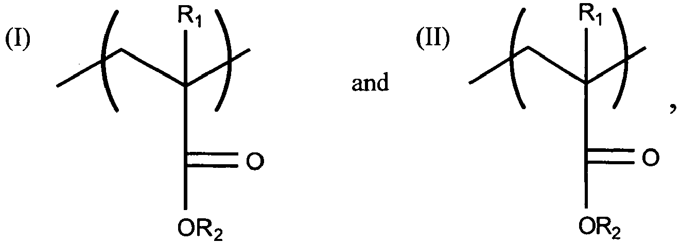 each R1 is individually selected from the group consisting of -H, and C1-C4 alkyl groups; andeach R2 is individually selected from the group consisting of -H, and silicon-containing moieties selected from the group consisting of
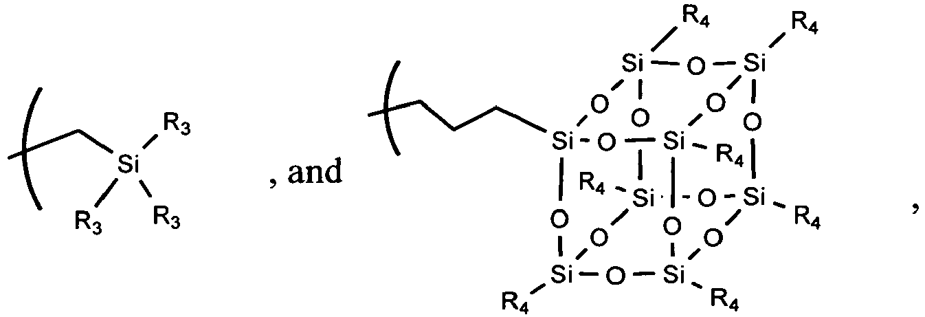 (c) baking said hardmask composition so as to thermally crosslink said hardmask composition and yield a hardmask layer (16);(d) applying a photosensitive composition to form a first imaging layer (18) on top of said hardmask layer (16);(e) exposing said first imaging layer (18) to activating radiation to yield exposed portions in said first imaging layer (18);(f) contacting said first imaging layer (18) with an alkaline developer so as to remove said exposed portions of said first imaging layer (18), wherein said contacting also results in the removal of portions of said hardmask layer (16) beneath said exposed portions in said first imaging layer (18), yielding a patterned hardmask layer (16);(g) contacting said first imaging layer (18) with an organic solvent so as to remove said first imaging layer (18); and(h) applying a second photosensitive composition to form a second imaging layer (18') on top of said patterned hardmask layer (16), without applying additional hardmask composition to said substrate (10).
 - The method of claim 1, further comprising the step of applying an intermediate layer (14) to said substrate prior to applying said hardmask layer (16).
- The method of claim 1, wherein no dry etching occurs during (a)-(h).
- The method of claim 1, wherein said first imaging layer (18) is a photoresist.
- The method of claim 1, wherein said first imaging layer (18) has a thickness of from 20 nm to 200 nm.
- The method of claim 1, said hardmask layer (16) having an initial solubility in a base developer, wherein:
said exposing (e) further comprises exposing at least a portion of said hardmask layer (16) to activating radiation to yield exposed portions of said hardmask layer (16), said exposed portions of said hardmask layer (16) having a final solubility in base developer, said final solubility being greater than said initial solubility. - The method of claim 1, further comprising:(i) exposing said second imaging layer (18') to activating radiation to yield exposed portions in said second imaging layer (18');(j) contacting said second imaging layer (18') with a developer so as to remove said exposed portions, wherein said contacting also results in the removal of portions of said hardmask layer (16) beneath said exposed portions in said second imaging layer (18'), yielding a further patterned hardmask layer (16); and(k) contacting said second imaging layer (18') with an organic solvent so as to remove said second imaging layer (18').
- The method of claim 7, wherein no dry etching occurs during (a)-(k).
- The method of claim 7, further comprising:
(l) transferring the pattern of the patterned hardmask layer (16) formed in (j) to the substrate (10),
preferably further comprising etching said patterned hardmask layer (16) and substrate (10),
wherein the pattern of said patterned hardmask layer (16) preferably comprises vias and trenches (11).
Applications Claiming Priority (2)
| Application Number | Priority Date | Filing Date | Title |
|---|---|---|---|
| US2447408P | 2008-01-29 | 2008-01-29 | |
| PCT/US2009/032446 WO2009097436A2 (en) | 2008-01-29 | 2009-01-29 | On-track process for patterning hardmask by multiple dark field exposures |
Publications (3)
| Publication Number | Publication Date |
|---|---|
| EP2245512A2 EP2245512A2 (en) | 2010-11-03 |
| EP2245512A4 EP2245512A4 (en) | 2011-08-10 |
| EP2245512B1 true EP2245512B1 (en) | 2019-09-11 |
Family
ID=40899576
Family Applications (1)
| Application Number | Title | Priority Date | Filing Date |
|---|---|---|---|
| EP09706292.1A Active EP2245512B1 (en) | 2008-01-29 | 2009-01-29 | On-track process for patterning hardmask by multiple dark field exposures |
Country Status (7)
| Country | Link |
|---|---|
| US (2) | US8133659B2 (en) |
| EP (1) | EP2245512B1 (en) |
| JP (1) | JP5357186B2 (en) |
| KR (1) | KR101647158B1 (en) |
| CN (1) | CN101971102B (en) |
| TW (1) | TWI467337B (en) |
| WO (1) | WO2009097436A2 (en) |
Families Citing this family (26)
| Publication number | Priority date | Publication date | Assignee | Title |
|---|---|---|---|---|
| JP5357186B2 (en) | 2008-01-29 | 2013-12-04 | ブルーワー サイエンス アイ エヌ シー. | On-track process for hard mask pattern formation by multiple dark field exposure |
| US9640396B2 (en) | 2009-01-07 | 2017-05-02 | Brewer Science Inc. | Spin-on spacer materials for double- and triple-patterning lithography |
| US20110086312A1 (en) * | 2009-10-09 | 2011-04-14 | Dammel Ralph R | Positive-Working Photoimageable Bottom Antireflective Coating |
| KR20130039727A (en) * | 2010-03-18 | 2013-04-22 | 보드 오브 리전츠, 더 유니버시티 오브 텍사스 시스템 | Silicon-containing block co-polymers, methods for synthesis and use |
| US8382997B2 (en) * | 2010-08-16 | 2013-02-26 | Tokyo Electron Limited | Method for high aspect ratio patterning in a spin-on layer |
| WO2012087244A1 (en) * | 2010-12-21 | 2012-06-28 | Agency For Science, Technology And Research | Copolymer, composition and method for modifying rheology |
| US8808969B2 (en) | 2011-04-12 | 2014-08-19 | Brewer Science Inc. | Method of making radiation-sensitive sol-gel materials |
| US8647809B2 (en) * | 2011-07-07 | 2014-02-11 | Brewer Science Inc. | Metal-oxide films from small molecules for lithographic applications |
| KR20130015145A (en) * | 2011-08-02 | 2013-02-13 | 삼성전자주식회사 | Method of forming fine patterns for semiconductor device |
| US8759225B2 (en) * | 2012-09-04 | 2014-06-24 | Taiwan Semiconductor Manufacturing Co., Ltd. | Method to form a CMOS image sensor |
| US8795774B2 (en) | 2012-09-23 | 2014-08-05 | Rohm And Haas Electronic Materials Llc | Hardmask |
| US8759220B1 (en) * | 2013-02-28 | 2014-06-24 | Shin-Etsu Chemical Co., Ltd. | Patterning process |
| JP6088999B2 (en) * | 2013-05-02 | 2017-03-01 | 富士フイルム株式会社 | Etching solution and etching solution kit, etching method using the same, and method for manufacturing semiconductor substrate product |
| KR102486400B1 (en) | 2014-01-13 | 2023-01-09 | 어플라이드 머티어리얼스, 인코포레이티드 | Self-aligned double patterning with spatial atomic layer deposition |
| JP6413333B2 (en) * | 2014-05-13 | 2018-10-31 | Jsr株式会社 | Pattern formation method |
| LT3146527T (en) * | 2014-05-22 | 2022-02-25 | Australian Nuclear Science & Technology Organisation | Gamma-ray imaging |
| KR20160029900A (en) * | 2014-09-05 | 2016-03-16 | 삼성전자주식회사 | Method for manufacturing semiconductor device |
| US10095114B2 (en) | 2014-11-14 | 2018-10-09 | Applied Materials, Inc. | Process chamber for field guided exposure and method for implementing the process chamber |
| US20170345643A1 (en) * | 2014-12-24 | 2017-11-30 | Intel Corporation | Photodefinable alignment layer for chemical assisted patterning |
| JP6524594B2 (en) * | 2016-07-07 | 2019-06-05 | パナソニックIpマネジメント株式会社 | Method of manufacturing element chip |
| US20180164685A1 (en) * | 2016-12-14 | 2018-06-14 | Rohm And Haas Electronic Materials Llc | Method using silicon-containing underlayers |
| WO2020117978A1 (en) * | 2018-12-04 | 2020-06-11 | Sunrise Memory Corporation | Methods for forming multilayer horizontal nor-type thin-film memory strings |
| US11650506B2 (en) | 2019-01-18 | 2023-05-16 | Applied Materials Inc. | Film structure for electric field guided photoresist patterning process |
| KR102053921B1 (en) | 2019-03-13 | 2019-12-09 | 영창케미칼 주식회사 | New fine silicon etching pattern forming method in a semiconductor manufacturing process |
| US11429026B2 (en) | 2020-03-20 | 2022-08-30 | Applied Materials, Inc. | Lithography process window enhancement for photoresist patterning |
| KR20240037974A (en) * | 2021-07-28 | 2024-03-22 | 제이에스알 가부시끼가이샤 | Composition for forming a resist underlayer film, method for manufacturing a semiconductor substrate, and method for forming a resist underlayer film |
Family Cites Families (220)
| Publication number | Priority date | Publication date | Assignee | Title |
|---|---|---|---|---|
| US4175175A (en) | 1963-07-16 | 1979-11-20 | Union Carbide Corporation | Polyarylene polyethers |
| USB392136I5 (en) | 1964-08-26 | |||
| US3561962A (en) | 1966-09-01 | 1971-02-09 | Xerox Corp | Method of image reproduction by photo-polymerization and blushing |
| US3629036A (en) | 1969-02-14 | 1971-12-21 | Shipley Co | The method coating of photoresist on circuit boards |
| US3682641A (en) | 1970-03-23 | 1972-08-08 | Du Pont | Photoresist developer extender baths containing polyoxyalkylene ethers and esters and process of use |
| US3615615A (en) | 1970-04-13 | 1971-10-26 | Eastman Kodak Co | Photographic emulsions including reactive quaternary salts |
| US3833374A (en) | 1970-07-14 | 1974-09-03 | Metalphoto Corp | Coloring of anodized aluminum |
| US3894163A (en) | 1971-03-08 | 1975-07-08 | Western Electric Co | Additives to negative photoresists which increase the sensitivity thereof |
| US3856751A (en) | 1972-06-14 | 1974-12-24 | Eastman Kodak Co | Diacid-xanthylium ion polyester and photographic element comprised thereof |
| US3873361A (en) | 1973-11-29 | 1975-03-25 | Ibm | Method of depositing thin film utilizing a lift-off mask |
| US3976524A (en) | 1974-06-17 | 1976-08-24 | Ibm Corporation | Planarization of integrated circuit surfaces through selective photoresist masking |
| CA1077787A (en) | 1975-11-21 | 1980-05-20 | National Aeronautics And Space Administration | Abrasion resistant coatings for plastic surfaces |
| DE2861696D1 (en) | 1977-09-07 | 1982-04-29 | Ici Plc | Thermoplastic aromatic polyetherketones, a method for their preparation and their application as electrical insulants |
| JPS5471579A (en) | 1977-11-17 | 1979-06-08 | Matsushita Electric Ind Co Ltd | Electron beam resist |
| US4244799A (en) | 1978-09-11 | 1981-01-13 | Bell Telephone Laboratories, Incorporated | Fabrication of integrated circuits utilizing thick high-resolution patterns |
| US4244798A (en) | 1979-10-29 | 1981-01-13 | General Motors Corporation | Exhaust electrode process for exhaust gas oxygen sensor |
| US4369090A (en) | 1980-11-06 | 1983-01-18 | Texas Instruments Incorporated | Process for etching sloped vias in polyimide insulators |
| US4430419A (en) | 1981-01-22 | 1984-02-07 | Nippon Telegraph & Telephone Public Corporation | Positive resist and method for manufacturing a pattern thereof |
| US4397722A (en) | 1981-12-31 | 1983-08-09 | International Business Machines Corporation | Polymers from aromatic silanes and process for their preparation |
| US4910122A (en) | 1982-09-30 | 1990-03-20 | Brewer Science, Inc. | Anti-reflective coating |
| US4526856A (en) | 1983-05-23 | 1985-07-02 | Allied Corporation | Low striation positive diazoketone resist composition with cyclic ketone(s) and aliphatic alcohol as solvents |
| US4996247A (en) | 1984-02-10 | 1991-02-26 | General Electric Company | Enhancing color stability to sterilizing radiation of polymer compositions |
| US4568631A (en) | 1984-04-30 | 1986-02-04 | International Business Machines Corporation | Process for delineating photoresist lines at pattern edges only using image reversal composition with diazoquinone |
| JPS60262150A (en) | 1984-06-11 | 1985-12-25 | Nippon Telegr & Teleph Corp <Ntt> | Intermediate layer for 3-layer resist material and method for using it |
| DE3425063A1 (en) | 1984-07-07 | 1986-02-06 | Licentia Patent-Verwaltungs-Gmbh, 6000 Frankfurt | MASK FOR X-RAY LITHOGRAPHY |
| US4578328A (en) | 1984-07-09 | 1986-03-25 | General Electric Company | Photopatternable polyimide compositions and method for making |
| US4683024A (en) | 1985-02-04 | 1987-07-28 | American Telephone And Telegraph Company, At&T Bell Laboratories | Device fabrication method using spin-on glass resins |
| US4732841A (en) | 1986-03-24 | 1988-03-22 | Fairchild Semiconductor Corporation | Tri-level resist process for fine resolution photolithography |
| US4742152A (en) | 1986-05-27 | 1988-05-03 | United Technologies Corporation | High temperature fluorinated polyimides |
| US5091047A (en) | 1986-09-11 | 1992-02-25 | National Semiconductor Corp. | Plasma etching using a bilayer mask |
| US4808513A (en) | 1987-04-06 | 1989-02-28 | Morton Thiokol, Inc. | Method of developing a high contrast, positive photoresist using a developer containing alkanolamine |
| US4927736A (en) | 1987-07-21 | 1990-05-22 | Hoechst Celanese Corporation | Hydroxy polyimides and high temperature positive photoresists therefrom |
| JP2557898B2 (en) | 1987-07-31 | 1996-11-27 | 株式会社東芝 | Semiconductor device |
| US5137780A (en) | 1987-10-16 | 1992-08-11 | The Curators Of The University Of Missouri | Article having a composite insulative coating |
| US4803147A (en) | 1987-11-24 | 1989-02-07 | Hoechst Celanese Corporation | Photosensitive polyimide polymer compositions |
| US4847517A (en) * | 1988-02-16 | 1989-07-11 | Ltv Aerospace & Defense Co. | Microwave tube modulator |
| US4845265A (en) | 1988-02-29 | 1989-07-04 | Allied-Signal Inc. | Polyfunctional vinyl ether terminated ester oligomers |
| US4891303A (en) | 1988-05-26 | 1990-01-02 | Texas Instruments Incorporated | Trilayer microlithographic process using a silicon-based resist as the middle layer |
| KR910000832A (en) | 1988-06-28 | 1991-01-30 | 랄프 챨스 메더스트 | Low dielectric constant and low moisture absorption polyimide and copolyimide for interlevel dielectric and substrate coatings |
| US5304626A (en) | 1988-06-28 | 1994-04-19 | Amoco Corporation | Polyimide copolymers containing 3,3',4,4'-tetracarboxybiphenyl dianhydride (BPDA) moieties |
| DE3835737A1 (en) | 1988-10-20 | 1990-04-26 | Ciba Geigy Ag | POSITIVE FOTORESISTS WITH INCREASED THERMAL STABILITY |
| US5024922A (en) | 1988-11-07 | 1991-06-18 | Moss Mary G | Positive working polyamic acid/imide and diazoquinone photoresist with high temperature pre-bake |
| US5169494A (en) | 1989-03-27 | 1992-12-08 | Matsushita Electric Industrial Co., Ltd. | Fine pattern forming method |
| US5057399A (en) | 1989-03-31 | 1991-10-15 | Tony Flaim | Method for making polyimide microlithographic compositions soluble in alkaline media |
| US5198153A (en) | 1989-05-26 | 1993-03-30 | International Business Machines Corporation | Electrically conductive polymeric |
| US5246782A (en) | 1990-12-10 | 1993-09-21 | The Dow Chemical Company | Laminates of polymers having perfluorocyclobutane rings and polymers containing perfluorocyclobutane rings |
| KR950011927B1 (en) | 1989-12-07 | 1995-10-12 | 가부시끼가이샤 도시바 | Photosensitive composition and resin encapsulated semiconductor device |
| US5132774A (en) | 1990-02-05 | 1992-07-21 | Mitsubishi Denki Kabushiki Kaisha | Semiconductor device including interlayer insulating film |
| US5126231A (en) | 1990-02-26 | 1992-06-30 | Applied Materials, Inc. | Process for multi-layer photoresist etching with minimal feature undercut and unchanging photoresist load during etch |
| US5066566A (en) | 1990-07-31 | 1991-11-19 | At&T Bell Laboratories | Resist materials |
| JP3041972B2 (en) | 1991-01-10 | 2000-05-15 | 富士通株式会社 | Method for manufacturing semiconductor device |
| JPH0613290A (en) * | 1991-10-21 | 1994-01-21 | Dainippon Printing Co Ltd | Pattern transfer method using phase shift photomask |
| DE69331471T2 (en) | 1992-07-22 | 2002-06-20 | Asahi Kasei K.K., Osaka | Photosensitive polyimide precursor composition |
| US5370969A (en) | 1992-07-28 | 1994-12-06 | Sharp Kabushiki Kaisha | Trilayer lithographic process |
| JPH06230574A (en) | 1993-02-05 | 1994-08-19 | Fuji Photo Film Co Ltd | Positive type photosensitive composition |
| US5443941A (en) | 1993-03-01 | 1995-08-22 | National Semiconductor Corporation | Plasma polymer antireflective coating |
| US5397684A (en) | 1993-04-27 | 1995-03-14 | International Business Machines Corporation | Antireflective polyimide dielectric for photolithography |
| JPH07183194A (en) | 1993-12-24 | 1995-07-21 | Sony Corp | Multilayer resist pattern forming method |
| US5691101A (en) | 1994-03-15 | 1997-11-25 | Kabushiki Kaisha Toshiba | Photosensitive composition |
| GB2288184A (en) | 1994-03-31 | 1995-10-11 | Catalysts & Chem Ind Co | Coating composition |
| JPH07283112A (en) * | 1994-04-08 | 1995-10-27 | Hitachi Ltd | Method and apparatus for forming resist pattern |
| US5667940A (en) | 1994-05-11 | 1997-09-16 | United Microelectronics Corporation | Process for creating high density integrated circuits utilizing double coating photoresist mask |
| JP3033443B2 (en) | 1994-06-29 | 2000-04-17 | 信越化学工業株式会社 | Anti-reflective coating material |
| US5607824A (en) | 1994-07-27 | 1997-03-04 | International Business Machines Corporation | Antireflective coating for microlithography |
| JPH08110638A (en) | 1994-10-13 | 1996-04-30 | Hitachi Chem Co Ltd | Photosensitive resin composition and method for producing resist image |
| US5688987A (en) | 1994-11-09 | 1997-11-18 | Brewer Science, Inc. | Non-subliming Mid-UV dyes and ultra-thin organic arcs having differential solubility |
| US5554473A (en) | 1994-11-23 | 1996-09-10 | Mitsubishi Chemical America, Inc. | Photoreceptor having charge transport layers containing a copolycarbonate and layer containing same |
| US5542971A (en) | 1994-12-01 | 1996-08-06 | Pitney Bowes | Bar codes using luminescent invisible inks |
| JPH08250400A (en) * | 1995-03-14 | 1996-09-27 | Mitsubishi Electric Corp | Silicone resin removal method |
| US5545588A (en) | 1995-05-05 | 1996-08-13 | Taiwan Semiconductor Manufacturing Company | Method of using disposable hard mask for gate critical dimension control |
| DE69628613T2 (en) | 1995-07-12 | 2004-04-29 | Mitsubishi Engineering-Plastics Corp. | Polycarbonate resin composition |
| US5968324A (en) | 1995-12-05 | 1999-10-19 | Applied Materials, Inc. | Method and apparatus for depositing antireflective coating |
| KR100223329B1 (en) | 1995-12-29 | 1999-10-15 | 김영환 | Method for manufacturing fine pattern of semiconductor device |
| KR100206597B1 (en) | 1995-12-29 | 1999-07-01 | 김영환 | Manufacturing method of fine pattern of semiconductor device |
| DE69708787T2 (en) | 1996-03-06 | 2002-06-20 | Clariant Finance (Bvi) Ltd., Road Town | METHOD FOR PRODUCING FILM PATTERNS USING LIFTING TECHNOLOGY |
| US5633210A (en) | 1996-04-29 | 1997-05-27 | Taiwan Semiconductor Manufacturing Company, Ltd. | Method for forming damage free patterned layers adjoining the edges of high step height apertures |
| US5807790A (en) | 1996-05-07 | 1998-09-15 | Advanced Micro Devices, Inc. | Selective i-line BARL etch process |
| US5861231A (en) | 1996-06-11 | 1999-01-19 | Shipley Company, L.L.C. | Copolymers and photoresist compositions comprising copolymer resin binder component |
| US5739254A (en) | 1996-08-29 | 1998-04-14 | Xerox Corporation | Process for haloalkylation of high performance polymers |
| KR100194813B1 (en) | 1996-12-05 | 1999-06-15 | 정선종 | Packet Switching Device with Multichannel / Multicast Switching Function and Packet Switching System Using the Same |
| US5952448A (en) | 1996-12-31 | 1999-09-14 | Korea Research Institute Of Chemical Technology | Stable precursor of polyimide and a process for preparing the same |
| TW432257B (en) | 1997-01-31 | 2001-05-01 | Shinetsu Chemical Co | High molecular weight silicone compound, chemically amplified positive resist composition and patterning method |
| US6232386B1 (en) | 1997-02-26 | 2001-05-15 | Integument Technologies, Inc. | Polymer composites having an oxyhalo surface and methods for making same |
| JP3766165B2 (en) | 1997-03-07 | 2006-04-12 | 株式会社ニコン | Image forming method and photosensitive material |
| WO1998039496A1 (en) | 1997-03-07 | 1998-09-11 | Corning Incorporated | Method of making titania-doped fused silica |
| TW473653B (en) | 1997-05-27 | 2002-01-21 | Clariant Japan Kk | Composition for anti-reflective film or photo absorption film and compound used therein |
| US6428894B1 (en) | 1997-06-04 | 2002-08-06 | International Business Machines Corporation | Tunable and removable plasma deposited antireflective coatings |
| US6054254A (en) | 1997-07-03 | 2000-04-25 | Kabushiki Kaisha Toshiba | Composition for underlying film and method of forming a pattern using the film |
| JP3473887B2 (en) | 1997-07-16 | 2003-12-08 | 東京応化工業株式会社 | Composition for forming antireflection film and method for forming resist pattern using the same |
| US6124077A (en) | 1997-09-05 | 2000-09-26 | Kansai Paint Co., Ltd. | Visible light-sensitive compositions and pattern formation process |
| KR100566042B1 (en) | 1997-10-07 | 2006-05-25 | 간사이 페인트 가부시키가이샤 | Positive Electrodeposition Photoresist Composition and Process for Preparing Pattern |
| US6218292B1 (en) | 1997-12-18 | 2001-04-17 | Advanced Micro Devices, Inc. | Dual layer bottom anti-reflective coating |
| US6338936B1 (en) | 1998-02-02 | 2002-01-15 | Taiyo Ink Manufacturing Co., Ltd. | Photosensitive resin composition and method for formation of resist pattern by use thereof |
| US5998569A (en) | 1998-03-17 | 1999-12-07 | International Business Machines Corporation | Environmentally stable optical filter materials |
| US6156665A (en) | 1998-04-13 | 2000-12-05 | Lucent Technologies Inc. | Trilayer lift-off process for semiconductor device metallization |
| US6451498B1 (en) | 1998-05-28 | 2002-09-17 | Atotech Deutschland Gmbh | Photosensitive composition |
| JP3673399B2 (en) | 1998-06-03 | 2005-07-20 | クラリアント インターナショナル リミテッド | Anti-reflection coating composition |
| US6063547A (en) | 1998-06-11 | 2000-05-16 | Chartered Semiconductor Manufacturing, Ltd. | Physical vapor deposition poly-p-phenylene sulfide film as a bottom anti-reflective coating on polysilicon |
| US6121098A (en) | 1998-06-30 | 2000-09-19 | Infineon Technologies North America Corporation | Semiconductor manufacturing method |
| US6976904B2 (en) | 1998-07-09 | 2005-12-20 | Li Family Holdings, Ltd. | Chemical mechanical polishing slurry |
| US6103456A (en) | 1998-07-22 | 2000-08-15 | Siemens Aktiengesellschaft | Prevention of photoresist poisoning from dielectric antireflective coating in semiconductor fabrication |
| US6071662A (en) | 1998-07-23 | 2000-06-06 | Xerox Corporation | Imaging member with improved anti-curl backing layer |
| TWI250379B (en) | 1998-08-07 | 2006-03-01 | Az Electronic Materials Japan | Chemical amplified radiation-sensitive composition which contains onium salt and generator |
| US6268282B1 (en) | 1998-09-03 | 2001-07-31 | Micron Technology, Inc. | Semiconductor processing methods of forming and utilizing antireflective material layers, and methods of forming transistor gate stacks |
| US6380611B1 (en) | 1998-09-03 | 2002-04-30 | Micron Technology, Inc. | Treatment for film surface to reduce photo footing |
| US20020102483A1 (en) | 1998-09-15 | 2002-08-01 | Timothy Adams | Antireflective coating compositions |
| US6361833B1 (en) | 1998-10-28 | 2002-03-26 | Henkel Corporation | Composition and process for treating metal surfaces |
| US6127070A (en) | 1998-12-01 | 2000-10-03 | Advanced Micro Devices, Inc. | Thin resist with nitride hard mask for via etch application |
| US6162587A (en) | 1998-12-01 | 2000-12-19 | Advanced Micro Devices | Thin resist with transition metal hard mask for via etch application |
| US6165695A (en) | 1998-12-01 | 2000-12-26 | Advanced Micro Devices, Inc. | Thin resist with amorphous silicon hard mask for via etch application |
| US6200907B1 (en) | 1998-12-02 | 2001-03-13 | Advanced Micro Devices, Inc. | Ultra-thin resist and barrier metal/oxide hard mask for metal etch |
| US6020269A (en) | 1998-12-02 | 2000-02-01 | Advanced Micro Devices, Inc. | Ultra-thin resist and nitride/oxide hard mask for metal etch |
| US6306560B1 (en) | 1998-12-02 | 2001-10-23 | Advanced Micro Devices, Inc. | Ultra-thin resist and SiON/oxide hard mask for metal etch |
| US6171763B1 (en) | 1998-12-02 | 2001-01-09 | Advanced Micro Devices, Inc. | Ultra-thin resist and oxide/nitride hard mask for metal etch |
| US6156658A (en) | 1998-12-02 | 2000-12-05 | Advanced Micro Devices, Inc. | Ultra-thin resist and silicon/oxide hard mask for metal etch |
| US6309926B1 (en) | 1998-12-04 | 2001-10-30 | Advanced Micro Devices | Thin resist with nitride hard mask for gate etch application |
| US6046112A (en) | 1998-12-14 | 2000-04-04 | Taiwan Semiconductor Manufacturing Company | Chemical mechanical polishing slurry |
| US6207238B1 (en) | 1998-12-16 | 2001-03-27 | Battelle Memorial Institute | Plasma enhanced chemical deposition for high and/or low index of refraction polymers |
| US6251562B1 (en) | 1998-12-23 | 2001-06-26 | International Business Machines Corporation | Antireflective polymer and method of use |
| KR100363695B1 (en) | 1998-12-31 | 2003-04-11 | 주식회사 하이닉스반도체 | Organic diffuse reflection prevention polymer and its manufacturing method |
| US6136511A (en) | 1999-01-20 | 2000-10-24 | Micron Technology, Inc. | Method of patterning substrates using multilayer resist processing |
| US6136679A (en) | 1999-03-05 | 2000-10-24 | Taiwan Semiconductor Manufacturing Company | Gate micro-patterning process |
| US6316165B1 (en) | 1999-03-08 | 2001-11-13 | Shipley Company, L.L.C. | Planarizing antireflective coating compositions |
| US6426125B1 (en) | 1999-03-17 | 2002-07-30 | General Electric Company | Multilayer article and method of making by ARC plasma deposition |
| US6616692B1 (en) | 1999-04-30 | 2003-09-09 | Advanced Medical Optics, Inc. | Intraocular lens combinations |
| US6458509B1 (en) | 1999-04-30 | 2002-10-01 | Toagosei Co., Ltd. | Resist compositions |
| US6890448B2 (en) * | 1999-06-11 | 2005-05-10 | Shipley Company, L.L.C. | Antireflective hard mask compositions |
| US6110653A (en) | 1999-07-26 | 2000-08-29 | International Business Machines Corporation | Acid sensitive ARC and method of use |
| JP4512217B2 (en) | 1999-08-20 | 2010-07-28 | 富士フイルム株式会社 | Arylsilane compound, light emitting device material, and light emitting device using the same |
| CN1658375B (en) | 1999-08-26 | 2011-03-30 | 布鲁尔科技公司 | Fill material for dual damascene processes |
| US6852473B2 (en) | 2000-01-12 | 2005-02-08 | Infineon Technologies Richmond, Lp | Anti-reflective coating conformality control |
| US20020009599A1 (en) | 2000-01-26 | 2002-01-24 | Welch Cletus N. | Photochromic polyurethane coating and articles having such a coating |
| TW439118B (en) | 2000-02-10 | 2001-06-07 | Winbond Electronics Corp | Multilayer thin photoresist process |
| EP1269258B1 (en) | 2000-02-22 | 2012-01-11 | Brewer Science, Inc. | Organic polymeric antireflective coatings deposited by chemical vapor deposition |
| US6461717B1 (en) | 2000-04-24 | 2002-10-08 | Shipley Company, L.L.C. | Aperture fill |
| JP2001344732A (en) | 2000-05-29 | 2001-12-14 | Fujitsu Ltd | Magnetic recording medium substrate, method of manufacturing the same, and method of evaluating magnetic recording medium |
| JP2001338926A (en) | 2000-05-29 | 2001-12-07 | Sony Corp | Method for manufacturing semiconductor device |
| TW556047B (en) | 2000-07-31 | 2003-10-01 | Shipley Co Llc | Coated substrate, method for forming photoresist relief image, and antireflective composition |
| KR100917101B1 (en) | 2000-08-04 | 2009-09-15 | 도요 보세키 가부시키가이샤 | Flexible metal laminate and production method thereof |
| WO2002025374A2 (en) | 2000-09-19 | 2002-03-28 | Shipley Company, L.L.C. | Antireflective composition |
| US6455416B1 (en) | 2000-10-24 | 2002-09-24 | Advanced Micro Devices, Inc. | Developer soluble dyed BARC for dual damascene process |
| KR100669862B1 (en) * | 2000-11-13 | 2007-01-17 | 삼성전자주식회사 | Method of forming fine pattern of semiconductor device |
| US20030054117A1 (en) | 2001-02-02 | 2003-03-20 | Brewer Science, Inc. | Polymeric antireflective coatings deposited by plasma enhanced chemical vapor deposition |
| US6444582B1 (en) | 2001-02-05 | 2002-09-03 | United Microelectronics Corp. | Methods for removing silicon-oxy-nitride layer and wafer surface cleaning |
| US6309955B1 (en) | 2001-02-16 | 2001-10-30 | Advanced Micro Devices, Inc. | Method for using a CVD organic barc as a hard mask during via etch |
| US6852828B2 (en) | 2001-02-16 | 2005-02-08 | Medtronic, Inc. | Poly amic acid system for polyimides |
| US6383952B1 (en) | 2001-02-28 | 2002-05-07 | Advanced Micro Devices, Inc. | RELACS process to double the frequency or pitch of small feature formation |
| TW576859B (en) | 2001-05-11 | 2004-02-21 | Shipley Co Llc | Antireflective coating compositions |
| US6680252B2 (en) | 2001-05-15 | 2004-01-20 | United Microelectronics Corp. | Method for planarizing barc layer in dual damascene process |
| AU2002312945A1 (en) | 2001-05-29 | 2002-12-09 | Essilor International Compagnie Generale D'optique | Method for forming on-site a coated optical article |
| US6605545B2 (en) | 2001-06-01 | 2003-08-12 | United Microelectronics Corp. | Method for forming hybrid low-K film stack to avoid thermal stress effect |
| US6458705B1 (en) | 2001-06-06 | 2002-10-01 | United Microelectronics Corp. | Method for forming via-first dual damascene interconnect structure |
| US6548387B2 (en) | 2001-07-20 | 2003-04-15 | United Microelectronics Corporation | Method for reducing hole defects in the polysilicon layer |
| US6624068B2 (en) | 2001-08-24 | 2003-09-23 | Texas Instruments Incorporated | Polysilicon processing using an anti-reflective dual layer hardmask for 193 nm lithography |
| US6586560B1 (en) | 2001-09-18 | 2003-07-01 | Microchem Corp. | Alkaline soluble maleimide-containing polymers |
| EP1448669B1 (en) | 2001-09-27 | 2010-04-07 | LG Chem Ltd. | Adhesive composition comprising a polyimide copolymer and method for preparing the same |
| KR100465866B1 (en) | 2001-10-26 | 2005-01-13 | 주식회사 하이닉스반도체 | Organic anti-reflective coating material and preparation thereof |
| US6916537B2 (en) | 2001-11-01 | 2005-07-12 | Transitions Optical Inc. | Articles having a photochromic polymeric coating |
| JP2003162065A (en) | 2001-11-26 | 2003-06-06 | Mitsubishi Electric Corp | Exposure device, exposure mask, exposure method, display device, and electronic component |
| JP3773445B2 (en) | 2001-12-19 | 2006-05-10 | セントラル硝子株式会社 | Fluorine-containing alicyclic diamine and polymer using the same |
| US20030215736A1 (en) | 2002-01-09 | 2003-11-20 | Oberlander Joseph E. | Negative-working photoimageable bottom antireflective coating |
| US6844131B2 (en) | 2002-01-09 | 2005-01-18 | Clariant Finance (Bvi) Limited | Positive-working photoimageable bottom antireflective coating |
| US7070914B2 (en) | 2002-01-09 | 2006-07-04 | Az Electronic Materials Usa Corp. | Process for producing an image using a first minimum bottom antireflective coating composition |
| US7261997B2 (en) | 2002-01-17 | 2007-08-28 | Brewer Science Inc. | Spin bowl compatible polyamic acids/imides as wet developable polymer binders for anti-reflective coatings |
| US6488509B1 (en) | 2002-01-23 | 2002-12-03 | Taiwan Semiconductor Manufacturing Company | Plug filling for dual-damascene process |
| KR20030068729A (en) | 2002-02-16 | 2003-08-25 | 삼성전자주식회사 | Compositions for forming anti-reflective light absorbing layer and method for formimg patterns of semiconductor device using the same |
| US6911293B2 (en) | 2002-04-11 | 2005-06-28 | Clariant Finance (Bvi) Limited | Photoresist compositions comprising acetals and ketals as solvents |
| US6852474B2 (en) | 2002-04-30 | 2005-02-08 | Brewer Science Inc. | Polymeric antireflective coatings deposited by plasma enhanced chemical vapor deposition |
| US6849293B2 (en) | 2002-05-02 | 2005-02-01 | Institute Of Microelectronics | Method to minimize iso-dense contact or via gap filling variation of polymeric materials in the spin coat process |
| US7265431B2 (en) | 2002-05-17 | 2007-09-04 | Intel Corporation | Imageable bottom anti-reflective coating for high resolution lithography |
| US6872506B2 (en) | 2002-06-25 | 2005-03-29 | Brewer Science Inc. | Wet-developable anti-reflective compositions |
| US6740469B2 (en) * | 2002-06-25 | 2004-05-25 | Brewer Science Inc. | Developer-soluble metal alkoxide coatings for microelectronic applications |
| US6638853B1 (en) | 2002-07-03 | 2003-10-28 | Taiwan Semiconductor Manufacturing Co. Ltd. | Method for avoiding photoresist resist residue on semioconductor feature sidewalls |
| KR20040009384A (en) | 2002-07-23 | 2004-01-31 | 삼성전자주식회사 | Photoresist developer soluble organic bottom anti-reflective composition and photolithography and etching process using the same |
| US7108958B2 (en) | 2002-07-31 | 2006-09-19 | Brewer Science Inc. | Photosensitive bottom anti-reflective coatings |
| US6566280B1 (en) | 2002-08-26 | 2003-05-20 | Intel Corporation | Forming polymer features on a substrate |
| US6821689B2 (en) | 2002-09-16 | 2004-11-23 | Numerical Technologies | Using second exposure to assist a PSM exposure in printing a tight space adjacent to large feature |
| US20040077173A1 (en) | 2002-10-17 | 2004-04-22 | Swaminathan Sivakumar | Using water soluble bottom anti-reflective coating |
| JP4433160B2 (en) * | 2003-01-30 | 2010-03-17 | 信越化学工業株式会社 | Polymer compound, resist material, and pattern forming method |
| US7135269B2 (en) * | 2003-01-30 | 2006-11-14 | Shin-Etsu Chemical Co., Ltd. | Polymer, resist composition and patterning process |
| US7507783B2 (en) * | 2003-02-24 | 2009-03-24 | Brewer Science Inc. | Thermally curable middle layer comprising polyhedral oligomeric silsesouioxanes for 193-nm trilayer resist process |
| KR100487948B1 (en) | 2003-03-06 | 2005-05-06 | 삼성전자주식회사 | Method of forming a via contact structure using a dual damascene technique |
| KR100539494B1 (en) | 2003-05-02 | 2005-12-29 | 한국전자통신연구원 | Polyamic ester having moieties of electro and nonlinear optic compound in side chains as an electro and nonlinear optic polymer, manufacturing method therefor and film manufactured therefrom |
| US7235348B2 (en) | 2003-05-22 | 2007-06-26 | Taiwan Semiconductor Manufacturing Co., Ltd. | Water soluble negative tone photoresist |
| WO2004113417A1 (en) | 2003-05-23 | 2004-12-29 | Dow Corning Corporation | Siloxane resin-based anti-reflective coating composition having high wet etch rate |
| US7364832B2 (en) | 2003-06-11 | 2008-04-29 | Brewer Science Inc. | Wet developable hard mask in conjunction with thin photoresist for micro photolithography |
| US7172849B2 (en) * | 2003-08-22 | 2007-02-06 | International Business Machines Corporation | Antireflective hardmask and uses thereof |
| US7074527B2 (en) | 2003-09-23 | 2006-07-11 | Freescale Semiconductor, Inc. | Method for fabricating a mask using a hardmask and method for making a semiconductor device using the same |
| US7270931B2 (en) * | 2003-10-06 | 2007-09-18 | International Business Machines Corporation | Silicon-containing compositions for spin-on ARC/hardmask materials |
| EP1673801B1 (en) | 2003-10-15 | 2014-04-09 | Brewer Science, Inc. | Developer-soluble materials and methods of using the same in via-first dual damascene applications |
| US7064078B2 (en) * | 2004-01-30 | 2006-06-20 | Applied Materials | Techniques for the use of amorphous carbon (APF) for various etch and litho integration scheme |
| US20050214674A1 (en) | 2004-03-25 | 2005-09-29 | Yu Sui | Positive-working photoimageable bottom antireflective coating |
| US20050255410A1 (en) | 2004-04-29 | 2005-11-17 | Guerrero Douglas J | Anti-reflective coatings using vinyl ether crosslinkers |
| US20070207406A1 (en) | 2004-04-29 | 2007-09-06 | Guerrero Douglas J | Anti-reflective coatings using vinyl ether crosslinkers |
| US7012028B2 (en) | 2004-07-26 | 2006-03-14 | Texas Instruments Incorporated | Transistor fabrication methods using reduced width sidewall spacers |
| JP4433933B2 (en) * | 2004-08-13 | 2010-03-17 | Jsr株式会社 | Radiation-sensitive composition and hard mask forming material |
| KR100639680B1 (en) | 2005-01-17 | 2006-10-31 | 삼성전자주식회사 | Method of forming fine pattern of semiconductor device |
| US7390746B2 (en) | 2005-03-15 | 2008-06-24 | Micron Technology, Inc. | Multiple deposition for integration of spacers in pitch multiplication process |
| KR100720243B1 (en) * | 2005-06-22 | 2007-05-22 | 주식회사 하이닉스반도체 | Micro pattern formation method using double exposure process |
| US20070018286A1 (en) * | 2005-07-14 | 2007-01-25 | Asml Netherlands B.V. | Substrate, lithographic multiple exposure method, machine readable medium |
| CN1896869A (en) * | 2005-07-14 | 2007-01-17 | Asml荷兰有限公司 | Substrate, lithographic multiple exposure method, machine readable medium |
| US7776744B2 (en) | 2005-09-01 | 2010-08-17 | Micron Technology, Inc. | Pitch multiplication spacers and methods of forming the same |
| TWI403843B (en) * | 2005-09-13 | 2013-08-01 | Fujifilm Corp | Positive resist composition and pattern-forming method using the same |
| US7824842B2 (en) | 2005-10-05 | 2010-11-02 | Asml Netherlands B.V. | Method of patterning a positive tone resist layer overlaying a lithographic substrate |
| KR100740611B1 (en) * | 2005-10-12 | 2007-07-18 | 삼성전자주식회사 | Polymer for top coating membrane, top coating solution composition and immersion lithography process using the same |
| KR20070087356A (en) | 2006-02-23 | 2007-08-28 | 주식회사 하이닉스반도체 | Method of forming fine pattern of semiconductor device |
| US20070212649A1 (en) | 2006-03-07 | 2007-09-13 | Asml Netherlands B.V. | Method and system for enhanced lithographic patterning |
| US7767385B2 (en) | 2006-03-09 | 2010-08-03 | International Business Machines Corporation | Method for lithography for optimizing process conditions |
| EP1845416A3 (en) | 2006-04-11 | 2009-05-20 | Rohm and Haas Electronic Materials, L.L.C. | Coating compositions for photolithography |
| US7429533B2 (en) | 2006-05-10 | 2008-09-30 | Lam Research Corporation | Pitch reduction |
| JP2007311508A (en) * | 2006-05-17 | 2007-11-29 | Nikon Corp | Fine pattern forming method and device manufacturing method |
| US7435537B2 (en) * | 2006-06-21 | 2008-10-14 | International Business Machines Corporation | Fluorinated half ester of maleic anhydride polymers for dry 193 nm top antireflective coating application |
| US7914974B2 (en) | 2006-08-18 | 2011-03-29 | Brewer Science Inc. | Anti-reflective imaging layer for multiple patterning process |
| JP4826805B2 (en) * | 2006-08-30 | 2011-11-30 | 信越化学工業株式会社 | Photoresist underlayer film material, photoresist underlayer film substrate, and pattern forming method |
| US7862985B2 (en) * | 2006-09-22 | 2011-01-04 | Tokyo Electron Limited | Method for double patterning a developable anti-reflective coating |
| US8168372B2 (en) * | 2006-09-25 | 2012-05-01 | Brewer Science Inc. | Method of creating photolithographic structures with developer-trimmed hard mask |
| TWI374478B (en) | 2007-02-13 | 2012-10-11 | Rohm & Haas Elect Mat | Electronic device manufacture |
| JP5671202B2 (en) | 2007-10-26 | 2015-02-18 | アプライド マテリアルズ インコーポレイテッドApplied Materials,Incorporated | How to double the frequency using a photoresist template mask |
| JP5357186B2 (en) | 2008-01-29 | 2013-12-04 | ブルーワー サイエンス アイ エヌ シー. | On-track process for hard mask pattern formation by multiple dark field exposure |
| US9640396B2 (en) | 2009-01-07 | 2017-05-02 | Brewer Science Inc. | Spin-on spacer materials for double- and triple-patterning lithography |
-
2009
- 2009-01-29 JP JP2010545164A patent/JP5357186B2/en active Active
- 2009-01-29 US US12/362,268 patent/US8133659B2/en active Active
- 2009-01-29 WO PCT/US2009/032446 patent/WO2009097436A2/en not_active Ceased
- 2009-01-29 EP EP09706292.1A patent/EP2245512B1/en active Active
- 2009-01-29 KR KR1020107017736A patent/KR101647158B1/en active Active
- 2009-01-29 CN CN2009801088816A patent/CN101971102B/en active Active
- 2009-02-02 TW TW098103192A patent/TWI467337B/en active
-
2011
- 2011-05-24 US US13/114,612 patent/US8415083B2/en active Active
Non-Patent Citations (1)
| Title |
|---|
| None * |
Also Published As
| Publication number | Publication date |
|---|---|
| US20090191474A1 (en) | 2009-07-30 |
| US8133659B2 (en) | 2012-03-13 |
| JP5357186B2 (en) | 2013-12-04 |
| TW200947133A (en) | 2009-11-16 |
| JP2011514662A (en) | 2011-05-06 |
| EP2245512A2 (en) | 2010-11-03 |
| CN101971102B (en) | 2012-12-12 |
| CN101971102A (en) | 2011-02-09 |
| US20110223524A1 (en) | 2011-09-15 |
| TWI467337B (en) | 2015-01-01 |
| EP2245512A4 (en) | 2011-08-10 |
| WO2009097436A2 (en) | 2009-08-06 |
| KR20100110363A (en) | 2010-10-12 |
| WO2009097436A3 (en) | 2009-10-15 |
| KR101647158B1 (en) | 2016-08-09 |
| US8415083B2 (en) | 2013-04-09 |
Similar Documents
| Publication | Publication Date | Title |
|---|---|---|
| US8133659B2 (en) | On-track process for patterning hardmask by multiple dark field exposures | |
| EP2399169B1 (en) | Acid-sensitive, developer-soluble bottom anti-reflective coatings | |
| US7939244B2 (en) | Photosensitive hardmask for microlithography | |
| JP6109164B2 (en) | Small molecule derived metal oxide films for lithography applications | |
| EP2841513B1 (en) | Photosensitive, developer-soluble bottom anti-reflective coating material | |
| EP2255377B1 (en) | Method of forming a microelectronic structure comprising dual-layer light-sensitive developer-soluble bottom anti-reflective coatings for 193-nm lithography and layer stack for its formation | |
| EP2089770B1 (en) | Method of creating photolithographic structures with developer-trimmed hard mask | |
| US7364832B2 (en) | Wet developable hard mask in conjunction with thin photoresist for micro photolithography | |
| US7507783B2 (en) | Thermally curable middle layer comprising polyhedral oligomeric silsesouioxanes for 193-nm trilayer resist process | |
| WO2008150058A1 (en) | Hardmask composition having antireflective properties and method of patterning material on substrate using the same | |
| JP2013515972A (en) | Anti-reflective coating composition containing fused aromatic rings | |
| JP4221610B2 (en) | Lithographic gap fill material forming composition containing acrylic polymer | |
| WO2006126406A1 (en) | Polysilane compound-containing lower layer film forming composition for lithography | |
| WO2008075860A1 (en) | High etch resistant hardmask composition having antireflective properties, method for forming patterned material layer using the hardmask composition and semiconductor integrated circuit device produced using the method | |
| WO2006096221A1 (en) | Low refractive index polymers as underlayers for silicon-containing photoresists |
Legal Events
| Date | Code | Title | Description |
|---|---|---|---|
| PUAI | Public reference made under article 153(3) epc to a published international application that has entered the european phase |
Free format text: ORIGINAL CODE: 0009012 |
|
| 17P | Request for examination filed |
Effective date: 20100826 |
|
| AK | Designated contracting states |
Kind code of ref document: A2 Designated state(s): AT BE BG CH CY CZ DE DK EE ES FI FR GB GR HR HU IE IS IT LI LT LU LV MC MK MT NL NO PL PT RO SE SI SK TR |
|
| AX | Request for extension of the european patent |
Extension state: AL BA RS |
|
| DAX | Request for extension of the european patent (deleted) | ||
| A4 | Supplementary search report drawn up and despatched |
Effective date: 20110707 |
|
| RIC1 | Information provided on ipc code assigned before grant |
Ipc: H01L 21/027 20060101ALI20110701BHEP Ipc: G03F 7/26 20060101AFI20110701BHEP |
|
| 17Q | First examination report despatched |
Effective date: 20160809 |
|
| STAA | Information on the status of an ep patent application or granted ep patent |
Free format text: STATUS: EXAMINATION IS IN PROGRESS |
|
| REG | Reference to a national code |
Ref country code: DE Ref legal event code: R079 Ref document number: 602009059791 Country of ref document: DE Free format text: PREVIOUS MAIN CLASS: G03F0007260000 Ipc: G03F0007075000 |
|
| RIC1 | Information provided on ipc code assigned before grant |
Ipc: G03F 7/32 20060101ALI20190401BHEP Ipc: G03F 7/00 20060101ALI20190401BHEP Ipc: G03F 7/095 20060101ALI20190401BHEP Ipc: G03F 7/075 20060101AFI20190401BHEP |
|
| GRAP | Despatch of communication of intention to grant a patent |
Free format text: ORIGINAL CODE: EPIDOSNIGR1 |
|
| STAA | Information on the status of an ep patent application or granted ep patent |
Free format text: STATUS: GRANT OF PATENT IS INTENDED |
|
| INTG | Intention to grant announced |
Effective date: 20190513 |
|
| GRAS | Grant fee paid |
Free format text: ORIGINAL CODE: EPIDOSNIGR3 |
|
| GRAA | (expected) grant |
Free format text: ORIGINAL CODE: 0009210 |
|
| STAA | Information on the status of an ep patent application or granted ep patent |
Free format text: STATUS: THE PATENT HAS BEEN GRANTED |
|
| AK | Designated contracting states |
Kind code of ref document: B1 Designated state(s): AT BE BG CH CY CZ DE DK EE ES FI FR GB GR HR HU IE IS IT LI LT LU LV MC MK MT NL NO PL PT RO SE SI SK TR |
|
| REG | Reference to a national code |
Ref country code: GB Ref legal event code: FG4D |
|
| REG | Reference to a national code |
Ref country code: CH Ref legal event code: EP |
|
| REG | Reference to a national code |
Ref country code: AT Ref legal event code: REF Ref document number: 1179220 Country of ref document: AT Kind code of ref document: T Effective date: 20190915 |
|
| REG | Reference to a national code |
Ref country code: DE Ref legal event code: R096 Ref document number: 602009059791 Country of ref document: DE |
|
| REG | Reference to a national code |
Ref country code: IE Ref legal event code: FG4D |
|
| REG | Reference to a national code |
Ref country code: NL Ref legal event code: MP Effective date: 20190911 |
|
| REG | Reference to a national code |
Ref country code: LT Ref legal event code: MG4D |
|
| PG25 | Lapsed in a contracting state [announced via postgrant information from national office to epo] |
Ref country code: NO Free format text: LAPSE BECAUSE OF FAILURE TO SUBMIT A TRANSLATION OF THE DESCRIPTION OR TO PAY THE FEE WITHIN THE PRESCRIBED TIME-LIMIT Effective date: 20191211 Ref country code: SE Free format text: LAPSE BECAUSE OF FAILURE TO SUBMIT A TRANSLATION OF THE DESCRIPTION OR TO PAY THE FEE WITHIN THE PRESCRIBED TIME-LIMIT Effective date: 20190911 Ref country code: FI Free format text: LAPSE BECAUSE OF FAILURE TO SUBMIT A TRANSLATION OF THE DESCRIPTION OR TO PAY THE FEE WITHIN THE PRESCRIBED TIME-LIMIT Effective date: 20190911 Ref country code: HR Free format text: LAPSE BECAUSE OF FAILURE TO SUBMIT A TRANSLATION OF THE DESCRIPTION OR TO PAY THE FEE WITHIN THE PRESCRIBED TIME-LIMIT Effective date: 20190911 Ref country code: BG Free format text: LAPSE BECAUSE OF FAILURE TO SUBMIT A TRANSLATION OF THE DESCRIPTION OR TO PAY THE FEE WITHIN THE PRESCRIBED TIME-LIMIT Effective date: 20191211 Ref country code: LT Free format text: LAPSE BECAUSE OF FAILURE TO SUBMIT A TRANSLATION OF THE DESCRIPTION OR TO PAY THE FEE WITHIN THE PRESCRIBED TIME-LIMIT Effective date: 20190911 |
|
| PG25 | Lapsed in a contracting state [announced via postgrant information from national office to epo] |
Ref country code: GR Free format text: LAPSE BECAUSE OF FAILURE TO SUBMIT A TRANSLATION OF THE DESCRIPTION OR TO PAY THE FEE WITHIN THE PRESCRIBED TIME-LIMIT Effective date: 20191212 Ref country code: ES Free format text: LAPSE BECAUSE OF FAILURE TO SUBMIT A TRANSLATION OF THE DESCRIPTION OR TO PAY THE FEE WITHIN THE PRESCRIBED TIME-LIMIT Effective date: 20190911 Ref country code: LV Free format text: LAPSE BECAUSE OF FAILURE TO SUBMIT A TRANSLATION OF THE DESCRIPTION OR TO PAY THE FEE WITHIN THE PRESCRIBED TIME-LIMIT Effective date: 20190911 |
|
| REG | Reference to a national code |
Ref country code: AT Ref legal event code: MK05 Ref document number: 1179220 Country of ref document: AT Kind code of ref document: T Effective date: 20190911 |
|
| PG25 | Lapsed in a contracting state [announced via postgrant information from national office to epo] |
Ref country code: RO Free format text: LAPSE BECAUSE OF FAILURE TO SUBMIT A TRANSLATION OF THE DESCRIPTION OR TO PAY THE FEE WITHIN THE PRESCRIBED TIME-LIMIT Effective date: 20190911 Ref country code: PT Free format text: LAPSE BECAUSE OF FAILURE TO SUBMIT A TRANSLATION OF THE DESCRIPTION OR TO PAY THE FEE WITHIN THE PRESCRIBED TIME-LIMIT Effective date: 20200113 Ref country code: PL Free format text: LAPSE BECAUSE OF FAILURE TO SUBMIT A TRANSLATION OF THE DESCRIPTION OR TO PAY THE FEE WITHIN THE PRESCRIBED TIME-LIMIT Effective date: 20190911 Ref country code: EE Free format text: LAPSE BECAUSE OF FAILURE TO SUBMIT A TRANSLATION OF THE DESCRIPTION OR TO PAY THE FEE WITHIN THE PRESCRIBED TIME-LIMIT Effective date: 20190911 Ref country code: NL Free format text: LAPSE BECAUSE OF FAILURE TO SUBMIT A TRANSLATION OF THE DESCRIPTION OR TO PAY THE FEE WITHIN THE PRESCRIBED TIME-LIMIT Effective date: 20190911 Ref country code: AT Free format text: LAPSE BECAUSE OF FAILURE TO SUBMIT A TRANSLATION OF THE DESCRIPTION OR TO PAY THE FEE WITHIN THE PRESCRIBED TIME-LIMIT Effective date: 20190911 Ref country code: IT Free format text: LAPSE BECAUSE OF FAILURE TO SUBMIT A TRANSLATION OF THE DESCRIPTION OR TO PAY THE FEE WITHIN THE PRESCRIBED TIME-LIMIT Effective date: 20190911 |
|
| PG25 | Lapsed in a contracting state [announced via postgrant information from national office to epo] |
Ref country code: CZ Free format text: LAPSE BECAUSE OF FAILURE TO SUBMIT A TRANSLATION OF THE DESCRIPTION OR TO PAY THE FEE WITHIN THE PRESCRIBED TIME-LIMIT Effective date: 20190911 Ref country code: SK Free format text: LAPSE BECAUSE OF FAILURE TO SUBMIT A TRANSLATION OF THE DESCRIPTION OR TO PAY THE FEE WITHIN THE PRESCRIBED TIME-LIMIT Effective date: 20190911 Ref country code: IS Free format text: LAPSE BECAUSE OF FAILURE TO SUBMIT A TRANSLATION OF THE DESCRIPTION OR TO PAY THE FEE WITHIN THE PRESCRIBED TIME-LIMIT Effective date: 20200224 |
|
| REG | Reference to a national code |
Ref country code: DE Ref legal event code: R097 Ref document number: 602009059791 Country of ref document: DE |
|
| PLBE | No opposition filed within time limit |
Free format text: ORIGINAL CODE: 0009261 |
|
| STAA | Information on the status of an ep patent application or granted ep patent |
Free format text: STATUS: NO OPPOSITION FILED WITHIN TIME LIMIT |
|
| PG2D | Information on lapse in contracting state deleted |
Ref country code: IS |
|
| PG25 | Lapsed in a contracting state [announced via postgrant information from national office to epo] |
Ref country code: DK Free format text: LAPSE BECAUSE OF FAILURE TO SUBMIT A TRANSLATION OF THE DESCRIPTION OR TO PAY THE FEE WITHIN THE PRESCRIBED TIME-LIMIT Effective date: 20190911 Ref country code: IS Free format text: LAPSE BECAUSE OF FAILURE TO SUBMIT A TRANSLATION OF THE DESCRIPTION OR TO PAY THE FEE WITHIN THE PRESCRIBED TIME-LIMIT Effective date: 20200112 |
|
| REG | Reference to a national code |
Ref country code: DE Ref legal event code: R119 Ref document number: 602009059791 Country of ref document: DE |
|
| 26N | No opposition filed |
Effective date: 20200615 |
|
| PG25 | Lapsed in a contracting state [announced via postgrant information from national office to epo] |
Ref country code: MC Free format text: LAPSE BECAUSE OF FAILURE TO SUBMIT A TRANSLATION OF THE DESCRIPTION OR TO PAY THE FEE WITHIN THE PRESCRIBED TIME-LIMIT Effective date: 20190911 Ref country code: SI Free format text: LAPSE BECAUSE OF FAILURE TO SUBMIT A TRANSLATION OF THE DESCRIPTION OR TO PAY THE FEE WITHIN THE PRESCRIBED TIME-LIMIT Effective date: 20190911 |
|
| REG | Reference to a national code |
Ref country code: CH Ref legal event code: PL |
|
| REG | Reference to a national code |
Ref country code: BE Ref legal event code: MM Effective date: 20200131 |
|
| PG25 | Lapsed in a contracting state [announced via postgrant information from national office to epo] |
Ref country code: LU Free format text: LAPSE BECAUSE OF NON-PAYMENT OF DUE FEES Effective date: 20200129 Ref country code: FR Free format text: LAPSE BECAUSE OF NON-PAYMENT OF DUE FEES Effective date: 20200131 Ref country code: DE Free format text: LAPSE BECAUSE OF NON-PAYMENT OF DUE FEES Effective date: 20200801 |
|
| PG25 | Lapsed in a contracting state [announced via postgrant information from national office to epo] |
Ref country code: BE Free format text: LAPSE BECAUSE OF NON-PAYMENT OF DUE FEES Effective date: 20200131 Ref country code: CH Free format text: LAPSE BECAUSE OF NON-PAYMENT OF DUE FEES Effective date: 20200131 Ref country code: LI Free format text: LAPSE BECAUSE OF NON-PAYMENT OF DUE FEES Effective date: 20200131 |
|
| PG25 | Lapsed in a contracting state [announced via postgrant information from national office to epo] |
Ref country code: IE Free format text: LAPSE BECAUSE OF NON-PAYMENT OF DUE FEES Effective date: 20200129 |
|
| PG25 | Lapsed in a contracting state [announced via postgrant information from national office to epo] |
Ref country code: TR Free format text: LAPSE BECAUSE OF FAILURE TO SUBMIT A TRANSLATION OF THE DESCRIPTION OR TO PAY THE FEE WITHIN THE PRESCRIBED TIME-LIMIT Effective date: 20190911 Ref country code: MT Free format text: LAPSE BECAUSE OF FAILURE TO SUBMIT A TRANSLATION OF THE DESCRIPTION OR TO PAY THE FEE WITHIN THE PRESCRIBED TIME-LIMIT Effective date: 20190911 Ref country code: CY Free format text: LAPSE BECAUSE OF FAILURE TO SUBMIT A TRANSLATION OF THE DESCRIPTION OR TO PAY THE FEE WITHIN THE PRESCRIBED TIME-LIMIT Effective date: 20190911 |
|
| PG25 | Lapsed in a contracting state [announced via postgrant information from national office to epo] |
Ref country code: MK Free format text: LAPSE BECAUSE OF FAILURE TO SUBMIT A TRANSLATION OF THE DESCRIPTION OR TO PAY THE FEE WITHIN THE PRESCRIBED TIME-LIMIT Effective date: 20190911 |
|
| PGFP | Annual fee paid to national office [announced via postgrant information from national office to epo] |
Ref country code: GB Payment date: 20260127 Year of fee payment: 18 |