EP2242144A2 - Multi-band internal antenna - Google Patents
Multi-band internal antenna Download PDFInfo
- Publication number
- EP2242144A2 EP2242144A2 EP09700969A EP09700969A EP2242144A2 EP 2242144 A2 EP2242144 A2 EP 2242144A2 EP 09700969 A EP09700969 A EP 09700969A EP 09700969 A EP09700969 A EP 09700969A EP 2242144 A2 EP2242144 A2 EP 2242144A2
- Authority
- EP
- European Patent Office
- Prior art keywords
- matching
- matching element
- internal antenna
- band internal
- multi band
- Prior art date
- Legal status (The legal status is an assumption and is not a legal conclusion. Google has not performed a legal analysis and makes no representation as to the accuracy of the status listed.)
- Granted
Links
- 230000005855 radiation Effects 0.000 claims abstract description 62
- 230000008878 coupling Effects 0.000 claims abstract description 50
- 238000010168 coupling process Methods 0.000 claims abstract description 50
- 238000005859 coupling reaction Methods 0.000 claims abstract description 50
- 238000005452 bending Methods 0.000 claims description 4
- 238000013461 design Methods 0.000 abstract description 4
- ORQBXQOJMQIAOY-UHFFFAOYSA-N nobelium Chemical compound [No] ORQBXQOJMQIAOY-UHFFFAOYSA-N 0.000 description 6
- 230000000694 effects Effects 0.000 description 4
- 238000007792 addition Methods 0.000 description 3
- 230000005404 monopole Effects 0.000 description 3
- 238000013459 approach Methods 0.000 description 2
- 239000003989 dielectric material Substances 0.000 description 2
- 230000005670 electromagnetic radiation Effects 0.000 description 2
- 230000004907 flux Effects 0.000 description 2
- 230000003993 interaction Effects 0.000 description 2
- 238000010295 mobile communication Methods 0.000 description 2
- 230000003071 parasitic effect Effects 0.000 description 2
- 238000010521 absorption reaction Methods 0.000 description 1
- 230000004075 alteration Effects 0.000 description 1
- 230000002238 attenuated effect Effects 0.000 description 1
- 230000008901 benefit Effects 0.000 description 1
- 230000005540 biological transmission Effects 0.000 description 1
- 239000002131 composite material Substances 0.000 description 1
- 230000002708 enhancing effect Effects 0.000 description 1
- 231100001261 hazardous Toxicity 0.000 description 1
- 230000006698 induction Effects 0.000 description 1
- 238000000034 method Methods 0.000 description 1
- 239000000203 mixture Substances 0.000 description 1
- 230000004048 modification Effects 0.000 description 1
- 238000012986 modification Methods 0.000 description 1
Images


Classifications
-
- H—ELECTRICITY
- H01—ELECTRIC ELEMENTS
- H01Q—ANTENNAS, i.e. RADIO AERIALS
- H01Q5/00—Arrangements for simultaneous operation of antennas on two or more different wavebands, e.g. dual-band or multi-band arrangements
-
- H—ELECTRICITY
- H01—ELECTRIC ELEMENTS
- H01Q—ANTENNAS, i.e. RADIO AERIALS
- H01Q1/00—Details of, or arrangements associated with, antennas
- H01Q1/36—Structural form of radiating elements, e.g. cone, spiral, umbrella; Particular materials used therewith
-
- H—ELECTRICITY
- H01—ELECTRIC ELEMENTS
- H01Q—ANTENNAS, i.e. RADIO AERIALS
- H01Q1/00—Details of, or arrangements associated with, antennas
- H01Q1/12—Supports; Mounting means
- H01Q1/22—Supports; Mounting means by structural association with other equipment or articles
- H01Q1/24—Supports; Mounting means by structural association with other equipment or articles with receiving set
-
- H—ELECTRICITY
- H01—ELECTRIC ELEMENTS
- H01Q—ANTENNAS, i.e. RADIO AERIALS
- H01Q1/00—Details of, or arrangements associated with, antennas
- H01Q1/36—Structural form of radiating elements, e.g. cone, spiral, umbrella; Particular materials used therewith
- H01Q1/38—Structural form of radiating elements, e.g. cone, spiral, umbrella; Particular materials used therewith formed by a conductive layer on an insulating support
-
- H—ELECTRICITY
- H01—ELECTRIC ELEMENTS
- H01Q—ANTENNAS, i.e. RADIO AERIALS
- H01Q5/00—Arrangements for simultaneous operation of antennas on two or more different wavebands, e.g. dual-band or multi-band arrangements
- H01Q5/30—Arrangements for providing operation on different wavebands
- H01Q5/307—Individual or coupled radiating elements, each element being fed in an unspecified way
- H01Q5/342—Individual or coupled radiating elements, each element being fed in an unspecified way for different propagation modes
- H01Q5/357—Individual or coupled radiating elements, each element being fed in an unspecified way for different propagation modes using a single feed point
- H01Q5/364—Creating multiple current paths
- H01Q5/371—Branching current paths
-
- H—ELECTRICITY
- H01—ELECTRIC ELEMENTS
- H01Q—ANTENNAS, i.e. RADIO AERIALS
- H01Q5/00—Arrangements for simultaneous operation of antennas on two or more different wavebands, e.g. dual-band or multi-band arrangements
- H01Q5/50—Feeding or matching arrangements for broad-band or multi-band operation
-
- H—ELECTRICITY
- H01—ELECTRIC ELEMENTS
- H01Q—ANTENNAS, i.e. RADIO AERIALS
- H01Q9/00—Electrically-short antennas having dimensions not more than twice the operating wavelength and consisting of conductive active radiating elements
- H01Q9/04—Resonant antennas
- H01Q9/30—Resonant antennas with feed to end of elongated active element, e.g. unipole
- H01Q9/42—Resonant antennas with feed to end of elongated active element, e.g. unipole with folded element, the folded parts being spaced apart a small fraction of the operating wavelength
Definitions
- the present invention relates to an antenna, more particularly to a multi band internal antenna.
- the antennas generally used in mobile terminals include the helical antenna and the planar inverted-F antenna (PIFA).
- the helical antenna is an external antenna that is secured to an upper end of a terminal, and is used together with a monopole antenna.
- a helical antenna and a monopole antenna are used together, extending the antenna from the main body of the terminal allows the antenna to operate as a monopole antenna, while retracting the antenna allows the antenna to operate as a ⁇ /4 helical antenna.
- this type of antenna has the advantage of high gain, its non-directivity results in undesirable SAR characteristics, which form the criteria for levels of electromagnetic radiation hazardous to the human body.
- the helical antenna is formed protruding outwards of the terminal, it is difficult to design the exterior of the terminal to be aesthetically pleasing and suitable for carrying, but a built-in structure for the helical antenna has not yet been researched.
- the inverted-F antenna is an antenna designed to have a low profile structure in order to overcome such drawbacks.
- the inverted-F antenna has directivity, and when current induction to the radiating part generates beams, a beam flux directed toward the ground surface may be re-induced to attenuate another beam flux directed toward the human body, thereby improving SAR characteristics as well as enhancing beam intensity induced to the radiating part.
- the inverted-F antenna operates as a rectangular micro-strip antenna, in which the length of a rectangular plate-shaped radiating part is reduced in half, whereby a low profile structure may be realized.
- the inverted-F antenna has directive radiation characteristics, so that the intensity of beams directed toward the human body may be attenuated and the intensity of beams directed away from the human body may be intensified, a higher absorption rate of electromagnetic radiation can be obtained, compared to the helical antenna.
- the inverted-F antenna may have a narrow frequency bandwidth when it is designed to operate in multiple bands.
- the narrow frequency bandwidth obtained when designing the inverted-F antenna to operate in multiple bands is resultant of point matching, in which matching with a radiator occurs at a particular point.
- an objective of the present invention is to provide a multi band internal antenna that exhibits wide-band characteristics even for multi-band designs.
- Another objective of the present invention is to provide a multi band le internal antenna that provides wide-band characteristics using matching by coupling.
- Still another objective of the present invention is to provide a multi band internal antenna that is less affected by external factors, such as the hand effect.
- an aspect of the present provides an multi band internal antenna that includes: a board, an impedance matching/feeding part formed on the board, and a first radiation element joined to the impedance matching/feeding part, where the impedance matching/feeding part includes: a first matching element of a particular length that is coupled to a ground, and a second matching element of a particular length that is arranged with a distance from the first matching element and is electrically coupled to a feeding point. The distance between the first matching element and the second matching element may vary partially.
- the first matching element and the second matching element may perform impedance matching by way of coupling.
- the first matching element may have a structure that includes at least one bend, while the second matching element may be bent in correspondence to the bending structure of the first matching element.
- the first radiation element may extend from the first matching element of the impedance matching/feeding part and may receive power from the second matching element by coupling.
- the antenna can further include a second radiation element, which is formed on the board and electrically coupled to a ground, where the second radiation element may receive power from the second matching element of the impedance matching/feeding part by coupling.
- the antenna can further include a second radiation element, which is formed on the board and electrically coupled to the second matching element of the impedance matching/feeding part to receive power.
- an multi band internal antenna that includes: a board, an impedance matching/feeding part formed on the board, and a first radiation element joined to the impedance matching/feeding part, where the impedance matching/feeding part includes: a first matching element of a particular length that is coupled to a ground, and a second matching element of a particular length that is arranged with a distance from the first matching element and is electrically coupled to a feeding point. At least one of the first matching element and the second matching element may include a multiple number of coupling elements that protrude from the first matching element or the second matching element.
- Certain aspects of the present invention can provide a multi band internal antenna that utilizes coupling matching to achieve wide-band characteristics even for multi-band designs. Also, certain aspects of the present invention can provide a multi band antenna that is less affected by external factors, such as the hand effect.
- the embodiments disclosed in the present specification will be presented using as an example a multi band antenna employed in GSM service bands, PCS service bands, and WCDMA service bands.
- the multi band internal antenna according to embodiments of the present invention is not limited to the above bands, and can be made to operate for various frequency bands.
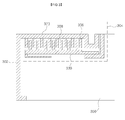
- Figure 1 illustrates the structure of a multi band internal antenna according to a first disclosed embodiment of the present invention.
- a multi band internal antenna can include a board 100, a radiation element 102 and an impedance matching/feeding part 104 formed on the board.
- the board 100 may be made of a dielectric material, and may serve as the antenna's main body, to which the other components may be joined.
- a variety of dielectric materials can be applied as the board 100.
- the board can be a PCB, FR4 board, etc.
- an antenna structured as an inverted-F antenna may utilize point matching with the radiation element by way of shorting pins, etc. This point matching, however, may narrow the frequency bandwidth.
- an embodiment of the present invention which uses a matching method based on coupling, and which includes an impedance matching/feeding part 104 having a particular length.
- the impedance matching/feeding part 104 may include a first matching element 120, which may be electrically coupled to a ground, and a second matching element 130, which may be electrically coupled to a feeding point (not shown). Coupling feeding may be performed within the impedance matching/feeding part 104 from the second matching element 130 to the first matching element 120, while signals may be radiated by the radiation element 102, which is electrically coupled to the first matching element 120.
- the first matching element 120 and the second matching element 130 may be formed with a particular gap in-between, and the interaction between the first matching element 120 and the second matching element may enable coupling matching.
- the capacitance component may play a greater role than the inductance component, and as such the present embodiment presents a structure that enables impedance matching for an wide-band by diversifying the capacitance component.
- the gap between the first matching element 120 and the second matching element 130 may be partially varied.
- Figure 1 An example of partially varying the distance between the first matching element 120 and the second matching element 130 is shown in Figure 1 , which illustrates a structure in which the first matching element 120 is bent several times, and the second matching element 130 is bent correspondingly.
- the first matching element 120 may be divided into three sections: section A1-A1', section A2-A2', and section A3-A3'.
- the second matching element 130 may be bent in correspondence with the first matching element 120, and may be divided into section B1-B1', section B2-B2', and section B3-B3'.
- the distance d1 between section A1-A1' and section B1-B1', the distance d2 between section A2-A2' and section B2-B2', and distance d3 between section A3-A3' and section B3-B3' are all different.
- first matching element 120 and the second matching element 130 as bending structures, and partially varying the distance in-between, wide-band characteristics by coupling matching and feeding can be obtained.
- Figure 1 illustrates an example in which the distance between the first matching element 120 and the second matching element 130 varies partially due to bends in the first matching element 120 and the second matching element 130, it will be understood by the skilled person that this may be implemented in a variety of ways other than that illustrated in Figure 1 .
- the second matching element 130 may be formed as a straight line, while the first matching element 120 and the radiation element may be arranged diagonally, so that the distance is made to vary.
- RF signals may be provide to the radiation element 102 by coupling feeding, as described above, and the radiation element 102 may radiate the signals to the exterior.
- the radiation element 102 may be connected to the first matching element 120 of the impedance matching/feeding part 104.
- the transmission frequency band may be determined by the length of the radiation element 102 and the length of the impedance matching/feeding part 104.
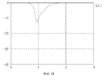
- Figure 2 represents S11 parameters of the antenna illustrated in Figure 1 .
- a structure which can both diversify the capacitance component and provide a high capacitance in certain regions. This can also reduce the impact of external factors such as the hand effect by high capacitance.
- Figure 3 illustrates the structure of a multi band internal antenna according to a second disclosed embodiment of the present invention.
- a multi band internal antenna may include a board 300, a radiation element 302 and an impedance matching/feeding part 304 formed on the board 300, where the impedance matching part 304 may include a first matching element 320 and a second matching element 330.
- first coupling elements 306 can be formed which protrude perpendicularly to the lengthwise direction of the first matching element 320
- second coupling elements 308 can be formed which protrude perpendicularly to the lengthwise direction of the second matching element.
- the first matching element 320 may be electrically coupled to a ground
- the second matching element 330 may be electrically coupled to a feeding point, and coupling feeding is performed from the second matching element 330 to the first matching element 320.
- the multi band internal antenna according to the second disclosed embodiment of the present invention is structured to allow coupling by a higher capacitance.
- the structure of the internal antenna according to the second disclosed embodiment of the present invention may include first coupling elements 306 and second coupling elements 308, in addition to the structure of an antenna according to the first disclosed embodiment.
- the first coupling elements 306 and second coupling elements 308 enable coupling matching by a higher capacitance.
- first coupling elements 306 and second coupling elements 308 may be formed protruding from the first matching element and second matching element in a comb-like form.
- first coupling elements 306 and the second coupling elements 308 may be formed alternately, to form generally comb-like shapes.
- These coupling elements 306, 308 may substantially narrow the distance between the first matching element and the second matching element, to not only provide a higher capacitance, but also aid in diversifying the capacitance component, so as to enable matching for wider bands.
- Figure 4 represents S11 parameters of a multi band antenna according to the second disclosed embodiment of the present invention.
- an antenna according to the second disclosed embodiment of the present invention exhibits wider band characteristics compared to the antenna of the first disclosed embodiment illustrated in Figure 2 .
- a structure for achieving greater coupling between the first matching element and the second matching element can be implemented in various ways other than by the structures illustrated in Figure 1 and Figure 3 .
- Figure 11 through Figure 13 are drawings that illustrate structures of first matching elements and second matching elements for obtaining greater coupling according to certain embodiments of the present invention.
- the widths and lengths of the coupling elements can be varied, and as shown in Figure 13 , the coupling elements can also be implemented in shapes other than rectangles.
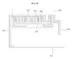
- Figure 5 illustrates the structure of a multi band internal antenna according to a third disclosed embodiment of the present invention.
- a multi band internal antenna may include a board 500, a first radiation element 502, an impedance matching/feeding part 504, and a second radiation element 506 formed on the board 500.
- the impedance matching/feeding part 504 may include a first matching element 520, which may be electrically coupled to a ground, and a second matching element 530, which may be electrically coupled to a feeding point, where coupling elements 306, 308 may be formed protruding from the first matching element 520 and second matching element to enable matching for wider bands.
- the first radiation element 502 may be formed extending from the first matching element 520 and feeding is performed by coupling.
- compositions of the first radiation element 502 and the impedance matching part 504 are substantially the same as those for the second disclosed embodiment described above, but the second radiation element 506 may be additionally included.
- the second radiation element 506 may be added for transmitting and receiving signals from different bands from those of the first radiation element 502.
- the second radiation element 506 may be separated by a particular distance from the first radiation element 502 and the impedance matching/feeding part 504 without electrical contact.
- the second radiation element 506 may be electrically coupled to a ground, and may receive power by coupling from the impedance matching/feeding part 504.
- Figure 5 illustrates an example in which the second radiation element 506 is shorter than the first radiation element 502, where the second radiation element 506 may be included to transmit and receive signals in a higher frequency band than that of the first radiation element 502.
- FIG. 5 illustrates the second radiation element 506 as having one bend, it will be apparent to the skilled person that the form of the second radiation element is not thus limited.
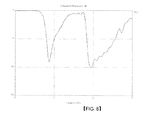
- Figure 6 represents S11 parameters of a multi band antenna according to the third disclosed embodiment of the present invention.
- Figure 7 illustrates the structure of multi band internal antenna according to a fourth disclosed embodiment of the present invention.
- a multi band internal antenna may include a board 700, and a first radiation element 702 formed on the board 700, an impedance matching/feeding part 704 formed on the board 700, and a second radiation element 706.
- the impedance matching/feeding part 704 may include a first matching element 720 and a second matching element 730, the first matching element 720 electrically coupled to a ground, and the second matching element 730 electrically coupled to a feeding point.
- the first radiation element may receive RF signals from the impedance matching/feeding part through coupling feeding.
- the second radiation element 706 does not receive power by coupling but by direct feeding.
- the second radiation element 706 may be electrically joined to the second matching element 730 of the impedance matching/feeding part 704, which is electrically coupled to a feeding point, so that direct feeding may be provided to the second radiation element 706.
- these radiation elements can be provided with power either by coupling, as in the third disclosed embodiment, or by direct power feeding, as in the fourth disclosed embodiment.
- Figure 7 illustrates an example in which the second matching element 730 and the second radiation element 706 are electrically joined on the board
- the second matching element 730 and the second radiation element 706 do not necessarily have to be joined on the board and can be electrically joined in another region.
- Figure 8 represents S11 parameters of a multi band antenna according to the fourth disclosed embodiment of the present invention.
- Figure 9 illustrates a structure in which a multi band internal antenna according to the third disclosed embodiment of the present invention is joined to an antenna carrier of a terminal.
- the antenna carrier may include a horizontal part 900 and a vertical part 902, where the vertical part 902 may be formed perpendicularly to the board 910 of the terminal to support the horizontal part 900, and the horizontal part 900 may be formed parallel to the board of the terminal, with the elements described above joined to the horizontal part 900.
- the first matching element may extend to the vertical part 902 and join a ground of the terminal's board 910
- the second matching element may extend and electrically connect with a feeding point.
- the second radiation element may extend to the vertical part 902 and join the ground of the terminal's board 910.
- Figure 10 illustrates a structure in which a multi band internal antenna according to the fourth disclosed embodiment of the present invention is joined to a PCB of a terminal.
- the second radiation element and the second matching element coupled to the feeding point may be electrically joined at point A, so that direct power feeding may be provided to the second radiation element.
Abstract
Description
- The present invention relates to an antenna, more particularly to a multi band internal antenna.
- In current mobile terminals, there is a demand not only for smaller sizes and lighter weight, but also for functions that allow a user access to mobile communication services of different frequency bands through a single terminal. That is, there is a demand for a terminal with which a user may simultaneously utilize signals of multiple bands as necessary, from among mobile communication services of various frequency bands, such as the CDMA service based on the 824∼894 MHz band and the PCS service based on the 1750∼1870 MHz band commercialized in Korea, the CDMA service based on the 832∼925 MHz band commercialized in Japan, the PCS service based on the 1850∼1990 MHz commercialized in the United States, the GSM service based on the 880∼960 MHz band commercialized in Europe and China, and the DCS service based on the 1710∼1880 MHz band commercialized in parts of Europe. Furthermore, there is a demand for a composite terminal that allows the use of services such as Bluetooth, ZigBee, wireless LAN, GPS, etc. In this type of terminal for using services of multiple bands, a multi-band antenna is needed, which can operate in two or more desired bands. The antennas generally used in mobile terminals include the helical antenna and the planar inverted-F antenna (PIFA).
- Here, the helical antenna is an external antenna that is secured to an upper end of a terminal, and is used together with a monopole antenna. In an arrangement in which a helical antenna and a monopole antenna are used together, extending the antenna from the main body of the terminal allows the antenna to operate as a monopole antenna, while retracting the antenna allows the antenna to operate as a λ/4 helical antenna. While this type of antenna has the advantage of high gain, its non-directivity results in undesirable SAR characteristics, which form the criteria for levels of electromagnetic radiation hazardous to the human body. Also, since the helical antenna is formed protruding outwards of the terminal, it is difficult to design the exterior of the terminal to be aesthetically pleasing and suitable for carrying, but a built-in structure for the helical antenna has not yet been researched.
- The inverted-F antenna is an antenna designed to have a low profile structure in order to overcome such drawbacks. The inverted-F antenna has directivity, and when current induction to the radiating part generates beams, a beam flux directed toward the ground surface may be re-induced to attenuate another beam flux directed toward the human body, thereby improving SAR characteristics as well as enhancing beam intensity induced to the radiating part. Also, the inverted-F antenna operates as a rectangular micro-strip antenna, in which the length of a rectangular plate-shaped radiating part is reduced in half, whereby a low profile structure may be realized.
- Because the inverted-F antenna has directive radiation characteristics, so that the intensity of beams directed toward the human body may be attenuated and the intensity of beams directed away from the human body may be intensified, a higher absorption rate of electromagnetic radiation can be obtained, compared to the helical antenna. However, the inverted-F antenna may have a narrow frequency bandwidth when it is designed to operate in multiple bands.
- The narrow frequency bandwidth obtained when designing the inverted-F antenna to operate in multiple bands is resultant of point matching, in which matching with a radiator occurs at a particular point.
- Thus, there is a demand for an antenna that maintains a low profile structure and overcomes the drawback of the inverted-F antenna of narrow band characteristics for more stable operation in multiple bands.
- To resolve the problems in prior art described above, an objective of the present invention is to provide a multi band internal antenna that exhibits wide-band characteristics even for multi-band designs.
- Another objective of the present invention is to provide a multi band le internal antenna that provides wide-band characteristics using matching by coupling.
- Still another objective of the present invention is to provide a multi band internal antenna that is less affected by external factors, such as the hand effect.
- Additional objectives of the present invention will be obvious from the embodiments described below.
- To achieve the objectives above, an aspect of the present provides an multi band internal antenna that includes: a board, an impedance matching/feeding part formed on the board, and a first radiation element joined to the impedance matching/feeding part, where the impedance matching/feeding part includes: a first matching element of a particular length that is coupled to a ground, and a second matching element of a particular length that is arranged with a distance from the first matching element and is electrically coupled to a feeding point. The distance between the first matching element and the second matching element may vary partially.
- The first matching element and the second matching element may perform impedance matching by way of coupling.
- The first matching element may have a structure that includes at least one bend, while the second matching element may be bent in correspondence to the bending structure of the first matching element.
- The first radiation element may extend from the first matching element of the impedance matching/feeding part and may receive power from the second matching element by coupling.
- The antenna can further include a second radiation element, which is formed on the board and electrically coupled to a ground, where the second radiation element may receive power from the second matching element of the impedance matching/feeding part by coupling.
- In another embodiment, the antenna can further include a second radiation element, which is formed on the board and electrically coupled to the second matching element of the impedance matching/feeding part to receive power.
- Another aspect of the present invention provides an multi band internal antenna that includes: a board, an impedance matching/feeding part formed on the board, and a first radiation element joined to the impedance matching/feeding part, where the impedance matching/feeding part includes: a first matching element of a particular length that is coupled to a ground, and a second matching element of a particular length that is arranged with a distance from the first matching element and is electrically coupled to a feeding point. At least one of the first matching element and the second matching element may include a multiple number of coupling elements that protrude from the first matching element or the second matching element.
- Certain aspects of the present invention can provide a multi band internal antenna that utilizes coupling matching to achieve wide-band characteristics even for multi-band designs. Also, certain aspects of the present invention can provide a multi band antenna that is less affected by external factors, such as the hand effect.
-
-
Figure 1 illustrates the structure of a multi band internal antenna according to a first disclosed embodiment of the present invention. -
Figure 2 represents S11 parameters of the antenna illustrated inFigure 1 . -
Figure 3 illustrates the structure of a multi band internal antenna according to a second disclosed embodiment of the present invention. -
Figure 4 represents S11 parameters of a multi band antenna according to the second disclosed embodiment of the present invention. -
Figure 5 illustrates the structure of a multi band internal antenna according to a third disclosed embodiment of the present invention. -
Figure 6 represents S11 parameters of an multi band antenna according to the third disclosed embodiment of the present invention. -
Figure 7 illustrates the structure of a multi band internal antenna according to a fourth disclosed embodiment of the present invention. -
Figure 8 represents S11 parameters of an multi band antenna according to the fourth disclosed embodiment of the present invention. -
Figure 9 illustrates a structure in which a multi band internal antenna according to the third disclosed embodiment of the present invention is joined to an antenna carrier of a terminal. -
Figure 10 illustrates a structure in which a multi band internal antenna according to the fourth disclosed embodiment of the present invention is joined to a PCB of a terminal. -
Figure 11 through Figure 13 illustrate structures of the first matching elements and second matching elements according to embodiments of the present invention that provide high coupling. - The multi band internal antenna according to certain embodiments of the present invention will be described below in more detail with reference to the accompanying drawings.
- The embodiments disclosed in the present specification will be presented using as an example a multi band antenna employed in GSM service bands, PCS service bands, and WCDMA service bands. However, the multi band internal antenna according to embodiments of the present invention is not limited to the above bands, and can be made to operate for various frequency bands.
-
Figure 1 illustrates the structure of a multi band internal antenna according to a first disclosed embodiment of the present invention. - Referring to
Figure 1 , a multi band internal antenna according to the first disclosed embodiment of the present invention can include aboard 100, aradiation element 102 and an impedance matching/feedingpart 104 formed on the board. - In
Figure 1 , theboard 100 may be made of a dielectric material, and may serve as the antenna's main body, to which the other components may be joined. A variety of dielectric materials can be applied as theboard 100. For example, the board can be a PCB, FR4 board, etc. - As described above, an antenna structured as an inverted-F antenna may utilize point matching with the radiation element by way of shorting pins, etc. This point matching, however, may narrow the frequency bandwidth.
- To resolve the drawback of point matching stated above, an embodiment of the present invention is presented which uses a matching method based on coupling, and which includes an impedance matching/feeding
part 104 having a particular length. - The impedance matching/
feeding part 104 may include a first matchingelement 120, which may be electrically coupled to a ground, and a second matchingelement 130, which may be electrically coupled to a feeding point (not shown). Coupling feeding may be performed within the impedance matching/feedingpart 104 from the second matchingelement 130 to thefirst matching element 120, while signals may be radiated by theradiation element 102, which is electrically coupled to thefirst matching element 120. - The
first matching element 120 and the second matchingelement 130 may be formed with a particular gap in-between, and the interaction between thefirst matching element 120 and the second matching element may enable coupling matching. In the interaction between thefirst matching element 120 and thesecond matching element 130, the capacitance component may play a greater role than the inductance component, and as such the present embodiment presents a structure that enables impedance matching for an wide-band by diversifying the capacitance component. - In order to diversify the capacitance component, the gap between the
first matching element 120 and thesecond matching element 130 may be partially varied. - An example of partially varying the distance between the
first matching element 120 and thesecond matching element 130 is shown inFigure 1 , which illustrates a structure in which thefirst matching element 120 is bent several times, and thesecond matching element 130 is bent correspondingly. - Based on the bending positions, the
first matching element 120 may be divided into three sections: section A1-A1', section A2-A2', and section A3-A3'. Thesecond matching element 130 may be bent in correspondence with thefirst matching element 120, and may be divided into section B1-B1', section B2-B2', and section B3-B3'. - In an embodiment of the present invention, the distance d1 between section A1-A1' and section B1-B1', the distance d2 between section A2-A2' and section B2-B2', and distance d3 between section A3-A3' and section B3-B3' are all different.
- Thus, by implementing the
first matching element 120 and thesecond matching element 130 as bending structures, and partially varying the distance in-between, wide-band characteristics by coupling matching and feeding can be obtained. - While
Figure 1 illustrates an example in which the distance between thefirst matching element 120 and thesecond matching element 130 varies partially due to bends in thefirst matching element 120 and thesecond matching element 130, it will be understood by the skilled person that this may be implemented in a variety of ways other than that illustrated inFigure 1 . - Various embodiments that include varying distance between the first matching element and the second matching element are encompassed within the scope of the present invention. In one embodiment, for example, the
second matching element 130 may be formed as a straight line, while thefirst matching element 120 and the radiation element may be arranged diagonally, so that the distance is made to vary. - RF signals may be provide to the
radiation element 102 by coupling feeding, as described above, and theradiation element 102 may radiate the signals to the exterior. Theradiation element 102 may be connected to thefirst matching element 120 of the impedance matching/feeding part 104. Here, the transmission frequency band may be determined by the length of theradiation element 102 and the length of the impedance matching/feeding part 104. -
Figure 2 represents S11 parameters of the antenna illustrated inFigure 1 . - Referring to
Figure 2 , it can be observed that the S11 parameters of the antenna illustrated inFigure 1 represent relatively wide band characteristics. - In order to obtain wider band characteristics when utilizing matching by coupling, a structure is desired which can both diversify the capacitance component and provide a high capacitance in certain regions. This can also reduce the impact of external factors such as the hand effect by high capacitance..
-
Figure 3 illustrates the structure of a multi band internal antenna according to a second disclosed embodiment of the present invention. - Referring to
Figure 3 , a multi band internal antenna according to the second disclosed embodiment of the present invention may include aboard 300, aradiation element 302 and an impedance matching/feeding part 304 formed on theboard 300, where theimpedance matching part 304 may include afirst matching element 320 and asecond matching element 330. - Also, a multiple number of
first coupling elements 306 can be formed which protrude perpendicularly to the lengthwise direction of thefirst matching element 320, and a multiple number ofsecond coupling elements 308 can be formed which protrude perpendicularly to the lengthwise direction of the second matching element. - As in the first disclosed embodiment described above, the
first matching element 320 may be electrically coupled to a ground, and thesecond matching element 330 may be electrically coupled to a feeding point, and coupling feeding is performed from thesecond matching element 330 to thefirst matching element 320. - The multi band internal antenna according to the second disclosed embodiment of the present invention, as illustrated in
Figure 3 , is structured to allow coupling by a higher capacitance. - The structure of the internal antenna according to the second disclosed embodiment of the present invention may include
first coupling elements 306 andsecond coupling elements 308, in addition to the structure of an antenna according to the first disclosed embodiment. - The
first coupling elements 306 andsecond coupling elements 308 enable coupling matching by a higher capacitance. - As illustrated in
Figure 3 , thefirst coupling elements 306 andsecond coupling elements 308 may be formed protruding from the first matching element and second matching element in a comb-like form. In certain embodiments, thefirst coupling elements 306 and thesecond coupling elements 308 may be formed alternately, to form generally comb-like shapes. - These
coupling elements -
Figure 4 represents S11 parameters of a multi band antenna according to the second disclosed embodiment of the present invention. - Referring to
Figure 4 , it can be observed that an antenna according to the second disclosed embodiment of the present invention exhibits wider band characteristics compared to the antenna of the first disclosed embodiment illustrated inFigure 2 . - A structure for achieving greater coupling between the first matching element and the second matching element can be implemented in various ways other than by the structures illustrated in
Figure 1 andFigure 3 .Figure 11 through Figure 13 are drawings that illustrate structures of first matching elements and second matching elements for obtaining greater coupling according to certain embodiments of the present invention. - As illustrated in
Figure 11 through Figure 13 , the widths and lengths of the coupling elements can be varied, and as shown inFigure 13 , the coupling elements can also be implemented in shapes other than rectangles. -
Figure 5 illustrates the structure of a multi band internal antenna according to a third disclosed embodiment of the present invention. - Referring to
Figure 5 , a multi band internal antenna according to the third disclosed embodiment of the present invention may include aboard 500, afirst radiation element 502, an impedance matching/feeding part 504, and asecond radiation element 506 formed on theboard 500. - The impedance matching/
feeding part 504 may include afirst matching element 520, which may be electrically coupled to a ground, and asecond matching element 530, which may be electrically coupled to a feeding point, wherecoupling elements first matching element 520 and second matching element to enable matching for wider bands. - The
first radiation element 502 may be formed extending from thefirst matching element 520 and feeding is performed by coupling. - In the third disclosed embodiment, the compositions of the
first radiation element 502 and theimpedance matching part 504 are substantially the same as those for the second disclosed embodiment described above, but thesecond radiation element 506 may be additionally included. Thesecond radiation element 506 may be added for transmitting and receiving signals from different bands from those of thefirst radiation element 502. Thesecond radiation element 506 may be separated by a particular distance from thefirst radiation element 502 and the impedance matching/feeding part 504 without electrical contact. Thesecond radiation element 506 may be electrically coupled to a ground, and may receive power by coupling from the impedance matching/feeding part 504. -
Figure 5 illustrates an example in which thesecond radiation element 506 is shorter than thefirst radiation element 502, where thesecond radiation element 506 may be included to transmit and receive signals in a higher frequency band than that of thefirst radiation element 502. - While
Figure 5 illustrates thesecond radiation element 506 as having one bend, it will be apparent to the skilled person that the form of the second radiation element is not thus limited. - It will be understood by the skilled person that the approach of including additional radiation elements to form resonance points in other bands can be applied not only to the second disclosed embodiment but also to the first disclosed embodiment.
-
Figure 6 represents S11 parameters of a multi band antenna according to the third disclosed embodiment of the present invention. - Referring to
Figure 6 , it can be observed that, due to the addition of a second radiation element, resonance points have been formed at high-frequency bands. Two resonance points have been formed at high-frequency bands, and the extra resonance point is caused by a parasitic component. -
Figure 7 illustrates the structure of multi band internal antenna according to a fourth disclosed embodiment of the present invention. - Referring to
Figure 7 , a multi band internal antenna according to the fourth disclosed embodiment of the present invention may include aboard 700, and afirst radiation element 702 formed on theboard 700, an impedance matching/feeding part 704 formed on theboard 700, and asecond radiation element 706. - The impedance matching/
feeding part 704 may include afirst matching element 720 and asecond matching element 730, thefirst matching element 720 electrically coupled to a ground, and thesecond matching element 730 electrically coupled to a feeding point. - Similar to the second and third disclosed embodiments, the first radiation element may receive RF signals from the impedance matching/feeding part through coupling feeding.
- In the fourth disclosed embodiment as compared to the third disclosed embodiment, the
second radiation element 706 does not receive power by coupling but by direct feeding. Thesecond radiation element 706 may be electrically joined to thesecond matching element 730 of the impedance matching/feeding part 704, which is electrically coupled to a feeding point, so that direct feeding may be provided to thesecond radiation element 706. - Thus, when there are additional radiation elements for transmitting and receiving signals in other bands, these radiation elements can be provided with power either by coupling, as in the third disclosed embodiment, or by direct power feeding, as in the fourth disclosed embodiment.
- While
Figure 7 illustrates an example in which thesecond matching element 730 and thesecond radiation element 706 are electrically joined on the board, thesecond matching element 730 and thesecond radiation element 706 do not necessarily have to be joined on the board and can be electrically joined in another region. - Also, it will be apparent to the skilled person that the approach of including additional radiation elements to form resonance points in other bands can be applied not only to the second disclosed embodiment but also to the first disclosed embodiment.
-
Figure 8 represents S11 parameters of a multi band antenna according to the fourth disclosed embodiment of the present invention. - Referring to
Figure 8 , it can be observed that resonance points have been formed at high-frequency bands. Unlike the third disclosed embodiment shown inFigure 6 , however, there is no extra resonance point caused by a parasitic component. -
Figure 9 illustrates a structure in which a multi band internal antenna according to the third disclosed embodiment of the present invention is joined to an antenna carrier of a terminal. - The antenna carrier may include a
horizontal part 900 and avertical part 902, where thevertical part 902 may be formed perpendicularly to theboard 910 of the terminal to support thehorizontal part 900, and thehorizontal part 900 may be formed parallel to the board of the terminal, with the elements described above joined to thehorizontal part 900. - In
Figure 9 , the first matching element may extend to thevertical part 902 and join a ground of the terminal'sboard 910, and the second matching element may extend and electrically connect with a feeding point. Also, in cases where the second radiation element is included, the second radiation element may extend to thevertical part 902 and join the ground of the terminal'sboard 910. -
Figure 10 illustrates a structure in which a multi band internal antenna according to the fourth disclosed embodiment of the present invention is joined to a PCB of a terminal. Referring toFigure 10 , the second radiation element and the second matching element coupled to the feeding point, according to the fourth disclosed embodiment, may be electrically joined at point A, so that direct power feeding may be provided to the second radiation element. - The embodiments of the present invention described in the above are for illustrative purposes only. It is to be appreciated that those of ordinary skill in the art can modify, alter, and make additions to the embodiments without departing from the spirit and scope of the present invention, and that such modification, alterations, and additions are encompassed in the appended claims.
Claims (15)
- A multi band internal antenna comprising:a board; an impedance matching/feeding part formed on the board; anda first radiation element joined to the impedance matching/feeding part, wherein the impedance matching/feeding part comprises:a first matching element having a particular length and coupled to a ground; anda second matching element having a particular length and arranged with a distance from the first matching element, the second matching element electrically coupled to a feeding point, and wherein the distance between the first matching element and the second matching element varies partially.
- The multi band internal antenna of claim 1, wherein the first matching element and the second matching element perform impedance matching by way of coupling.
- The multi band internal antenna of claim 1, wherein the first matching element has a structure including at least one bend, and the second matching element is bent in correspondence to the bending structure of the first matching element.
- The multi band internal antenna of claim 3, wherein the first radiation element extends from the first matching element of the impedance matching/feeding part and receives power from the second matching element by coupling.
- The multi band internal antenna of claim 4, further comprising:a second radiation element formed on the board and electrically coupled to a ground, the second radiation element receiving power from the second matching element of the impedance matching/feeding part by coupling.
- The multi band internal antenna of claim 4, further comprising:a second radiation element formed on the board, the second radiation element electrically coupled to the second matching element of the impedance matching/feeding part for feeding..
- A multi band internal antenna comprising:a board;an impedance matching/feeding part formed on the board; anda first radiation element joined to the impedance matching/feeding part,wherein the impedance matching/feeding part comprises:a first matching element having a particular length and coupled to a ground; anda second matching element having a particular length and arranged with a distance from the first matching element, the second matching element electrically coupled to a feeding point, and wherein at least one of the first matching element and the second matching element comprises a plurality of coupling elements protruding from the first matching element or the second matching element.
- The multi band internal antenna of claim 7, wherein the first matching element and the second matching element perform impedance matching by way of coupling.
- The multi band internal antenna of claim 8, wherein the plurality of coupling elements protrude perpendicularly from the first matching element and the second matching element to form a generally comb-like shape.
- The multi band internal antenna of claim 8, wherein coupling elements protruding from the first matching element and coupling elements protruding from the second matching element are formed alternately.
- The multi band internal antenna of claim 8, wherein coupling elements protruding from the first matching element and coupling elements protruding from the second matching element have partially varying protrusion intervals and protrusion lengths.
- The multi band internal antenna of claim 8, wherein a distance between the first matching element and the second matching element varies partially.
- The multi band internal antenna of claim 8, wherein the first radiation element extends from the first matching element of the impedance matching/feeding part and receives power from the second matching element by coupling.
- The multi band internal antenna of claim 8, further comprising:a second radiation element formed on the board and electrically coupled to a ground, the second radiation element receiving power from the second matching element of the impedance matching/feeding part by coupling.
- The multi band internal antenna of claim 8, further comprising:a second radiation element formed on the board, the second radiation element electrically coupled to the second matching element of the impedance matching/feeding part to receive power.
Applications Claiming Priority (2)
| Application Number | Priority Date | Filing Date | Title |
|---|---|---|---|
| KR20080002266 | 2008-01-08 | ||
| PCT/KR2009/000095 WO2009088231A2 (en) | 2008-01-08 | 2009-01-08 | Multi-band internal antenna |
Publications (3)
| Publication Number | Publication Date |
|---|---|
| EP2242144A2 true EP2242144A2 (en) | 2010-10-20 |
| EP2242144A4 EP2242144A4 (en) | 2013-11-06 |
| EP2242144B1 EP2242144B1 (en) | 2020-08-19 |
Family
ID=40853604
Family Applications (1)
| Application Number | Title | Priority Date | Filing Date |
|---|---|---|---|
| EP09700969.0A Active EP2242144B1 (en) | 2008-01-08 | 2009-01-08 | Multi-band internal antenna |
Country Status (6)
| Country | Link |
|---|---|
| US (1) | US8884836B2 (en) |
| EP (1) | EP2242144B1 (en) |
| JP (1) | JP5777885B2 (en) |
| KR (1) | KR100985476B1 (en) |
| CN (1) | CN101911388B (en) |
| WO (1) | WO2009088231A2 (en) |
Cited By (7)
| Publication number | Priority date | Publication date | Assignee | Title |
|---|---|---|---|---|
| EP2421093A1 (en) * | 2009-04-14 | 2012-02-22 | ACE Technologies Corporation | Wideband antenna using coupling matching |
| EP2375489A3 (en) * | 2010-04-09 | 2014-11-26 | Sony Mobile Communications AB | Mobile wireless terminal and antenna device |
| EP2851997A4 (en) * | 2013-01-06 | 2015-07-22 | Huawei Tech Co Ltd | Printed circuit board antenna and printed circuit board |
| EP2280447A4 (en) * | 2008-04-30 | 2016-03-16 | Ace tech corp | Broadband internal antenna using slow-wave structure |
| EP3001503A4 (en) * | 2014-03-13 | 2016-03-30 | Huawei Device Co Ltd | Antenna and terminal |
| EP2369675A4 (en) * | 2008-12-10 | 2017-06-28 | ACE Technologies Corporation | Internal antenna supporting wideband impedance matching |
| EP3706244A1 (en) * | 2019-03-05 | 2020-09-09 | Japan Aviation Electronics Industry, Limited | Antenna |
Families Citing this family (27)
| Publication number | Priority date | Publication date | Assignee | Title |
|---|---|---|---|---|
| KR101044615B1 (en) * | 2009-04-27 | 2011-06-29 | 주식회사 에이스테크놀로지 | Broadband antenna using an electrical loop typed signal line |
| KR101043270B1 (en) * | 2009-09-03 | 2011-06-21 | 주식회사 모비텍 | Internal antenna using interdigit coupling |
| JP2011061638A (en) * | 2009-09-11 | 2011-03-24 | Tdk Corp | Antenna device |
| KR101132616B1 (en) * | 2009-09-23 | 2012-04-06 | 주식회사 이엠따블유 | Planar inverted f antenna with double coupling and wireless communication terminal having the same |
| WO2011046368A2 (en) * | 2009-10-13 | 2011-04-21 | 주식회사 에이스테크놀로지 | Broadband built-in antenna using double electromagnetic coupling |
| KR101090114B1 (en) | 2010-01-08 | 2011-12-07 | 주식회사 에이스테크놀로지 | Wide-band Embedded Antenna Using Electromagnetic Coupling |
| KR101120864B1 (en) * | 2010-03-31 | 2012-03-16 | 주식회사 에이스앤파트너스 | Wide-band Embedded Antenna with Improved Impedance Matching Using Electromagnetic Coupling |
| KR101094537B1 (en) * | 2010-03-31 | 2011-12-19 | 주식회사 에이스앤파트너스 | Wide-band Embedded Antenna Using Spiral Electromagnetic Coupling |
| KR101092094B1 (en) * | 2010-05-13 | 2011-12-12 | 라디나 주식회사 | Wide-band Antenna Using Extended Ground |
| US8654020B2 (en) | 2010-08-25 | 2014-02-18 | Radina Co., Ltd | Antenna having capacitive element |
| CN102468531B (en) * | 2010-11-04 | 2015-05-06 | 广达电脑股份有限公司 | Multi-frequency antenna |
| KR101288159B1 (en) | 2010-11-29 | 2013-07-18 | 주식회사 에이스테크놀로지 | Internal Antenna attached to Terminal Housing |
| CN102760940B (en) * | 2011-04-29 | 2015-05-27 | 纬创资通股份有限公司 | Coupled antenna and electronic device provided with same |
| KR101634824B1 (en) * | 2011-05-16 | 2016-06-29 | 라디나 주식회사 | Inverted F Antenna Using Branch Capacitor |
| TWI487198B (en) | 2011-06-03 | 2015-06-01 | Wistron Neweb Corp | A multi-band antenna |
| CN102820523B (en) * | 2011-06-07 | 2016-03-23 | 启碁科技股份有限公司 | Multifrequency antenna |
| CN102891352B (en) * | 2011-07-19 | 2015-04-29 | 深圳市信维通信股份有限公司 | Antenna unit, antenna and antenna matching device with antenna unit |
| KR101832961B1 (en) * | 2011-10-05 | 2018-02-28 | 엘지전자 주식회사 | Mobile terminal |
| US9178270B2 (en) * | 2012-05-17 | 2015-11-03 | Futurewei Technologies, Inc. | Wireless communication device with a multiband antenna, and methods of making and using thereof |
| KR101438151B1 (en) * | 2013-07-22 | 2014-09-04 | 순천향대학교 산학협력단 | Broadband antenna for mobile phone |
| CN104347926B (en) | 2013-07-31 | 2017-04-19 | 华为终端有限公司 | Printed antenna and terminal equipment |
| CN103647145A (en) * | 2013-12-27 | 2014-03-19 | 禾邦电子(苏州)有限公司 | Broadband modularized antenna and antenna assembly with same |
| WO2016029404A1 (en) | 2014-08-28 | 2016-03-03 | 华为技术有限公司 | Antenna apparatus and device |
| WO2016065588A1 (en) * | 2014-10-30 | 2016-05-06 | 华为技术有限公司 | Antenna apparatus and wireless terminal |
| US9363794B1 (en) * | 2014-12-15 | 2016-06-07 | Motorola Solutions, Inc. | Hybrid antenna for portable radio communication devices |
| CN106876903B (en) * | 2017-04-10 | 2023-05-16 | 西安巨向导航科技有限公司 | Antenna |
| JP7369545B2 (en) * | 2019-05-24 | 2023-10-26 | 株式会社デンソーテン | antenna device |
Citations (4)
| Publication number | Priority date | Publication date | Assignee | Title |
|---|---|---|---|---|
| EP0814535A2 (en) * | 1996-06-19 | 1997-12-29 | Murata Manufacturing Co., Ltd. | Surface-mount antenna and a communication apparatus using the same |
| US5903240A (en) * | 1996-02-13 | 1999-05-11 | Murata Mfg. Co. Ltd | Surface mounting antenna and communication apparatus using the same antenna |
| WO2004057698A2 (en) * | 2002-12-17 | 2004-07-08 | Ethertronics, Inc. | Antennas with reduced space and improved performance |
| JP2004236273A (en) * | 2003-02-03 | 2004-08-19 | Matsushita Electric Ind Co Ltd | Antenna |
Family Cites Families (22)
| Publication number | Priority date | Publication date | Assignee | Title |
|---|---|---|---|---|
| US2867126A (en) * | 1956-08-31 | 1959-01-06 | Clark Equipment Co | Transmission |
| JPH07193417A (en) | 1993-12-27 | 1995-07-28 | Central Glass Co Ltd | Glass antenna |
| AU696840B2 (en) * | 1995-03-20 | 1998-09-17 | Minnesota Mining And Manufacturing Company | Dual frequency antenna with integral diplexer |
| JP3114605B2 (en) | 1996-02-14 | 2000-12-04 | 株式会社村田製作所 | Surface mount antenna and communication device using the same |
| TW423180B (en) | 1997-01-31 | 2001-02-21 | Terajima Fumitaka | Glass antenna device for an automobile |
| JP3700372B2 (en) | 1997-01-31 | 2005-09-28 | 旭硝子株式会社 | Glass antenna device for vehicle |
| WO2001024316A1 (en) | 1999-09-30 | 2001-04-05 | Murata Manufacturing Co., Ltd. | Surface-mount antenna and communication device with surface-mount antenna |
| US20010050643A1 (en) * | 2000-02-22 | 2001-12-13 | Igor Egorov | Small-size broad-band printed antenna with parasitic element |
| JP3468201B2 (en) * | 2000-03-30 | 2003-11-17 | 株式会社村田製作所 | Surface mount antenna, frequency adjustment setting method of multiple resonance thereof, and communication device equipped with surface mount antenna |
| JP3658639B2 (en) * | 2000-04-11 | 2005-06-08 | 株式会社村田製作所 | Surface mount type antenna and radio equipped with the antenna |
| US6337667B1 (en) * | 2000-11-09 | 2002-01-08 | Rangestar Wireless, Inc. | Multiband, single feed antenna |
| CN100346532C (en) | 2001-03-15 | 2007-10-31 | 松下电器产业株式会社 | Antenna apparatus |
| JP2003258527A (en) * | 2002-02-27 | 2003-09-12 | Toyota Central Res & Dev Lab Inc | Antenna |
| US6914562B2 (en) * | 2003-04-10 | 2005-07-05 | Avery Dennison Corporation | RFID tag using a surface insensitive antenna structure |
| DE602004019375D1 (en) * | 2003-06-09 | 2009-03-26 | Panasonic Corp | ANTENNA AND ELECTRONIC DEVICE |
| EP1912279B1 (en) * | 2003-06-12 | 2011-01-05 | Research In Motion Limited | Multiple-element antenna with electromagnetically coupled floating antenna element |
| FI120606B (en) * | 2003-10-20 | 2009-12-15 | Pulse Finland Oy | Internal multi-band antenna |
| US7317901B2 (en) * | 2004-02-09 | 2008-01-08 | Motorola, Inc. | Slotted multiple band antenna |
| KR100649495B1 (en) * | 2004-09-06 | 2006-11-24 | 삼성전기주식회사 | Antenna module and electric apparatus using the same |
| JP2006197254A (en) * | 2005-01-13 | 2006-07-27 | Sakae Riken Kogyo Co Ltd | Antenna for automobile |
| KR100787229B1 (en) * | 2005-02-04 | 2007-12-21 | 삼성전자주식회사 | Printed inverted F antenna for dual band operation |
| JP4578411B2 (en) * | 2005-07-22 | 2010-11-10 | ブラザー工業株式会社 | Antenna and wireless tag |
-
2009
- 2009-01-08 US US12/811,485 patent/US8884836B2/en active Active
- 2009-01-08 JP JP2010542166A patent/JP5777885B2/en not_active Expired - Fee Related
- 2009-01-08 CN CN200980101818.XA patent/CN101911388B/en not_active Expired - Fee Related
- 2009-01-08 WO PCT/KR2009/000095 patent/WO2009088231A2/en active Application Filing
- 2009-01-08 KR KR1020090001577A patent/KR100985476B1/en active IP Right Grant
- 2009-01-08 EP EP09700969.0A patent/EP2242144B1/en active Active
Patent Citations (4)
| Publication number | Priority date | Publication date | Assignee | Title |
|---|---|---|---|---|
| US5903240A (en) * | 1996-02-13 | 1999-05-11 | Murata Mfg. Co. Ltd | Surface mounting antenna and communication apparatus using the same antenna |
| EP0814535A2 (en) * | 1996-06-19 | 1997-12-29 | Murata Manufacturing Co., Ltd. | Surface-mount antenna and a communication apparatus using the same |
| WO2004057698A2 (en) * | 2002-12-17 | 2004-07-08 | Ethertronics, Inc. | Antennas with reduced space and improved performance |
| JP2004236273A (en) * | 2003-02-03 | 2004-08-19 | Matsushita Electric Ind Co Ltd | Antenna |
Non-Patent Citations (1)
| Title |
|---|
| See also references of WO2009088231A2 * |
Cited By (12)
| Publication number | Priority date | Publication date | Assignee | Title |
|---|---|---|---|---|
| EP2280447A4 (en) * | 2008-04-30 | 2016-03-16 | Ace tech corp | Broadband internal antenna using slow-wave structure |
| EP2369675A4 (en) * | 2008-12-10 | 2017-06-28 | ACE Technologies Corporation | Internal antenna supporting wideband impedance matching |
| EP2421093A1 (en) * | 2009-04-14 | 2012-02-22 | ACE Technologies Corporation | Wideband antenna using coupling matching |
| EP2421093A4 (en) * | 2009-04-14 | 2012-09-05 | Ace tech corp | Wideband antenna using coupling matching |
| EP2375489A3 (en) * | 2010-04-09 | 2014-11-26 | Sony Mobile Communications AB | Mobile wireless terminal and antenna device |
| EP2851997A4 (en) * | 2013-01-06 | 2015-07-22 | Huawei Tech Co Ltd | Printed circuit board antenna and printed circuit board |
| US9825366B2 (en) | 2013-01-06 | 2017-11-21 | Huawei Technologies Co., Ltd. | Printed circuit board antenna and printed circuit board |
| EP3001503A4 (en) * | 2014-03-13 | 2016-03-30 | Huawei Device Co Ltd | Antenna and terminal |
| EP3706244A1 (en) * | 2019-03-05 | 2020-09-09 | Japan Aviation Electronics Industry, Limited | Antenna |
| CN111668586A (en) * | 2019-03-05 | 2020-09-15 | 日本航空电子工业株式会社 | Antenna with a shield |
| US11101563B2 (en) | 2019-03-05 | 2021-08-24 | Japan Aviation Electronics Industry, Limited | Antenna |
| CN111668586B (en) * | 2019-03-05 | 2022-04-19 | 日本航空电子工业株式会社 | Antenna with a shield |
Also Published As
| Publication number | Publication date |
|---|---|
| JP2011509624A (en) | 2011-03-24 |
| WO2009088231A3 (en) | 2009-10-22 |
| EP2242144A4 (en) | 2013-11-06 |
| US20110181487A1 (en) | 2011-07-28 |
| CN101911388A (en) | 2010-12-08 |
| KR100985476B1 (en) | 2010-10-05 |
| EP2242144B1 (en) | 2020-08-19 |
| WO2009088231A2 (en) | 2009-07-16 |
| KR20090076839A (en) | 2009-07-13 |
| US8884836B2 (en) | 2014-11-11 |
| CN101911388B (en) | 2014-04-09 |
| JP5777885B2 (en) | 2015-09-09 |
Similar Documents
| Publication | Publication Date | Title |
|---|---|---|
| EP2242144A2 (en) | Multi-band internal antenna | |
| US8587494B2 (en) | Internal antenna providing impedance matching for multiband | |
| US8477073B2 (en) | Internal wide band antenna using slow wave structure | |
| EP2421093A1 (en) | Wideband antenna using coupling matching | |
| KR101103208B1 (en) | Broad Band Antenna of Which the Radiator End Point is Shorted Using Coupling Matching | |
| US20130016026A1 (en) | Broadband internal antenna using electromagnetic coupling supporting improved impedance matching | |
| KR101044615B1 (en) | Broadband antenna using an electrical loop typed signal line | |
| KR101129976B1 (en) | Internal Antenna Providing Impedance Matching for Wide Band where Feeding Patch is Placed on Substrate | |
| KR101090114B1 (en) | Wide-band Embedded Antenna Using Electromagnetic Coupling | |
| KR20100099076A (en) | Ultra wide band monopole internal antenna | |
| EP2369675A1 (en) | Internal antenna supporting wideband impedance matching | |
| KR101081397B1 (en) | Wide-band Embedded Antenna Using Double Electromagnetic Coupling | |
| KR20110120154A (en) | Wide-band embedded antenna | |
| KR101094537B1 (en) | Wide-band Embedded Antenna Using Spiral Electromagnetic Coupling | |
| KR101053105B1 (en) | Broadband Antenna Using Tubular Matching | |
| KR20110040127A (en) | Wideband impedance matching antenna using coupling |
Legal Events
| Date | Code | Title | Description |
|---|---|---|---|
| PUAI | Public reference made under article 153(3) epc to a published international application that has entered the european phase |
Free format text: ORIGINAL CODE: 0009012 |
|
| 17P | Request for examination filed |
Effective date: 20100701 |
|
| AK | Designated contracting states |
Kind code of ref document: A2 Designated state(s): AT BE BG CH CY CZ DE DK EE ES FI FR GB GR HR HU IE IS IT LI LT LU LV MC MK MT NL NO PL PT RO SE SI SK TR |
|
| AX | Request for extension of the european patent |
Extension state: AL BA RS |
|
| DAX | Request for extension of the european patent (deleted) | ||
| A4 | Supplementary search report drawn up and despatched |
Effective date: 20131007 |
|
| RIC1 | Information provided on ipc code assigned before grant |
Ipc: H01Q 5/00 20060101ALI20130930BHEP Ipc: H01Q 9/42 20060101ALI20130930BHEP Ipc: H01Q 1/36 20060101AFI20130930BHEP Ipc: H01Q 1/38 20060101ALI20130930BHEP |
|
| RAP1 | Party data changed (applicant data changed or rights of an application transferred) |
Owner name: ACE TECHNOLOGIES CORPORATION |
|
| STAA | Information on the status of an ep patent application or granted ep patent |
Free format text: STATUS: EXAMINATION IS IN PROGRESS |
|
| 17Q | First examination report despatched |
Effective date: 20170403 |
|
| REG | Reference to a national code |
Ref country code: DE Ref legal event code: R079 Ref document number: 602009062626 Country of ref document: DE Free format text: PREVIOUS MAIN CLASS: H01Q0005000000 Ipc: H01Q0005371000 |
|
| GRAP | Despatch of communication of intention to grant a patent |
Free format text: ORIGINAL CODE: EPIDOSNIGR1 |
|
| RIC1 | Information provided on ipc code assigned before grant |
Ipc: H01Q 5/50 20150101ALI20200320BHEP Ipc: H01Q 1/36 20060101ALI20200320BHEP Ipc: H01Q 1/38 20060101ALI20200320BHEP Ipc: H01Q 5/371 20150101AFI20200320BHEP Ipc: H01Q 9/42 20060101ALI20200320BHEP |
|
| STAA | Information on the status of an ep patent application or granted ep patent |
Free format text: STATUS: GRANT OF PATENT IS INTENDED |
|
| INTG | Intention to grant announced |
Effective date: 20200430 |
|
| GRAS | Grant fee paid |
Free format text: ORIGINAL CODE: EPIDOSNIGR3 |
|
| GRAA | (expected) grant |
Free format text: ORIGINAL CODE: 0009210 |
|
| STAA | Information on the status of an ep patent application or granted ep patent |
Free format text: STATUS: THE PATENT HAS BEEN GRANTED |
|
| AK | Designated contracting states |
Kind code of ref document: B1 Designated state(s): AT BE BG CH CY CZ DE DK EE ES FI FR GB GR HR HU IE IS IT LI LT LU LV MC MK MT NL NO PL PT RO SE SI SK TR |
|
| REG | Reference to a national code |
Ref country code: GB Ref legal event code: FG4D |
|
| REG | Reference to a national code |
Ref country code: CH Ref legal event code: EP |
|
| REG | Reference to a national code |
Ref country code: DE Ref legal event code: R096 Ref document number: 602009062626 Country of ref document: DE |
|
| REG | Reference to a national code |
Ref country code: AT Ref legal event code: REF Ref document number: 1305008 Country of ref document: AT Kind code of ref document: T Effective date: 20200915 |
|
| REG | Reference to a national code |
Ref country code: IE Ref legal event code: FG4D |
|
| REG | Reference to a national code |
Ref country code: LT Ref legal event code: MG4D |
|
| REG | Reference to a national code |
Ref country code: NL Ref legal event code: MP Effective date: 20200819 |
|
| PG25 | Lapsed in a contracting state [announced via postgrant information from national office to epo] |
Ref country code: GR Free format text: LAPSE BECAUSE OF FAILURE TO SUBMIT A TRANSLATION OF THE DESCRIPTION OR TO PAY THE FEE WITHIN THE PRESCRIBED TIME-LIMIT Effective date: 20201120 Ref country code: NO Free format text: LAPSE BECAUSE OF FAILURE TO SUBMIT A TRANSLATION OF THE DESCRIPTION OR TO PAY THE FEE WITHIN THE PRESCRIBED TIME-LIMIT Effective date: 20201119 Ref country code: PT Free format text: LAPSE BECAUSE OF FAILURE TO SUBMIT A TRANSLATION OF THE DESCRIPTION OR TO PAY THE FEE WITHIN THE PRESCRIBED TIME-LIMIT Effective date: 20201221 Ref country code: FI Free format text: LAPSE BECAUSE OF FAILURE TO SUBMIT A TRANSLATION OF THE DESCRIPTION OR TO PAY THE FEE WITHIN THE PRESCRIBED TIME-LIMIT Effective date: 20200819 Ref country code: SE Free format text: LAPSE BECAUSE OF FAILURE TO SUBMIT A TRANSLATION OF THE DESCRIPTION OR TO PAY THE FEE WITHIN THE PRESCRIBED TIME-LIMIT Effective date: 20200819 Ref country code: BG Free format text: LAPSE BECAUSE OF FAILURE TO SUBMIT A TRANSLATION OF THE DESCRIPTION OR TO PAY THE FEE WITHIN THE PRESCRIBED TIME-LIMIT Effective date: 20201119 Ref country code: HR Free format text: LAPSE BECAUSE OF FAILURE TO SUBMIT A TRANSLATION OF THE DESCRIPTION OR TO PAY THE FEE WITHIN THE PRESCRIBED TIME-LIMIT Effective date: 20200819 Ref country code: LT Free format text: LAPSE BECAUSE OF FAILURE TO SUBMIT A TRANSLATION OF THE DESCRIPTION OR TO PAY THE FEE WITHIN THE PRESCRIBED TIME-LIMIT Effective date: 20200819 |
|
| REG | Reference to a national code |
Ref country code: AT Ref legal event code: MK05 Ref document number: 1305008 Country of ref document: AT Kind code of ref document: T Effective date: 20200819 |
|
| PG25 | Lapsed in a contracting state [announced via postgrant information from national office to epo] |
Ref country code: IS Free format text: LAPSE BECAUSE OF FAILURE TO SUBMIT A TRANSLATION OF THE DESCRIPTION OR TO PAY THE FEE WITHIN THE PRESCRIBED TIME-LIMIT Effective date: 20201219 Ref country code: PL Free format text: LAPSE BECAUSE OF FAILURE TO SUBMIT A TRANSLATION OF THE DESCRIPTION OR TO PAY THE FEE WITHIN THE PRESCRIBED TIME-LIMIT Effective date: 20200819 Ref country code: NL Free format text: LAPSE BECAUSE OF FAILURE TO SUBMIT A TRANSLATION OF THE DESCRIPTION OR TO PAY THE FEE WITHIN THE PRESCRIBED TIME-LIMIT Effective date: 20200819 Ref country code: LV Free format text: LAPSE BECAUSE OF FAILURE TO SUBMIT A TRANSLATION OF THE DESCRIPTION OR TO PAY THE FEE WITHIN THE PRESCRIBED TIME-LIMIT Effective date: 20200819 |
|
| PG25 | Lapsed in a contracting state [announced via postgrant information from national office to epo] |
Ref country code: RO Free format text: LAPSE BECAUSE OF FAILURE TO SUBMIT A TRANSLATION OF THE DESCRIPTION OR TO PAY THE FEE WITHIN THE PRESCRIBED TIME-LIMIT Effective date: 20200819 Ref country code: EE Free format text: LAPSE BECAUSE OF FAILURE TO SUBMIT A TRANSLATION OF THE DESCRIPTION OR TO PAY THE FEE WITHIN THE PRESCRIBED TIME-LIMIT Effective date: 20200819 Ref country code: CZ Free format text: LAPSE BECAUSE OF FAILURE TO SUBMIT A TRANSLATION OF THE DESCRIPTION OR TO PAY THE FEE WITHIN THE PRESCRIBED TIME-LIMIT Effective date: 20200819 Ref country code: DK Free format text: LAPSE BECAUSE OF FAILURE TO SUBMIT A TRANSLATION OF THE DESCRIPTION OR TO PAY THE FEE WITHIN THE PRESCRIBED TIME-LIMIT Effective date: 20200819 |
|
| REG | Reference to a national code |
Ref country code: DE Ref legal event code: R097 Ref document number: 602009062626 Country of ref document: DE |
|
| PG25 | Lapsed in a contracting state [announced via postgrant information from national office to epo] |
Ref country code: AT Free format text: LAPSE BECAUSE OF FAILURE TO SUBMIT A TRANSLATION OF THE DESCRIPTION OR TO PAY THE FEE WITHIN THE PRESCRIBED TIME-LIMIT Effective date: 20200819 Ref country code: ES Free format text: LAPSE BECAUSE OF FAILURE TO SUBMIT A TRANSLATION OF THE DESCRIPTION OR TO PAY THE FEE WITHIN THE PRESCRIBED TIME-LIMIT Effective date: 20200819 |
|
| PLBE | No opposition filed within time limit |
Free format text: ORIGINAL CODE: 0009261 |
|
| STAA | Information on the status of an ep patent application or granted ep patent |
Free format text: STATUS: NO OPPOSITION FILED WITHIN TIME LIMIT |
|
| PG25 | Lapsed in a contracting state [announced via postgrant information from national office to epo] |
Ref country code: SK Free format text: LAPSE BECAUSE OF FAILURE TO SUBMIT A TRANSLATION OF THE DESCRIPTION OR TO PAY THE FEE WITHIN THE PRESCRIBED TIME-LIMIT Effective date: 20200819 |
|
| 26N | No opposition filed |
Effective date: 20210520 |
|
| PG25 | Lapsed in a contracting state [announced via postgrant information from national office to epo] |
Ref country code: IT Free format text: LAPSE BECAUSE OF FAILURE TO SUBMIT A TRANSLATION OF THE DESCRIPTION OR TO PAY THE FEE WITHIN THE PRESCRIBED TIME-LIMIT Effective date: 20200819 |
|
| REG | Reference to a national code |
Ref country code: DE Ref legal event code: R119 Ref document number: 602009062626 Country of ref document: DE |
|
| PG25 | Lapsed in a contracting state [announced via postgrant information from national office to epo] |
Ref country code: SI Free format text: LAPSE BECAUSE OF FAILURE TO SUBMIT A TRANSLATION OF THE DESCRIPTION OR TO PAY THE FEE WITHIN THE PRESCRIBED TIME-LIMIT Effective date: 20200819 Ref country code: MC Free format text: LAPSE BECAUSE OF FAILURE TO SUBMIT A TRANSLATION OF THE DESCRIPTION OR TO PAY THE FEE WITHIN THE PRESCRIBED TIME-LIMIT Effective date: 20200819 |
|
| REG | Reference to a national code |
Ref country code: CH Ref legal event code: PL |
|
| GBPC | Gb: european patent ceased through non-payment of renewal fee |
Effective date: 20210108 |
|
| PG25 | Lapsed in a contracting state [announced via postgrant information from national office to epo] |
Ref country code: LU Free format text: LAPSE BECAUSE OF NON-PAYMENT OF DUE FEES Effective date: 20210108 |
|
| REG | Reference to a national code |
Ref country code: BE Ref legal event code: MM Effective date: 20210131 |
|
| PG25 | Lapsed in a contracting state [announced via postgrant information from national office to epo] |
Ref country code: FR Free format text: LAPSE BECAUSE OF NON-PAYMENT OF DUE FEES Effective date: 20210131 |
|
| PG25 | Lapsed in a contracting state [announced via postgrant information from national office to epo] |
Ref country code: LI Free format text: LAPSE BECAUSE OF NON-PAYMENT OF DUE FEES Effective date: 20210131 Ref country code: GB Free format text: LAPSE BECAUSE OF NON-PAYMENT OF DUE FEES Effective date: 20210108 Ref country code: CH Free format text: LAPSE BECAUSE OF NON-PAYMENT OF DUE FEES Effective date: 20210131 Ref country code: DE Free format text: LAPSE BECAUSE OF NON-PAYMENT OF DUE FEES Effective date: 20210803 |
|
| PG25 | Lapsed in a contracting state [announced via postgrant information from national office to epo] |
Ref country code: IE Free format text: LAPSE BECAUSE OF NON-PAYMENT OF DUE FEES Effective date: 20210108 |
|
| PG25 | Lapsed in a contracting state [announced via postgrant information from national office to epo] |
Ref country code: IS Free format text: LAPSE BECAUSE OF FAILURE TO SUBMIT A TRANSLATION OF THE DESCRIPTION OR TO PAY THE FEE WITHIN THE PRESCRIBED TIME-LIMIT Effective date: 20201219 |
|
| PG25 | Lapsed in a contracting state [announced via postgrant information from national office to epo] |
Ref country code: BE Free format text: LAPSE BECAUSE OF NON-PAYMENT OF DUE FEES Effective date: 20210131 |
|
| PG25 | Lapsed in a contracting state [announced via postgrant information from national office to epo] |
Ref country code: HU Free format text: LAPSE BECAUSE OF FAILURE TO SUBMIT A TRANSLATION OF THE DESCRIPTION OR TO PAY THE FEE WITHIN THE PRESCRIBED TIME-LIMIT; INVALID AB INITIO Effective date: 20090108 Ref country code: CY Free format text: LAPSE BECAUSE OF FAILURE TO SUBMIT A TRANSLATION OF THE DESCRIPTION OR TO PAY THE FEE WITHIN THE PRESCRIBED TIME-LIMIT Effective date: 20200819 |
|
| PG25 | Lapsed in a contracting state [announced via postgrant information from national office to epo] |
Ref country code: MK Free format text: LAPSE BECAUSE OF FAILURE TO SUBMIT A TRANSLATION OF THE DESCRIPTION OR TO PAY THE FEE WITHIN THE PRESCRIBED TIME-LIMIT Effective date: 20200819 |