EP2242096A2 - Semiconductor device - Google Patents
Semiconductor device Download PDFInfo
- Publication number
- EP2242096A2 EP2242096A2 EP10004017A EP10004017A EP2242096A2 EP 2242096 A2 EP2242096 A2 EP 2242096A2 EP 10004017 A EP10004017 A EP 10004017A EP 10004017 A EP10004017 A EP 10004017A EP 2242096 A2 EP2242096 A2 EP 2242096A2
- Authority
- EP
- European Patent Office
- Prior art keywords
- pillar
- mos transistors
- diffusion layer
- shaped semiconductor
- layer
- Prior art date
- Legal status (The legal status is an assumption and is not a legal conclusion. Google has not performed a legal analysis and makes no representation as to the accuracy of the status listed.)
- Withdrawn
Links
Images






















Classifications
-
- H—ELECTRICITY
- H10—SEMICONDUCTOR DEVICES; ELECTRIC SOLID-STATE DEVICES NOT OTHERWISE PROVIDED FOR
- H10D—INORGANIC ELECTRIC SEMICONDUCTOR DEVICES
- H10D84/00—Integrated devices formed in or on semiconductor substrates that comprise only semiconducting layers, e.g. on Si wafers or on GaAs-on-Si wafers
- H10D84/01—Manufacture or treatment
- H10D84/0123—Integrating together multiple components covered by H10D12/00 or H10D30/00, e.g. integrating multiple IGBTs
- H10D84/0126—Integrating together multiple components covered by H10D12/00 or H10D30/00, e.g. integrating multiple IGBTs the components including insulated gates, e.g. IGFETs
- H10D84/0165—Integrating together multiple components covered by H10D12/00 or H10D30/00, e.g. integrating multiple IGBTs the components including insulated gates, e.g. IGFETs the components including complementary IGFETs, e.g. CMOS devices
- H10D84/0195—Integrating together multiple components covered by H10D12/00 or H10D30/00, e.g. integrating multiple IGBTs the components including insulated gates, e.g. IGFETs the components including complementary IGFETs, e.g. CMOS devices the components including vertical IGFETs
-
- H—ELECTRICITY
- H10—SEMICONDUCTOR DEVICES; ELECTRIC SOLID-STATE DEVICES NOT OTHERWISE PROVIDED FOR
- H10D—INORGANIC ELECTRIC SEMICONDUCTOR DEVICES
- H10D30/00—Field-effect transistors [FET]
- H10D30/60—Insulated-gate field-effect transistors [IGFET]
- H10D30/67—Thin-film transistors [TFT]
- H10D30/6728—Vertical TFTs
-
- H—ELECTRICITY
- H10—SEMICONDUCTOR DEVICES; ELECTRIC SOLID-STATE DEVICES NOT OTHERWISE PROVIDED FOR
- H10D—INORGANIC ELECTRIC SEMICONDUCTOR DEVICES
- H10D84/00—Integrated devices formed in or on semiconductor substrates that comprise only semiconducting layers, e.g. on Si wafers or on GaAs-on-Si wafers
- H10D84/01—Manufacture or treatment
- H10D84/0123—Integrating together multiple components covered by H10D12/00 or H10D30/00, e.g. integrating multiple IGBTs
- H10D84/0126—Integrating together multiple components covered by H10D12/00 or H10D30/00, e.g. integrating multiple IGBTs the components including insulated gates, e.g. IGFETs
- H10D84/0165—Integrating together multiple components covered by H10D12/00 or H10D30/00, e.g. integrating multiple IGBTs the components including insulated gates, e.g. IGFETs the components including complementary IGFETs, e.g. CMOS devices
- H10D84/0172—Manufacturing their gate conductors
-
- H—ELECTRICITY
- H10—SEMICONDUCTOR DEVICES; ELECTRIC SOLID-STATE DEVICES NOT OTHERWISE PROVIDED FOR
- H10D—INORGANIC ELECTRIC SEMICONDUCTOR DEVICES
- H10D84/00—Integrated devices formed in or on semiconductor substrates that comprise only semiconducting layers, e.g. on Si wafers or on GaAs-on-Si wafers
- H10D84/01—Manufacture or treatment
- H10D84/0123—Integrating together multiple components covered by H10D12/00 or H10D30/00, e.g. integrating multiple IGBTs
- H10D84/0126—Integrating together multiple components covered by H10D12/00 or H10D30/00, e.g. integrating multiple IGBTs the components including insulated gates, e.g. IGFETs
- H10D84/0165—Integrating together multiple components covered by H10D12/00 or H10D30/00, e.g. integrating multiple IGBTs the components including insulated gates, e.g. IGFETs the components including complementary IGFETs, e.g. CMOS devices
- H10D84/0188—Manufacturing their isolation regions
-
- H—ELECTRICITY
- H10—SEMICONDUCTOR DEVICES; ELECTRIC SOLID-STATE DEVICES NOT OTHERWISE PROVIDED FOR
- H10D—INORGANIC ELECTRIC SEMICONDUCTOR DEVICES
- H10D84/00—Integrated devices formed in or on semiconductor substrates that comprise only semiconducting layers, e.g. on Si wafers or on GaAs-on-Si wafers
- H10D84/01—Manufacture or treatment
- H10D84/02—Manufacture or treatment characterised by using material-based technologies
- H10D84/03—Manufacture or treatment characterised by using material-based technologies using Group IV technology, e.g. silicon technology or silicon-carbide [SiC] technology
- H10D84/038—Manufacture or treatment characterised by using material-based technologies using Group IV technology, e.g. silicon technology or silicon-carbide [SiC] technology using silicon technology, e.g. SiGe
-
- H—ELECTRICITY
- H10—SEMICONDUCTOR DEVICES; ELECTRIC SOLID-STATE DEVICES NOT OTHERWISE PROVIDED FOR
- H10D—INORGANIC ELECTRIC SEMICONDUCTOR DEVICES
- H10D84/00—Integrated devices formed in or on semiconductor substrates that comprise only semiconducting layers, e.g. on Si wafers or on GaAs-on-Si wafers
- H10D84/80—Integrated devices formed in or on semiconductor substrates that comprise only semiconducting layers, e.g. on Si wafers or on GaAs-on-Si wafers characterised by the integration of at least one component covered by groups H10D12/00 or H10D30/00, e.g. integration of IGFETs
- H10D84/82—Integrated devices formed in or on semiconductor substrates that comprise only semiconducting layers, e.g. on Si wafers or on GaAs-on-Si wafers characterised by the integration of at least one component covered by groups H10D12/00 or H10D30/00, e.g. integration of IGFETs of only field-effect components
- H10D84/83—Integrated devices formed in or on semiconductor substrates that comprise only semiconducting layers, e.g. on Si wafers or on GaAs-on-Si wafers characterised by the integration of at least one component covered by groups H10D12/00 or H10D30/00, e.g. integration of IGFETs of only field-effect components of only insulated-gate FETs [IGFET]
- H10D84/85—Complementary IGFETs, e.g. CMOS
-
- H—ELECTRICITY
- H10—SEMICONDUCTOR DEVICES; ELECTRIC SOLID-STATE DEVICES NOT OTHERWISE PROVIDED FOR
- H10D—INORGANIC ELECTRIC SEMICONDUCTOR DEVICES
- H10D86/00—Integrated devices formed in or on insulating or conducting substrates, e.g. formed in silicon-on-insulator [SOI] substrates or on stainless steel or glass substrates
- H10D86/01—Manufacture or treatment
-
- H—ELECTRICITY
- H10—SEMICONDUCTOR DEVICES; ELECTRIC SOLID-STATE DEVICES NOT OTHERWISE PROVIDED FOR
- H10D—INORGANIC ELECTRIC SEMICONDUCTOR DEVICES
- H10D86/00—Integrated devices formed in or on insulating or conducting substrates, e.g. formed in silicon-on-insulator [SOI] substrates or on stainless steel or glass substrates
- H10D86/201—Integrated devices formed in or on insulating or conducting substrates, e.g. formed in silicon-on-insulator [SOI] substrates or on stainless steel or glass substrates the substrates comprising an insulating layer on a semiconductor body, e.g. SOI
Definitions
- the present invention relates to a semiconductor device, and more particularly to an SGT (Surrounding Gate Transistor) which is a vertical MOS transistor comprising a pillar-shaped semiconductor layer having a sidewall serving as a channel region, and a gate electrode formed to surround the channel region.
- SGT Silicon Gate Transistor
- an SGT Square Gate Transistor
- a drain, a gate and a source are arranged in a vertical direction, so that an occupancy area can be significantly reduced as compared with a conventional planar transistor.
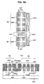
- FIG. 50(a) shows a top plan view of a CMOS inverter fabricated using the SGT disclosed in the Patent Document 1
- FIG. 50(b) is a sectional view taken along the cutting-plane line A-A' in the top plan view of FIG. 50(a) .
- an N-well 2502 and a P-well 2503 are formed in an upper region of a Si substrate 2501.
- a pillar-shaped silicon layer 2505 constituting a PMOS (PMOS pillar-shaped silicon layer 2505) and a pillar-shaped silicon layer 2506 constituting an NMOS (NMOS pillar-shaped silicon layer 2506) are formed on a surface of the Si substrate, specifically, on respective ones of the N-well region and the P-well region, and a gate 2508 is formed to surround the pillar-shaped silicon layers.
- a P + drain diffusion layer 2510 formed underneath the PMOS pillar-shaped silicon layer, and an N + drain diffusion layer 2512 formed underneath the NMOS pillar-shaped silicon layer, are connected to an output terminal Vout.
- a source diffusion layer 2509 formed on a top of the PMOS pillar-shaped silicon layer is connected to a power supply potential Vcc, and a source diffusion layer 2511 formed on a top of the NMOS pillar-shaped silicon layer is connected to a ground potential Vss.
- the common gate 2508 for the PMOS and the NMOS is connected to an input terminal Vin. In this manner, the CMOS inverter is formed.
- Patent Document 1 JP 2-188966A
- a logic circuit section requiring a high-speed operation is fabricated using a transistor having a minimum gate size L
- an I/O section for interfacing data communication with the outside is fabricated using a transistor having a longer gate length as compared with the transistor for the logic circuit section, because it is generally operated at an operating voltage greater than that for the logic circuit section.
- the transistor for the I/O section has a gate length about two or three times greater than that of the transistor for the logic circuit section.
- a transistor having a longer gate length as compared with the transistor for a typical logic circuit section is also used.
- due to a basic structure of an elemental or unit SGT it is difficult to form an SGT having a gate length greater than a gate length Ls of the unit SGT.
- a semiconductor device which comprises a first MOS transistor and a second MOS transistor each formed on a substrate, wherein each of the first and second MOS transistors is a vertical transistor in which a source diffusion layer, a drain diffusion layer and a pillar-shaped semiconductor layer are hierarchically arranged in a vertical direction with respect to the substrate while arranging the pillar-shaped semiconductor layer between the source diffusion layer and the drain diffusion layer, and a gate electrode is formed along a sidewall of the pillar-shaped semiconductor layer, and wherein: the first and second MOS transistors have a common gate electrode, and a common first planar diffusion layer formed on the substrate; the first MOS transistor has a first pillar-shaped diffusion layer formed on a top of the pillar-shaped semiconductor layer thereof to serve as the source diffusion layer; and the second MOS transistor has a second pillar-shaped diffusion layer formed on a top of the pillar-shaped semiconductor layer thereof to serve as the drain diffusion layer, and wherein the
- the semiconductor device includes a plurality of sets of the series-connected first and second MOS transistors, which are arranged in parallel, wherein the sets of series-connected first and second MOS transistors include a commonized gate electrode, a commonized source electrode and a commonized drain electrode.
- the vertical transistor for the first MOS transistor includes a plurality of the pillar-shaped semiconductor layers
- the vertical transistor for the second MOS transistor includes a plurality of the pillar-shaped semiconductor layers
- the first MOS transistor has a first gate electrode
- the second MOS transistor has a second gate electrode
- the first and second gate electrodes are connected to an interconnection layer via respective different contacts, so that they are interconnected together through the interconnection layer.
- each of the first and second gate electrodes may be connected to the interconnection layer via a plurality of contacts positioned at opposite ends thereof.
- a semiconductor device which comprises a first MOS transistor, a second MOS transistor and a third MOS transistor each formed on a substrate, wherein each of the first to third MOS transistors is a vertical transistor in which a source diffusion layer, a drain diffusion layer and a pillar-shaped semiconductor layer are hierarchically arranged in a vertical direction with respect to the substrate while arranging the pillar-shaped semiconductor layer between the source diffusion layer and the drain diffusion layer, and a gate electrode is formed along a sidewall of the pillar-shaped semiconductor layer, and wherein: the first to third MOS transistors have a common gate electrode; the first and second MOS transistors have a common first planar diffusion layer formed on the substrate; the third MOS transistor has a second planar diffusion layer formed on the substrate to serve as the drain diffusion layer; each of the second and third MOS transistors has a pillar-shaped diffusion layer formed on a top of the pillar-shaped semiconductor layer thereof, wherein the pillar-shaped diffusion layers of the
- the composite MOS transistor is formed by arranging in parallel a plurality of sets of the series-connected first to third MOS transistors having a gate electrode length three times greater than that of each of the first to third MOS transistors, and wherein the composite MOS transistor is configured to have a commonized gate electrode, a commonized source electrode and a commonized drain electrode to enhance a drive current.
- the vertical transistor for each of the first to third MOS transistors includes a plurality of the pillar-shaped semiconductor layers, and wherein: the first MOS transistor has a first gate electrode; the second MOS transistor has a second gate electrode; and the third MOS transistor has a third gate electrode, and wherein the first to third gate electrodes are connected to an interconnection layer via respective different contacts, so that they are interconnected together through the interconnection layer.
- each of the first to third gate electrodes may be connected to the interconnection layer via a plurality of contacts positioned at opposite ends thereof.
- a semiconductor device which comprises a first MOS transistor, a second MOS transistor, a third MOS transistor and a fourth MOS transistor each formed on a substrate, wherein each of the first to fourth MOS transistors is a vertical transistor in which a source diffusion layer, a drain diffusion layer and a pillar-shaped semiconductor layer are hierarchically arranged in a vertical direction with respect to the substrate while arranging the pillar-shaped semiconductor layer between the source diffusion layer and the drain diffusion layer, and a gate electrode is formed along a sidewall of the pillar-shaped semiconductor layer, and wherein: the first to fourth MOS transistors have a common gate electrode; the first and second MOS transistors have a common first planar diffusion layer formed on the substrate; the third and fourth MOS transistors have a common second planar diffusion layer formed on the substrate; each of the second and third MOS transistors has a pillar-shaped diffusion layer formed on a top of the pillar-shaped semiconductor layer thereof, wherein the pillar-shaped
- the composite MOS transistor is formed by arranging in parallel a plurality of sets of the series-connected first to fourth MOS transistors having a gate electrode length four times greater than that of each of the first to fourth MOS transistors, and wherein the composite MOS transistor is configured to have a commonized gate electrode, a commonized source electrode and a commonized drain electrode to enhance a drive current.
- the semiconductor device according the third aspect of the present invention comprises a contact formed on the gate electrode or each of the gate electrodes at a position corresponding to an element isolation region between the first and second planar diffusion layers.
- the vertical transistor for each of the first to fourth MOS transistors includes a plurality of the pillar-shaped semiconductor layers, and wherein: the first MOS transistor has a first gate electrode; the second MOS transistor has a second gate electrode; the third MOS transistor has a third gate electrode; and the fourth MOS transistor has a fourth gate electrode, and wherein the first to fourth gate electrodes are connected to an interconnection layer via respective different contacts, so that they are interconnected together through the interconnection layer.
- each of the first to fourth gate electrodes may be connected to the interconnection layer via a plurality of contacts positioned at opposite ends thereof.
- a semiconductor device operable as an inverter which comprises a first MOS transistor, a second MOS transistor, a third MOS transistor and a fourth MOS transistor each formed on a substrate, wherein each of the first to fourth MOS transistors is a vertical transistor in which a source diffusion layer, a drain diffusion layer and a pillar-shaped semiconductor layer are hierarchically arranged in a vertical direction with respect to the substrate while arranging the pillar-shaped semiconductor layer between the source diffusion layer and the drain diffusion layer, and a gate electrode is formed along a sidewall of the pillar-shaped semiconductor layer, and wherein: the first to fourth MOS transistors have a common gate electrode serving as an input terminal; the first and second MOS transistors have a common first planar diffusion layer formed on the substrate; the third and fourth MOS transistors have a common second planar diffusion layer formed on the substrate; the first MOS transistor has a pillar-shaped diffusion layer formed on a top of the pillar-shaped semiconductor layer thereof and
- each of the first and second MOS transistors may be an NMOS transistor, and each of the third and fourth MOS transistors may be a PMOS transistor.
- the inverter is formed by arranging in parallel a plurality of sets of the two composite MOS transistors comprising the first to forth MOS transistors and each having a gate electrode length two times greater than that of each of the first to fourth MOS transistors, and wherein the inverter is configured to have a commonized gate electrode, a commonized source electrode and a commonized drain electrode to enhance a drive current.
- the vertical transistor for each of the first to fourth MOS transistors includes a plurality of the pillar-shaped semiconductor layers, and wherein; the first and second MOS transistors have a common first gate electrode; and the third and fourth MOS transistors have a common second gate electrode, and wherein the first and second gate electrodes are connected to an interconnection layer via respective different contacts, so that they are interconnected together through the interconnection layer.
- the above semiconductor device comprises a contact formed on each of the first and second gate electrodes at a position corresponding to an element isolation region between the first and second planar diffusion layers.
- each of the first and second gate electrodes may be connected to the interconnection layer via a plurality of contacts positioned at opposite ends thereof.
- a semiconductor device operable as an inverter which comprises a first MOS transistor, a second MOS transistor, a third MOS transistor, a fourth MOS transistor, a fifth MOS transistor and a sixth MOS transistor each formed on a substrate
- each of the first to sixth MOS transistors is a vertical transistor in which a source diffusion layer, a drain diffusion layer and a pillar-shaped semiconductor layer are hierarchically arranged in a vertical direction with respect to the substrate while arranging the pillar-shaped semiconductor layer between the source diffusion layer and the drain diffusion layer, and a gate electrode is formed along a sidewall of the pillar-shaped semiconductor layer
- the first to sixth MOS transistors have a common gate electrode serving as an input terminal
- the first and second MOS transistors have a common first planar diffusion layer formed on the substrate
- the third MOS transistor has a second planar diffusion layer formed on the substrate
- the fourth and fifth MOS transistors have a common third planar diffusion layer formed on
- each of the first to third MOS transistors may be an NMOS transistor, and each of the fourth to sixth MOS transistors may be a PMOS transistor.
- the second and fourth planar diffusion layers are connected to each other through a silicide layer formed on respective surfaces thereof.
- the contact connected to the output terminal is formed on a boundary region between the second and fourth planar diffusion layers.
- the inverter is formed by arranging in parallel a plurality of sets of the two composite MOS transistors comprising the first to sixth MOS transistors and each having a gate electrode length three times greater than that of each of the first to sixth MOS transistors, and wherein the inverter is configured to have a commonized gate electrode, a commonized source electrode and a commonized drain electrode to enhance a drive current.
- the vertical transistor for each of the first to sixth MOS transistors includes a plurality of the pillar-shaped semiconductor layers, and wherein: the first and fourth MOS transistors have a common first gate electrode; and the second, third, fifth and sixth MOS transistors have a common second gate electrode, and wherein the first and second gate electrodes are connected to an interconnection layer via respective different contacts, so that they are interconnected together through the interconnection layer.
- a semiconductor device operable as an inverter which comprises a first MOS transistor, a second MOS transistor, a third MOS transistor, a fourth MOS transistor, a fifth MOS transistor, a sixth MOS transistor, a seventh MOS transistor and an eighth MOS transistor each formed on a substrate
- each of the first to eighth MOS transistors is a vertical transistor in which a source diffusion layer, a drain diffusion layer and a pillar-shaped semiconductor layer are hierarchically arranged in a vertical direction with respect to the substrate while arranging the pillar-shaped semiconductor layer between the source diffusion layer and the drain diffusion layer, and a gate electrode is formed along a sidewall of the pillar-shaped semiconductor layer
- the first to eighth MOS transistors have a common gate electrode serving as an input terminal
- the first and second MOS transistors have a common first planar diffusion layer formed on the substrate
- the third and fourth MOS transistors have a common second planar diffusion layer formed on the substrate
- the fifth MOS transistors having a common gate electrode serving as an input
- each of the first to fourth MOS transistors may be an NMOS transistor, and each of the fifth to eighth MOS transistors may be a PMOS transistor.
- the first and fifth MOS transistors have a common first gate electrode; the second and sixth MOS transistors have a common second gate electrode; the third and seventh MOS transistors have a common third gate electrode; and the fourth and eighth MOS transistors have a common fourth gate electrode, and wherein the first to fourth gate electrodes are connected to an interconnection layer via respective different contacts, so that they are interconnected together through the interconnection layer.
- each of the first to eighth MOS transistors includes a plurality of the pillar-shaped semiconductor layers.
- the contact on each of the first and second electrodes is formed on a boundary region defined between the first and third planar diffusion layers
- the contact on each of the third and fourth electrodes is formed on a boundary region defined between the second and fourth planar diffusion layers.
- the second, third, sixth and seventh MOS transistors have a common fifth gate electrode
- the first, fourth, fifth and eighth MOS transistors have a common sixth gate electrode
- the fifth and sixth gate electrodes are connected to an interconnection layer via respective different contacts, so that they are interconnected together through the interconnection layer.
- each of the first to eighth MOS transistors includes a plurality of the pillar-shaped semiconductor layers
- a semiconductor device operable as an inverter which comprises 1st to nth MOS transistors (wherein n is an integer of three or more) each formed on a substrate, wherein each of the 1st to nth MOS transistors is a vertical transistor in which a source diffusion layer, a drain diffusion layer and a pillar-shaped semiconductor layer are hierarchically arranged in a vertical direction with respect to the substrate while arranging the pillar-shaped semiconductor layer between the source diffusion layer and the drain diffusion layer, and a gate electrode is formed along a sidewall of the pillar-shaped semiconductor layer, and wherein: the 1st to nth MOS transistors have a common gate electrode; one of an upper portion and a lower portion of the pillar-shaped semiconductor layer in each of the 1st and nth MOS transistors is connected to one of an upper portion and a lower portion of the pillar-shaped semiconductor layer in an adjacent one of the remaining MOS transistors; and an upper portion and a
- a semiconductor device operable as a CMOS inverter which comprises 1st to nth NMOS transistors and 1st to nth PMOS transistors (wherein n is an integer of three or more), wherein: the 1st to nth NMOS transistors are formed on a substrate; each of the 1st to nth NMOS transistors is a vertical transistor in which a source diffusion layer, a drain diffusion layer and a pillar-shaped semiconductor layer are hierarchically arranged in a vertical direction with respect to the substrate while arranging the pillar-shaped semiconductor layer between the source diffusion layer and the drain diffusion layer, and a gate electrode is formed along a sidewall of the pillar-shaped semiconductor layer; the 1st to nth NMOS transistors have a common gate electrode serving as an input terminal; one of an upper portion and a lower portion of the pillar-shaped semiconductor layer in each of the 1st and nth NMOS transistors is connected to one of an
- the present invention makes it possible to design a composite SGT having a gate length greater than the minimum gate length of the unit SGT, and a circuit using the composite SGT.
- FIG. 1(a) is a top plan view showing a composite NMOS SGT having a gate length of 2Ls, according to a first embodiment of the present invention
- FIG. 1(b) is a sectional view taken along the cutting-plane line A-A' in FIG. 1(a) .
- the composite NMOS SGT having a gate length of 2Ls will be described below.
- a planar silicon layer 102 is formed on a buried oxide film layer 101, and two pillar-shaped silicon layers 105a, 105b are formed on the planar silicon layer 102.
- An N + lower diffusion layer 103 is formed in the planar silicon layer 102 underneath the pillar-shaped silicon layers 105a, 105b.
- a gate dielectric film 107 and a gate electrode 108 are formed around the pillar-shaped silicon layers 105a, 105b.
- the gate electrode 108 is connected to an interconnection layer 122 via a contact 117.
- An N + source diffusion layer 109a is formed in an upper portion of the pillar-shaped silicon layer 105a, and connected to an interconnection layer 120 serving as a source electrode, via a contact 115.
- An N + source diffusion layer 109b is formed in an upper portion of the pillar-shaped silicon layer 105b, and connected to an interconnection layer 121 serving as a drain electrode, via a contact 116.
- a first unit SGT comprising the pillar-shaped silicon layer 105a is connected in series with a second unit SGT comprising the pillar-shaped silicon layer 105b.
- the composite SGT operates as an SGT substantially having a gate length of 2Ls.
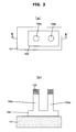
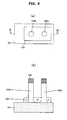
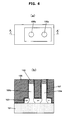
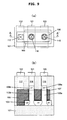
- FIGS. 2(a) to 9(b) one example of a production method for forming the composite SGT according to the first embodiment will be described.
- the figure suffixed with (a) is a top plan view
- the figure suffixed with (b) is a sectional view taken along the cutting-plane line A-A' in the top plan view of the figure suffixed with (a).
- a silicon nitride film 130 serving as a hard mask is formed on a silicon layer on a buried oxide film layer 101, and the hard mask 130 and the silicon layer are etched to form two pillar-shaped silicon layers 105a, 105b.
- the etching is performed to form a planar silicon layer 102 underneath the pillar-shaped silicon layers 105a, 105b.
- planar silicon layer 102 is etched to form an element isolation region therein.
- an impurity such as phosphorus (P) or arsenic (As)
- P phosphorus
- As arsenic
- the silicon nitride film 130 on a top of each of the pillar-shaped silicon layers functions as a stopper for preventing the impurity from being implanted into an upper portion of the pillar-shaped silicon layer.
- a gate dielectric film 107 and a gate conductive film 108 are formed.
- a thickness of the gate dielectric film may be increased as compared with cases where it is used in a logic circuit section.
- the gate conductive film 108 and the gate dielectric film 107 located above the pillar-shaped silicon layers are polished by chemical mechanical polishing (CMP), to flatten a top surface of the gate conductive film.
- CMP chemical mechanical polishing
- the flattening of the top surface of the gate conductive film by CMP makes it possible to improve a configuration of the gate conductive film to facilitate control of a gate length.
- the silicon nitride film 130 on the top of each of the pillar-shaped silicon layers is used as a CMP stopper.
- the use of the silicon nitride film 130 as a CMP stopper makes it possible to control an amount of CMP with high repeatability.
- the gate conductive film 108 is etched back in such a manner that the gate conductive film 108 is formed to have a desired gate length, i.e., a gate length is set.
- the silicon nitride film 130 as a hard mask is removed by etching, and then a gate electrode 108 is formed by lithography and dry etching. Subsequently, an impurity, such P or As, is introduced into an upper portion of each of the pillar-shaped silicon layers 105a, 105b by impurity implantation or the like, to form an N + source/drain diffusion layer (109a, 109b) therein.
- an impurity such P or As
- an interlayer dielectric film is formed, three contacts 115, 116, 117 are formed on the source/drain diffusion layer on the pillar-shaped silicon layer 105a, the source/drain diffusion layer on the pillar-shaped silicon layer 105b and the gate electrode, respectively. Then, three interconnection layers 120, 121, 122 are formed.
- FIG. 10 is a top plan view showing a composite NMOS SGT which is formed by connecting in parallel a plurality of sets of series-connected two unit SGTs, to having a gate length of 2Ls, according to a second embodiment of the present invention.
- a plurality of composite SGTs each fabricated as shown in FIGS. 1(a) and 1(b) to have a gate length of 2Ls are connected in parallel so as to form a transistor having a large drive current.
- a silicon layer 202 are formed on a buried oxide layer 201 in parallel with each other with respect to a row direction.
- a plurality of (e.g., five) sets of series-connected two pillar-shaped silicon layers 205a, 205b are formed on respective ones of the planar silicon layers 202, and an N + lower diffusion layer 203 is formed in each of the planar silicon layers 202 underneath the pillar-shaped silicon layers 205a, 205b.
- a gate electrode 208 is commonly formed around each of the sets of the series-connected pillar-shaped silicon layers 205a, 205b through a gate dielectric film.
- Each of the gate electrodes 208 is connected to an interconnection layer 222 via a contact 217.
- An N + upper diffusion layer is formed in an upper portion of each of the pillar-shaped silicon layers 205a, and connected to an interconnection layer 220 serving as a source electrode, via a contact 215 formed thereon.
- An N + upper diffusion layer is formed in an upper portion of each of the pillar-shaped silicon layers 205b, and connected to an interconnection layer 221 serving as a drain electrode, via a contact 216 formed thereon.
- FIG. 11 is a top plan view showing an example of modification of the composite NMOS SGT which is formed by connecting in parallel a plurality of sets of series-connected two unit SGTs, to have a gate length of 2Ls.
- a layout in FIG. 11 is different from that in FIG. 10 , in terms of a technique of gate interconnection.
- the number of contacts to be formed on the gate electrodes is increased by just an increase in the number of the sets of series-connected two unit SGTs to be connected in parallel.
- the layout illustrated in FIG. 11 even if the number of the sets of series-connected two unit SGTs to be connected in parallel is increased, the number of contacts to be formed on the gate electrodes is never increased, so that a transistor occupancy area is reduced accordingly.
- a planar silicon layer 302 is formed on a buried oxide layer 301.
- a plurality of (e.g., five) sets of series-connected two pillar-shaped silicon layers 305a, 305b are formed on the planar silicon layer 302 in parallel with each other with respect to a row direction, and an N + lower diffusion layer 303 is formed in the planar silicon layer 302 underneath the sets of pillar-shaped silicon layers 305a, 305b.
- a gate electrode 308b is commonly formed around a group of the plurality of pillar-shaped silicon layers 305b aligned in a column direction, through a gate dielectric film.
- Each of the gate electrodes 308a, 308b is connected to an interconnection layer 322 via a contact 317.
- An N + upper diffusion layer is formed in an upper portion of each of the pillar-shaped silicon layers 305a, and connected to an interconnection layer 320 serving as a source electrode, via a contact 315 formed thereon.
- An N + upper diffusion layer is formed in an upper portion of each of the pillar-shaped silicon layers 305b, and connected to an interconnection layer 321 serving as a drain electrode, via a contact 316 formed thereon.
- the contact 317 for each of the gate electrodes is formed at each of opposite ends of a respective one of the two columns of unit SGTs to be connected in parallel.
- the contact may be formed on only one of the ends.
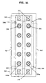
- FIG. 12(a) is a top plan view showing a composite NMOS SGT having a gate length of 3Ls, according to a third embodiment of the present invention
- FIG. 12(b) is a sectional view taken along the cutting-plane line A-A' in FIG. 12(a) .
- the composite NMOS SGT having a gate length of 3Ls will be described below.
- a first planar silicon layer 402a and a second planar silicon layer 402b are formed on a buried oxide film layer 401.
- a pillar-shaped silicon layer 405a is formed on the first planar silicon layer 402a, and two pillar-shaped silicon layers 405b, 405c are formed on the second planar silicon layer 402b.
- An N + lower diffusion layer 403a is formed in the first planar silicon layer 402a, and an N + lower diffusion layer 403b is formed in the second planar silicon layer 402b.
- a gate dielectric film 407 and a gate electrode 408 are formed around the pillar-shaped silicon layers 405a, 405b, 405c.
- the pillar-shaped silicon layers 405a, 405b, 405c are connected in series through an interconnection layer 423 and the lower diffusion layer 403b.
- the gate electrode 408 is connected to an interconnection layer 422 via a contact 417, and an interconnection layer 420 serving as a source electrode is connected to the lower diffusion layer 403a via a contact 415.
- a contact 416 formed on an upper diffusion layer 409c of the pillar-shaped silicon layer 405c is connected to an interconnection layer 421 serving as a drain electrode. Depending on an operating state, the relationship between the source and drain electrodes may be reversed.
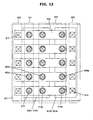
- FIG. 13 is a top plan view showing a composite NMOS SGT which is formed by connecting in parallel a plurality of sets of series-connected three unit SGTs, to have a gate length of 3Ls, according to a fourth embodiment of the present invention.
- a plurality of the composite SGTs each fabricated as shown in FIGS. 12(a) and 12(b) to have a gate length of 3Ls are connected in parallel so as to form a transistor having a large drive current.
- a first planar silicon layer 502a and a second planar silicon layer 502b are formed on a buried oxide film layer 501 along a row direction.
- a plurality of (e.g., five) pillar-shaped silicon layers 505a are formed on the first planar silicon layer 502a along a column direction.
- a plurality of (e.g., five) pillar-shaped silicon layers 505b and a plurality of (e.g., five) pillar-shaped silicon layers 505c are formed on the second planar silicon layer 502b in parallel with each other with respect to a column direction.
- N + lower diffusion layer 503a is formed in the first planar silicon layer 502a, and an N + lower diffusion layer 503b is formed in the second planar silicon layer 502b.
- a gate electrode 508 is commonly formed around each of a plurality of (e.g., five) sets of three pillar-shaped silicon layers 505a, 505b, 505c aligned in the row direction, through a gate dielectric film.
- Each of the sets of three pillar-shaped silicon layers 505a, 505b, 505c are connected in series through an interconnection layer 523 and the lower diffusion layer 503b.
- Each of the gate electrodes 508 is connected to an interconnection layer 522 via a contact 517 formed thereon, and an interconnection layer 520 serving as a source electrode is connected to the lower diffusion layer 503a via a contact 515.
- a contact 516 formed on an upper diffusion layer of each of the pillar-shaped silicon layers 505c is connected to an interconnection layer 521 serving as a drain electrode. Depending on an operating state, the relationship between the source and drain electrodes may be reversed.
- FIG. 14 is a top plan view showing an example of modification of the composite NMOS SGT which is formed by connecting in parallel a plurality of sets of series-connected three unit SGTs, to have a gate length of 3Ls.
- a first planar silicon layer 602a and a second planar silicon layer 602b are formed on a buried oxide film layer 601 along a row direction.
- a plurality of (e.g., five) pillar-shaped silicon layers 605a are formed on the first planar silicon layer 602a along the column direction.
- a plurality of (e.g., five) pillar-shaped silicon layers 605b and a plurality of (e.g., five) pillar-shaped silicon layers 605c are formed on the second planar silicon layer 602b in parallel with each other with respect to the column direction.
- An N + lower diffusion layer 603a is formed in the first planar silicon layer 602a, and an N + lower diffusion layer 603b is formed in the second planar silicon layer 602b.
- a gate electrode 608a is commonly formed around the plurality of pillar-shaped silicon layers 605a through a gate dielectric film.
- a gate electrode 608b is commonly formed around the plurality of pillar-shaped silicon layers 605b through a gate dielectric film, and a gate electrode 608c is commonly formed around the plurality of pillar-shaped silicon layers 605c through a gate dielectric film.
- Each of a plurality of (e.g., five) sets of the three pillar-shaped silicon layers 405a, 405b, 405c aligned in a row direction are connected in series through an interconnection layer 623 and the lower diffusion layer 603b.
- Each of the gate electrodes 608a, 608b, 608c is connected to an interconnection layer 622 via a contact 617 formed thereon, and an interconnection layer 620 serving as a source electrode is connected to the lower diffusion layer 603a via a contact 615.
- a contact 616 formed on an upper diffusion layer of each of the pillar-shaped silicon layers 605c is connected to an interconnection layer 621 serving as a drain electrode. Depending on an operating state, the relationship between the source and drain electrodes may be reversed.
- a layout in FIG. 14 is different from that in FIG. 13 , in terms of a technique of gate interconnection.
- the number of contacts to be formed on the gate electrodes is increased by just an increase in the number of the sets of series-connected three unit SGTs to be connected in parallel.
- the layout illustrated in FIG. 14 even if the number of the sets of series-connected three unit SGTs to be connected in parallel is increased, the number of contacts to be formed on the gate electrodes is never increased, so that a transistor occupancy area is reduced accordingly.
- the contact 617 for each of the gate electrodes is formed at each of opposite ends of a respective one of the three columns of unit SGTs to be connected in parallel.
- the contact may be formed on only one of the ends.
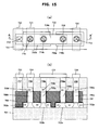
- FIG. 15(a) is a top plan view showing a composite NMOS SGT having a gate length of 4Ls, according to a fifth embodiment of the present invention
- FIG. 15(b) is a sectional view taken along the cutting-plane line A-A' in FIG. 15(a) .
- the composite NMOS SGT having a gate length of 4Ls will be described below.
- a first planar silicon layer 702a and a second planar silicon layer 702b are formed on a buried oxide film layer 701.
- Two pillar-shaped silicon layers 705a, 705b are formed on the first planar silicon layer 702a, and two pillar-shaped silicon layers 705c, 705d are formed on the second planar silicon layer 702b.
- An N + lower diffusion layer 703a is formed in the first planar silicon layer 702a, and an N + lower diffusion layer 703b is formed in the second planar silicon layer 702b.
- a gate dielectric film 707 and a gate electrode 708 are formed around the pillar-shaped silicon layers 705a, 705b, 705c, 705d.
- the pillar-shaped silicon layers 705a, 705b, 705c, 705d are connected in series through the lower diffusion layer 703a, an interconnection layer 723 and the lower diffusion layer 703b.
- the gate electrode 708 is connected to an interconnection layer 722 via a contact 717.
- An interconnection layer 720 serving as a source electrode is connected to an upper diffusion layer 709a of the pillar-shaped silicon layer 705a via a contact 715, and an interconnection layer 721 serving as a drain electrode is connected to an upper diffusion layer 709d of the pillar-shaped silicon layer 705d via a contact 716.
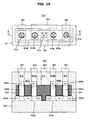
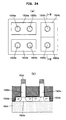
- FIGS. 16(a) and 16(b) show an example of modification of the composite NMOS SGT having a gate length of 4Ls.
- a contact 817 is formed on the gate electrode at a position corresponding to an element isolation region between the first and second planar silicon layers. This makes it possible to reduce a transistor occupancy area as compared with the composite NMOS SGT in FIGS. 15(a) and 15(b) .
- the remaining structure is the same as that in FIG. 15 .
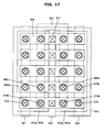
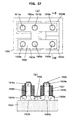
- FIG. 17 is a top plan view showing a composite NMOS SGT which is formed by connecting in parallel a plurality of sets of series-connected four unit SGTs, to have a gate length of 4Ls, according to a sixth embodiment of the present invention.
- a plurality of the composite SGTs each fabricated as shown in FIGS. 16(a) and 16(b) to have a gate length of 4Ls are connected in parallel so as to form a transistor having a large drive current.
- a first planar silicon layer 902a and a second planar silicon layer 902b are formed on a buried oxide film layer 901 along a row direction.
- a plurality of (e.g., five) pillar-shaped silicon layers 905a and a plurality of (e.g., five) pillar-shaped silicon layers 905b are formed on the first planar silicon layer 902a in parallel with each other with respect to a column direction.
- a plurality of (e.g., five) pillar-shaped silicon layers 905c and a plurality of (e.g., five) pillar-shaped silicon layers 905d are formed on the second planar silicon layer 902b in parallel with each other with respect to the column direction.
- An N + lower diffusion layer 903a is formed in the first planar silicon layer 902a, and an N + lower diffusion layer 903b is formed in the second planar silicon layer 902b.
- a gate electrode 908 is commonly formed around each of a plurality of (e.g., five) sets of the four pillar-shaped silicon layers 905a, 905b, 905c, 905d aligned in the row direction, through a gate dielectric film.
- Each of the sets of four pillar-shaped silicon layers 905a, 905b, 905c, 905d are connected in series through the lower diffusion layer 903a, an interconnection layer 923 and the lower diffusion layer 903b.
- Each of the gate electrodes 908 is connected to an interconnection layer 922 via a contact 917 formed thereon.
- An interconnection layer 920 serving as a source electrode is connected to an upper diffusion layer of the pillar-shaped silicon layer 905a via a contact 915, and an interconnection layer 921 serving as a drain electrode is connected to an upper diffusion layer of the pillar-shaped silicon layer 905d via a contact 916.
- FIG. 18 is a top plan view showing an example of modification of the composite NMOS SGT which is formed by connecting in parallel a plurality of sets of series-connected four unit SGTs, to have a gate length of 3Ls.
- a layout in FIG. 18 is different from that in FIG. 17 , in terms of a technique of gate interconnection.
- the number of contacts to be formed on the gate electrodes is increased by just an increase in the number of unit SGTs to be connected in parallel.
- the layout illustrated in FIG. 18 even if the number of the sets of series-connected four unit SGTs to be connected in parallel is increased, the number of contacts to be formed on the gate electrodes is never increased, so that a transistor occupancy area is reduced accordingly.
- a first planar silicon layer 1002a and a second planar silicon layer 10002b are formed on a buried oxide film layer 1001 along a row direction.
- a plurality of (e.g., five) pillar-shaped silicon layers 1005a and a plurality of (e.g., five) pillar-shaped silicon layers 1005b are formed on the first planar silicon layer 1002a in parallel with each other with respect to a column direction.
- a plurality of (e.g., five) pillar-shaped silicon layers 1005c and a plurality of (e.g., five) pillar-shaped silicon layers 1005d are formed on the second planar silicon layer 1002b in parallel with each other with respect to the column direction.
- An N + lower diffusion layer 1003a is formed in the first planar silicon layer 1002a, and an N + lower diffusion layer 1003b is formed in the second planar silicon layer 1002b.
- a gate electrode 1008a is commonly formed around the plurality of pillar-shaped silicon layers 1005a through a gate dielectric film, and a gate electrode 1008b is commonly formed around the plurality of pillar-shaped silicon layers 1005b through a gate dielectric film.
- a gate electrode 1008c is commonly formed around the plurality of pillar-shaped silicon layers 1005c through a gate dielectric film
- a gate electrode 1008d is commonly formed around the plurality of pillar-shaped silicon layers 1005d through a gate dielectric film.
- Each of a plurality of (e.g., five) sets of the four pillar-shaped silicon layers 1005a, 1005b, 1005c, 1005d aligned in the row direction are connected in series through the lower diffusion layer 1003a, an interconnection layer 1023 and the lower diffusion layer 1003b.
- Each of the gate electrodes 1008a, 1008b, 1008c, 1008d is connected to an interconnection layer 1022 via a contact 1017 formed thereon, and an interconnection layer 1020 serving as a source electrode is connected to an upper diffusion layer of the pillar-shaped silicon layer 1005a via a contact 1015, and an interconnection layer 1021 serving as a drain electrode is connected to an upper diffusion layer of the pillar-shaped silicon layer 1005d via a contact 1016.
- the contact 1017 for each of the gate electrodes is formed at each of opposite ends of a respective one of the four columns of unit SGTs to be connected in parallel.
- the contact may be formed on only one of the ends.
- FIG. 19 is an equivalent circuit diagram of a CMOS inverter according to a seventh embodiment of the present invention. A circuit operation of the CMOS inverter will be described below.
- An input signal Vin 1 is applied to a gate of an NMOS Qn 1 and a gate of a PMOS Qp 1. When the Vin 1 is "1", the NMOS Qn 1 is placed in an ON state, and the PMOS Qp 1 is placed in an OFF state, so that an output signal Vout 1 becomes "0".
- each of the NMOS (Qn 1) and the PMOS (Qp 1) has a structure where two unit SGTs are connected in series.
- FIG. 20 is a top plan view showing the CMOS inverter according to the seventh embodiment
- FIGS. 21(a) and 21(b) are sectional views taken along the cutting-plane line A-A' and the cutting-plane line B-B' in FIG. 20 , respectively.
- the CMOS inverter will be described below.
- Two planar silicon layers 1101, 1102 are formed on a buried oxide layer 1100.
- Two pillar-shaped silicon layers 1105a, 1105b are formed on the planar silicon layer 1101, and two pillar-shaped silicon layers 1106a, 1106b are formed on the planar silicon layer 1102.
- a gate dielectric film 1107 and a gate electrode 1108a are formed to surround the pillar-shaped silicon layers 1105a, 1106a, and a gate dielectric film 1107 and a gate electrode 1108b are formed to surround the pillar-shaped silicon layers 1105b, 1106b.
- An N + lower diffusion layer 1103 is formed in the planar silicon layer 1101 underneath the pillar-shaped silicon layers 1105a, 1105b each constituting a unit NMOS SGT.
- An N + upper diffusion layer 1109a is formed in an upper portion of the pillar-shaped silicon layer 1105a, and an N + upper diffusion layer 1109b is formed in an upper portion of the pillar-shaped silicon layer 1105b.
- a P + lower diffusion layer 1104 is formed in the planar silicon layer 1102 underneath the pillar-shaped silicon layers 1106a, 1106b each constituting a unit PMOS SGT.
- a P + upper diffusion layer 1110a is formed in an upper portion of the pillar-shaped silicon layer 1106a
- a P + upper diffusion layer 1110b is formed in an upper portion of the pillar-shaped silicon layer 1106b.
- a composite NMOS SGT is formed by connecting in series the two unit SGTs comprising the two pillar-shaped silicon layers 1105a, 1105b
- a composite PMOS SGT is formed by connecting in series the two unit SGTs comprising the two pillar-shaped silicon layers 1106a, 1106b.
- a contact 1115 formed on the upper diffusion layer 1109 of the pillar-shaped silicon layer 1105a is connected to a ground potential through an interconnection layer 1120, and a contact 1116 formed on the upper diffusion layer 1110a of the pillar-shaped silicon layer 1106a is connected to a power supply potential through an interconnection layer 1121.
- the gate electrodes 1108a, 1108b are connected to an input terminal (interconnection line 1122), via respective contacts 1117a, 1117b formed thereon, and two contacts 1118a, 1118b formed on respective ones of the upper diffusion layers 1109b, 1110b of the pillar-shaped silicon layers 1105b, 1116b are connected to an output terminal through an interconnection layer 1123. In this manner, the CMOS inverter is formed.
- each of the composite NMOS SGT and the composite PMOS SGT has a structure where two unit SGTs are connected in series.
- the CMOS inverter is fabricated using the composite NMOS SGT and the composite PMOS SGT each having a substantial gate length of 2Ls.
- FIG. 22 is a top plan view showing a CMOS inverter which comprises a composite NMOS SGT and a composite PMOS SGT each formed by connecting in parallel a plurality of (e.g., five) sets of series-connected two unit SGTs, to have a gate length of 2Ls.
- the number of sets of the series-connected two unit SGTs in each of the composite NMOS SGT and the composite PMOS SGT can be appropriately determined to adjust performance of the CMOS inverter.
- Two planar silicon layers 1201, 1202 are formed on a buried oxide layer 1200 along a column direction.
- a plurality of (e.g., five) pillar-shaped silicon layers 1205a and a plurality of (e.g., five) pillar-shaped silicon layers 1205b are formed on the planar silicon layer 1201 in parallel with each other with respect to the column direction.
- a plurality of (e.g., five) pillar-shaped silicon layers 1206a and a plurality of (e.g., five) pillar-shaped silicon layers 1206b are formed on the planar silicon layer 1202 in parallel with each other with respect to the column direction.
- a gate dielectric film and a gate electrode 1208a are formed to surround a group of the pillar-shaped silicon layers 1205a, 1206a aligned in the column direction, and a gate dielectric film and a gate electrode 1208b are formed to surround the a group of the pillar-shaped silicon layers 1205b, 1206b aligned in the column direction.
- An N + lower diffusion layer 1203 is formed in the planar silicon layers 1201 underneath the pillar-shaped silicon layers 1205a, 1205b each constituting a unit NMOS SGT, and an N + upper diffusion layer is formed in an upper portion of each of the pillar-shaped silicon layers 1205a, 1205b.
- a P + lower diffusion layer 1204 is formed in the planar silicon layers 1202 underneath the pillar-shaped silicon layers 1206a, 1206b each constituting a unit PMOS SGT, and a P + upper diffusion layer is formed in an upper portion of each of the pillar-shaped silicon layers 1206a, 1206b.
- a composite NMOS SGT is formed by connecting in series the two unit SGTs comprising the two pillar-shaped silicon layers 1205a, 1205b in each of a plurality of (e.g., five) rows
- a composite PMOS SGT is formed by connecting in series the two unit SGTs comprising the two pillar-shaped silicon layers 1206a, 1206b in each of the plurality of rows.
- a contact 1215 formed on each of the upper diffusion layers of the pillar-shaped silicon layers 1205a is connected to a ground potential through an interconnection layer 1220, and a contact 1216 formed on each of the upper diffusion layers of the pillar-shaped silicon layers 1206a is connected to a power supply potential through an interconnection layer 1221.
- a contact 1217a formed on the gate electrode 1208a, and a contact 1217b formed on the gate electrode 1208b, are connected to an input terminal (interconnection layer 1222).
- a contact 1218a formed on each of the upper diffusion layers of the pillar-shaped silicon layers 1205b, and a contact 1218b formed on each of the upper diffusion layers of the pillar-shaped silicon layers 1216b are connected to an output terminal through an interconnection layer 1223. In this manner, the CMOS inverter is formed.
- one of the two gate electrodes is shared by the plurality of unit NMOS SGTs and the plurality of unit PMOS SGTs in a first column, and the other gate electrode is shared by the plurality of unit NMOS SGTs and the plurality of unit PMOS SGTs in a second column.
- this gate electrode layout even if the number of the sets of series-connected two unit SGTs to be connected in parallel is increased, it is not required to increase the number of contacts to be formed on the gate electrodes. This makes it possible to form a CMOS inverter having a small occupancy area.
- a plurality of contacts may be additionally formed at the end of the gate electrode to reduce a delay in voltage to the gate electrode.
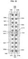
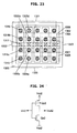
- FIG. 23 is a top plan view showing an example of modification of the CMOS inverter which comprises a composite NMOS SGT and a composite PMOS SGT each formed by connecting in parallel a plurality of sets of series-connected two unit SGTs, to have a gate length of 2Ls.
- one gate electrode is shared by two unit NMOS SGTs (i.e., one composite NMOS SGT) and two unit PMOS SGTs (i.e., one composite PMOS SGT) in each of a plurality of columns.
- Two planar silicon layers 1301, 1302 are formed on a buried oxide layer 1300 along a column direction.
- a plurality of (e.g., five) pillar-shaped silicon layers 1305a and a plurality of (e.g., five) pillar-shaped silicon layers 1305b are formed on the planar silicon layer 1301 in parallel with each other with respect to a row direction.
- a plurality of (e.g., five) pillar-shaped silicon layers 1305c and a plurality of (e.g., five) pillar-shaped silicon layers 1305d are formed on the planar silicon layer 1302 in parallel with each other with respect to the row direction.
- a gate electrode 1308 is commonly formed around a group of the four pillar-shaped silicon layers 1305a, 1305b, 1305c, 1305d in each of a plurality of (e.g., five) columns.
- An N + lower diffusion layer 1303 is formed in the planar silicon layers 1301 underneath the pillar-shaped silicon layers 1305a, 1305b each constituting a unit NMOS SGT, and an N + upper diffusion layer is formed in an upper portion of each of the pillar-shaped silicon layers 1305a, 1305b.
- a P + lower diffusion layer 1304 is formed in the planar silicon layers 1302 underneath the pillar-shaped silicon layers 1305c, 1305d each constituting a unit PMOS SGT, and a P + upper diffusion layer is formed in an upper portion of each of the pillar-shaped silicon layers 1305c, 1305d.
- a composite NMOS SGT is formed by arranging in parallel the plurality of sets of series-connected two unit SGTs comprising the two pillar-shaped silicon layers 1305a, 1305b
- a composite PMOS SGT is formed by arranging in parallel the plurality of series-connected unit SGTs comprising the two pillar-shaped silicon layers 1305c, 1305d.
- a contact 1315 formed on each of the upper diffusion layers of the pillar-shaped silicon layers 1305a is connected to a ground potential through an interconnection layer 1320, and a contact 1316 formed on each of the upper diffusion layers of the pillar-shaped silicon layers 1305d is connected to a power supply potential through an interconnection layer 1321.
- a contact 1317 formed on each of the gate electrodes 1308 is connected to an input terminal (interconnection layer 1322).
- a contact 1318a formed on each of the upper diffusion layers of the pillar-shaped silicon layers 1305b, and a contact 1318b formed on each of the upper diffusion layers of the pillar-shaped silicon layers 1305c, are connected to an output terminal through an interconnection layer 1323. In this manner, the CMOS inverter is formed.
- FIG. 24 is an equivalent circuit diagram of a CMOS inverter according to a ninth embodiment of the present invention. A circuit operation of the CMOS inverter will be described below.
- An input signal Vin 2 is applied to a gate of an NMOS Qn 2 and a gate of a PMOS Qp 2. When the Vin 2 is "1", the NMOS Qn 2 is placed in an ON state, and the PMOS Qp 2 is placed in an OFF state, so that an output signal Vout 2 becomes "0".
- each of the NMOS (Qn 2) and the PMOS (Qp 2) has a structure where three unit SGTs are connected in series.
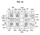
- FIG. 25 is a top plan view showing a CMOS inverter according to the ninth embodiment.
- FIGS. 26(a) and 26(b) are sectional views taken along the cutting-plane line A-A' and the cutting-plane line B-B' in FIG. 25 , respectively.
- the CMOS inverter according to the ninth embodiment will be described below.
- planar silicon layers 1401a, 1401b, 1402a, 1402b are formed on a buried oxide film layer 1400 in a two-row by two-column arrangement.
- Two pillar-shaped silicon layers 1405a, 1405b are formed on the planar silicon layer 1401a, and a pillar-shaped silicon layer 1405c is formed on the planar silicon layer 1401b.
- Two pillar-shaped silicon layers 1406a, 1406b are formed on the planar silicon layer 1402a, and a pillar-shaped silicon layer 1406c is formed on the planar silicon layer 1402b.
- a gate dielectric film and a gate electrode 1408 are formed around each of three sets of the two pillar-shaped silicon layers aligned in a column direction.
- An N + lower diffusion layer 1403a is formed in the planar silicon layer 1401a underneath the pillar-shaped silicon layers 1405a, 1405b each constituting a unit NMOS SGT.
- An N + upper diffusion layer 1409a is formed in an upper portion of the pillar-shaped silicon layer 1405a, and an N + upper diffusion layer 1409b is formed in an upper portion of the pillar-shaped silicon layer 1405b.
- An N + lower diffusion layer 1403b is formed in the planar silicon layer 1401b underneath the pillar-shaped silicon layer 1405c constituting a unit NMOS SGT, and an N + upper diffusion layer 1409c is formed in an upper portion of the pillar-shaped silicon layer 1405c.
- a P + lower diffusion layer 1404a is formed in the planar silicon layer 1402a underneath the pillar-shaped silicon layers 1406a, 1406b each constituting a unit PMOS SGT.
- a P + upper diffusion layer 1410a is formed in an upper portion of the pillar-shaped silicon layer 1406a, and a P + upper diffusion layer 1410b is formed in an upper portion of the pillar-shaped silicon layer 1406b.
- a P + lower diffusion layer 1404b is formed in the planar silicon layer 1402b underneath the pillar-shaped silicon layer 1406c constituting a unit PMOS SGT, and a P + upper diffusion layer 1410c is formed in an upper portion of the pillar-shaped silicon layer 1406c.
- a composite NMOS SGT is formed by connecting in series the three unit SGTs comprising the pillar-shaped silicon layers 1405a, 1405b, 1405c aligned in a row direction
- a composite PMOS SGT is formed by connecting in series the three unit SGTs comprising the pillar-shaped silicon layers 1406a, 1406b, 1406c aligned in the row direction.
- a contact 1415 formed on the upper diffusion layer 1409a of the pillar-shaped silicon layer 1405a is connected to a ground potential through an interconnection layer 1420, and a contact 1416 formed on the upper diffusion layer 1410a of the pillar-shaped silicon layer 1406a is connected to a power supply potential through an interconnection layer 1421.
- the three gate electrodes 1408a, 148b, 148c are connected to an input terminal (interconnection line 1422), via respective contacts 1417a, 1417b, 1417c formed thereon, and two contacts 1418c, 1419c formed on respective ones of the planar silicon layers 1403b, 1404b are connected to an output terminal through an interconnection layer 1423. In this manner, the CMOS inverter is formed.
- each of the composite NMOS SGT and the composite PMOS SGT has a structure where three unit SGTs are connected in series.
- the CMOS inverter is fabricated using the composite NMOS SGT and the composite PMOS SGT each substantially having a gate length of 3Ls.
- a tenth embodiment of the present invention shows another example of the CMOS inverter fabricated using a composite SGT having a gate length three times greater than a gate length Ls of a unit SGT (i.e., having a gate length of 3Ls).
- the tenth embodiment can reduce an occupancy area of a CMOS inverter.
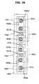
- FIG. 27 is a top plan view showing a CMOS inverter according to the tenth embodiment.
- FIGS. 28(a) and 28(b) are sectional views taken along the cutting-plane line A-A' and the cutting-plane line B-B' in FIG. 27 , respectively.
- an N + lower diffusion layer 1503b and a P + lower diffusion layer 1504b which correspond to the lower diffusion layers 1403b, 1404b separated from each other in the ninth embodiment, are connected to each other by a silicide layer 1532 formed thereon, and a contact 1518c to be connected to an output terminal is formed on a junction region between the N + lower diffusion layer and the P + lower diffusion layer.
- a silicide layer 1532 formed thereon
- a contact 1518c to be connected to an output terminal is formed on a junction region between the N + lower diffusion layer and the P + lower diffusion layer.
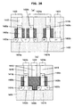
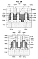
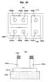
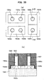
- FIGS. 29(a) to 38(b) one example of a production method for such a CMOS inverter will be described.
- the figure suffixed with (a) is a top plan view
- the figure suffixed with (b) is a sectional view taken along the cutting-plane line B-B' in the figure suffixed with (a).
- a silicon nitride film 1530 serving as a hard mask is formed on a silicon layer on a buried oxide film layer 1500, and the hard mask 1530 and the silicon layer are etched to form six pillar-shaped silicon layers 1505a, 1505b, 1505c, 1506a, 1506b, 1506c. The etching is performed to form a continuous planar silicon layer 1502 underneath the pillar-shaped silicon layers.
- the continuous planar silicon layer 1502 is etched to form an element isolation region therein so as to form three planar silicon layers 1502a, 1502b, 1502c.
- an impurity such as phosphorus (P) or arsenic (As)
- P phosphorus
- As arsenic
- an impurity such as boron (B) or boron difluoride (BF 2 )
- B boron
- BF 2 boron difluoride
- the silicon nitride film 1530 on a top of each of the pillar-shaped silicon layers functions as a stopper for preventing the impurity from being implanted into an upper portion of the pillar-shaped silicon layer.
- a gate dielectric film 1507 and a gate conductive film 1508 are formed.
- a thickness of the gate dielectric film may be increased as compared with cases where it is used in a logic circuit section.
- the gate conductive film 1508 and the gate dielectric film 1507 located above the pillar-shaped silicon layers are polished by chemical mechanical polishing (CMP), to flatten a top surface of the gate conductive film.
- CMP chemical mechanical polishing
- the flattening of the top surface of the gate conductive film by CMP makes it possible to improve a configuration of the gate conductive film to facilitate control of a gate length.
- the silicon nitride film 1530 on the top of each of the pillar-shaped silicon layers is used as a CMP stopper.
- the use of the silicon nitride film 1530 as a CMP stopper makes it possible to control an amount of CMP with high repeatability.
- the gate conductive film 1508 is etched back in such a manner that the gate conductive film 1508 is formed to have a desired gate length, i.e., a gate length is set.
- the silicon nitride film 1530 as a hard mask is removed by etching, and then a gate electrode 1508 is formed by lithography and dry etching.
- an impurity such P or As
- an impurity is introduced into an upper portion of each of the pillar-shaped silicon layers 1505a, 1505b, 1505c by impurity implantation or the like, to form an N + source/drain diffusion layer (1509a, 1509b, 1509c) therein
- an impurity, such B or BF 2 is introduced into an upper portion of each of the pillar-shaped silicon layers 1506a, 1506b, 1506c by impurity implantation or the like, to form a P + source/drain diffusion layer (1510a, 1510b, 1510c) therein
- a silicon nitride film is formed, and etched back to form a nitride film-based sidewall 1531.
- a silicide layer is formed on respective surfaces of the planar silicon layers 1501b, 1502b, and respective top surfaces of the pillar-shaped silicon layers.
- an interlayer dielectric film is formed, eight contacts 1513, 1514, 1515, 1516, 1517, 1518a, 1518b, 1518c, 1519a, 1519b are formed. Then, six interconnection layers 1520, 1521, 1522, 1523, 1524a, 1524b are formed.
- each of the composite NMOS SGT and the composite PMOS SGT has a structure where three unit SGTs are connected in series.
- the CMOS inverter is fabricated using the composite NMOS and the composite PMOS each substantially having a gate length of 3 Ls.
- the lower diffusion layers 1503b, 1504b are connected to each other by the silicide layer 1532. This makes it possible to reduce an inverter occupancy area.
- FIG. 39 shows a CMOS inverter according to an eleventh embodiment of the present invention, as yet another example of the CMOS inverter fabricated using a composite SGT having a gate length three times greater than a gate length Ls of a unit SGT (i.e., having a gate length of 3Ls).
- a layout of three planar silicon layers is changed from that in the tenth embodiment, in such a manner as to allow two gate electrodes to be arranged in a linear pattern. This makes it possible to facilitate patterning of the gate electrodes as compared with the tenth embodiment.
- two lower diffusion layers 1603b, 1604b are connected to each other by a silicide layer formed on respective surfaces thereof to allow an occupancy area of a CMOS inverter to be reduced.
- the remaining structure is the same as that in the tenth embodiment.
- FIG. 40 is a top plan view showing a CMOS inverter which comprises a composite NMOS SGT and a composite PMOS SGT each formed by connecting in parallel a plurality of sets of series-connected three unit SGTs, to have a gate length of 3Ls, according to a twelfth embodiment of the present invention.
- the sets of series-connected three unit SGTs in each of the composite NMOS SGT and the composite PMOS SGT can be connected in parallel in an appropriate number to adjust performance of the CMOS inverter.
- a gate electrode 1708a is shared by a plurality of (e.g., five) unit NMOS SGTs each comprising a pillar-shaped silicon layer 1705a arranged in a first column, and a plurality of (e.g., five) unit PMOS SGTs each comprising a pillar-shaped silicon layer 1706a arranged in the first column.
- NMOS SGTs each comprising a pillar-shaped silicon layer 1705a arranged in a first column
- PMOS SGTs each comprising a pillar-shaped silicon layer 1706a arranged in the first column.
- a gate electrode 1708b is shared by a plurality of (e.g., five) unit NMOS SGTs each comprising a pillar-shaped silicon layer 1705b arranged in a second column, a plurality of (e.g., five) unit NMOS SGTs each comprising a pillar-shaped silicon layer 1705c arranged in a third column, a plurality of (e.g., five) unit PMOS SGTs each comprising a pillar-shaped silicon layer 1706b arranged in the second column, and a plurality of (e.g., five) unit PMOS SGTs each comprising a pillar-shaped silicon layer 1706c arranged in the third column.
- FIG. 41 is a top plan view showing an example of modification of the CMOS inverter which comprises a composite NMOS SGT and a composite PMOS SGT each formed by connecting in parallel a plurality of sets of series-connected three unit SGTs, to have a gate length of 3Ls.
- the CMOS inverter illustrated in FIG. 41 illustrates an example of modification of the CMOS inverter which comprises a composite NMOS SGT and a composite PMOS SGT each formed by connecting in parallel a plurality of sets of series-connected three unit SGTs, to have a gate length of 3Ls.
- an NMOS gate electrode 1808a in each of a plurality of columns is shared by a unit NMOS SGT comprising a pillar-shaped silicon layer 1805a arranged in a first row, a unit NMOS SGT comprising a pillar-shaped silicon layer 1805b arranged in a second row, and a unit NMOS SGT comprising a pillar-shaped silicon layer 1805c arranged in a third row.
- a PMOS gate electrode 1808b in each of the plurality of columns is shared by a unit PMOS SGT comprising a pillar-shaped silicon layer 1806a arranged in a fourth row, a unit PMOS SGT comprising a pillar-shaped silicon layer 1806b arranged in a fifth row, and a unit PMOS SGT comprising a pillar-shaped silicon layer 1806c arranged in a sixth row.
- this gate electrode layout even if the number of the sets of series-connected three unit SGTs to be connected in parallel is increased, the number of unit SGTs to be connected to one gate electrode can be kept constant. This makes it possible to significantly reduce a delay in gate voltage.
- FIG. 42 is an equivalent circuit diagram of a CMOS inverter according to a thirteenth embodiment of the present invention. A circuit operation of the CMOS inverter will be described below.
- An input signal Vin 3 is applied to a gate of an NMOS Qn 3 and a gate of a PMOS Qp 3. When the Vin 3 is "1", the NMOS Qn 3 is placed in an ON state, and the PMOS Qp 3 is placed in an OFF state, so that an output signal Vout 3 becomes "0".
- each of the NMOS (Qn 3) and the PMOS (Qp 3) has a structure where four unit SGTs are connected in series.
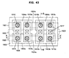
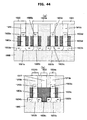
- FIG. 43 is a top plan view showing a CMOS inverter according to the thirteenth embodiment.
- FIGS. 44(a) and 44(b) are sectional views taken along the cutting-plane line A-A' and the cutting-plane line B-B' in FIG. 43 , respectively.
- the CMOS inverter according to the thirteenth embodiment will be described below.
- planar silicon layers 1901a, 1901b, 1902a, 1902b are formed on a buried oxide film layer 1900 in a two-row by two-column arrangement.
- Two pillar-shaped silicon layers 1905a, 1905b are formed on the planar silicon layer 1901a, and two pillar-shaped silicon layers 1905c, 1905d are formed on the planar silicon layer 1901b.
- Two pillar-shaped silicon layers 1906a, 1906b are formed on the planar silicon layer 1902a, and two pillar-shaped silicon layers 1906c, 1906d are formed on the planar silicon layer 1902b.
- a gate dielectric film and a gate electrode 1908a are formed around the pillar-shaped silicon layers 1905a, 1906a, and a gate dielectric film and a gate electrode 1908b are formed around the pillar-shaped silicon layers 1905b, 1906b.
- a gate dielectric film and a gate electrode 1908c are formed around the pillar-shaped silicon layers 1905c, 1906c, and a gate dielectric film and a gate electrode 1908d are formed around the pillar-shaped silicon layers 1905d, 1906d.
- An N + lower diffusion layer 1903a is formed in the planar silicon layer 1901a underneath the pillar-shaped silicon layers 1905a, 1905b each constituting a unit NMOS SGT.
- An N + upper diffusion layer 1909a is formed in an upper portion of the pillar-shaped silicon layer 1905a, and an N + upper diffusion layer 1909b is formed in an upper portion of the pillar-shaped silicon layer 1905b.
- An N + lower diffusion layer 1903b is formed in the planar silicon layer 1901b underneath the pillar-shaped silicon layers 1905c, 1905d each constituting a unit NMOS SGT.
- An N + upper diffusion layer 1909c is formed in an upper portion of the pillar-shaped silicon layer 1905c, and an N + upper diffusion layer 1909d is formed in an upper portion of the pillar-shaped silicon layer 1905d.
- a P + lower diffusion layer 1904a is formed in the planar silicon layer 1902a underneath the pillar-shaped silicon layers 1906a, 1906b each constituting a unit PMOS SGT.
- a P + upper diffusion layer 1910a is formed in an upper portion of the pillar-shaped silicon layer 1906a, and a P + upper diffusion layer 1910b is formed in an upper portion of the pillar-shaped silicon layer 1906b.
- a P + lower diffusion layer 1904b is formed in the planar silicon layer 1902b underneath the pillar-shaped silicon layers 1906c, 1906d each constituting a unit PMOS SGT.
- a P + upper diffusion layer 1910c is formed in an upper portion of the pillar-shaped silicon layer 1906c, and a P + upper diffusion layer 1910d is formed in an upper portion of the pillar-shaped silicon layer 1906d.
- a composite NMOS SGT is formed by connecting in series the four unit SGTs comprising the four pillar-shaped silicon layers 1905a, 1905b, 1905c, 1905d aligned in a row direction
- a composite PMOS SGT is formed by connecting in series the four unit SGTs comprising the four pillar-shaped silicon layers 1906a, 1906b, 1906c, 1906d aligned in the row direction.
- a contact 1915 formed on the upper diffusion layer 1909a of the pillar-shaped silicon layer 1905a is connected to a ground potential through an interconnection layer 1920, and a contact 1916 formed on the upper diffusion layer 1910a of the pillar-shaped silicon layer 1906a is connected to a power supply potential through an interconnection layer 1921.
- the four gate electrodes 1908a, 1908b, 1908c, 1908d are connected to an interconnection line 1922 serving as an input terminal, via respective contacts 1917 formed thereon, and two contacts 1918c, 1919c formed on respective ones of the upper diffusion layers 1909d, 1910d of the pillar-shaped silicon layers 1905d, 1906d are connected to an output terminal through an interconnection layer 1923. In this manner, the CMOS inverter is formed.
- each of the composite NMOS SGT and the composite PMOS SGT has a structure where four unit SGTs are connected in series.
- the CMOS inverter is fabricated using the composite NMOS SGT and the composite PMOS SGT each substantially having a gate length of 4Ls.
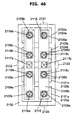
- FIG. 45 is a top plan view showing an example of modification of the CMOS inverter which comprises a composite NMOS SGT and a composite PMOS SGT each formed by connecting in parallel a plurality of sets of series-connected four unit SGTs, to have a gate length of 4Ls.
- the modified CMOS inverter will be specifically described below.
- Four planar silicon layers 2001a, 2001b, 2002a, 2002b are formed on a buried oxide layer 2000 in a two-row by two-column arrangement.
- a plurality of (e.g., five) pillar-shaped silicon layers 2005a and a plurality of (e.g., five) pillar-shaped silicon layers 2005b are formed on the planar silicon layer 2001a in parallel with each other with respect to a column direction, and a plurality of (e.g., five) pillar-shaped silicon layers 2005c and a plurality of (e.g., five) pillar-shaped silicon layers 2005d are formed on the planar silicon layer 2001b in parallel with each other with respect to the column direction.
- a plurality of (e.g., five) pillar-shaped silicon layers 2006a and a plurality of (e.g., five) pillar-shaped silicon layers 2006b are formed on the planar silicon layer 2002a in parallel with each other with respect to the column direction, and a plurality of (e.g., five) pillar-shaped silicon layers 2006c and a plurality of (e.g., five) pillar-shaped silicon layers 2006d are formed on the planar silicon layer 2002b in parallel with each other with respect to the column direction.
- a gate dielectric film and a gate electrode 2008a is formed to surround a group of the pillar-shaped silicon layers 2005a, 2006a aligned in the column direction, and a gate dielectric film and a gate electrode 2008b is formed to surround a group of the pillar-shaped silicon layers 2005b, 2006b aligned in the column direction.
- a gate dielectric film and a gate electrode 2008c is formed to surround a group of the pillar-shaped silicon layers 2005c, 2006c aligned in the column direction, and a gate dielectric film and a gate electrode 2008d are formed to surround a group of the pillar-shaped silicon layers 2005d, 2006d aligned in the column direction.
- An N + lower diffusion layer 2003a is formed in the planar silicon layers 2001a underneath the pillar-shaped silicon layers 2005a, 2005b each constituting a unit NMOS SGT, and an N + upper diffusion layer is formed in an upper portion of each of the pillar-shaped silicon layers 2005a, 2005b.
- An N + lower diffusion layer 2003b is formed in the planar silicon layers 2001b underneath the pillar-shaped silicon layers 2005c, 2005d each constituting a unit NMOS SGT, and an N + upper diffusion layer is formed in an upper portion of each of the pillar-shaped silicon layers 2005c, 2005d.
- a P + lower diffusion layer 2004a is formed in the planar silicon layers 2002a underneath the pillar-shaped silicon layers 2006a, 2006b each constituting a unit PMOS SGT, and a P + upper diffusion layer is formed in an upper portion of each of the pillar-shaped silicon layers 2006a, 2006b.
- a P + lower diffusion layer 2004b is formed in the planar silicon layers 2002b underneath the pillar-shaped silicon layers 2006c, 2006d each constituting a unit PMOS SGT, and a P + upper diffusion layer is formed in an upper portion of each of the pillar-shaped silicon layers 2006c, 2006d.
- a composite NMOS SGT is formed by connecting in series the four unit SGTs comprising the four pillar-shaped silicon layers 2005a, 2005b, 2005c, 2005d in each of a plurality of (e.g., five) rows
- a composite PMOS SGTs is formed by connecting in series the four unit SGTs comprising the four pillar-shaped silicon layers 2006a, 2006b, 2006c, 2006d in each of the plurality of rows.
- a contact 2015 formed on each of the upper diffusion layers of the pillar-shaped silicon layers 2005a is connected to a ground potential through an interconnection layer 2020, and a contact 2016 formed on each of the upper diffusion layers of the pillar-shaped silicon layers 2006a is connected to a power supply potential through an interconnection layer 2021.
- Each of the gate electrodes 2008a, 2008b, 2008c, 2008d is connected to an interconnection layer 2022 serving as an input terminal, via respective contacts 2017 formed thereon.
- a contact 2018c formed on each of the upper diffusion layers of the pillar-shaped silicon layers 2005d, and a contact 2019c formed on each of the upper diffusion layers of the pillar-shaped silicon layers 2006d, are connected to an output terminal (interconnection layer 2023). In this manner, the CMOS inverter is formed.
- the sets of series-connected four unit SGTs in each of the composite NMOS SGT and the composite PMOS SGT can be connected in parallel in an appropriate number of to adjust performance of the CMOS inverter.
- the CMOS inverter illustrated in FIG. 45 even if the number of the sets of series-connected four unit SGTs to be connected in parallel is increased, the number of contacts to be formed on the gate electrodes is never increased. This makes it possible to form a CMOS inverter having a small occupancy area.
- a plurality of contacts may be additionally formed at the end of the gate electrode to reduce a delay in voltage to the gate electrode.
- FIG. 46 shows a CMOS inverter according to a fourteenth embodiment of the present invention, as another example of the CMOS inverter fabricated using a composite SGT having a gate length four times greater than a gate length Ls of a unit SGT (i.e., having a gate length of 4Ls).
- a layout of four planar silicon layers is changed from that in the thirteenth embodiment, to allow gate electrodes for the unit NMOS/PMOS SGTs in a first column to be commonized, and allow gate electrodes for the unit NMOS/PMOS SGTs in a second column to be commonized. This makes it possible to reduce the number of contacts to be formed on a gate electrode.
- CMOS inverter With reference to FIG. 46 , the CMOS inverter according to the fourteenth embodiment will be described below.
- planar silicon layers 2101a, 2101b, 2102a, 2102b are formed on a buried oxide film layer 2100 along a column direction.
- Two pillar-shaped silicon layers 2105a, 2105b are formed on the planar silicon layer 2101a, and two pillar-shaped silicon layers 2105c, 2105d are formed on the planar silicon layer 2101b.
- Two pillar-shaped silicon layers 2106a, 2106b are formed on the planar silicon layer 2102a, and two pillar-shaped silicon layers 2106c, 2106d are formed on the planar silicon layer 2102b.
- a gate dielectric film and a gate electrode 2108a are formed to surround the pillar-shaped silicon layers 2105b, 2105c, 2106c, 2106b aligned in the column direction, and a gate dielectric film and a gate electrode 2108b are formed to surround the pillar-shaped silicon layers 2105a, 2105d, 2106d, 2106a aligned in the column direction.
- An N + lower diffusion layer 2103a is formed in the planar silicon layer 2101a underneath the pillar-shaped silicon layers 2105a, 2105b each constituting a unit NMOS SGT, and an N + upper diffusion layer is formed in an upper portion of each of the pillar-shaped silicon layers 2105a, 2105b.
- An N + lower diffusion layer 2103b is formed in the planar silicon layer 2101b underneath the pillar-shaped silicon layers 2105c, 2105d each constituting a unit NMOS SGT, and an N + upper diffusion layer is formed in an upper portion of each of the pillar-shaped silicon layers 2105c, 2105d.
- a P + lower diffusion layer 2104a is formed in the planar silicon layer 2102a underneath the pillar-shaped silicon layers 2106a, 2106b each constituting a unit PMOS SGT, and a P + upper diffusion layer is formed in an upper portion of each of the pillar-shaped silicon layers 2106a, 2106b.
- a P + lower diffusion layer 2104b is formed in the planar silicon layer 2102b underneath the pillar-shaped silicon layers 2106c, 2106d each constituting a unit PMOS SGT, and a P + upper diffusion layer is formed in an upper portion of each of the pillar-shaped silicon layers 2106c, 2106d.
- a composite NMOS SGT is formed by connecting in series the four unit SGTs comprising the four pillar-shaped silicon layers 2105a, 2105b, 2105c, 2105d
- a composite PMOS SGT is formed by connecting in series four unit SGTs comprising the four pillar-shaped silicon layers 2106a, 2106b, 2106c, 2106d.
- a contact 2115 formed on the upper diffusion layer of the pillar-shaped silicon layer 2105a is connected to a ground potential through an interconnection layer 2120, and a contact 2116 formed on the upper diffusion layer of the pillar-shaped silicon layer 2106a is connected to a power supply potential through an interconnection layer 2121.
- the two gate electrodes 2108a, 2108b are connected to an interconnection line 2122 serving as an input terminal, via respective contacts 2117a, 2117b formed thereon, and two contacts 2118c, 2119c formed on respective ones of the upper diffusion layers of the pillar-shaped silicon layers 2105d, 2106d are connected to an output terminal through an interconnection layer 2123. In this manner, the CMOS inverter is formed.
- FIG. 47 is a top plan view showing an example of modification of the CMOS inverter which comprises a composite NMOS SGT and a composite PMOS SGT each formed by connecting in parallel a plurality of sets of series-connected four unit SGTs, to have a gate length of 4Ls.
- the sets of series-connected four unit SGTs in each of the composite NMOS SGT and the composite PMOS SGT can be connected in parallel in an appropriate number to adjust performance of the CMOS inverter.
- the CMOS inverter illustrated in FIG. 47 even if the number of the sets of series-connected four unit SGTs to be connected in parallel is increased, the number of contacts to be formed on the gate electrodes is never increased.
- CMOS inverter having a small occupancy area.
- a plurality of contacts may be additionally formed at the end of the gate electrode to reduce a delay in voltage to the gate electrode.
- FIG. 48 shows a CMOS inverter according to a fifteenth embodiment of the present invention, as another example of the CMOS inverter fabricated using a composite SGT having a gate length four times greater than a gate length Ls of a unit SGT (i.e., having a gate length of 4Ls).
- a layout of four planar silicon layers is changed from that in the thirteenth embodiment, in such a manner as to allow all gate electrodes for the unit NMOS/PMOS SGTs to be commonized. This makes it possible to reduce the number of contacts to be formed on the gate electrode.
- the remaining structure is the same as that in the thirteenth embodiment.
- CMOS inverter With reference to FIG. 48 , the CMOS inverter according to the fifteenth embodiment will be specifically described below.
- planar silicon layers 2301a, 2301b, 2302a, 2302b are formed on a buried oxide film layer 2300 along a column direction.
- Two pillar-shaped silicon layers 2305a, 2305b are formed on the planar silicon layer 2301a, and two pillar-shaped silicon layers 2305c, 2305d are formed on the planar silicon layer 2301b.
- Two pillar-shaped silicon layers 2306a, 2306b are formed on the planar silicon layer 2302a, and two pillar-shaped silicon layers 2306c, 2306d are formed on the planar silicon layer 2302b.
- a gate dielectric film and a gate electrode 2308 are formed around all the pillar-shaped silicon layers.
- An N + lower diffusion layer 2303a is formed in the planar silicon layer 2301a underneath the pillar-shaped silicon layers 2305a, 2305b each constituting a unit NMOS SGT, and an N + upper diffusion layer is formed in an upper portion of each of the pillar-shaped silicon layers 2305a, 2305b.
- An N + lower diffusion layer 2303b is formed in the planar silicon layer 2301b underneath the pillar-shaped silicon layers 2305c, 2305d each constituting a unit NMOS SGT, and an N + upper diffusion layer is formed in an upper portion of each of the pillar-shaped silicon layers 2305c, 2305d.
- a P + lower diffusion layer 2304a is formed in the planar silicon layer 2302a underneath the pillar-shaped silicon layers 2306a, 2306b each constituting a unit PMOS SGT, and a P + upper diffusion layer is formed in an upper portion of each of the pillar-shaped silicon layers 2306a, 2306b.
- a P + lower diffusion layer 2304b is formed in the planar silicon layer 2302b underneath the pillar-shaped silicon layers 2306c, 2306d each constituting a unit PMOS SGT, and a P + upper diffusion layer is formed in an upper portion of each of the pillar-shaped silicon layers 2306c, 2306d.
- a composite NMOS SGT is formed by connecting in series the four unit SGTs comprising the four pillar-shaped silicon layers 2305a, 2305b, 2305c, 2305d
- a composite PMOS SGT is formed by connecting in series the four unit SGTs comprising the pillar-shaped silicon layers 2306a, 2306b, 2306c, 2306d.
- a contact 2315 formed on the upper diffusion layer of the pillar-shaped silicon layer 2305a is connected to a ground potential through an interconnection layer 2320, and a contact 2316 formed on the upper diffusion layer of the pillar-shaped silicon layer 2306a is connected to a power supply potential through an interconnection layer 2321.
- the gate electrode 2308 is connected to an interconnection line 2322 serving as an input terminal, via a single contact 2317 formed thereon, and two contacts 2318c, 2319c formed on respective ones of the upper diffusion layers of the pillar-shaped silicon layers 2305d, 2306d are connected to an output terminal through an interconnection layer 2323. In this manner, the CMOS inverter is formed.
- FIG. 49 is a top plan view showing an example of modification of the CMOS inverter which comprises a composite NMOS SGT and a composite PMOS SGT each formed by connecting in parallel a plurality of sets of series-connected four unit SGTs, to have a gate length of 4Ls.
- the sets of series-connected four unit SGTs in each of the composite NMOS SGT and the composite PMOS SGT can be connected in parallel in an appropriate number of to adjust performance of the CMOS inverter.
- the CMOS inverter illustrated in FIG. 49 even if the number of sets of series-connected four unit SGTs to be connected in parallel is increased, the number of contacts to be formed on the single gate electrode is never increased.
- a plurality of contacts may be additionally formed at the end of the gate electrode to reduce a delay in voltage to the gate electrode.
- CMOS inverter With reference to FIG. 49 , the modified CMOS inverter will be described below.
- planar silicon layers 2401a, 2401b, 2402a, 2402b are formed on a buried oxide layer 2400 along a column direction.
- a plurality of (e.g., five) pillar-shaped silicon layers 2405a and a plurality of (e.g., five) pillar-shaped silicon layers 2405b are formed on the planar silicon layer 2401a in parallel with each other with respect to a row direction, and a plurality of (e.g., five) pillar-shaped silicon layers 2405c and a plurality of (e.g., five) pillar-shaped silicon layers 2405d are formed on the planar silicon layer 2401b in parallel with each other with respect to the row direction.
- a plurality of (e.g., five) pillar-shaped silicon layers 2406a and a plurality of (e.g., five) pillar-shaped silicon layers 2406b are formed on the planar silicon layer 2402a in parallel with each other with respect to the row direction, and a plurality of (e.g., five) pillar-shaped silicon layers 2406c and a plurality of (e.g., five) pillar-shaped silicon layers 2406d are formed on the planar silicon layer 2402b in parallel with each other with respect to the row direction.
- a gate dielectric film and a gate electrode 2408 are formed to surround the eight pillar-shaped silicon layers 2405a, 2405b, 2405c, 2405d, 2406a, 2406b, 2406c, 2406d in each of a plurality of (e.g., five) columns.
- An N + lower diffusion layer 2403a is formed in the planar silicon layers 2401a underneath the pillar-shaped silicon layers 2405a, 2405b each constituting a unit NMOS SGT, and an N + upper diffusion layer is formed in an upper portion of each of the pillar-shaped silicon layers 2405a, 2405b.
- An N + lower diffusion layer 2403b is formed in the planar silicon layers 2401b underneath the pillar-shaped silicon layers 2405c, 2405d each constituting a unit NMOS SGT, and an N + upper diffusion layer is formed in an upper portion of each of the pillar-shaped silicon layers 2405c, 2405d.
- a P + lower diffusion layer 2404a is formed in the planar silicon layers 2402a underneath the pillar-shaped silicon layers 2406a, 2406b each constituting a unit PMOS SGT, and a P + upper diffusion layer is formed in an upper portion of each of the pillar-shaped silicon layers 2406a, 2406b.
- a P + lower diffusion layer 2404b is formed in the planar silicon layers 2402b underneath the pillar-shaped silicon layers 2406c, 2406d each constituting a unit PMOS SGT, and a P + upper diffusion layer is formed in an upper portion of each of the pillar-shaped silicon layers 2406c, 2406d.
- a composite NMOS SGT is formed by connecting in series the four unit SGTs comprising the four pillar-shaped silicon layers 2405a, 2405b, 2405c, 2405d in each of the plurality of columns
- a composite PMOS SGT is formed by connecting in series four unit SGTs comprising the pillar-shaped silicon layers 2406a, 2406b, 2406c, 2406d in each of the plurality of columns.
- a contact 2415 formed on each of the upper diffusion layers of the pillar-shaped silicon layers 2405a is connected to a ground potential through an interconnection layer 2420, and a contact 2416 formed on each of the upper diffusion layers of the pillar-shaped silicon layers 2406a is connected to a power supply potential through an interconnection layer 2421.
- Each of the gate electrodes 2408 is connected to an interconnection layer 2422 serving as an input terminal, via respective contacts 2417 formed thereon.
- a contact 2418c formed on each of the upper diffusion layers of the pillar-shaped silicon layers 2405d, and a contact 2419c formed on each of the upper diffusion layers of the pillar-shaped silicon layers 2406d, are connected to an output terminal through an interconnection layer 2323. In this manner, the CMOS inverter is formed.
Landscapes
- Metal-Oxide And Bipolar Metal-Oxide Semiconductor Integrated Circuits (AREA)
- Thin Film Transistor (AREA)
- Insulated Gate Type Field-Effect Transistor (AREA)
Abstract
Description
- The present invention relates to a semiconductor device, and more particularly to an SGT (Surrounding Gate Transistor) which is a vertical MOS transistor comprising a pillar-shaped semiconductor layer having a sidewall serving as a channel region, and a gate electrode formed to surround the channel region.
- With a view to achieving higher integration and higher performance of a semiconductor device, an SGT (Surrounding Gate Transistor) has been proposed which is a vertical transistor comprising a pillar-shaped semiconductor layer formed on a surface of a semiconductor substrate, and a gate formed to surround a sidewall of the pillar-shaped semiconductor layer (see, for example, the following Patent Document 1:
JP 2-188966A -
FIG. 50(a) shows a top plan view of a CMOS inverter fabricated using the SGT disclosed in thePatent Document 1, andFIG. 50(b) is a sectional view taken along the cutting-plane line A-A' in the top plan view ofFIG. 50(a) .
Referring toFIGS. 50(a) and 50(b) , an N-well 2502 and a P-well 2503 are formed in an upper region of aSi substrate 2501. A pillar-shaped silicon layer 2505 constituting a PMOS (PMOS pillar-shaped silicon layer 2505) and a pillar-shaped silicon layer 2506 constituting an NMOS (NMOS pillar-shaped silicon layer 2506) are formed on a surface of the Si substrate, specifically, on respective ones of the N-well region and the P-well region, and agate 2508 is formed to surround the pillar-shaped silicon layers. A P+drain diffusion layer 2510 formed underneath the PMOS pillar-shaped silicon layer, and an N+drain diffusion layer 2512 formed underneath the NMOS pillar-shaped silicon layer, are connected to an output terminal Vout. Asource diffusion layer 2509 formed on a top of the PMOS pillar-shaped silicon layer is connected to a power supply potential Vcc, and asource diffusion layer 2511 formed on a top of the NMOS pillar-shaped silicon layer is connected to a ground potential Vss. Thecommon gate 2508 for the PMOS and the NMOS is connected to an input terminal Vin. In this manner, the CMOS inverter is formed. - Patent Document 1:
JP 2-188966A - As a prerequisite to applying an SGT to actual electronic products such as CPU, there is the following problem. In electronic products such as CPU, a logic circuit section requiring a high-speed operation is fabricated using a transistor having a minimum gate size L, whereas an I/O section for interfacing data communication with the outside is fabricated using a transistor having a longer gate length as compared with the transistor for the logic circuit section, because it is generally operated at an operating voltage greater than that for the logic circuit section. For example, given that an operating voltage for the logic circuit section is 1.0 V, the I/O section is operated at an operating voltage of 1.8 V or 2.5 V. Therefore, the transistor for the I/O section has a gate length about two or three times greater than that of the transistor for the logic circuit section.
Further, in a part of analog circuit sections and logic circuit sections for use in various other electronic products, a transistor having a longer gate length as compared with the transistor for a typical logic circuit section is also used.
As above, in actual electronic products, it is essential to concurrently form a plurality of transistors having various different gate lengths, on a chip. However, due to a basic structure of an elemental or unit SGT, it is difficult to form an SGT having a gate length greater than a gate length Ls of the unit SGT. - In view of the above circumstances, it is an object of the present invention to form a transistor having a gate length greater than a gate length Ls of a unit SGT.
- In order to achieve this object, according a first aspect of the present invention, there is provided a semiconductor device which comprises a first MOS transistor and a second MOS transistor each formed on a substrate, wherein each of the first and second MOS transistors is a vertical transistor in which a source diffusion layer, a drain diffusion layer and a pillar-shaped semiconductor layer are hierarchically arranged in a vertical direction with respect to the substrate while arranging the pillar-shaped semiconductor layer between the source diffusion layer and the drain diffusion layer, and a gate electrode is formed along a sidewall of the pillar-shaped semiconductor layer, and wherein: the first and second MOS transistors have a common gate electrode, and a common first planar diffusion layer formed on the substrate; the first MOS transistor has a first pillar-shaped diffusion layer formed on a top of the pillar-shaped semiconductor layer thereof to serve as the source diffusion layer; and the second MOS transistor has a second pillar-shaped diffusion layer formed on a top of the pillar-shaped semiconductor layer thereof to serve as the drain diffusion layer, and wherein the first and second MOS transistors are connected in series to allow a total gate electrode length to become substantially two times greater than a gate electrode length of each of the first and second MOS transistors.
- Preferably, the semiconductor device according the first aspect of the present invention includes a plurality of sets of the series-connected first and second MOS transistors, which are arranged in parallel, wherein the sets of series-connected first and second MOS transistors include a commonized gate electrode, a commonized source electrode and a commonized drain electrode.
- Preferably, in the semiconductor device according the first aspect of the present invention, the vertical transistor for the first MOS transistor includes a plurality of the pillar-shaped semiconductor layers, and the vertical transistor for the second MOS transistor includes a plurality of the pillar-shaped semiconductor layers, wherein the first MOS transistor has a first gate electrode, and the second MOS transistor has a second gate electrode, and wherein the first and second gate electrodes are connected to an interconnection layer via respective different contacts, so that they are interconnected together through the interconnection layer.
- In the above semiconductor device, each of the first and second gate electrodes may be connected to the interconnection layer via a plurality of contacts positioned at opposite ends thereof.
- According to a second aspect of the present invention, there is provided a semiconductor device which comprises a first MOS transistor, a second MOS transistor and a third MOS transistor each formed on a substrate, wherein each of the first to third MOS transistors is a vertical transistor in which a source diffusion layer, a drain diffusion layer and a pillar-shaped semiconductor layer are hierarchically arranged in a vertical direction with respect to the substrate while arranging the pillar-shaped semiconductor layer between the source diffusion layer and the drain diffusion layer, and a gate electrode is formed along a sidewall of the pillar-shaped semiconductor layer, and wherein: the first to third MOS transistors have a common gate electrode; the first and second MOS transistors have a common first planar diffusion layer formed on the substrate; the third MOS transistor has a second planar diffusion layer formed on the substrate to serve as the drain diffusion layer; each of the second and third MOS transistors has a pillar-shaped diffusion layer formed on a top of the pillar-shaped semiconductor layer thereof, wherein the pillar-shaped diffusion layers of the second and third MOS transistors are connected to each other via a contact and an interconnection layer; and the first MOS transistor has a pillar-shaped diffusion layer formed on a top of the pillar-shaped semiconductor layer thereof to serve as the source diffusion layer, and wherein the first to third MOS transistors are connected in series to operate as a composite MOS transistor having a gate electrode length three times greater than that of each of the first to third MOS transistors.
- Preferably, in the semiconductor device according the second aspect of the present invention, the composite MOS transistor is formed by arranging in parallel a plurality of sets of the series-connected first to third MOS transistors having a gate electrode length three times greater than that of each of the first to third MOS transistors, and wherein the composite MOS transistor is configured to have a commonized gate electrode, a commonized source electrode and a commonized drain electrode to enhance a drive current.
- Preferably, in the semiconductor device according the second aspect of the present invention, the vertical transistor for each of the first to third MOS transistors includes a plurality of the pillar-shaped semiconductor layers, and wherein: the first MOS transistor has a first gate electrode; the second MOS transistor has a second gate electrode; and the third MOS transistor has a third gate electrode, and wherein the first to third gate electrodes are connected to an interconnection layer via respective different contacts, so that they are interconnected together through the interconnection layer.
- In the above semiconductor device, each of the first to third gate electrodes may be connected to the interconnection layer via a plurality of contacts positioned at opposite ends thereof.
- According to a third aspect of the present invention, there is provided a semiconductor device which comprises a first MOS transistor, a second MOS transistor, a third MOS transistor and a fourth MOS transistor each formed on a substrate, wherein each of the first to fourth MOS transistors is a vertical transistor in which a source diffusion layer, a drain diffusion layer and a pillar-shaped semiconductor layer are hierarchically arranged in a vertical direction with respect to the substrate while arranging the pillar-shaped semiconductor layer between the source diffusion layer and the drain diffusion layer, and a gate electrode is formed along a sidewall of the pillar-shaped semiconductor layer, and wherein: the first to fourth MOS transistors have a common gate electrode; the first and second MOS transistors have a common first planar diffusion layer formed on the substrate; the third and fourth MOS transistors have a common second planar diffusion layer formed on the substrate; each of the second and third MOS transistors has a pillar-shaped diffusion layer formed on a top of the pillar-shaped semiconductor layer thereof, wherein the pillar-shaped diffusion layers of the second and third MOS transistors are connected to each other via a contact and an interconnection layer; the first MOS transistor has a pillar-shaped diffusion layer formed on a top of the pillar-shaped semiconductor layer thereof to serve as the source diffusion layer; and the fourth MOS transistor has a pillar-shaped diffusion layer formed on a top of the pillar-shaped semiconductor layer thereof to serve as the drain diffusion layer, and wherein the first to fourth MOS transistors are connected in series to operate as a composite MOS transistor having a gate electrode length four times greater than that of each of the first to fourth MOS transistors.
- Preferably, in the semiconductor device according the third aspect of the present invention, the composite MOS transistor is formed by arranging in parallel a plurality of sets of the series-connected first to fourth MOS transistors having a gate electrode length four times greater than that of each of the first to fourth MOS transistors, and wherein the composite MOS transistor is configured to have a commonized gate electrode, a commonized source electrode and a commonized drain electrode to enhance a drive current.
- Preferably, the semiconductor device according the third aspect of the present invention comprises a contact formed on the gate electrode or each of the gate electrodes at a position corresponding to an element isolation region between the first and second planar diffusion layers.
- Preferably, in the semiconductor device according the third aspect of the present invention, the vertical transistor for each of the first to fourth MOS transistors includes a plurality of the pillar-shaped semiconductor layers, and wherein: the first MOS transistor has a first gate electrode; the second MOS transistor has a second gate electrode; the third MOS transistor has a third gate electrode; and the fourth MOS transistor has a fourth gate electrode, and wherein the first to fourth gate electrodes are connected to an interconnection layer via respective different contacts, so that they are interconnected together through the interconnection layer.
- In the above semiconductor device, each of the first to fourth gate electrodes may be connected to the interconnection layer via a plurality of contacts positioned at opposite ends thereof.
- According to a fourth aspect of the present invention, there is provided a semiconductor device operable as an inverter which comprises a first MOS transistor, a second MOS transistor, a third MOS transistor and a fourth MOS transistor each formed on a substrate, wherein each of the first to fourth MOS transistors is a vertical transistor in which a source diffusion layer, a drain diffusion layer and a pillar-shaped semiconductor layer are hierarchically arranged in a vertical direction with respect to the substrate while arranging the pillar-shaped semiconductor layer between the source diffusion layer and the drain diffusion layer, and a gate electrode is formed along a sidewall of the pillar-shaped semiconductor layer, and wherein: the first to fourth MOS transistors have a common gate electrode serving as an input terminal; the first and second MOS transistors have a common first planar diffusion layer formed on the substrate; the third and fourth MOS transistors have a common second planar diffusion layer formed on the substrate; the first MOS transistor has a pillar-shaped diffusion layer formed on a top of the pillar-shaped semiconductor layer thereof and connected to a ground potential; the third MOS transistor has a pillar-shaped diffusion layer formed on a top of the pillar-shaped semiconductor layer thereof and connected to a power supply potential; and each of the second and fourth MOS transistors has a pillar-shaped diffusion layer formed on a top of the pillar-shaped semiconductor layer thereof and connected to an output terminal, and wherein the first and second MOS transistors are connected in series, and the third and fourth MOS transistors are connected in series, to allow the inverter to be fabricated using two composite MOS transistors each having a gate electrode length two times greater than that of each of the first to fourth MOS transistors.
- In the semiconductor device according the fourth aspect of the present invention, each of the first and second MOS transistors may be an NMOS transistor, and each of the third and fourth MOS transistors may be a PMOS transistor.
- Preferably, in the semiconductor device according the fourth aspect of the present invention, the inverter is formed by arranging in parallel a plurality of sets of the two composite MOS transistors comprising the first to forth MOS transistors and each having a gate electrode length two times greater than that of each of the first to fourth MOS transistors, and wherein the inverter is configured to have a commonized gate electrode, a commonized source electrode and a commonized drain electrode to enhance a drive current.
- Preferably, in the semiconductor device according the fourth aspect of the present invention, the vertical transistor for each of the first to fourth MOS transistors includes a plurality of the pillar-shaped semiconductor layers, and wherein; the first and second MOS transistors have a common first gate electrode; and the third and fourth MOS transistors have a common second gate electrode, and wherein the first and second gate electrodes are connected to an interconnection layer via respective different contacts, so that they are interconnected together through the interconnection layer.
- Preferably, the above semiconductor device comprises a contact formed on each of the first and second gate electrodes at a position corresponding to an element isolation region between the first and second planar diffusion layers.
- In the above semiconductor device, each of the first and second gate electrodes may be connected to the interconnection layer via a plurality of contacts positioned at opposite ends thereof.
- According to a fifth aspect of the present invention, there is provided a semiconductor device operable as an inverter which comprises a first MOS transistor, a second MOS transistor, a third MOS transistor, a fourth MOS transistor, a fifth MOS transistor and a sixth MOS transistor each formed on a substrate, wherein each of the first to sixth MOS transistors is a vertical transistor in which a source diffusion layer, a drain diffusion layer and a pillar-shaped semiconductor layer are hierarchically arranged in a vertical direction with respect to the substrate while arranging the pillar-shaped semiconductor layer between the source diffusion layer and the drain diffusion layer, and a gate electrode is formed along a sidewall of the pillar-shaped semiconductor layer, and wherein: the first to sixth MOS transistors have a common gate electrode serving as an input terminal; the first and second MOS transistors have a common first planar diffusion layer formed on the substrate; the third MOS transistor has a second planar diffusion layer formed on the substrate; the fourth and fifth MOS transistors have a common third planar diffusion layer formed on the substrate; the sixth MOS transistor has a fourth planar diffusion layer formed on the substrate; the first MOS transistor has a pillar-shaped diffusion layer formed on a top of the pillar-shaped semiconductor layer thereof and connected to a ground potential; the fourth MOS transistor has a pillar-shaped diffusion layer formed on a top of the pillar-shaped semiconductor layer thereof and connected to a power supply potential; each of the second and third MOS transistors has a pillar-shaped diffusion layer formed on a top of the pillar-shaped semiconductor layer thereof, wherein the pillar-shaped diffusion layers of the second and third MOS transistors are connected to each other through an interconnection layer; each of the fifth and sixth MOS transistors has a pillar-shaped diffusion layer formed on a top of the pillar-shaped semiconductor layer thereof, wherein the pillar-shaped diffusion layers of the fifth and sixth MOS transistors are connected to each other through an interconnection; and the second and fourth planar diffusion layers are connected to an interconnection layer serving as an output terminal, via a contact formed thereon, and wherein the first to third MOS transistors are connected in series, and the fourth to sixth MOS transistors are connected in series, to allow the inverter to be fabricated using two composite MOS transistors each having a gate electrode length three times greater than that of each of the first to sixth MOS transistors.
- In the semiconductor device according the fifth aspect of the present invention, each of the first to third MOS transistors may be an NMOS transistor, and each of the fourth to sixth MOS transistors may be a PMOS transistor.
- Preferably, in the semiconductor device according the fifth aspect of the present invention, the second and fourth planar diffusion layers are connected to each other through a silicide layer formed on respective surfaces thereof.
- Preferably, in the above semiconductor device, the contact connected to the output terminal is formed on a boundary region between the second and fourth planar diffusion layers.
- Preferably, in the semiconductor device according the fifth aspect of the present invention, the inverter is formed by arranging in parallel a plurality of sets of the two composite MOS transistors comprising the first to sixth MOS transistors and each having a gate electrode length three times greater than that of each of the first to sixth MOS transistors, and wherein the inverter is configured to have a commonized gate electrode, a commonized source electrode and a commonized drain electrode to enhance a drive current.
- Preferably, in the semiconductor device according the fifth aspect of the present invention, the vertical transistor for each of the first to sixth MOS transistors includes a plurality of the pillar-shaped semiconductor layers, and wherein: the first and fourth MOS transistors have a common first gate electrode; and the second, third, fifth and sixth MOS transistors have a common second gate electrode, and wherein the first and second gate electrodes are connected to an interconnection layer via respective different contacts, so that they are interconnected together through the interconnection layer.
- According to a sixth aspect of the present invention, there is provided a semiconductor device operable as an inverter which comprises a first MOS transistor, a second MOS transistor, a third MOS transistor, a fourth MOS transistor, a fifth MOS transistor, a sixth MOS transistor, a seventh MOS transistor and an eighth MOS transistor each formed on a substrate, wherein each of the first to eighth MOS transistors is a vertical transistor in which a source diffusion layer, a drain diffusion layer and a pillar-shaped semiconductor layer are hierarchically arranged in a vertical direction with respect to the substrate while arranging the pillar-shaped semiconductor layer between the source diffusion layer and the drain diffusion layer, and a gate electrode is formed along a sidewall of the pillar-shaped semiconductor layer, and wherein: the first to eighth MOS transistors have a common gate electrode serving as an input terminal; the first and second MOS transistors have a common first planar diffusion layer formed on the substrate; the third and fourth MOS transistors have a common second planar diffusion layer formed on the substrate; the fifth and sixth MOS transistors have a common third planar diffusion layer formed on the substrate; the seventh and eighth MOS transistors have a common fourth planar diffusion layer formed on the substrate; the first MOS transistor has a pillar-shaped diffusion layer formed on a top of the pillar-shaped semiconductor layer thereof and connected to a ground potential; the fifth MOS transistor has a pillar-shaped diffusion layer formed on a top of the pillar-shaped semiconductor layer thereof and connected to a power supply potential; each of the fourth and eighth MOS transistors has a pillar-shaped diffusion layer formed on a top of the pillar-shaped semiconductor layer thereof and connected to an output terminal; and the second and fourth planar diffusion layers are connected to an interconnection layer serving as an output terminal, via a contact formed thereon, and wherein the first to fourth MOS transistors are connected in series, and the fifth to eighth MOS transistors are connected in series, to allow the inverter to be fabricated using two composite MOS transistors each having a gate electrode length four times greater than that of each of the first to eighth MOS transistors.
- In the semiconductor device according to the sixth aspect of the present invention, each of the first to fourth MOS transistors may be an NMOS transistor, and each of the fifth to eighth MOS transistors may be a PMOS transistor.
- Preferably, in the semiconductor device according to the sixth aspect of the present invention, the first and fifth MOS transistors have a common first gate electrode; the second and sixth MOS transistors have a common second gate electrode; the third and seventh MOS transistors have a common third gate electrode; and the fourth and eighth MOS transistors have a common fourth gate electrode, and wherein the first to fourth gate electrodes are connected to an interconnection layer via respective different contacts, so that they are interconnected together through the interconnection layer.
- Preferably, the semiconductor device according to the sixth aspect of the present invention, each of the first to eighth MOS transistors includes a plurality of the pillar-shaped semiconductor layers.
- Preferably, in the above semiconductor device, the contact on each of the first and second electrodes is formed on a boundary region defined between the first and third planar diffusion layers, and the contact on each of the third and fourth electrodes is formed on a boundary region defined between the second and fourth planar diffusion layers.
- Preferably, in the semiconductor device according to the sixth aspect of the present invention, the second, third, sixth and seventh MOS transistors have a common fifth gate electrode, and the first, fourth, fifth and eighth MOS transistors have a common sixth gate electrode, and wherein the fifth and sixth gate electrodes are connected to an interconnection layer via respective different contacts, so that they are interconnected together through the interconnection layer.
- Preferably, in the above semiconductor device, each of the first to eighth MOS transistors includes a plurality of the pillar-shaped semiconductor layers;
- According to a seventh aspect of the present invention, there is provided a semiconductor device operable as an inverter which comprises 1st to nth MOS transistors (wherein n is an integer of three or more) each formed on a substrate, wherein each of the 1st to nth MOS transistors is a vertical transistor in which a source diffusion layer, a drain diffusion layer and a pillar-shaped semiconductor layer are hierarchically arranged in a vertical direction with respect to the substrate while arranging the pillar-shaped semiconductor layer between the source diffusion layer and the drain diffusion layer, and a gate electrode is formed along a sidewall of the pillar-shaped semiconductor layer, and wherein: the 1st to nth MOS transistors have a common gate electrode; one of an upper portion and a lower portion of the pillar-shaped semiconductor layer in each of the 1st and nth MOS transistors is connected to one of an upper portion and a lower portion of the pillar-shaped semiconductor layer in an adjacent one of the remaining MOS transistors; and an upper portion and a lower portions of the pillar-shaped semiconductor layer in each of the MOS transistors other than the 1st and nth MOS transistors are connected to one of adjacent two of the remaining MOS transistors and the other adjacent MOS transistor, respectively, and wherein: the connection for the upper portion of the pillar-shaped semiconductor layer in each of the MOS transistors is performed through a contact and an interconnection layer; the connection for the lower portion of the pillar-shaped semiconductor layers in each of the MOS transistors is performed through a planar diffusion layer formed on the substrate; a remaining one of the upper and lower portions of the pillar-shaped semiconductor layer in the 1st MOS transistor, other than the upper or lower portion thereof connected to the adjacent MOS transistor (which is the 2nd MOS transistor), is the source diffusion layer; and a remaining one of the upper and lower portions of the pillar-shaped semiconductor layer in the nth MOS transistor, other than the upper or lower portion thereof connected to the adjacent MOS transistor (which is the n-1th MOS transistor), is the drain diffusion layer, and wherein the 1st to nth MOS transistors are connected in series to operate a composite MOS transistor having a gate electrode length n times greater than that of each of the 1st to nth MOS transistors.
- According to an eighth aspect of the present invention, there is provided a semiconductor device operable as a CMOS inverter which comprises 1st to nth NMOS transistors and 1st to nth PMOS transistors (wherein n is an integer of three or more), wherein: the 1st to nth NMOS transistors are formed on a substrate; each of the 1st to nth NMOS transistors is a vertical transistor in which a source diffusion layer, a drain diffusion layer and a pillar-shaped semiconductor layer are hierarchically arranged in a vertical direction with respect to the substrate while arranging the pillar-shaped semiconductor layer between the source diffusion layer and the drain diffusion layer, and a gate electrode is formed along a sidewall of the pillar-shaped semiconductor layer; the 1st to nth NMOS transistors have a common gate electrode serving as an input terminal; one of an upper portion and a lower portion of the pillar-shaped semiconductor layer in each of the 1st and nth NMOS transistors is connected to one of an upper portion and a lower portion of the pillar-shaped semiconductor layer in an adjacent one of the remaining NMOS transistors; and an upper portion and a lower portions of the pillar-shaped semiconductor layer in each of the NMOS transistors other than the 1st and nth NMOS transistors are connected to one of adjacent two of the remaining NMOS transistors and the other adjacent NMOS transistor, respectively, and wherein: the connection for the upper portion of the pillar-shaped semiconductor layer in each of the NMOS transistors is performed through a contact and an interconnection layer; the connection for the lower portion of the pillar-shaped semiconductor layer in each of the NMOS transistors is performed through a planar diffusion layer formed on the substrate; a remaining one of the upper and lower portions of the pillar-shaped semiconductor layer in the 1st NMOS transistor, other than the upper or lower portion thereof connected to the adjacent NMOS transistor (which is the 2nd NMOS transistor), is connected to a ground potential; and a remaining one of the upper and lower portions of the pillar-shaped semiconductor layer in the nth NMOS transistor, other than the upper or lower portion thereof connected to the adjacent NMOS transistor (which is the n-1th NMOS transistor), is connected to an output terminal, and wherein the 1st to nth NMOS transistors are connected in series to operate a composite NMOS transistor having a gate electrode length n times greater than that of each of the 1st to nth NMOS transistors, and wherein: the 1st to nth PMOS transistors are formed on the substrate; each of the 1st to nth PMOS transistors is a vertical transistor in which a source diffusion layer, a drain diffusion layer and a pillar-shaped semiconductor layer are hierarchically arranged in a vertical direction with respect to the substrate while arranging the pillar-shaped semiconductor layer between the source diffusion layer and the drain diffusion layer, and a gate electrode is formed along a sidewall of the pillar-shaped semiconductor layer; the 1st to nth PMOS transistors have a common gate electrode or a plurality of interconnected gate electrodes, serving as an input terminal; one of an upper portion and a lower portion of the pillar-shaped semiconductor layer in each of the 1st and nth PMOS transistors is connected to one of an upper portion and a lower portion of the pillar-shaped semiconductor layer in an adjacent one of the remaining PMOS transistors; and an upper portion and a lower portions of the pillar-shaped semiconductor layer in each of the PMOS transistors other than the 1st and nth PMOS transistors are connected to one of adjacent two of the remaining PMOS transistors and the other adjacent PMOS transistor, respectively, and wherein: the connection for the upper portion of the pillar-shaped semiconductor layer in each of the PMOS transistors is performed through a contact and an interconnection layer; the connection for the lower portion of the pillar-shaped semiconductor layer in each of the PMOS transistors is performed through a planar diffusion layer formed on the substrate; a remaining one of the upper and lower portions of the pillar-shaped semiconductor layer in the 1st PMOS transistor, other than the upper or lower portion thereof connected to the adjacent PMOS transistor (which is the 2nd PMOS transistor), is connected to a ground potential; and a remaining one of the upper and lower portions of the pillar-shaped semiconductor layer in the nth PMOS transistor, other than the upper or lower portion thereof connected to the adjacent PMOS transistor (which is the n-1th PMOS transistor), is connected to an output terminal, and wherein the 1st to nth PMOS transistors are connected in series to operate a composite PMOS transistor having a gate electrode length n times greater than that of each of the 1st to nth PMOS transistors, and wherein the input terminal and the output terminal of the nth NMOS transistor are electrically connected to respective ones of the input terminal and the output terminal of the nth NMOS transistor.
- As above, although it is difficult to form an SGT having a gate length greater than a gate length of a unit SGT due to a basic structure of the unit SGT, the present invention makes it possible to design a composite SGT having a gate length greater than the minimum gate length of the unit SGT, and a circuit using the composite SGT.
-
-
FIGS. 1(a) and 1(b) are a top plan view and a sectional view showing a composite SGT according to a first embodiment of the present invention. -
FIGS. 2(a) and 2(b) are process diagrams showing a production method for the composite SGT according to the first embodiment. -
FIGS. 3(a) and 3(b) are process diagrams showing a production method for the composite SGT according to the first embodiment. -
FIGS. 4(a) and 4(b) are process diagrams showing a production method for the composite SGT according to the first embodiment. -
FIGS. 5(a) and 5(b) are process diagrams showing a production method for the composite SGT according to the first embodiment. -
FIGS. 6(a) and 6(b) are process diagrams showing a production method for the composite SGT according to the first embodiment. -
FIGS. 7(a) and 7(b) are process diagrams showing a production method for the composite SGT according to the first embodiment. -
FIGS. 8(a) and 8(b) are process diagrams showing a production method for the composite SGT according to the first embodiment. -
FIGS. 9(a) and 9(b) are process diagrams showing a production method for the composite SGT according to the first embodiment. -
FIG. 10 is a top plan view showing a composite SGT according to a second embodiment of the present invention. -
FIG. 11 is a top plan view showing one example of modification of the composite SGT according to the second embodiment. -
FIGS. 12(a) and 12(b) are a top plan view and a sectional view showing a composite SGT according to a third embodiment of the present invention. -
FIG. 13 is a top plan view showing a composite SGT according to a fourth embodiment of the present invention. -
FIG. 14 is a top plan view showing one example of modification of the composite SGT according to the fourth embodiment. -
FIGS. 15(a) and 15(b) are a top plan view and a sectional view showing a composite SGT according to a fifth embodiment of the present invention. -
FIGS. 16(a) and 16(b) are a top plan view and a sectional view showing one example of modification of the composite SGT according to the fifth embodiment. -
FIG. 17 is a top plan view showing a composite SGT according to a sixth embodiment of the present invention. -
FIG. 18 is a top plan view showing one example of modification of the composite SGT according to the sixth embodiment. -
FIG. 19 is an equivalent circuit diagram of an SGT CMOS inverter according to a seventh embodiment of the present invention. -
FIG. 20 is a top plan view showing the SGT CMOS inverter according to the seventh embodiment. -
FIGS. 21(a) and 21(b) are sectional views showing the SGT CMOS inverter according to the seventh embodiment. -
FIG. 22 is a top plan view showing an SGT CMOS inverter according to an eighth embodiment of the present invention. -
FIG. 23 is a top plan view showing one example of modification of the SGT CMOS inverter according to the eighth embodiment. -
FIG. 24 is an equivalent circuit diagram of an SGT CMOS inverter according to a ninth embodiment of the present invention. -
FIG. 25 is a top plan view showing the SGT CMOS inverter according to the ninth embodiment. -
FIGS. 26(a) and 26(b) are sectional views showing the SGT CMOS inverter according to the ninth embodiment. -
FIG. 27 is a top plan view showing an SGT CMOS inverter according to a tenth embodiment of the present invention. -
FIGS. 28(a) and 28(b) are sectional views showing the SGT CMOS inverter according to the tenth embodiment. -
FIGS. 29(a) and 29(b) are process diagrams showing a production method for the SGT CMOS inverter according to the tenth embodiment. -
FIGS. 30(a) and 30(b) are process diagrams showing a production method for the SGT CMOS inverter according to the tenth embodiment. -
FIGS. 31(a) and 31(b) are process diagrams showing a production method for the SGT CMOS inverter according to the tenth embodiment. -
FIGS. 31(a) and 31(b) are process diagrams showing a production method for the SGT CMOS inverter according to the tenth embodiment. -
FIGS. 32(a) and 32(b) are process diagrams showing a production method for the SGT CMOS inverter according to the tenth embodiment. -
FIGS. 33(a) and 33(b) are process diagrams showing a production method for the SGT CMOS inverter according to the tenth embodiment. -
FIGS. 34(a) and 34(b) are process diagrams showing a production method for the SGT CMOS inverter according to the tenth embodiment. -
FIGS. 35(a) and 35(b) are process diagrams showing a production method for the SGT CMOS inverter according to the tenth embodiment. -
FIGS. 36(a) and 36(b) are process diagrams showing a production method for the SGT CMOS inverter according to the tenth embodiment. -
FIGS. 37(a) and 37(b) are process diagrams showing a production method for the SGT CMOS inverter according to the tenth embodiment. -
FIGS. 38(a) and 38(b) are process diagrams showing a production method for the SGT CMOS inverter according to the tenth embodiment. -
FIG. 39 is a top plan view showing an SGT CMOS inverter according to an eleventh embodiment of the present invention. -
FIG. 40 is a top plan view showing an SGT CMOS inverter according to a twelfth embodiment of the present invention. -
FIG. 41 is a top plan view showing one example of modification of the SGT CMOS inverter according to the twelfth embodiment. -
FIG. 42 is an equivalent circuit diagram of an SGT CMOS inverter according to a thirteenth embodiment of the present invention. -
FIG. 43 is a top plan view showing the SGT CMOS inverter according to the thirteenth embodiment. -
FIGS. 44(a) and 44(b) are sectional views showing the SGT CMOS inverter according to the thirteenth embodiment. -
FIG. 45 is a top plan view showing one example of modification of the SGT CMOS inverter according to the thirteenth embodiment. -
FIG. 46 is a top plan view showing an SGT CMOS inverter according to a fourteenth embodiment of the present invention. -
FIG. 47 is a top plan view showing one example of modification of the SGT CMOS inverter according to the fourteenth embodiment. -
FIG. 48 is a top plan view showing an SGT CMOS inverter according to a fifteenth embodiment of the present invention. -
FIG. 49 is a top plan view showing one example of modification of the SGT CMOS inverter according to the fifteenth embodiment. -
FIGS. 50(a) and 50(b) are a top plan view and a sectional view showing a conventional SGT CMOS inverter. - A structure of a composite SGT having a gate length two times greater than a gate length Ls of a unit SGT (i.e., having a gate length of 2Ls) will be shown below.
FIG. 1(a) is a top plan view showing a composite NMOS SGT having a gate length of 2Ls, according to a first embodiment of the present invention, andFIG. 1(b) is a sectional view taken along the cutting-plane line A-A' inFIG. 1(a) . With reference toFIGS. 1(a) and 1(b) , the composite NMOS SGT having a gate length of 2Ls will be described below. - A
planar silicon layer 102 is formed on a buriedoxide film layer 101, and two pillar-shapedsilicon layers planar silicon layer 102. An N+lower diffusion layer 103 is formed in theplanar silicon layer 102 underneath the pillar-shapedsilicon layers gate dielectric film 107 and agate electrode 108 are formed around the pillar-shapedsilicon layers gate electrode 108 is connected to aninterconnection layer 122 via acontact 117. An N+source diffusion layer 109a is formed in an upper portion of the pillar-shapedsilicon layer 105a, and connected to aninterconnection layer 120 serving as a source electrode, via acontact 115. An N+source diffusion layer 109b is formed in an upper portion of the pillar-shapedsilicon layer 105b, and connected to aninterconnection layer 121 serving as a drain electrode, via acontact 116. - In the composite SGT illustrated in
FIGS. 1(a) and 1(b) , a first unit SGT comprising the pillar-shapedsilicon layer 105a is connected in series with a second unit SGT comprising the pillar-shapedsilicon layer 105b. Thus, the composite SGT operates as an SGT substantially having a gate length of 2Ls. - With reference to
FIGS. 2(a) to 9(b) , one example of a production method for forming the composite SGT according to the first embodiment will be described. InFIGS. 2(a) to 9(b) , the figure suffixed with (a) is a top plan view, and the figure suffixed with (b) is a sectional view taken along the cutting-plane line A-A' in the top plan view of the figure suffixed with (a). - Referring to
FIGS. 2(a) and 2(b) , asilicon nitride film 130 serving as a hard mask is formed on a silicon layer on a buriedoxide film layer 101, and thehard mask 130 and the silicon layer are etched to form two pillar-shapedsilicon layers planar silicon layer 102 underneath the pillar-shapedsilicon layers - Referring to
FIGS. 3(a) and 3(b) , theplanar silicon layer 102 is etched to form an element isolation region therein. - Referring to
FIGS. 4(a) and 4(b) , an impurity, such as phosphorus (P) or arsenic (As), is introduced into a surface of the silicon substrate (planar silicon layer 102), by impurity implantation or the like, to form an N+lower diffusion layer 103 therein. In this step, thesilicon nitride film 130 on a top of each of the pillar-shaped silicon layers functions as a stopper for preventing the impurity from being implanted into an upper portion of the pillar-shaped silicon layer. - Referring to
FIGS. 5(a) and 5(b) , agate dielectric film 107 and a gateconductive film 108 are formed. In cases where the composite SGT is used in an I/O section or the like, a thickness of the gate dielectric film may be increased as compared with cases where it is used in a logic circuit section. - Referring to
FIGS. 6(a) and 6(b) , the gateconductive film 108 and thegate dielectric film 107 located above the pillar-shaped silicon layers are polished by chemical mechanical polishing (CMP), to flatten a top surface of the gate conductive film. The flattening of the top surface of the gate conductive film by CMP makes it possible to improve a configuration of the gate conductive film to facilitate control of a gate length. During the CMP, thesilicon nitride film 130 on the top of each of the pillar-shaped silicon layers is used as a CMP stopper. The use of thesilicon nitride film 130 as a CMP stopper makes it possible to control an amount of CMP with high repeatability. - Referring to
FIGS. 7(a) and 7(b) , the gateconductive film 108 is etched back in such a manner that the gateconductive film 108 is formed to have a desired gate length, i.e., a gate length is set. - Referring to
FIGS. 8(a) and 8(b) , thesilicon nitride film 130 as a hard mask is removed by etching, and then agate electrode 108 is formed by lithography and dry etching. Subsequently, an impurity, such P or As, is introduced into an upper portion of each of the pillar-shapedsilicon layers - Referring to
FIGS. 9(a) and 9(b) , an interlayer dielectric film is formed, threecontacts silicon layer 105a, the source/drain diffusion layer on the pillar-shapedsilicon layer 105b and the gate electrode, respectively. Then, threeinterconnection layers -
FIG. 10 is a top plan view showing a composite NMOS SGT which is formed by connecting in parallel a plurality of sets of series-connected two unit SGTs, to having a gate length of 2Ls, according to a second embodiment of the present invention. In the second embodiment, a plurality of composite SGTs each fabricated as shown inFIGS. 1(a) and 1(b) to have a gate length of 2Ls are connected in parallel so as to form a transistor having a large drive current. - With reference to
FIG. 10 , the composite NMOS SGT according to the second embodiment will be specifically described below.
A silicon layer 202 are formed on a buriedoxide layer 201 in parallel with each other with respect to a row direction. A plurality of (e.g., five) sets of series-connected two pillar-shapedsilicon layers silicon layers gate electrode 208 is commonly formed around each of the sets of the series-connected pillar-shapedsilicon layers gate electrodes 208 is connected to aninterconnection layer 222 via acontact 217. An N+ upper diffusion layer is formed in an upper portion of each of the pillar-shapedsilicon layers 205a, and connected to aninterconnection layer 220 serving as a source electrode, via acontact 215 formed thereon. An N+ upper diffusion layer is formed in an upper portion of each of the pillar-shaped silicon layers 205b, and connected to aninterconnection layer 221 serving as a drain electrode, via acontact 216 formed thereon. -
FIG. 11 is a top plan view showing an example of modification of the composite NMOS SGT which is formed by connecting in parallel a plurality of sets of series-connected two unit SGTs, to have a gate length of 2Ls. A layout inFIG. 11 is different from that inFIG. 10 , in terms of a technique of gate interconnection. In the layout inFIG. 10 , the number of contacts to be formed on the gate electrodes is increased by just an increase in the number of the sets of series-connected two unit SGTs to be connected in parallel. In contrast, in the layout illustrated inFIG. 11 , even if the number of the sets of series-connected two unit SGTs to be connected in parallel is increased, the number of contacts to be formed on the gate electrodes is never increased, so that a transistor occupancy area is reduced accordingly. - With reference to
FIG. 11 , the modified composite NMOS SGT will be specifically described below.
A planar silicon layer 302 is formed on a buriedoxide layer 301. A plurality of (e.g., five) sets of series-connected two pillar-shapedsilicon layers silicon layers gate electrode 308a commonly formed around a group of the plurality of pillar-shapedsilicon layers 305a aligned in a column direction, through a gate dielectric film, and agate electrode 308b is commonly formed around a group of the plurality of pillar-shaped silicon layers 305b aligned in a column direction, through a gate dielectric film. Each of thegate electrodes interconnection layer 322 via acontact 317. An N+ upper diffusion layer is formed in an upper portion of each of the pillar-shapedsilicon layers 305a, and connected to aninterconnection layer 320 serving as a source electrode, via acontact 315 formed thereon. An N+ upper diffusion layer is formed in an upper portion of each of the pillar-shaped silicon layers 305b, and connected to aninterconnection layer 321 serving as a drain electrode, via acontact 316 formed thereon. - In the composite NMOS SGT illustrated
FIG. 11 , thecontact 317 for each of the gate electrodes is formed at each of opposite ends of a respective one of the two columns of unit SGTs to be connected in parallel. However, if a delay in gate voltage does not cause major problems, the contact may be formed on only one of the ends. - A structure of a composite SGT having a gate length three times greater than a gate length Ls of a unit SGT (i.e., having a gate length of 3Ls) will be shown below.
FIG. 12(a) is a top plan view showing a composite NMOS SGT having a gate length of 3Ls, according to a third embodiment of the present invention, andFIG. 12(b) is a sectional view taken along the cutting-plane line A-A' inFIG. 12(a) . With reference toFIGS. 12(a) and 12(b) , the composite NMOS SGT having a gate length of 3Ls will be described below. - A first
planar silicon layer 402a and a secondplanar silicon layer 402b are formed on a buriedoxide film layer 401. A pillar-shapedsilicon layer 405a is formed on the firstplanar silicon layer 402a, and two pillar-shaped silicon layers 405b, 405c are formed on the secondplanar silicon layer 402b. An N+lower diffusion layer 403a is formed in the firstplanar silicon layer 402a, and an N+lower diffusion layer 403b is formed in the secondplanar silicon layer 402b. Agate dielectric film 407 and agate electrode 408 are formed around the pillar-shapedsilicon layers silicon layers interconnection layer 423 and thelower diffusion layer 403b. Thegate electrode 408 is connected to aninterconnection layer 422 via acontact 417, and aninterconnection layer 420 serving as a source electrode is connected to thelower diffusion layer 403a via acontact 415. Acontact 416 formed on anupper diffusion layer 409c of the pillar-shapedsilicon layer 405c is connected to aninterconnection layer 421 serving as a drain electrode. Depending on an operating state, the relationship between the source and drain electrodes may be reversed. - In the composite SGT illustrated in
FIGS. 12(a) and 12(b) , three unit SGTs comprising the pillar-shapedsilicon layers -
FIG. 13 is a top plan view showing a composite NMOS SGT which is formed by connecting in parallel a plurality of sets of series-connected three unit SGTs, to have a gate length of 3Ls, according to a fourth embodiment of the present invention. In the fourth embodiment, a plurality of the composite SGTs each fabricated as shown inFIGS. 12(a) and 12(b) to have a gate length of 3Ls are connected in parallel so as to form a transistor having a large drive current. - With reference to
FIG. 13 , the composite NMOS SGT according to the fourth embodiment will be specifically described below.
A firstplanar silicon layer 502a and a secondplanar silicon layer 502b are formed on a buriedoxide film layer 501 along a row direction. A plurality of (e.g., five) pillar-shapedsilicon layers 505a are formed on the firstplanar silicon layer 502a along a column direction. A plurality of (e.g., five) pillar-shaped silicon layers 505b and a plurality of (e.g., five) pillar-shaped silicon layers 505c are formed on the secondplanar silicon layer 502b in parallel with each other with respect to a column direction. An N+lower diffusion layer 503a is formed in the firstplanar silicon layer 502a, and an N+lower diffusion layer 503b is formed in the secondplanar silicon layer 502b. Agate electrode 508 is commonly formed around each of a plurality of (e.g., five) sets of three pillar-shapedsilicon layers silicon layers interconnection layer 523 and thelower diffusion layer 503b. Each of thegate electrodes 508 is connected to aninterconnection layer 522 via acontact 517 formed thereon, and aninterconnection layer 520 serving as a source electrode is connected to thelower diffusion layer 503a via acontact 515. Acontact 516 formed on an upper diffusion layer of each of the pillar-shapedsilicon layers 505c is connected to aninterconnection layer 521 serving as a drain electrode. Depending on an operating state, the relationship between the source and drain electrodes may be reversed. -
FIG. 14 is a top plan view showing an example of modification of the composite NMOS SGT which is formed by connecting in parallel a plurality of sets of series-connected three unit SGTs, to have a gate length of 3Ls. - With reference to
FIG. 14 , the modified composite NMOS SGT will be specifically described below.
A firstplanar silicon layer 602a and a secondplanar silicon layer 602b are formed on a buriedoxide film layer 601 along a row direction. A plurality of (e.g., five) pillar-shapedsilicon layers 605a are formed on the firstplanar silicon layer 602a along the column direction. A plurality of (e.g., five) pillar-shaped silicon layers 605b and a plurality of (e.g., five) pillar-shaped silicon layers 605c are formed on the secondplanar silicon layer 602b in parallel with each other with respect to the column direction. An N+lower diffusion layer 603a is formed in the firstplanar silicon layer 602a, and an N+lower diffusion layer 603b is formed in the secondplanar silicon layer 602b. Agate electrode 608a is commonly formed around the plurality of pillar-shapedsilicon layers 605a through a gate dielectric film. Agate electrode 608b is commonly formed around the plurality of pillar-shaped silicon layers 605b through a gate dielectric film, and agate electrode 608c is commonly formed around the plurality of pillar-shaped silicon layers 605c through a gate dielectric film. Each of a plurality of (e.g., five) sets of the three pillar-shapedsilicon layers interconnection layer 623 and thelower diffusion layer 603b. Each of thegate electrodes interconnection layer 622 via acontact 617 formed thereon, and aninterconnection layer 620 serving as a source electrode is connected to thelower diffusion layer 603a via acontact 615. Acontact 616 formed on an upper diffusion layer of each of the pillar-shapedsilicon layers 605c is connected to aninterconnection layer 621 serving as a drain electrode. Depending on an operating state, the relationship between the source and drain electrodes may be reversed. - As above, a layout in
FIG. 14 is different from that inFIG. 13 , in terms of a technique of gate interconnection. In the layout inFIG. 13 , the number of contacts to be formed on the gate electrodes is increased by just an increase in the number of the sets of series-connected three unit SGTs to be connected in parallel. In contrast, in the layout illustrated inFIG. 14 , even if the number of the sets of series-connected three unit SGTs to be connected in parallel is increased, the number of contacts to be formed on the gate electrodes is never increased, so that a transistor occupancy area is reduced accordingly. - In the composite NMOS SGT illustrated
FIG. 14 , thecontact 617 for each of the gate electrodes is formed at each of opposite ends of a respective one of the three columns of unit SGTs to be connected in parallel. However, if a delay in voltage to the gate electrode does not cause major problems, the contact may be formed on only one of the ends. - A structure of a composite SGT having a gate length four times greater than a gate length Ls of a unit SGT (i.e., having a gate length of 4Ls) will be shown below.
FIG. 15(a) is a top plan view showing a composite NMOS SGT having a gate length of 4Ls, according to a fifth embodiment of the present invention, andFIG. 15(b) is a sectional view taken along the cutting-plane line A-A' inFIG. 15(a) . With reference toFIGS. 15(a) and 15(b) , the composite NMOS SGT having a gate length of 4Ls will be described below. - A first
planar silicon layer 702a and a secondplanar silicon layer 702b are formed on a buriedoxide film layer 701. Two pillar-shapedsilicon layers planar silicon layer 702a, and two pillar-shaped silicon layers 705c, 705d are formed on the secondplanar silicon layer 702b. An N+lower diffusion layer 703a is formed in the firstplanar silicon layer 702a, and an N+lower diffusion layer 703b is formed in the secondplanar silicon layer 702b. Agate dielectric film 707 and agate electrode 708 are formed around the pillar-shapedsilicon layers silicon layers lower diffusion layer 703a, aninterconnection layer 723 and thelower diffusion layer 703b. Thegate electrode 708 is connected to aninterconnection layer 722 via acontact 717. Aninterconnection layer 720 serving as a source electrode is connected to anupper diffusion layer 709a of the pillar-shapedsilicon layer 705a via acontact 715, and aninterconnection layer 721 serving as a drain electrode is connected to anupper diffusion layer 709d of the pillar-shapedsilicon layer 705d via acontact 716. - In the composite SGT illustrated in
FIGS. 15(a) and 15(b) , four unit SGTs comprising the pillar-shapedsilicon layers -
FIGS. 16(a) and 16(b) show an example of modification of the composite NMOS SGT having a gate length of 4Ls. InFIGS. 16(a) and 16(b) , acontact 817 is formed on the gate electrode at a position corresponding to an element isolation region between the first and second planar silicon layers. This makes it possible to reduce a transistor occupancy area as compared with the composite NMOS SGT inFIGS. 15(a) and 15(b) . The remaining structure is the same as that inFIG. 15 . -
FIG. 17 is a top plan view showing a composite NMOS SGT which is formed by connecting in parallel a plurality of sets of series-connected four unit SGTs, to have a gate length of 4Ls, according to a sixth embodiment of the present invention. In the sixth embodiment, a plurality of the composite SGTs each fabricated as shown inFIGS. 16(a) and 16(b) to have a gate length of 4Ls are connected in parallel so as to form a transistor having a large drive current. - With reference to
FIG. 17 , the composite NMOS SGT according to the sixth embodiment will be specifically described below.
A firstplanar silicon layer 902a and a secondplanar silicon layer 902b are formed on a buriedoxide film layer 901 along a row direction. A plurality of (e.g., five) pillar-shapedsilicon layers 905a and a plurality of (e.g., five) pillar-shaped silicon layers 905b are formed on the firstplanar silicon layer 902a in parallel with each other with respect to a column direction. A plurality of (e.g., five) pillar-shaped silicon layers 905c and a plurality of (e.g., five) pillar-shapedsilicon layers 905d are formed on the secondplanar silicon layer 902b in parallel with each other with respect to the column direction. An N+lower diffusion layer 903a is formed in the firstplanar silicon layer 902a, and an N+lower diffusion layer 903b is formed in the secondplanar silicon layer 902b. Agate electrode 908 is commonly formed around each of a plurality of (e.g., five) sets of the four pillar-shapedsilicon layers silicon layers lower diffusion layer 903a, aninterconnection layer 923 and thelower diffusion layer 903b. Each of thegate electrodes 908 is connected to aninterconnection layer 922 via acontact 917 formed thereon. Aninterconnection layer 920 serving as a source electrode is connected to an upper diffusion layer of the pillar-shapedsilicon layer 905a via acontact 915, and aninterconnection layer 921 serving as a drain electrode is connected to an upper diffusion layer of the pillar-shapedsilicon layer 905d via acontact 916. -
FIG. 18 is a top plan view showing an example of modification of the composite NMOS SGT which is formed by connecting in parallel a plurality of sets of series-connected four unit SGTs, to have a gate length of 3Ls. A layout inFIG. 18 is different from that inFIG. 17 , in terms of a technique of gate interconnection. In the layout inFIG. 17 , the number of contacts to be formed on the gate electrodes is increased by just an increase in the number of unit SGTs to be connected in parallel. In contrast, in the layout illustrated inFIG. 18 , even if the number of the sets of series-connected four unit SGTs to be connected in parallel is increased, the number of contacts to be formed on the gate electrodes is never increased, so that a transistor occupancy area is reduced accordingly. - With reference to
FIG. 18 , the modified composite NMOS SGT will be specifically described below.
A firstplanar silicon layer 1002a and a second planar silicon layer 10002b are formed on a buriedoxide film layer 1001 along a row direction. A plurality of (e.g., five) pillar-shapedsilicon layers 1005a and a plurality of (e.g., five) pillar-shapedsilicon layers 1005b are formed on the firstplanar silicon layer 1002a in parallel with each other with respect to a column direction. A plurality of (e.g., five) pillar-shapedsilicon layers 1005c and a plurality of (e.g., five) pillar-shapedsilicon layers 1005d are formed on the secondplanar silicon layer 1002b in parallel with each other with respect to the column direction. An N+lower diffusion layer 1003a is formed in the firstplanar silicon layer 1002a, and an N+lower diffusion layer 1003b is formed in the secondplanar silicon layer 1002b. Agate electrode 1008a is commonly formed around the plurality of pillar-shapedsilicon layers 1005a through a gate dielectric film, and agate electrode 1008b is commonly formed around the plurality of pillar-shapedsilicon layers 1005b through a gate dielectric film. Agate electrode 1008c is commonly formed around the plurality of pillar-shapedsilicon layers 1005c through a gate dielectric film, and agate electrode 1008d is commonly formed around the plurality of pillar-shapedsilicon layers 1005d through a gate dielectric film. Each of a plurality of (e.g., five) sets of the four pillar-shapedsilicon layers lower diffusion layer 1003a, aninterconnection layer 1023 and thelower diffusion layer 1003b. Each of thegate electrodes interconnection layer 1022 via acontact 1017 formed thereon, and aninterconnection layer 1020 serving as a source electrode is connected to an upper diffusion layer of the pillar-shapedsilicon layer 1005a via acontact 1015, and aninterconnection layer 1021 serving as a drain electrode is connected to an upper diffusion layer of the pillar-shapedsilicon layer 1005d via acontact 1016. - In the composite NMOS SGT illustrated
FIG. 18 , thecontact 1017 for each of the gate electrodes is formed at each of opposite ends of a respective one of the four columns of unit SGTs to be connected in parallel. However, if a delay in voltage to the gate electrode does not cause major problems, the contact may be formed on only one of the ends. - A CMOS inverter fabricated using a composite SGT having a gate length two times greater than a gate length Ls of a unit SGT (i.e., having a gate length of 2Ls) will be shown below.
FIG. 19 is an equivalent circuit diagram of a CMOS inverter according to a seventh embodiment of the present invention. A circuit operation of the CMOS inverter will be described below. Aninput signal Vin 1 is applied to a gate of anNMOS Qn 1 and a gate of aPMOS Qp 1. When theVin 1 is "1", theNMOS Qn 1 is placed in an ON state, and thePMOS Qp 1 is placed in an OFF state, so that anoutput signal Vout 1 becomes "0". Reversely, when theVin 1 is "0", theNMOS Qn 1 is placed in an OFF state, and thePMOS Qp 1 is placed in an ON state, so that theVout 1 becomes "1". As above, the CMOS inverter is operable to allow theoutput signal Vout 1 to have a value opposite to that of theinput signal Vin 1. In the seventh embodiment, each of the NMOS (Qn 1) and the PMOS (Qp 1) has a structure where two unit SGTs are connected in series. -
FIG. 20 is a top plan view showing the CMOS inverter according to the seventh embodiment, andFIGS. 21(a) and 21(b) are sectional views taken along the cutting-plane line A-A' and the cutting-plane line B-B' inFIG. 20 , respectively.
With reference toFIG. 20 andFIGS. 21(a) and 21(b) , the CMOS inverter will be described below.
Twoplanar silicon layers oxide layer 1100. Two pillar-shapedsilicon layers planar silicon layer 1101, and two pillar-shapedsilicon layers 1106a, 1106b are formed on theplanar silicon layer 1102. A gate dielectric film 1107 and agate electrode 1108a are formed to surround the pillar-shapedsilicon layers gate electrode 1108b are formed to surround the pillar-shapedsilicon layers 1105b, 1106b. An N+lower diffusion layer 1103 is formed in theplanar silicon layer 1101 underneath the pillar-shapedsilicon layers upper diffusion layer 1109a is formed in an upper portion of the pillar-shapedsilicon layer 1105a, and an N+upper diffusion layer 1109b is formed in an upper portion of the pillar-shapedsilicon layer 1105b. A P+lower diffusion layer 1104 is formed in theplanar silicon layer 1102 underneath the pillar-shapedsilicon layers 1106a, 1106b each constituting a unit PMOS SGT. A P+upper diffusion layer 1110a is formed in an upper portion of the pillar-shapedsilicon layer 1106a, and a P+ upper diffusion layer 1110b is formed in an upper portion of the pillar-shaped silicon layer 1106b. In this inverter, a composite NMOS SGT is formed by connecting in series the two unit SGTs comprising the two pillar-shapedsilicon layers silicon layers 1106a, 1106b. - A
contact 1115 formed on the upper diffusion layer 1109 of the pillar-shapedsilicon layer 1105a is connected to a ground potential through aninterconnection layer 1120, and acontact 1116 formed on theupper diffusion layer 1110a of the pillar-shapedsilicon layer 1106a is connected to a power supply potential through aninterconnection layer 1121. Thegate electrodes respective contacts contacts upper diffusion layers 1109b, 1110b of the pillar-shapedsilicon layers 1105b, 1116b are connected to an output terminal through aninterconnection layer 1123. In this manner, the CMOS inverter is formed. - In the CMOS inverter according to the seventh embodiment, each of the composite NMOS SGT and the composite PMOS SGT has a structure where two unit SGTs are connected in series. Thus, the CMOS inverter is fabricated using the composite NMOS SGT and the composite PMOS SGT each having a substantial gate length of 2Ls.
-
FIG. 22 is a top plan view showing a CMOS inverter which comprises a composite NMOS SGT and a composite PMOS SGT each formed by connecting in parallel a plurality of (e.g., five) sets of series-connected two unit SGTs, to have a gate length of 2Ls. In the eighth embodiment, the number of sets of the series-connected two unit SGTs in each of the composite NMOS SGT and the composite PMOS SGT can be appropriately determined to adjust performance of the CMOS inverter. - With reference to
FIG. 22 , the composite NMOS SGT according to the eighth embodiment will be specifically described below.
Twoplanar silicon layers oxide layer 1200 along a column direction. A plurality of (e.g., five) pillar-shapedsilicon layers 1205a and a plurality of (e.g., five) pillar-shapedsilicon layers 1205b are formed on theplanar silicon layer 1201 in parallel with each other with respect to the column direction. A plurality of (e.g., five) pillar-shapedsilicon layers 1206a and a plurality of (e.g., five) pillar-shapedsilicon layers 1206b are formed on theplanar silicon layer 1202 in parallel with each other with respect to the column direction. A gate dielectric film and agate electrode 1208a are formed to surround a group of the pillar-shapedsilicon layers gate electrode 1208b are formed to surround the a group of the pillar-shapedsilicon layers lower diffusion layer 1203 is formed in theplanar silicon layers 1201 underneath the pillar-shapedsilicon layers silicon layers lower diffusion layer 1204 is formed in theplanar silicon layers 1202 underneath the pillar-shapedsilicon layers silicon layers silicon layers silicon layers - A
contact 1215 formed on each of the upper diffusion layers of the pillar-shapedsilicon layers 1205a is connected to a ground potential through aninterconnection layer 1220, and acontact 1216 formed on each of the upper diffusion layers of the pillar-shapedsilicon layers 1206a is connected to a power supply potential through aninterconnection layer 1221. Acontact 1217a formed on thegate electrode 1208a, and acontact 1217b formed on thegate electrode 1208b, are connected to an input terminal (interconnection layer 1222). Acontact 1218a formed on each of the upper diffusion layers of the pillar-shapedsilicon layers 1205b, and acontact 1218b formed on each of the upper diffusion layers of the pillar-shaped silicon layers 1216b, are connected to an output terminal through aninterconnection layer 1223. In this manner, the CMOS inverter is formed. - In the CMOS inverter illustrated in
FIG. 22 , one of the two gate electrodes is shared by the plurality of unit NMOS SGTs and the plurality of unit PMOS SGTs in a first column, and the other gate electrode is shared by the plurality of unit NMOS SGTs and the plurality of unit PMOS SGTs in a second column. In this gate electrode layout, even if the number of the sets of series-connected two unit SGTs to be connected in parallel is increased, it is not required to increase the number of contacts to be formed on the gate electrodes. This makes it possible to form a CMOS inverter having a small occupancy area.
In cases where a large number of the sets of series-connected two unit SGTs are connected in parallel, a plurality of contacts may be additionally formed at the end of the gate electrode to reduce a delay in voltage to the gate electrode. -
FIG. 23 is a top plan view showing an example of modification of the CMOS inverter which comprises a composite NMOS SGT and a composite PMOS SGT each formed by connecting in parallel a plurality of sets of series-connected two unit SGTs, to have a gate length of 2Ls.
In the CMOS inverter illustrated inFIG. 23 , one gate electrode is shared by two unit NMOS SGTs (i.e., one composite NMOS SGT) and two unit PMOS SGTs (i.e., one composite PMOS SGT) in each of a plurality of columns. In this gate electrode layout, even if the number of the sets of series-connected two unit SGTs to be connected in parallel is increased, the number of unit SGTs to be connected to one gate electrode can be kept constant. This makes it possible to significantly reduce a delay in gate voltage. - With reference to
FIG. 23 , the modified composite NMOS SGT will be specifically described below.
Twoplanar silicon layers oxide layer 1300 along a column direction. A plurality of (e.g., five) pillar-shapedsilicon layers 1305a and a plurality of (e.g., five) pillar-shapedsilicon layers 1305b are formed on theplanar silicon layer 1301 in parallel with each other with respect to a row direction. A plurality of (e.g., five) pillar-shapedsilicon layers 1305c and a plurality of (e.g., five) pillar-shapedsilicon layers 1305d are formed on theplanar silicon layer 1302 in parallel with each other with respect to the row direction. Agate electrode 1308 is commonly formed around a group of the four pillar-shapedsilicon layers lower diffusion layer 1303 is formed in theplanar silicon layers 1301 underneath the pillar-shapedsilicon layers silicon layers lower diffusion layer 1304 is formed in theplanar silicon layers 1302 underneath the pillar-shapedsilicon layers silicon layers silicon layers silicon layers - A
contact 1315 formed on each of the upper diffusion layers of the pillar-shapedsilicon layers 1305a is connected to a ground potential through aninterconnection layer 1320, and acontact 1316 formed on each of the upper diffusion layers of the pillar-shapedsilicon layers 1305d is connected to a power supply potential through aninterconnection layer 1321. Acontact 1317 formed on each of thegate electrodes 1308 is connected to an input terminal (interconnection layer 1322). Acontact 1318a formed on each of the upper diffusion layers of the pillar-shapedsilicon layers 1305b, and acontact 1318b formed on each of the upper diffusion layers of the pillar-shapedsilicon layers 1305c, are connected to an output terminal through aninterconnection layer 1323. In this manner, the CMOS inverter is formed. - A CMOS inverter fabricated using a composite SGT having a gate length three times greater than a gate length Ls of a unit SGT (i.e., having a gate length of 3Ls) will be described below.
FIG. 24 is an equivalent circuit diagram of a CMOS inverter according to a ninth embodiment of the present invention. A circuit operation of the CMOS inverter will be described below. An input signal Vin 2 is applied to a gate of an NMOS Qn 2 and a gate of a PMOS Qp 2. When the Vin 2 is "1", the NMOS Qn 2 is placed in an ON state, and the PMOS Qp 2 is placed in an OFF state, so that an output signal Vout 2 becomes "0". Reversely, when the Vin 2 is "0", the NMOS Qn 2 is placed in an OFF state, and the PMOS Qp 2 is placed in an ON state, so that the Vout 2 becomes "1". As above, the CMOS inverter is operable to allow the output signal Vout 2 to have a value opposite to that of the input signal Vin 2. In the ninth embodiment, each of the NMOS (Qn 2) and the PMOS (Qp 2) has a structure where three unit SGTs are connected in series. -
FIG. 25 is a top plan view showing a CMOS inverter according to the ninth embodiment.FIGS. 26(a) and 26(b) are sectional views taken along the cutting-plane line A-A' and the cutting-plane line B-B' inFIG. 25 , respectively. With reference toFIGS. 25 andFIGS. 26(a) and 26(b) , the CMOS inverter according to the ninth embodiment will be described below. - Four
planar silicon layers oxide film layer 1400 in a two-row by two-column arrangement. Two pillar-shapedsilicon layers 1405a, 1405b are formed on theplanar silicon layer 1401a, and a pillar-shapedsilicon layer 1405c is formed on theplanar silicon layer 1401b. Two pillar-shaped silicon layers 1406a, 1406b are formed on the planar silicon layer 1402a, and a pillar-shapedsilicon layer 1406c is formed on theplanar silicon layer 1402b. A gate dielectric film and agate electrode 1408 are formed around each of three sets of the two pillar-shaped silicon layers aligned in a column direction. An N+lower diffusion layer 1403a is formed in theplanar silicon layer 1401a underneath the pillar-shapedsilicon layers 1405a, 1405b each constituting a unit NMOS SGT. An N+upper diffusion layer 1409a is formed in an upper portion of the pillar-shapedsilicon layer 1405a, and an N+upper diffusion layer 1409b is formed in an upper portion of the pillar-shaped silicon layer 1405b. An N+lower diffusion layer 1403b is formed in theplanar silicon layer 1401b underneath the pillar-shapedsilicon layer 1405c constituting a unit NMOS SGT, and an N+upper diffusion layer 1409c is formed in an upper portion of the pillar-shapedsilicon layer 1405c. A P+lower diffusion layer 1404a is formed in the planar silicon layer 1402a underneath the pillar-shaped silicon layers 1406a, 1406b each constituting a unit PMOS SGT. A P+ upper diffusion layer 1410a is formed in an upper portion of the pillar-shaped silicon layer 1406a, and a P+ upper diffusion layer 1410b is formed in an upper portion of the pillar-shaped silicon layer 1406b. A P+lower diffusion layer 1404b is formed in theplanar silicon layer 1402b underneath the pillar-shapedsilicon layer 1406c constituting a unit PMOS SGT, and a P+upper diffusion layer 1410c is formed in an upper portion of the pillar-shapedsilicon layer 1406c. In this inverter, a composite NMOS SGT is formed by connecting in series the three unit SGTs comprising the pillar-shapedsilicon layers silicon layers 1406a, 1406b, 1406c aligned in the row direction. - A
contact 1415 formed on theupper diffusion layer 1409a of the pillar-shapedsilicon layer 1405a is connected to a ground potential through aninterconnection layer 1420, and acontact 1416 formed on the upper diffusion layer 1410a of the pillar-shaped silicon layer 1406a is connected to a power supply potential through aninterconnection layer 1421. The three gate electrodes 1408a, 148b, 148c are connected to an input terminal (interconnection line 1422), viarespective contacts contacts planar silicon layers interconnection layer 1423. In this manner, the CMOS inverter is formed. - In the CMOS inverter according to the ninth embodiment, each of the composite NMOS SGT and the composite PMOS SGT has a structure where three unit SGTs are connected in series. Thus, the CMOS inverter is fabricated using the composite NMOS SGT and the composite PMOS SGT each substantially having a gate length of 3Ls.
- A tenth embodiment of the present invention shows another example of the CMOS inverter fabricated using a composite SGT having a gate length three times greater than a gate length Ls of a unit SGT (i.e., having a gate length of 3Ls). The tenth embodiment can reduce an occupancy area of a CMOS inverter.
-
FIG. 27 is a top plan view showing a CMOS inverter according to the tenth embodiment.FIGS. 28(a) and 28(b) are sectional views taken along the cutting-plane line A-A' and the cutting-plane line B-B' inFIG. 27 , respectively. - In the tenth embodiment, an N+
lower diffusion layer 1503b and a P+lower diffusion layer 1504b, which correspond to thelower diffusion layers silicide layer 1532 formed thereon, and acontact 1518c to be connected to an output terminal is formed on a junction region between the N+ lower diffusion layer and the P+ lower diffusion layer. Thus, an occupancy area is reduced as compared with the ninth embodiment. The remaining structure of the inverter is the same as that in the ninth embodiment. - In the CMOS inverter, it is necessary to form a silicide layer on a surface of the planar silicon layers. With reference to
FIGS. 29(a) to 38(b) , one example of a production method for such a CMOS inverter will be described. InFIGS. 29(a) to 38(b) , the figure suffixed with (a) is a top plan view, and the figure suffixed with (b) is a sectional view taken along the cutting-plane line B-B' in the figure suffixed with (a). - Referring to
FIGS. 29(a) and 29(b) , asilicon nitride film 1530 serving as a hard mask is formed on a silicon layer on a buriedoxide film layer 1500, and thehard mask 1530 and the silicon layer are etched to form six pillar-shapedsilicon layers planar silicon layer 1502 underneath the pillar-shaped silicon layers. - Referring to
FIGS. 30(a) and 30(b) , the continuousplanar silicon layer 1502 is etched to form an element isolation region therein so as to form threeplanar silicon layers - Referring to
FIGS. 31(a) and 31(b) , an impurity, such as phosphorus (P) or arsenic (As), is introduced into a surface of the silicon substrate by impurity implantation or the like, to form N+lower diffusion layers planar silicon layers lower diffusion layers planar silicon layers silicon nitride film 1530 on a top of each of the pillar-shaped silicon layers functions as a stopper for preventing the impurity from being implanted into an upper portion of the pillar-shaped silicon layer. - Referring to
FIGS. 32(a) and 32(b) , agate dielectric film 1507 and a gateconductive film 1508 are formed. In cases where the inverter is used in an I/O section or the like, a thickness of the gate dielectric film may be increased as compared with cases where it is used in a logic circuit section. - Referring to
FIGS. 33(a) and 33(b) , the gateconductive film 1508 and thegate dielectric film 1507 located above the pillar-shaped silicon layers are polished by chemical mechanical polishing (CMP), to flatten a top surface of the gate conductive film. The flattening of the top surface of the gate conductive film by CMP makes it possible to improve a configuration of the gate conductive film to facilitate control of a gate length. During the CMP, thesilicon nitride film 1530 on the top of each of the pillar-shaped silicon layers is used as a CMP stopper. The use of thesilicon nitride film 1530 as a CMP stopper makes it possible to control an amount of CMP with high repeatability. - Referring to
FIGS. 34(a) and 34(b) , the gateconductive film 1508 is etched back in such a manner that the gateconductive film 1508 is formed to have a desired gate length, i.e., a gate length is set. - Referring to
FIGS. 35(a) and 35(b) , thesilicon nitride film 1530 as a hard mask is removed by etching, and then agate electrode 1508 is formed by lithography and dry etching. Subsequently, an impurity, such P or As, is introduced into an upper portion of each of the pillar-shapedsilicon layers silicon layers - Referring to
FIGS. 36(a) and 36(b) , a silicon nitride film is formed, and etched back to form a nitride film-basedsidewall 1531. - Referring to
FIGS. 37(a) and 37(b) , a silicide layer is formed on respective surfaces of theplanar silicon layers - Referring to
FIGS. 38(a) and 38(b) , an interlayer dielectric film is formed, eightcontacts interconnection layers - In the CMOS inverter according to the tenth embodiment, each of the composite NMOS SGT and the composite PMOS SGT has a structure where three unit SGTs are connected in series. Thus, the CMOS inverter is fabricated using the composite NMOS and the composite PMOS each substantially having a gate length of 3 Ls.
In addition, thelower diffusion layers silicide layer 1532. This makes it possible to reduce an inverter occupancy area. -
FIG. 39 shows a CMOS inverter according to an eleventh embodiment of the present invention, as yet another example of the CMOS inverter fabricated using a composite SGT having a gate length three times greater than a gate length Ls of a unit SGT (i.e., having a gate length of 3Ls). In the eleventh embodiment, a layout of three planar silicon layers is changed from that in the tenth embodiment, in such a manner as to allow two gate electrodes to be arranged in a linear pattern. This makes it possible to facilitate patterning of the gate electrodes as compared with the tenth embodiment. Further, twolower diffusion layers -
FIG. 40 is a top plan view showing a CMOS inverter which comprises a composite NMOS SGT and a composite PMOS SGT each formed by connecting in parallel a plurality of sets of series-connected three unit SGTs, to have a gate length of 3Ls, according to a twelfth embodiment of the present invention. In the twelfth embodiment, the sets of series-connected three unit SGTs in each of the composite NMOS SGT and the composite PMOS SGT can be connected in parallel in an appropriate number to adjust performance of the CMOS inverter. - In the CMOS inverter illustrated in
FIG. 40 , agate electrode 1708a is shared by a plurality of (e.g., five) unit NMOS SGTs each comprising a pillar-shapedsilicon layer 1705a arranged in a first column, and a plurality of (e.g., five) unit PMOS SGTs each comprising a pillar-shapedsilicon layer 1706a arranged in the first column. Agate electrode 1708b is shared by a plurality of (e.g., five) unit NMOS SGTs each comprising a pillar-shapedsilicon layer 1705b arranged in a second column, a plurality of (e.g., five) unit NMOS SGTs each comprising a pillar-shapedsilicon layer 1705c arranged in a third column, a plurality of (e.g., five) unit PMOS SGTs each comprising a pillar-shapedsilicon layer 1706b arranged in the second column, and a plurality of (e.g., five) unit PMOS SGTs each comprising a pillar-shapedsilicon layer 1706c arranged in the third column. In this gate electrode layout, even if the number of the sets of series-connected three unit SGTs to be connected in parallel is increased, it is not required to increase the number of contacts (1717a, 1717b) to be formed on the gate electrodes. This makes it possible to form a CMOS inverter having a small occupancy area.
In cases where a large number of the sets of series-connected three unit SGTs are connected in parallel, a plurality of contacts may be additionally formed at the end of each of the gate electrodes to reduce a delay in voltage to the gate electrode. -
FIG. 41 is a top plan view showing an example of modification of the CMOS inverter which comprises a composite NMOS SGT and a composite PMOS SGT each formed by connecting in parallel a plurality of sets of series-connected three unit SGTs, to have a gate length of 3Ls. In the CMOS inverter illustrated inFIG. 41 , an NMOS gate electrode 1808a in each of a plurality of columns is shared by a unit NMOS SGT comprising a pillar-shapedsilicon layer 1805a arranged in a first row, a unit NMOS SGT comprising a pillar-shapedsilicon layer 1805b arranged in a second row, and a unit NMOS SGT comprising a pillar-shapedsilicon layer 1805c arranged in a third row. A PMOS gate electrode 1808b in each of the plurality of columns is shared by a unit PMOS SGT comprising a pillar-shapedsilicon layer 1806a arranged in a fourth row, a unit PMOS SGT comprising a pillar-shapedsilicon layer 1806b arranged in a fifth row, and a unit PMOS SGT comprising a pillar-shapedsilicon layer 1806c arranged in a sixth row.
In this gate electrode layout, even if the number of the sets of series-connected three unit SGTs to be connected in parallel is increased, the number of unit SGTs to be connected to one gate electrode can be kept constant. This makes it possible to significantly reduce a delay in gate voltage. - A CMOS inverter fabricated using a composite SGT having a gate length four times greater than a gate length Ls of a unit SGT (i.e., having a gate length of 4Ls) will be described below.
FIG. 42 is an equivalent circuit diagram of a CMOS inverter according to a thirteenth embodiment of the present invention. A circuit operation of the CMOS inverter will be described below. An input signal Vin 3 is applied to a gate of an NMOS Qn 3 and a gate of a PMOS Qp 3. When the Vin 3 is "1", the NMOS Qn 3 is placed in an ON state, and the PMOS Qp 3 is placed in an OFF state, so that an output signal Vout 3 becomes "0". Reversely, when the Vin 3 is "0", the NMOS Qn 3 is placed in an OFF state, and the PMOS Qp 3 is placed in an ON state, so that the Vout 3 becomes "1". As above, the CMOS inverter is operable to allow the output signal Vout 3 to have a value opposite to that of the input signal Vin 3. In the thirteenth embodiment, each of the NMOS (Qn 3) and the PMOS (Qp 3) has a structure where four unit SGTs are connected in series. -
FIG. 43 is a top plan view showing a CMOS inverter according to the thirteenth embodiment.FIGS. 44(a) and 44(b) are sectional views taken along the cutting-plane line A-A' and the cutting-plane line B-B' inFIG. 43 , respectively. With reference toFIGS. 43 andFIGS. 44(a) and 44(b) , the CMOS inverter according to the thirteenth embodiment will be described below. - Four
planar silicon layers oxide film layer 1900 in a two-row by two-column arrangement. Two pillar-shapedsilicon layers planar silicon layer 1901a, and two pillar-shapedsilicon layers planar silicon layer 1901b. Two pillar-shaped silicon layers 1906a, 1906b are formed on the planar silicon layer 1902a, and two pillar-shapedsilicon layers 1906c, 1906d are formed on theplanar silicon layer 1902b. A gate dielectric film and a gate electrode 1908a are formed around the pillar-shapedsilicon layers 1905a, 1906a, and a gate dielectric film and a gate electrode 1908b are formed around the pillar-shapedsilicon layers 1905b, 1906b. A gate dielectric film and agate electrode 1908c are formed around the pillar-shapedsilicon layers silicon layers 1905d, 1906d. An N+lower diffusion layer 1903a is formed in theplanar silicon layer 1901a underneath the pillar-shapedsilicon layers upper diffusion layer 1909a is formed in an upper portion of the pillar-shapedsilicon layer 1905a, and an N+upper diffusion layer 1909b is formed in an upper portion of the pillar-shapedsilicon layer 1905b. An N+lower diffusion layer 1903b is formed in theplanar silicon layer 1901b underneath the pillar-shapedsilicon layers upper diffusion layer 1909c is formed in an upper portion of the pillar-shapedsilicon layer 1905c, and an N+upper diffusion layer 1909d is formed in an upper portion of the pillar-shapedsilicon layer 1905d. A P+lower diffusion layer 1904a is formed in the planar silicon layer 1902a underneath the pillar-shaped silicon layers 1906a, 1906b each constituting a unit PMOS SGT. A P+ upper diffusion layer 1910a is formed in an upper portion of the pillar-shaped silicon layer 1906a, and a P+ upper diffusion layer 1910b is formed in an upper portion of the pillar-shaped silicon layer 1906b. A P+lower diffusion layer 1904b is formed in theplanar silicon layer 1902b underneath the pillar-shapedsilicon layers 1906c, 1906d each constituting a unit PMOS SGT. A P+upper diffusion layer 1910c is formed in an upper portion of the pillar-shapedsilicon layer 1906c, and a P+ upper diffusion layer 1910d is formed in an upper portion of the pillar-shaped silicon layer 1906d. In this inverter, a composite NMOS SGT is formed by connecting in series the four unit SGTs comprising the four pillar-shapedsilicon layers silicon layers 1906a, 1906b, 1906c, 1906d aligned in the row direction. - A
contact 1915 formed on theupper diffusion layer 1909a of the pillar-shapedsilicon layer 1905a is connected to a ground potential through aninterconnection layer 1920, and acontact 1916 formed on the upper diffusion layer 1910a of the pillar-shaped silicon layer 1906a is connected to a power supply potential through aninterconnection layer 1921. The fourgate electrodes 1908a, 1908b, 1908c, 1908d are connected to aninterconnection line 1922 serving as an input terminal, viarespective contacts 1917 formed thereon, and twocontacts upper diffusion layers 1909d, 1910d of the pillar-shapedsilicon layers 1905d, 1906d are connected to an output terminal through aninterconnection layer 1923. In this manner, the CMOS inverter is formed. - In the CMOS inverter according to the thirteenth embodiment, each of the composite NMOS SGT and the composite PMOS SGT has a structure where four unit SGTs are connected in series. Thus, the CMOS inverter is fabricated using the composite NMOS SGT and the composite PMOS SGT each substantially having a gate length of 4Ls.
-
FIG. 45 is a top plan view showing an example of modification of the CMOS inverter which comprises a composite NMOS SGT and a composite PMOS SGT each formed by connecting in parallel a plurality of sets of series-connected four unit SGTs, to have a gate length of 4Ls. With reference toFIG. 45 , the modified CMOS inverter will be specifically described below.
Fourplanar silicon layers oxide layer 2000 in a two-row by two-column arrangement. A plurality of (e.g., five) pillar-shapedsilicon layers 2005a and a plurality of (e.g., five) pillar-shapedsilicon layers 2005b are formed on theplanar silicon layer 2001a in parallel with each other with respect to a column direction, and a plurality of (e.g., five) pillar-shapedsilicon layers 2005c and a plurality of (e.g., five) pillar-shapedsilicon layers 2005d are formed on theplanar silicon layer 2001b in parallel with each other with respect to the column direction. A plurality of (e.g., five) pillar-shapedsilicon layers 2006a and a plurality of (e.g., five) pillar-shapedsilicon layers 2006b are formed on theplanar silicon layer 2002a in parallel with each other with respect to the column direction, and a plurality of (e.g., five) pillar-shapedsilicon layers 2006c and a plurality of (e.g., five) pillar-shapedsilicon layers 2006d are formed on theplanar silicon layer 2002b in parallel with each other with respect to the column direction. A gate dielectric film and agate electrode 2008a is formed to surround a group of the pillar-shapedsilicon layers gate electrode 2008b is formed to surround a group of the pillar-shapedsilicon layers gate electrode 2008c is formed to surround a group of the pillar-shapedsilicon layers gate electrode 2008d are formed to surround a group of the pillar-shapedsilicon layers lower diffusion layer 2003a is formed in theplanar silicon layers 2001a underneath the pillar-shapedsilicon layers silicon layers lower diffusion layer 2003b is formed in theplanar silicon layers 2001b underneath the pillar-shapedsilicon layers silicon layers lower diffusion layer 2004a is formed in theplanar silicon layers 2002a underneath the pillar-shapedsilicon layers silicon layers lower diffusion layer 2004b is formed in theplanar silicon layers 2002b underneath the pillar-shapedsilicon layers silicon layers silicon layers silicon layers - A
contact 2015 formed on each of the upper diffusion layers of the pillar-shapedsilicon layers 2005a is connected to a ground potential through aninterconnection layer 2020, and acontact 2016 formed on each of the upper diffusion layers of the pillar-shapedsilicon layers 2006a is connected to a power supply potential through aninterconnection layer 2021. Each of thegate electrodes interconnection layer 2022 serving as an input terminal, viarespective contacts 2017 formed thereon. Acontact 2018c formed on each of the upper diffusion layers of the pillar-shapedsilicon layers 2005d, and acontact 2019c formed on each of the upper diffusion layers of the pillar-shapedsilicon layers 2006d, are connected to an output terminal (interconnection layer 2023). In this manner, the CMOS inverter is formed. - As above, the sets of series-connected four unit SGTs in each of the composite NMOS SGT and the composite PMOS SGT can be connected in parallel in an appropriate number of to adjust performance of the CMOS inverter. In the CMOS inverter illustrated in
FIG. 45 , even if the number of the sets of series-connected four unit SGTs to be connected in parallel is increased, the number of contacts to be formed on the gate electrodes is never increased. This makes it possible to form a CMOS inverter having a small occupancy area.
In cases where a large number of the sets of series-connected four unit SGTs are connected in parallel, a plurality of contacts may be additionally formed at the end of the gate electrode to reduce a delay in voltage to the gate electrode. -
FIG. 46 shows a CMOS inverter according to a fourteenth embodiment of the present invention, as another example of the CMOS inverter fabricated using a composite SGT having a gate length four times greater than a gate length Ls of a unit SGT (i.e., having a gate length of 4Ls). In the fourth embodiment, a layout of four planar silicon layers is changed from that in the thirteenth embodiment, to allow gate electrodes for the unit NMOS/PMOS SGTs in a first column to be commonized, and allow gate electrodes for the unit NMOS/PMOS SGTs in a second column to be commonized. This makes it possible to reduce the number of contacts to be formed on a gate electrode. - With reference to
FIG. 46 , the CMOS inverter according to the fourteenth embodiment will be described below. - Four
planar silicon layers oxide film layer 2100 along a column direction. Two pillar-shapedsilicon layers planar silicon layer 2101a, and two pillar-shapedsilicon layers planar silicon layer 2101b. Two pillar-shapedsilicon layers planar silicon layer 2102a, and two pillar-shapedsilicon layers planar silicon layer 2102b. A gate dielectric film and agate electrode 2108a are formed to surround the pillar-shapedsilicon layers gate electrode 2108b are formed to surround the pillar-shapedsilicon layers
An N+lower diffusion layer 2103a is formed in theplanar silicon layer 2101a underneath the pillar-shapedsilicon layers silicon layers lower diffusion layer 2103b is formed in theplanar silicon layer 2101b underneath the pillar-shapedsilicon layers silicon layers lower diffusion layer 2104a is formed in theplanar silicon layer 2102a underneath the pillar-shapedsilicon layers silicon layers lower diffusion layer 2104b is formed in theplanar silicon layer 2102b underneath the pillar-shapedsilicon layers silicon layers silicon layers silicon layers - A
contact 2115 formed on the upper diffusion layer of the pillar-shapedsilicon layer 2105a is connected to a ground potential through aninterconnection layer 2120, and acontact 2116 formed on the upper diffusion layer of the pillar-shapedsilicon layer 2106a is connected to a power supply potential through aninterconnection layer 2121. The twogate electrodes interconnection line 2122 serving as an input terminal, viarespective contacts contacts silicon layers interconnection layer 2123. In this manner, the CMOS inverter is formed. -
FIG. 47 is a top plan view showing an example of modification of the CMOS inverter which comprises a composite NMOS SGT and a composite PMOS SGT each formed by connecting in parallel a plurality of sets of series-connected four unit SGTs, to have a gate length of 4Ls. In this case, the sets of series-connected four unit SGTs in each of the composite NMOS SGT and the composite PMOS SGT can be connected in parallel in an appropriate number to adjust performance of the CMOS inverter. In the CMOS inverter illustrated inFIG. 47 , even if the number of the sets of series-connected four unit SGTs to be connected in parallel is increased, the number of contacts to be formed on the gate electrodes is never increased. This makes it possible to form a CMOS inverter having a small occupancy area.
In cases where a large number of the sets of series-connected four unit SGTs are connected in parallel, a plurality of contacts may be additionally formed at the end of the gate electrode to reduce a delay in voltage to the gate electrode. -
FIG. 48 shows a CMOS inverter according to a fifteenth embodiment of the present invention, as another example of the CMOS inverter fabricated using a composite SGT having a gate length four times greater than a gate length Ls of a unit SGT (i.e., having a gate length of 4Ls). In the eleventh embodiment, a layout of four planar silicon layers is changed from that in the thirteenth embodiment, in such a manner as to allow all gate electrodes for the unit NMOS/PMOS SGTs to be commonized. This makes it possible to reduce the number of contacts to be formed on the gate electrode. The remaining structure is the same as that in the thirteenth embodiment. - With reference to
FIG. 48 , the CMOS inverter according to the fifteenth embodiment will be specifically described below. - Four
planar silicon layers oxide film layer 2300 along a column direction. Two pillar-shapedsilicon layers silicon layers planar silicon layer 2301b. Two pillar-shapedsilicon layers planar silicon layer 2302a, and two pillar-shapedsilicon layers planar silicon layer 2302b. A gate dielectric film and agate electrode 2308 are formed around all the pillar-shaped silicon layers. An N+lower diffusion layer 2303a is formed in the planar silicon layer 2301a underneath the pillar-shapedsilicon layers silicon layers lower diffusion layer 2303b is formed in theplanar silicon layer 2301b underneath the pillar-shapedsilicon layers silicon layers lower diffusion layer 2304a is formed in theplanar silicon layer 2302a underneath the pillar-shapedsilicon layers silicon layers lower diffusion layer 2304b is formed in theplanar silicon layer 2302b underneath the pillar-shapedsilicon layers silicon layers silicon layers silicon layers - A
contact 2315 formed on the upper diffusion layer of the pillar-shapedsilicon layer 2305a is connected to a ground potential through aninterconnection layer 2320, and acontact 2316 formed on the upper diffusion layer of the pillar-shapedsilicon layer 2306a is connected to a power supply potential through aninterconnection layer 2321. Thegate electrode 2308 is connected to aninterconnection line 2322 serving as an input terminal, via asingle contact 2317 formed thereon, and twocontacts silicon layers interconnection layer 2323. In this manner, the CMOS inverter is formed. -
FIG. 49 is a top plan view showing an example of modification of the CMOS inverter which comprises a composite NMOS SGT and a composite PMOS SGT each formed by connecting in parallel a plurality of sets of series-connected four unit SGTs, to have a gate length of 4Ls. In this case, the sets of series-connected four unit SGTs in each of the composite NMOS SGT and the composite PMOS SGT can be connected in parallel in an appropriate number of to adjust performance of the CMOS inverter. In the CMOS inverter illustrated inFIG. 49 , even if the number of sets of series-connected four unit SGTs to be connected in parallel is increased, the number of contacts to be formed on the single gate electrode is never increased. This makes it possible to reduce a delay in gate voltage.
In cases where a large number of the sets of series-connected four unit SGTs are connected in parallel, a plurality of contacts may be additionally formed at the end of the gate electrode to reduce a delay in voltage to the gate electrode. - With reference to
FIG. 49 , the modified CMOS inverter will be described below. - Four
planar silicon layers oxide layer 2400 along a column direction. A plurality of (e.g., five) pillar-shapedsilicon layers 2405a and a plurality of (e.g., five) pillar-shapedsilicon layers 2405b are formed on theplanar silicon layer 2401a in parallel with each other with respect to a row direction, and a plurality of (e.g., five) pillar-shapedsilicon layers 2405c and a plurality of (e.g., five) pillar-shapedsilicon layers 2405d are formed on theplanar silicon layer 2401b in parallel with each other with respect to the row direction. A plurality of (e.g., five) pillar-shapedsilicon layers 2406a and a plurality of (e.g., five) pillar-shapedsilicon layers 2406b are formed on theplanar silicon layer 2402a in parallel with each other with respect to the row direction, and a plurality of (e.g., five) pillar-shapedsilicon layers 2406c and a plurality of (e.g., five) pillar-shapedsilicon layers 2406d are formed on theplanar silicon layer 2402b in parallel with each other with respect to the row direction. A gate dielectric film and agate electrode 2408 are formed to surround the eight pillar-shapedsilicon layers lower diffusion layer 2403a is formed in theplanar silicon layers 2401a underneath the pillar-shapedsilicon layers silicon layers lower diffusion layer 2403b is formed in theplanar silicon layers 2401b underneath the pillar-shapedsilicon layers silicon layers lower diffusion layer 2404a is formed in theplanar silicon layers 2402a underneath the pillar-shapedsilicon layers silicon layers lower diffusion layer 2404b is formed in theplanar silicon layers 2402b underneath the pillar-shapedsilicon layers silicon layers silicon layers silicon layers - A
contact 2415 formed on each of the upper diffusion layers of the pillar-shapedsilicon layers 2405a is connected to a ground potential through aninterconnection layer 2420, and acontact 2416 formed on each of the upper diffusion layers of the pillar-shapedsilicon layers 2406a is connected to a power supply potential through aninterconnection layer 2421. Each of thegate electrodes 2408 is connected to aninterconnection layer 2422 serving as an input terminal, via respective contacts 2417 formed thereon. Acontact 2418c formed on each of the upper diffusion layers of the pillar-shapedsilicon layers 2405d, and acontact 2419c formed on each of the upper diffusion layers of the pillar-shapedsilicon layers 2406d, are connected to an output terminal through aninterconnection layer 2323. In this manner, the CMOS inverter is formed.
Claims (8)
- A semiconductor device comprising a first MOS transistor and a second MOS transistor each formed on a substrate, wherein:each of the first and second MOS transistors is a vertical transistor in which a source diffusion layer, a drain diffusion layer and a pillar-shaped semiconductor layer are hierarchically arranged in a vertical direction with respect to the substrate while arranging the pillar-shaped semiconductor layer between the source diffusion layer and the drain diffusion layer, and a gate electrode is formed along a sidewall of the pillar-shaped semiconductor layer,and wherein:the first and second MOS transistors have a common gate electrode, and a common first planar diffusion layer formed on the substrate;the first MOS transistor has a first diffusion layer formed on a top of the pillar-shaped semiconductor layer thereof to serve as the source diffusion layer; andthe second MOS transistor has a second diffusion layer formed on a top of the pillar-shaped semiconductor layer thereof to serve as the drain diffusion layer,and wherein the first and second MOS transistors are connected in series to allow a total gate electrode length to become two times greater than a gate electrode length of each of the first and second MOS transistors,and wherein each of the first and second MOS transistors includes a plurality of the pillar-shaped semiconductor layers, in such a manner that the plurality of pillar-shaped semiconductor layers belonging to a respective one of the first and second MOS transistors are arranged to form a line-array, wherein the two line-arrays of the first and second MOS transistors are arranged in parallel to each other,and wherein:the first MOS transistor has a first gate electrode common to the line-array of pillar-shaped semiconductor layers thereof; andthe second MOS transistor has a second gate electrode common to the line-array of pillar-shaped semiconductor layers thereof,and wherein each of the first and second gate electrodes is connected to a same interconnection layer via a contact at an end of the line-array of pillar-shaped semiconductor layers of a corresponding one of the first and second MOS transistors.
- A semiconductor device comprising a first MOS transistor, a second MOS transistor and a third MOS transistor each formed on a substrate, wherein:each of the first to third MOS transistors is a vertical transistor in which a source diffusion layer, a drain diffusion layer and a pillar-shaped semiconductor layer are hierarchically arranged in a vertical direction with respect to the substrate while arranging the pillar-shaped semiconductor layer between the source diffusion layer and the drain diffusion layer, and a gate electrode is formed along a sidewall of the pillar-shaped semiconductor layer,and wherein:the first to third MOS transistors have a common gate electrode;the first and second MOS transistors have a common first planar diffusion layer formed on the substrate;the third MOS transistor has a second planar diffusion layer formed on the substrate to serve as the drain diffusion layer;the second MOS transistor and the third MOS transistor have, respectively, a second diffusion layer and a third diffusion layer each formed on a top of the pillar-shaped semiconductor layer of a corresponding one of the second and third MOS transistors, the second and third diffusion layers being connected to each other via a contact and an interconnection layer; andthe first MOS transistor has a first diffusion layer formed on a top of the pillar-shaped semiconductor layer thereof to serve as the source diffusion layer,and wherein the first to third MOS transistors are connected in series to operate as a composite MOS transistor having a gate electrode length three times greater than that of each of the first to third MOS transistors,and wherein each of the first to third MOS transistors includes a plurality of the pillar-shaped semiconductor layers, in such a manner that the plurality of pillar-shaped semiconductor layers belonging to a respective one of the first to third MOS transistors are arranged to form a line-array, wherein the three line-arrays of the first to third MOS transistors are arranged in parallel to each other,and wherein:the first MOS transistor has a first gate electrode common to the line-array of pillar-shaped semiconductor layers thereof;the second MOS transistor has a second gate electrode common to the line-array of pillar-shaped semiconductor layers thereof; andthe third MOS transistor has a third gate electrode common to the line-array of pillar-shaped semiconductor layers thereof,and wherein each of the first to third gate electrodes is connected to a same interconnection layer via a contact at an end of the line-array of pillar-shaped semiconductor layers of a corresponding one of the first to third MOS transistors.
- A semiconductor device comprising a first MOS transistor, a second MOS transistor, a third MOS transistor and a fourth MOS transistor each formed on a substrate, wherein:each of the first to fourth MOS transistors is a vertical transistor in which a source diffusion layer, a drain diffusion layer and a pillar-shaped semiconductor layer are hierarchically arranged in a vertical direction with respect to the substrate while arranging the pillar-shaped semiconductor layer between the source diffusion layer and the drain diffusion layer, and a gate electrode is formed along a sidewall of the pillar-shaped semiconductor layer,and wherein:the first to fourth MOS transistors have a common gate electrode;the first and second MOS transistors have a common first planar diffusion layer formed on the substrate;the third and fourth MOS transistors have a common second planar diffusion layer formed on the substrate;the second MOS transistor and the third MOS transistor have, respectively, a second diffusion layer and a third diffusion layer each formed on a top of the pillar-shaped semiconductor layer of a corresponding one of the second and third MOS transistors, the second and third diffusion layers being connected to each other via a contact and an interconnection layer;the first MOS transistor has a first diffusion layer formed on a top of the pillar-shaped semiconductor layer thereof to serve as the source diffusion layer; andthe fourth MOS transistor has a fourth diffusion layer formed on a top of the pillar-shaped semiconductor layer thereof to serve as the drain diffusion layer,and wherein the first to fourth MOS transistors are connected in series to operate as a composite MOS transistor having a gate electrode length four times greater than that of each of the first to fourth MOS transistors,and wherein each of the first to fourth MOS transistors includes a plurality of the pillar-shaped semiconductor layers, in such a manner that the plurality of pillar-shaped semiconductor layers belonging to a respective one of the first to fourth MOS transistors are arranged to form a line-array, wherein the four line-arrays of the first to fourth MOS transistors are arranged in parallel to each other,and wherein:the first MOS transistor has a first gate electrode common to the line-array of pillar-shaped semiconductor layers thereof;the second MOS transistor has a second gate electrode common to the line-array of pillar-shaped semiconductor layers thereof;the third MOS transistor has a third gate electrode common to the line-array of pillar-shaped semiconductor layers thereof; andthe fourth MOS transistor has a fourth gate electrode common to the line-array of pillar-shaped semiconductor layers thereof,and wherein each of the first to fourth gate electrodes is connected to a same interconnection layer via a contact at an end of the line-array of pillar-shaped semiconductor layers of a corresponding one of the first to fourth MOS transistors.
- A semiconductor device operable as an inverter comprising a first MOS transistor, a second MOS transistor, a third MOS transistor and a fourth MOS transistor each formed on a substrate, wherein:each of the first to fourth MOS transistors is a vertical transistor in which a source diffusion layer, a drain diffusion layer and a pillar-shaped semiconductor layer are hierarchically arranged in a vertical direction with respect to the substrate while arranging the pillar-shaped semiconductor layer between the source diffusion layer and the drain diffusion layer, and a gate electrode is formed along a sidewall of the pillar-shaped semiconductor layer,and wherein:the first to fourth MOS transistors have a common gate electrode serving as an input terminal;the first and second MOS transistors have a common first planar diffusion layer formed on the substrate;the third and fourth MOS transistors have a common second planar diffusion layer formed on the substrate;the first MOS transistor has a first diffusion layer formed on a top of the pillar-shaped semiconductor layer thereof and connected to a ground potential;the third MOS transistor has a third diffusion layer formed on a top of the pillar-shaped semiconductor layer thereof and connected to a power supply potential; andthe second MOS transistor and the fourth MOS transistor have, respectively, a second diffusion layer and a fourth diffusion layer each formed on a top of the pillar-shaped semiconductor layer of a corresponding one of the second and fourth MOS transistors, and connected to an output terminal,and wherein the first and second MOS transistors are connected in series, and the third and fourth MOS transistors are connected in series, to allow the inverter to be fabricated using two composite MOS transistors each having a gate electrode length two times greater than that of each of the first to fourth MOS transistors,and wherein:each of the first and second MOS transistors is an NMOS transistor; andeach of the third and fourth MOS transistors is a PMOS transistor,and wherein each of the first to fourth MOS transistors includes a plurality of the pillar-shaped semiconductor layers, in such a manner that the plurality of pillar-shaped semiconductor layers belonging to a respective one of the first to fourth MOS transistors are arranged to form a line-array, wherein the two line-arrays of the first and second MOS transistors are arranged in parallel to each other, and the two line-arrays of the third and fourth MOS transistors are arranged in parallel to each other,and wherein:the first and third MOS transistors have a first gate electrode common to the line-arrays of pillar-shaped semiconductor layers thereof; andthe second and fourth MOS transistors have a second gate electrode common to the line-arrays of pillar-shaped semiconductor layers thereof,and wherein each of the first and second gate electrodes is connected to a same interconnection layer via a contact formed between the first and second planar diffusion layers.
- A semiconductor device operable as an inverter comprising a first MOS transistor, a second MOS transistor, a third MOS transistor, a fourth MOS transistor, a fifth MOS transistor and a sixth MOS transistor each formed on a substrate, wherein:each of the first to sixth MOS transistors is a vertical transistor in which a source diffusion layer, a drain diffusion layer and a pillar-shaped semiconductor layer are hierarchically arranged in a vertical direction with respect to the substrate while arranging the pillar-shaped semiconductor layer between the source diffusion layer and the drain diffusion layer, and a gate electrode is formed along a sidewall of the pillar-shaped semiconductor layer,and wherein:the first to sixth MOS transistors have a common gate electrode serving as an input terminal;the first and second MOS transistors have a common first planar diffusion layer formed on the substrate;the third MOS transistor has a second planar diffusion layer formed on the substrate;the fourth and fifth MOS transistors have a common third planar diffusion layer formed on the substrate;the sixth MOS transistor has a fourth planar diffusion layer formed on the substrate;the first MOS transistor has a first diffusion layer formed on a top of the pillar-shaped semiconductor layer thereof and connected to a ground potential;the fourth MOS transistor has a fourth diffusion layer formed on a top of the pillar-shaped semiconductor layer thereof and connected to a power supply potential;the second MOS transistor and the third MOS transistor have, respectively, a second diffusion layer and a third diffusion layer each formed on a top of the pillar-shaped semiconductor layer of a corresponding one of the second and third MOS transistors, and connected to each other through an interconnection layer;the fifth MOS transistor and the sixth MOS transistor have, respectively, a fifth diffusion layer and a sixth diffusion layer each formed on a top of the pillar-shaped semiconductor layer of a corresponding one of the fifth and sixth MOS transistors, and connected to each other through an interconnection layer; andthe second and fourth planar diffusion layers are connected to an interconnection layer serving as an output terminal, via a contact formed thereon,and wherein the first to third MOS transistors are connected in series, and the fourth to sixth MOS transistors are connected in series, to allow the inverter to be fabricated using two composite MOS transistors each having a gate electrode length three times greater than that of each of the first to sixth MOS transistors,and wherein:each of the first to third MOS transistors is an NMOS transistor; andeach of the fourth to sixth MOS transistors is a PMOS transistor,and wherein each of the first to sixth MOS transistors includes a plurality of the pillar-shaped semiconductor layers, in such a manner that the plurality of pillar-shaped semiconductor layers belonging to a respective one of the first to sixth MOS transistors are arranged to form a line-array, wherein the three line-arrays of the first to third MOS transistors are arranged in parallel to each other, and the three line-arrays of the fourth to sixth MOS transistors are arranged in parallel to each other,and wherein:the first and fourth MOS transistors have a first gate electrode common to the line-arrays of pillar-shaped semiconductor layers thereof;the second and fifth MOS transistors have a second gate electrode common to the line-arrays of pillar-shaped semiconductor layers thereof; andthe third and sixth MOS transistors have a third gate electrode common to the line-arrays of pillar-shaped semiconductor layers thereof,and wherein:each of the first and second gate electrodes is connected to a same interconnection layer via a contact formed between the first and third planar diffusion layers; andthe third gate electrode is connected to a same interconnection layer via a contact formed between the second and fourth planar diffusion layers.
- A semiconductor device operable as an inverter comprising a first MOS transistor, a second MOS transistor, a third MOS transistor, a fourth MOS transistor, a fifth MOS transistor and a sixth MOS transistor each formed on a substrate, wherein:each of the first to sixth MOS transistors is a vertical transistor in which a source diffusion layer, a drain diffusion layer and a pillar-shaped semiconductor layer are hierarchically arranged in a vertical direction with respect to the substrate while arranging the pillar-shaped semiconductor layer between the source diffusion layer and the drain diffusion layer, and a gate electrode is formed along a sidewall of the pillar-shaped semiconductor layer,and wherein:the first to sixth MOS transistors have a common gate electrode serving as an input terminal;the first and second MOS transistors have a common first planar diffusion layer formed on the substrate;the third MOS transistor has a second planar diffusion layer formed on the substrate;the fourth and fifth MOS transistors have a common third planar diffusion layer formed on the substrate;the sixth MOS transistor has a fourth planar diffusion layer formed on the substrate;the first MOS transistor has a first diffusion layer formed on a top of the pillar-shaped semiconductor layer thereof and connected to a ground potential;the fourth MOS transistor has a fourth diffusion layer formed on a top of the pillar-shaped semiconductor layer thereof and connected to a power supply potential;the second MOS transistor and the third MOS transistor have, respectively, a second diffusion layer and a third diffusion layer each formed on a top of the pillar-shaped semiconductor layer of a corresponding one of the second and third MOS transistors, and connected to each other through an interconnection layer;the fifth MOS transistor and the sixth MOS transistor have, respectively, a fifth diffusion layer and a sixth diffusion layer each formed on a top of the pillar-shaped semiconductor layer of a corresponding one of the fifth and sixth MOS transistors, and connected to each other through an interconnection layer; andthe second and fourth planar diffusion layers are connected to an interconnection layer serving as an output terminal, via a contact formed thereon,and wherein the first to third MOS transistors are connected in series, and the fourth to sixth MOS transistors are connected in series, to allow the inverter to be fabricated using two composite MOS transistors each having a gate electrode length three times greater than that of each of the first to sixth MOS transistors,and wherein:each of the first to third MOS transistors is an NMOS transistor; andeach of the fourth to sixth MOS transistors is a PMOS transistor,and wherein each of the first to sixth MOS transistors includes a plurality of the pillar-shaped semiconductor layers, in such a manner that the plurality of pillar-shaped semiconductor layers belonging to a respective one of the first to sixth MOS transistors are arranged to form a line-array, wherein the three line-arrays of the first to third MOS transistors are arranged in parallel to each other, and the three line-arrays of the fourth to sixth MOS transistors are arranged in parallel to each other,and wherein:the second and fourth diffusion layers are connected to each other through a silicide layer formed on respective surfaces thereof.
- A semiconductor device operable as an inverter comprising a first MOS transistor, a second MOS transistor, a third MOS transistor, a fourth MOS transistor, a fifth MOS transistor, a sixth MOS transistor, a seventh MOS transistor and an eighth MOS transistor each formed on a substrate, wherein:each of the first to eighth MOS transistors is a vertical transistor in which a source diffusion layer, a drain diffusion layer and a pillar-shaped semiconductor layer are hierarchically arranged in a vertical direction with respect to the substrate while arranging the pillar-shaped semiconductor layer between the source diffusion layer and the drain diffusion layer, and a gate electrode is formed along a sidewall of the pillar-shaped semiconductor layer,and wherein:the first to eighth MOS transistors have a common gate electrode serving as an input terminal;the first and second MOS transistors have a common first planar diffusion layer formed on the substrate;the third and fourth MOS transistors have a common second planar diffusion layer formed on the substrate;the fifth and sixth MOS transistors have a common third planar diffusion layer formed on the substrate;the seventh and eighth MOS transistors have a common fourth planar diffusion layer formed on the substrate;the first MOS transistor has a first diffusion layer formed on a top of the pillar-shaped semiconductor layer thereof and connected to a ground potential;the fifth MOS transistor has a fifth diffusion layer formed on a top of the pillar-shaped semiconductor layer thereof and connected to a power supply potential; andthe fourth MOS transistor and the eighth MOS transistor have, respectively, a fourth diffusion layer and an eighth diffusion layer each formed on a top of the pillar-shaped semiconductor layer of a corresponding one of the fourth and eighth MOS transistors, and connected to an output terminal,and wherein the first to fourth MOS transistors are connected in series, and the fifth to eighth MOS transistors are connected in series, to allow the inverter to be fabricated using two composite MOS transistors each having a gate electrode length four times greater than that of each of the first to eighth MOS transistors,and wherein:each of the first to fourth MOS transistors is an NMOS transistor; andeach of the fifth to eighth MOS transistors is a PMOS transistor,and wherein each of the first to eighth MOS transistors includes a plurality of the pillar-shaped semiconductor layers, in such a manner that the plurality of pillar-shaped semiconductor layers belonging to a respective one of the first to eighth MOS transistors arranged to form a line-array, wherein the four line-arrays of the first to fourth MOS transistors are arranged in parallel to each other, and the four line-arrays of the fifth to eighth MOS transistors are arranged in parallel to each other,and wherein:the first and fifth MOS transistors have a first gate electrode common to the line-arrays of pillar-shaped semiconductor layers thereof;the second and sixth MOS transistors have a second gate electrode common to the line-arrays of pillar-shaped semiconductor layers thereof;the third and seventh MOS transistors have a third gate electrode common to the line-arrays of pillar-shaped semiconductor layers thereof; andthe fourth and eighth MOS transistors have a fourth gate electrode common to the line-arrays of pillar-shaped semiconductor layers thereof,and wherein:each of the first and second gate electrodes is connected to a same interconnection layer via a contact formed between the first and third planar diffusion layers; andeach of the third and fourth gate electrodes is connected to a same interconnection layer via a contact formed between the second and fourth planar diffusion layers.
- A semiconductor device operable as an inverter comprising a first MOS transistor, a second MOS transistor, a third MOS transistor, a fourth MOS transistor, a fifth MOS transistor, a sixth MOS transistor, a seventh MOS transistor and an eighth MOS transistor each formed on a substrate, wherein:each of the first to eighth MOS transistors is a vertical transistor in which a source diffusion layer, a drain diffusion layer and a pillar-shaped semiconductor layer are hierarchically arranged in a vertical direction with respect to the substrate while arranging the pillar-shaped semiconductor layer between the source diffusion layer and the drain diffusion layer, and a gate electrode is formed along a sidewall of the pillar-shaped semiconductor layer,and wherein:the first to eighth MOS transistors have a common gate electrode serving as an input terminal;the first and second MOS transistors have a common first planar diffusion layer formed on the substrate;the third and fourth MOS transistors have a common second planar diffusion layer formed on the substrate;the fifth and sixth MOS transistors have a common third planar diffusion layer formed on the substrate;the seventh and eighth MOS transistors have a common fourth planar diffusion layer formed on the substrate;the first MOS transistor has a first diffusion layer formed on a top of the pillar-shaped semiconductor layer thereof and connected to a ground potential;the fifth MOS transistor has a fifth diffusion layer formed on a top of the pillar-shaped semiconductor layer thereof and connected to a power supply potential; andthe fourth MOS transistor and the eighth MOS transistor have, respectively, a fourth diffusion layer and an eighth diffusion layer each formed on a top of the pillar-shaped semiconductor layer of a corresponding one of the fourth and eighth MOS transistors, and connected to an output terminal,and wherein the first to fourth MOS transistors are connected in series, and the fifth to eighth MOS transistors are connected in series, to allow the inverter to be fabricated using two composite MOS transistors each having a gate electrode length four times greater than that of each of the first to eighth MOS transistors,and wherein:each of the first to fourth MOS transistors is an NMOS transistor; andeach of the fifth to eighth MOS transistors is a PMOS transistor,and wherein each of the first to eighth MOS transistors includes a plurality of the pillar-shaped semiconductor layers, in such a manner that the plurality of pillar-shaped semiconductor layers belonging to a respective one of the first to eighth MOS transistors are arranged to form a line-array, wherein the four line-arrays of the first, fourth, fifth and eighth MOS transistors are arranged to form a straight line, and the four line-arrays of the second, third, sixth and seventh MOS transistors are arranged to form a straight line, and wherein the straight-line of first, fourth, fifth and eighth MOS transistors and the straight-line of second, third, sixth and seventh MOS transistors are arranged in parallel to each other,and wherein:the first, fourth, fifth and eighth MOS transistors MOS transistors have a first gate electrode common to the line-arrays of pillar-shaped semiconductor layers thereof; andthe second, third, sixth and seventh MOS transistors have a second gate electrode common to the line-arrays of pillar-shaped semiconductor layers thereof,and wherein each of the first and second gate electrodes is connected to a same interconnection layer via a contact formed between the second and fourth planar diffusion layers.
Applications Claiming Priority (1)
| Application Number | Priority Date | Filing Date | Title |
|---|---|---|---|
| JP2009100745A JP4487221B1 (en) | 2009-04-17 | 2009-04-17 | Semiconductor device |
Publications (2)
| Publication Number | Publication Date |
|---|---|
| EP2242096A2 true EP2242096A2 (en) | 2010-10-20 |
| EP2242096A3 EP2242096A3 (en) | 2013-07-31 |
Family
ID=42351881
Family Applications (1)
| Application Number | Title | Priority Date | Filing Date |
|---|---|---|---|
| EP10004017.9A Withdrawn EP2242096A3 (en) | 2009-04-17 | 2010-04-15 | Semiconductor device |
Country Status (7)
| Country | Link |
|---|---|
| US (1) | US8212311B2 (en) |
| EP (1) | EP2242096A3 (en) |
| JP (1) | JP4487221B1 (en) |
| KR (1) | KR101128240B1 (en) |
| CN (1) | CN101866925B (en) |
| SG (1) | SG166074A1 (en) |
| TW (1) | TW201039435A (en) |
Cited By (2)
| Publication number | Priority date | Publication date | Assignee | Title |
|---|---|---|---|---|
| DE102014117059A1 (en) * | 2014-09-12 | 2016-03-17 | Taiwan Semiconductor Manufacturing Company, Ltd. | SERIES-ASSOCIATED TRANSISTOR STRUCTURE AND METHOD FOR THE PRODUCTION THEREOF |
| US11251179B2 (en) | 2016-06-30 | 2022-02-15 | International Business Machines Corporation | Long channel and short channel vertical FET co-integration for vertical FET VTFET |
Families Citing this family (55)
| Publication number | Priority date | Publication date | Assignee | Title |
|---|---|---|---|---|
| KR100946084B1 (en) * | 2008-03-27 | 2010-03-10 | 주식회사 하이닉스반도체 | Vertical transistors in semiconductor devices and methods of forming them |
| JP4487221B1 (en) * | 2009-04-17 | 2010-06-23 | 日本ユニサンティスエレクトロニクス株式会社 | Semiconductor device |
| JP4577592B2 (en) | 2009-04-20 | 2010-11-10 | 日本ユニサンティスエレクトロニクス株式会社 | Manufacturing method of semiconductor device |
| JP5006378B2 (en) * | 2009-08-11 | 2012-08-22 | ユニサンティス エレクトロニクス シンガポール プライベート リミテッド | Semiconductor device and manufacturing method thereof |
| JP5128630B2 (en) * | 2010-04-21 | 2013-01-23 | ユニサンティス エレクトロニクス シンガポール プライベート リミテッド | Semiconductor device |
| JP2012094762A (en) * | 2010-10-28 | 2012-05-17 | Elpida Memory Inc | Semiconductor device and method of manufacturing the same |
| CN103119720A (en) * | 2011-09-15 | 2013-05-22 | 新加坡优尼山帝斯电子私人有限公司 | Manufacturing method of semiconductor device, and semiconductor device |
| US8759178B2 (en) | 2011-11-09 | 2014-06-24 | Unisantis Electronics Singapore Pte. Ltd. | Method for manufacturing semiconductor device and semiconductor device |
| US10438836B2 (en) | 2011-11-09 | 2019-10-08 | Unisantis Electronics Singapore Pte. Ltd. | Method for manufacturing a semiconductor device |
| US8592921B2 (en) | 2011-12-07 | 2013-11-26 | International Business Machines Corporation | Deep trench embedded gate transistor |
| US8664063B2 (en) * | 2011-12-13 | 2014-03-04 | Unisantis Electronics Singapore Pte. Ltd. | Method of producing a semiconductor device and semiconductor device |
| US9012981B2 (en) | 2012-05-17 | 2015-04-21 | Unisantis Electronics Singapore Pte. Ltd. | Semiconductor device |
| US8829601B2 (en) | 2012-05-17 | 2014-09-09 | Unisantis Electronics Singapore Pte. Ltd. | Semiconductor device |
| US9166043B2 (en) | 2012-05-17 | 2015-10-20 | Unisantis Electronics Singapore Pte. Ltd. | Semiconductor device |
| US8877578B2 (en) | 2012-05-18 | 2014-11-04 | Unisantis Electronics Singapore Pte. Ltd. | Method for producing semiconductor device and semiconductor device |
| US8697511B2 (en) | 2012-05-18 | 2014-04-15 | Unisantis Electronics Singapore Pte. Ltd. | Method for producing semiconductor device and semiconductor device |
| KR20140009509A (en) * | 2012-05-18 | 2014-01-22 | 유니산티스 일렉트로닉스 싱가포르 프라이빗 리미티드 | Method for producing semiconductor device and semiconductor device |
| JP5670603B1 (en) | 2013-04-26 | 2015-02-18 | ユニサンティス エレクトロニクス シンガポール プライベート リミテッドUnisantis Electronics Singapore Pte Ltd. | Semiconductor device manufacturing method and semiconductor device |
| US10103154B2 (en) | 2013-05-16 | 2018-10-16 | Unisantis Electronics Singapore Pte. Ltd. | Method for producing an SGT-including semiconductor device |
| JP5612237B1 (en) | 2013-05-16 | 2014-10-22 | ユニサンティス エレクトロニクス シンガポール プライベート リミテッドUnisantis Electronics Singapore Pte Ltd. | Manufacturing method of semiconductor device having SGT |
| JP5680801B1 (en) | 2013-06-10 | 2015-03-04 | ユニサンティス エレクトロニクス シンガポール プライベート リミテッドUnisantis Electronics Singapore Pte Ltd. | Semiconductor device manufacturing method and semiconductor device |
| JP5973665B2 (en) | 2013-06-13 | 2016-08-23 | ユニサンティス エレクトロニクス シンガポール プライベート リミテッドUnisantis Electronics Singapore Pte Ltd. | Semiconductor device having SGT and manufacturing method thereof |
| JP5731073B1 (en) | 2013-06-17 | 2015-06-10 | ユニサンティス エレクトロニクス シンガポール プライベート リミテッドUnisantis Electronics Singapore Pte Ltd. | Semiconductor device manufacturing method and semiconductor device |
| JP5686931B1 (en) * | 2013-07-30 | 2015-03-18 | ユニサンティス エレクトロニクス シンガポール プライベート リミテッドUnisantis Electronics Singapore Pte Ltd. | Semiconductor device |
| JP5686932B1 (en) * | 2013-07-30 | 2015-03-18 | ユニサンティス エレクトロニクス シンガポール プライベート リミテッドUnisantis Electronics Singapore Pte Ltd. | Semiconductor device |
| JP5677643B1 (en) | 2013-08-08 | 2015-02-25 | ユニサンティス エレクトロニクス シンガポール プライベート リミテッドUnisantis Electronics Singapore Pte Ltd. | Semiconductor device |
| WO2015019469A1 (en) * | 2013-08-08 | 2015-02-12 | ユニサンティス エレクトロニクス シンガポール プライベート リミテッド | Semiconductor device |
| US9764950B2 (en) * | 2013-08-16 | 2017-09-19 | Taiwan Semiconductor Manufacturing Company Limited | Semiconductor arrangement with one or more semiconductor columns |
| JP5688191B1 (en) | 2013-09-03 | 2015-03-25 | ユニサンティス エレクトロニクス シンガポール プライベート リミテッドUnisantis Electronics Singapore Pte Ltd. | Semiconductor device |
| JP5688190B1 (en) * | 2013-09-03 | 2015-03-25 | ユニサンティス エレクトロニクス シンガポール プライベート リミテッドUnisantis Electronics Singapore Pte Ltd. | Semiconductor device |
| WO2015132912A1 (en) * | 2014-03-05 | 2015-09-11 | ユニサンティス エレクトロニクス シンガポール プライベート リミテッド | Semiconductor device manufacturing method, and semiconductor device |
| US9281363B2 (en) | 2014-04-18 | 2016-03-08 | Taiwan Semiconductor Manufacturing Company Ltd. | Circuits using gate-all-around technology |
| JP6121386B2 (en) * | 2014-11-14 | 2017-04-26 | ユニサンティス エレクトロニクス シンガポール プライベート リミテッドUnisantis Electronics Singapore Pte Ltd. | Semiconductor device manufacturing method and semiconductor device |
| JP6080933B2 (en) * | 2015-10-28 | 2017-02-15 | ユニサンティス エレクトロニクス シンガポール プライベート リミテッドUnisantis Electronics Singapore Pte Ltd. | Semiconductor device |
| WO2017104066A1 (en) | 2015-12-18 | 2017-06-22 | ユニサンティス エレクトロニクス シンガポール プライベート リミテッド | Sgt-including semiconductor device and method for producing same |
| US10535756B2 (en) | 2015-12-18 | 2020-01-14 | Unisantis Electronics Singapore Pte. Ltd. | Method for producing pillar-shaped semiconductor device |
| US9935101B2 (en) | 2016-07-27 | 2018-04-03 | International Business Machines Corporation | Vertical field effect transistor with uniform gate length |
| CN109155312B (en) | 2016-08-31 | 2023-05-02 | 美光科技公司 | Memory cells and memory arrays |
| EP3507831B1 (en) | 2016-08-31 | 2021-03-03 | Micron Technology, Inc. | Memory arrays |
| KR102195321B1 (en) | 2016-08-31 | 2020-12-24 | 마이크론 테크놀로지, 인크 | Sense Amplifier Components |
| WO2018044453A1 (en) * | 2016-08-31 | 2018-03-08 | Micron Technology, Inc. | Memory cells and memory arrays |
| EP3507830A4 (en) * | 2016-08-31 | 2020-04-01 | Micron Technology, Inc. | STORAGE CELLS AND STORAGE ARRAYS |
| WO2018044458A1 (en) | 2016-08-31 | 2018-03-08 | Micron Technology, Inc. | Memory arrays |
| US10355002B2 (en) | 2016-08-31 | 2019-07-16 | Micron Technology, Inc. | Memory cells, methods of forming an array of two transistor-one capacitor memory cells, and methods used in fabricating integrated circuitry |
| US11211384B2 (en) | 2017-01-12 | 2021-12-28 | Micron Technology, Inc. | Memory cells, arrays of two transistor-one capacitor memory cells, methods of forming an array of two transistor-one capacitor memory cells, and methods used in fabricating integrated circuitry |
| US10043900B1 (en) | 2017-03-20 | 2018-08-07 | International Business Machines Corporation | Vertical transport Fin field effect transistors on a substrate with varying effective gate lengths |
| CN110753962A (en) | 2017-08-29 | 2020-02-04 | 美光科技公司 | memory circuit |
| US10297290B1 (en) * | 2017-12-29 | 2019-05-21 | Micron Technology, Inc. | Semiconductor devices, and related control logic assemblies, control logic devices, electronic systems, and methods |
| US10985272B2 (en) * | 2018-11-05 | 2021-04-20 | Samsung Electronics Co., Ltd. | Integrated circuit devices including vertical field-effect transistors |
| CN109888001B (en) * | 2019-02-03 | 2021-02-02 | 中国科学院微电子研究所 | Semiconductor device, method for manufacturing the same, and electronic equipment including the same |
| US10840148B1 (en) * | 2019-05-14 | 2020-11-17 | International Business Machines Corporation | One-time programmable device compatible with vertical transistor processing |
| CN114762127A (en) * | 2019-10-30 | 2022-07-15 | 新加坡优尼山帝斯电子私人有限公司 | Columnar semiconductor device and method for manufacturing the same |
| KR102839608B1 (en) * | 2020-04-20 | 2025-07-28 | 삼성전자주식회사 | Integrated circuitry including vertical channel structure and layout method of the same |
| JP2024049771A (en) * | 2022-09-29 | 2024-04-10 | 株式会社ジャパンディスプレイ | CMOS circuit |
| CN119108433B (en) * | 2024-11-11 | 2025-02-21 | 杭州致善微电子科技有限公司 | DMOS device and process based on BCD integrated longitudinal field plate |
Citations (1)
| Publication number | Priority date | Publication date | Assignee | Title |
|---|---|---|---|---|
| JPH02188966A (en) | 1989-01-17 | 1990-07-25 | Toshiba Corp | Mos semiconductor device |
Family Cites Families (36)
| Publication number | Priority date | Publication date | Assignee | Title |
|---|---|---|---|---|
| US78993A (en) * | 1868-06-16 | George t | ||
| JPS6072257A (en) * | 1983-09-28 | 1985-04-24 | Nec Corp | Semiconductor ic |
| JPS61150232A (en) * | 1984-12-24 | 1986-07-08 | Matsushita Electric Ind Co Ltd | I/o circuit of semiconductor ic |
| JPS63131565A (en) * | 1986-11-21 | 1988-06-03 | Hitachi Ltd | Semiconductor device |
| US5258635A (en) * | 1988-09-06 | 1993-11-02 | Kabushiki Kaisha Toshiba | MOS-type semiconductor integrated circuit device |
| US5158901A (en) * | 1991-09-30 | 1992-10-27 | Motorola, Inc. | Field effect transistor having control and current electrodes positioned at a planar elevated surface and method of formation |
| US5214301A (en) * | 1991-09-30 | 1993-05-25 | Motorola, Inc. | Field effect transistor having control and current electrodes positioned at a planar elevated surface |
| JP3403231B2 (en) * | 1993-05-12 | 2003-05-06 | 三菱電機株式会社 | Semiconductor device and manufacturing method thereof |
| JP3745392B2 (en) * | 1994-05-26 | 2006-02-15 | 株式会社ルネサステクノロジ | Semiconductor device |
| DE19600423C2 (en) * | 1996-01-08 | 2001-07-05 | Siemens Ag | Electrically programmable memory cell arrangement and method for its production |
| US7052941B2 (en) * | 2003-06-24 | 2006-05-30 | Sang-Yun Lee | Method for making a three-dimensional integrated circuit structure |
| JPH1154734A (en) * | 1997-08-01 | 1999-02-26 | Seiko Epson Corp | Master slice semiconductor integrated circuit device |
| US6750095B1 (en) * | 1998-09-25 | 2004-06-15 | Infineon Technologies Ag | Integrated circuit with vertical transistors |
| KR100408420B1 (en) * | 2002-01-09 | 2003-12-03 | 삼성전자주식회사 | Sense amplifier driving circuit of semiconductor memory device for improving sensing speed of sense amplifier |
| US6838723B2 (en) * | 2002-08-29 | 2005-01-04 | Micron Technology, Inc. | Merged MOS-bipolar capacitor memory cell |
| JP4071601B2 (en) * | 2002-11-11 | 2008-04-02 | 富士通株式会社 | Semiconductor device |
| KR20040066997A (en) * | 2003-01-21 | 2004-07-30 | 삼성전자주식회사 | Vdmosfet |
| US6956256B2 (en) * | 2003-03-04 | 2005-10-18 | Micron Technology Inc. | Vertical gain cell |
| JP5030373B2 (en) * | 2004-08-25 | 2012-09-19 | 三菱重工業株式会社 | Semiconductor circuit |
| JP4720307B2 (en) * | 2005-06-15 | 2011-07-13 | 富士電機システムズ株式会社 | Manufacturing method of semiconductor device |
| JP2007250652A (en) * | 2006-03-14 | 2007-09-27 | Sharp Corp | Semiconductor device |
| KR101243890B1 (en) * | 2006-04-10 | 2013-03-20 | 삼성전자주식회사 | CMOS inverter lay-out for increasing valid channel length |
| JP2008072197A (en) * | 2006-09-12 | 2008-03-27 | Renesas Technology Corp | Semiconductor integrated circuit device |
| JP5114968B2 (en) * | 2007-02-20 | 2013-01-09 | 富士通セミコンダクター株式会社 | Semiconductor device and manufacturing method thereof |
| JP5130596B2 (en) * | 2007-05-30 | 2013-01-30 | 国立大学法人東北大学 | Semiconductor device |
| JP5122212B2 (en) * | 2007-08-02 | 2013-01-16 | ユニサンティス エレクトロニクス シンガポール プライベート リミテッド | Semiconductor device |
| JP2009081163A (en) | 2007-09-25 | 2009-04-16 | Elpida Memory Inc | Semiconductor device and manufacturing method thereof |
| US8188537B2 (en) * | 2008-01-29 | 2012-05-29 | Unisantis Electronics Singapore Pte Ltd. | Semiconductor device and production method therefor |
| US8212298B2 (en) * | 2008-01-29 | 2012-07-03 | Unisantis Electronics Singapore Pte Ltd. | Semiconductor storage device and methods of producing it |
| US8598650B2 (en) * | 2008-01-29 | 2013-12-03 | Unisantis Electronics Singapore Pte Ltd. | Semiconductor device and production method therefor |
| US8476132B2 (en) * | 2008-01-29 | 2013-07-02 | Unisantis Electronics Singapore Pte Ltd. | Production method for semiconductor device |
| JP5317343B2 (en) * | 2009-04-28 | 2013-10-16 | ユニサンティス エレクトロニクス シンガポール プライベート リミテッド | Semiconductor device and manufacturing method thereof |
| US8026141B2 (en) * | 2008-02-08 | 2011-09-27 | Unisantis Electronics (Japan) Ltd. | Method of producing semiconductor |
| US8211809B2 (en) * | 2008-09-02 | 2012-07-03 | Unisantis Electronics Singapore Pte Ltd. | Method of producing semiconductor device |
| JP4487221B1 (en) * | 2009-04-17 | 2010-06-23 | 日本ユニサンティスエレクトロニクス株式会社 | Semiconductor device |
| JP5128630B2 (en) * | 2010-04-21 | 2013-01-23 | ユニサンティス エレクトロニクス シンガポール プライベート リミテッド | Semiconductor device |
-
2009
- 2009-04-17 JP JP2009100745A patent/JP4487221B1/en not_active Expired - Fee Related
-
2010
- 2010-04-15 KR KR1020100034579A patent/KR101128240B1/en active Active
- 2010-04-15 TW TW099111752A patent/TW201039435A/en unknown
- 2010-04-15 US US12/761,012 patent/US8212311B2/en active Active
- 2010-04-15 EP EP10004017.9A patent/EP2242096A3/en not_active Withdrawn
- 2010-04-16 CN CN2010101656363A patent/CN101866925B/en active Active
- 2010-04-16 SG SG201002723-3A patent/SG166074A1/en unknown
Patent Citations (1)
| Publication number | Priority date | Publication date | Assignee | Title |
|---|---|---|---|---|
| JPH02188966A (en) | 1989-01-17 | 1990-07-25 | Toshiba Corp | Mos semiconductor device |
Cited By (5)
| Publication number | Priority date | Publication date | Assignee | Title |
|---|---|---|---|---|
| DE102014117059A1 (en) * | 2014-09-12 | 2016-03-17 | Taiwan Semiconductor Manufacturing Company, Ltd. | SERIES-ASSOCIATED TRANSISTOR STRUCTURE AND METHOD FOR THE PRODUCTION THEREOF |
| DE102014117059B4 (en) | 2014-09-12 | 2020-01-09 | Taiwan Semiconductor Manufacturing Company, Ltd. | Method of manufacturing a transistor structure connected in series |
| DE102014019988B3 (en) | 2014-09-12 | 2023-09-07 | Taiwan Semiconductor Manufacturing Company, Ltd. | SERIES CONNECTED TRANSISTOR STRUCTURE |
| US11251179B2 (en) | 2016-06-30 | 2022-02-15 | International Business Machines Corporation | Long channel and short channel vertical FET co-integration for vertical FET VTFET |
| US12062657B2 (en) | 2016-06-30 | 2024-08-13 | International Business Machines Corporation | Long channel and short channel vertical FET co-integration for vertical FET VTFET |
Also Published As
| Publication number | Publication date |
|---|---|
| JP2010251586A (en) | 2010-11-04 |
| EP2242096A3 (en) | 2013-07-31 |
| CN101866925B (en) | 2012-05-30 |
| KR101128240B1 (en) | 2012-03-23 |
| KR20100115308A (en) | 2010-10-27 |
| SG166074A1 (en) | 2010-11-29 |
| US20100264484A1 (en) | 2010-10-21 |
| JP4487221B1 (en) | 2010-06-23 |
| US8212311B2 (en) | 2012-07-03 |
| TW201039435A (en) | 2010-11-01 |
| CN101866925A (en) | 2010-10-20 |
Similar Documents
| Publication | Publication Date | Title |
|---|---|---|
| KR101128240B1 (en) | Semiconductor device | |
| US9362353B2 (en) | Semiconductor device | |
| US8569830B2 (en) | Semiconductor device having vertical MOS transistor and method for manufacturing the semiconductor device | |
| EP2246893A2 (en) | Semiconductor device including a MOS transistor and a production method therefor | |
| EP2175489B1 (en) | Semiconductor device | |
| US20110260259A1 (en) | Semiconductor device | |
| US10818764B2 (en) | Poly gate extension source to body contact | |
| JP5229626B2 (en) | Manufacturing method of semiconductor device having deep trench structure | |
| KR20060083218A (en) | Semiconductor Substrate, Semiconductor Device and Manufacturing Method of Semiconductor Substrate | |
| CN1189694A (en) | Semiconductor device having N mos and P mos transmistors on common substrate | |
| US20090095999A1 (en) | Semiconductor device and method of fabricating the same | |
| US20120313172A1 (en) | Semiconductor device, semiconductor wafer, and methods of manufacturing the same | |
| CN101000928A (en) | Thin silicon single diffusion field effect transistor and forming method thereof | |
| JP4162515B2 (en) | Semiconductor device and manufacturing method thereof | |
| US7781844B2 (en) | Semiconductor device having a stressor film | |
| US20170062283A1 (en) | Semiconductor device and manufacturing method thereof | |
| US7915655B2 (en) | Semiconductor device | |
| JP5788678B2 (en) | Semiconductor device and manufacturing method thereof | |
| US20100117135A1 (en) | Semiconductor device and method of manufacturing the same | |
| US20090166751A1 (en) | Image sensor and method for manufacturing the same | |
| US7256462B2 (en) | Semiconductor device | |
| CN114429954B (en) | Semiconductor Components and Their Fabrication Methods | |
| US6140161A (en) | Semiconductor integrated circuit device and method for making the same | |
| KR100698064B1 (en) | Mask Rom and Method for Making the Same | |
| KR100584124B1 (en) | Manufacturing method of Substrate for semiconductor Device and Manufacturing semiconductor device |
Legal Events
| Date | Code | Title | Description |
|---|---|---|---|
| PUAI | Public reference made under article 153(3) epc to a published international application that has entered the european phase |
Free format text: ORIGINAL CODE: 0009012 |
|
| AK | Designated contracting states |
Kind code of ref document: A2 Designated state(s): AT BE BG CH CY CZ DE DK EE ES FI FR GB GR HR HU IE IS IT LI LT LU LV MC MK MT NL NO PL PT RO SE SI SK SM TR |
|
| AX | Request for extension of the european patent |
Extension state: AL BA ME RS |
|
| RAP1 | Party data changed (applicant data changed or rights of an application transferred) |
Owner name: UNISANTIS ELECTRONICS SINGAPORE PTE. LTD. |
|
| RAP1 | Party data changed (applicant data changed or rights of an application transferred) |
Owner name: UNISANTIS ELECTRONICS SINGAPORE PTE. LTD. |
|
| PUAL | Search report despatched |
Free format text: ORIGINAL CODE: 0009013 |
|
| AK | Designated contracting states |
Kind code of ref document: A3 Designated state(s): AT BE BG CH CY CZ DE DK EE ES FI FR GB GR HR HU IE IS IT LI LT LU LV MC MK MT NL NO PL PT RO SE SI SK SM TR |
|
| AX | Request for extension of the european patent |
Extension state: AL BA ME RS |
|
| RIC1 | Information provided on ipc code assigned before grant |
Ipc: H01L 21/84 20060101ALI20130624BHEP Ipc: H01L 27/092 20060101ALI20130624BHEP Ipc: H01L 21/8238 20060101AFI20130624BHEP Ipc: H01L 27/12 20060101ALI20130624BHEP |
|
| 17P | Request for examination filed |
Effective date: 20130827 |
|
| RBV | Designated contracting states (corrected) |
Designated state(s): AT BE BG CH CY CZ DE DK EE ES FI FR GB GR HR HU IE IS IT LI LT LU LV MC MK MT NL NO PL PT RO SE SI SK SM TR |
|
| RIN1 | Information on inventor provided before grant (corrected) |
Inventor name: ARAI, SHINTARO Inventor name: MASUOKA, FUJIO |
|
| RIN1 | Information on inventor provided before grant (corrected) |
Inventor name: MASUOKA, FUJIO Inventor name: ARAI, SHINTARO |
|
| STAA | Information on the status of an ep patent application or granted ep patent |
Free format text: STATUS: THE APPLICATION HAS BEEN WITHDRAWN |
|
| 18W | Application withdrawn |
Effective date: 20140130 |