EP2239647B1 - Motherboard with electronic device for reducing power consumption during sleep mode of computer motherboard - Google Patents
Motherboard with electronic device for reducing power consumption during sleep mode of computer motherboard Download PDFInfo
- Publication number
- EP2239647B1 EP2239647B1 EP09168080.1A EP09168080A EP2239647B1 EP 2239647 B1 EP2239647 B1 EP 2239647B1 EP 09168080 A EP09168080 A EP 09168080A EP 2239647 B1 EP2239647 B1 EP 2239647B1
- Authority
- EP
- European Patent Office
- Prior art keywords
- computer motherboard
- memory
- power
- chip
- state
- Prior art date
- Legal status (The legal status is an assumption and is not a legal conclusion. Google has not performed a legal analysis and makes no representation as to the accuracy of the status listed.)
- Active
Links
Images


Classifications
-
- G—PHYSICS
- G06—COMPUTING OR CALCULATING; COUNTING
- G06F—ELECTRIC DIGITAL DATA PROCESSING
- G06F1/00—Details not covered by groups G06F3/00 - G06F13/00 and G06F21/00
- G06F1/26—Power supply means, e.g. regulation thereof
- G06F1/32—Means for saving power
- G06F1/3203—Power management, i.e. event-based initiation of a power-saving mode
-
- G—PHYSICS
- G06—COMPUTING OR CALCULATING; COUNTING
- G06F—ELECTRIC DIGITAL DATA PROCESSING
- G06F1/00—Details not covered by groups G06F3/00 - G06F13/00 and G06F21/00
- G06F1/26—Power supply means, e.g. regulation thereof
- G06F1/32—Means for saving power
- G06F1/3203—Power management, i.e. event-based initiation of a power-saving mode
- G06F1/3234—Power saving characterised by the action undertaken
- G06F1/3287—Power saving characterised by the action undertaken by switching off individual functional units in the computer system
-
- Y—GENERAL TAGGING OF NEW TECHNOLOGICAL DEVELOPMENTS; GENERAL TAGGING OF CROSS-SECTIONAL TECHNOLOGIES SPANNING OVER SEVERAL SECTIONS OF THE IPC; TECHNICAL SUBJECTS COVERED BY FORMER USPC CROSS-REFERENCE ART COLLECTIONS [XRACs] AND DIGESTS
- Y02—TECHNOLOGIES OR APPLICATIONS FOR MITIGATION OR ADAPTATION AGAINST CLIMATE CHANGE
- Y02D—CLIMATE CHANGE MITIGATION TECHNOLOGIES IN INFORMATION AND COMMUNICATION TECHNOLOGIES [ICT], I.E. INFORMATION AND COMMUNICATION TECHNOLOGIES AIMING AT THE REDUCTION OF THEIR OWN ENERGY USE
- Y02D10/00—Energy efficient computing, e.g. low power processors, power management or thermal management
-
- Y—GENERAL TAGGING OF NEW TECHNOLOGICAL DEVELOPMENTS; GENERAL TAGGING OF CROSS-SECTIONAL TECHNOLOGIES SPANNING OVER SEVERAL SECTIONS OF THE IPC; TECHNICAL SUBJECTS COVERED BY FORMER USPC CROSS-REFERENCE ART COLLECTIONS [XRACs] AND DIGESTS
- Y02—TECHNOLOGIES OR APPLICATIONS FOR MITIGATION OR ADAPTATION AGAINST CLIMATE CHANGE
- Y02D—CLIMATE CHANGE MITIGATION TECHNOLOGIES IN INFORMATION AND COMMUNICATION TECHNOLOGIES [ICT], I.E. INFORMATION AND COMMUNICATION TECHNOLOGIES AIMING AT THE REDUCTION OF THEIR OWN ENERGY USE
- Y02D30/00—Reducing energy consumption in communication networks
- Y02D30/50—Reducing energy consumption in communication networks in wire-line communication networks, e.g. low power modes or reduced link rate
Definitions
- the present invention relates to power-saving computer motherboards, and more particularly, to a computer motherboard capable of compelling interruption of power supply to a south bridge chip and a super input output (SIO) chip in an S3 state ("suspend to memory" state) of ACPI (Advanced Configuration and Power Interface) so as to save power.
- SIO super input output
- ACPI S3 Advanced Configuration and Power Interface
- main memory a main memory
- south bridge chip a north bridge chip
- SIO super input output
- memory controller some of the chips of the conventional computer motherboard, such as a main memory, a south bridge chip, a north bridge chip, a super input output (SIO) chip, and a memory controller, continue to consume power, and even the CPU cannot stop consuming power, and in consequence reduction of power consumption is not efficient at all.
- US6,266,776 entitled ACPI Sleep Control, discloses: when the state of an internal battery or an external power supply changes, the change is detected by an embedded controller; the operating system is informed of this change using a power management event signal POWER_PME and an SCI interrupt; and in accordance with the change in power supply state by the internal battery or the external power supply, the current system state changes to another system state.
- US6,266,776 does not disclose interrupting power supply to a south bridge chip and a SIO chip of a computer motherboard in ACPI S3 so as to save power.
- the inventor of the present invention realized the drawbacks of the conventional computer motherboard and endeavored to overcome the drawbacks by inventing a power-saving electronic device for use with a computer motherboard in a "suspend to memory" state.
- the invention is as set out in the independent claim.
- An objective of the present invention provides a computer motherboard capable of compelling interruption of power supply to a south bridge chip and a super input output (SIO) chip in a "suspend to memory” state so as to save power.
- SIO super input output
- the power-saving electronic device comprises: a first device controlled by a second device and configured to control a first standby power to form a close circuit or an open circuit with a south bridge chip and a super input output (SIO) chip of the computer motherboard; and a second device configured to determine whether the computer motherboard is in the "suspend to memory” state so as for the first standby power to form an open circuit with the south bridge chip and the SIO chip under control of the first device upon a positive determination, and configured to generate a memory power control signal, configured to enable a second standby power to form a close circuit with a memory controller and a main memory of the computer motherboard so as to maintain an ON state when switched by a memory power controller and allow the computer motherboard to enter a "suspend to memory” state, and configured to receive a power switch signal generated by a power switch, and configured to enable the first standby power to form
- FIGs. 1 and 2 show components of a computer motherboard 20 of the present invention on condition that the components are directly related to the present invention; in other words, irrelevant components of the computer motherboard 20 are omitted from the drawings.
- a power-saving electronic device 10 for use with the computer motherboard 20 saves power as soon as the computer motherboard 20 enters a "suspend to memory" state.
- the computer motherboard 20 is, for example, compatible with Advanced Configuration and Power Interface (ACPI) and capable of entering an S3 "suspend to RAM" state of ACPI (hereinafter referred to as ACPI S3).
- ACPI S3 Advanced Configuration and Power Interface
- the power-saving electronic device 10 discontinues power supply to the SPI ROM, LAN chip, and audio chip as well. Meanwhile, power supply to the power-saving electronic device 10, a memory controller 207, and a main memory 209 of the computer motherboard 20 remains unchanged.
- the computer motherboard 20 equipped with the power-saving electronic device 10 reduces standby power consumption better than the conventional computer motherboard, and computer motherboard 20 equipped with the power-saving electronic device 10 even overcomes a drawback of the prior art, that is, a conventional host computer fails to discontinue power supply to the south bridge chip and SIO chip in an S3 state.
- the power-saving electronic device 10 of the present invention reduces power consumed by the computer motherboard 20 operating in a "suspend to memory” state and waiting for awakening.
- the power-saving electronic device 10 comprises a first device 101 and a second device 103, as described in detail hereunder.
- the memory controller 207 and main memory 209 of the computer motherboard 20 have a power source controllably switched between a second standby power 30b and a power 30c by a memory power controller 211.
- the memory power controller 211 is controlled by the second device 103.
- the power 30c is a power from a system power 201, such as 5V, 3V, 5V SB , 3V SB , or 3.3V SB.
- the second standby power 30b is a standby power from a power supply 30, such as 5V standby power, 3V standby power, or 3.3V standby power.
- the main memory 209 is a single in-line memory module (SIMM), such as DDR, DDR2, or DDR3.
- the primary function of the first device 101 is to controllably determine whether a first standby power 30a forms a close circuit or an open circuit with at least a south bridge chip 205 and a super input output (SIO) chip 203 of the computer motherboard 20.
- the first device 101 is a MOSFET, such as N-MOSFET or P-MOSFET.
- the second device 103 controls the gate of the MOSFET, so as to controllably determine whether the first standby power 30a forms a close circuit or an open circuit with at least the south bridge chip 205 and SIO chip 203.
- the power supply 30 is an ATX power supply, for example.
- the first standby power 30a is, for example, a standby power of the ATX power supply, such as 5V standby power, 3V standby power, or 3.3V standby power.
- the N-MOSFET features connection of one of a plurality of signal output ends of the second device 103 to the gate, connection of the drain to the first standby power 30a, and connection of the source to a plurality of pins of the south bridge chip 205 and the SIO chip 203.
- the source of the N-MOSFET is further connected to a plurality of pins of the SPI ROM, the LAN chip, and the audio chip.
- the second device 103 has first functionality: receiving a power switch signal 105a generated by a power switch 105; and enabling, upon receipt of the power switch signal 105a, the first device 101 to control the first standby power 30a so as for the first standby power 30a in the control of the first device 101 to form a close circuit with at least the south bridge chip 205 and SIO chip 203.
- the second device 103 essentially comprises a micro-controller 1031.
- the micro-controller 1031 Upon its receipt of the power switch signal 105a, the micro-controller 1031 sends a conduction control signal 103a to the gate of the N-MOSFET 101 so as to bring the N-MOSFET 101 to an ON state, and in consequence the first standby power 30a forms a close circuit with at least the south bridge chip 205 and SIO chip 203.
- the second device 103 has second functionality: determining whether the computer motherboard 20 is in the "suspend to memory” state so as for the first standby power 30a to form an open circuit with at least the south bridge chip 205 and SIO chip 203 under the control of the first device 101 upon a positive determination; generating a memory power control signal 103b and sending the memory power control signal 103b to the memory power controller 211; and enabling the memory power controller 211 to switch the second standby power 30b to the memory controller 207 and the main memory 209 such that power supply to the memory controller 207 and the main memory 209 is maintained rather than interrupted.
- the micro-controller 1031 receives signals, such as SLP_S3 or SLP_S5, from the south bridge chip 205 so as to determine whether the computer motherboard 20 is in ACPI S3, and, upon a positive determination, instructs the N-MOSFET 101 to hibernate so as for the first standby power 30a to form an open circuit with at least the south bridge chip 205 and SIO chip 203.
- signals such as SLP_S3 or SLP_S5
- the micro-controller 1031 determines whether the computer motherboard 20 is in ACPI S3 and sends, upon a positive determination, the memory power control signal 103b to the memory power controller 211. Upon its receipt of the memory power control signal 103b, the memory power controller 211 begins switching, thereby allowing the second standby power 30b to form a close circuit with the memory controller 207 and main memory 209. Hence, during ACPI S3, power supply to the memory controller 207 and the main memory 209 is maintained rather than interrupted.
- the SPI ROM, the LAN chip, and the audio chip form an open circuit with the first standby power 30a.
- the second device 103 has a third function, that is, after receiving the power switch signal 105a, the second device 103 reproduces the power switch signal 105a and sends a power switch signal 105a' thus reproduced to the SIO chip 203 of the computer motherboard 20.
- a built-in power switch signal reproducing circuit (not shown) provided in the micro-controller 1031 reproduces the power switch signal 105a and sends a power switch signal 105a' thus reproduced to the SIO chip 203 of the computer motherboard 20.
- the micro-controller 1031 executes a program to control the voltage level at an output port of the micro-controller 1031 so as for the thus-reproduced power switch signal 105a' to be sent from the output port to the SIO chip 203 of the computer motherboard 20.
- the computer motherboard 20 receiving power from the first standby power 30a still generates signal RSMRST (the signal RSMRST is, for example, generated by the second device 103 or the SIO chip 203) and sends the signal RSMRST to the south bridge chip 205.
- the second device 103 awaits during a predetermined period of time, that is, the time the second device 103 takes to wait for completion of generation of the signal RSMRST by the computer motherboard 20, such as 100ms.
- the micro-controller 1031 After bringing the N-MOSFET 101 to an ON state, the micro-controller 1031 awaits for a predetermined period of time, that is, 100ms. At the end of the predetermined period of 100ms (that is, the moment when the computer motherboard 20 has finished generating the signal RSMRST), the micro-controller 1031 generates the power switch signal 105a' and sends the power switch signal 105a' thus generated to the SIO chip 203. Upon receipt of the power switch signal 105a' by the SIO chip 203, the computer motherboard 20 executes the follow-up procedure of awakening from S3 state to S0 state.
- a predetermined period of time that is, 100ms.
- the N-MOSFET in the power on state is likely to be overloaded and burned out when subjected to instantaneous overcurrent.
- the present invention discloses a soft start circuit unit 1033.
- the soft start circuit unit 1033 can adopt a conventional circuit.
- the present invention discloses a charge pump circuit unit 1035.
- the charge pump circuit unit 1035 can adopt a conventional circuit.
- the second device 103 of the present invention can be implemented as an application-specific integrated circuit (ASIC).
- ASIC application-specific integrated circuit
- the south bridge chip 205, the SIO chip 203, the memory controller 207, and the main memory 209 can adopt conventional components.
- the memory power controller 211 can adopt a conventional electronic switch or a conventional electronic switching circuit.
- the power-saving electronic device 10 of the present invention is disposed on the computer motherboard 20; alternatively, the power-saving electronic device 10 of the present invention is integrated with the SIO chip 203 of the computer motherboard 20.
- system power 201 is a power source of an ATX power source interface (connector) for use with the computer motherboard 20, and the ATX power source interface is connected to the power supply 30 via a cable.
- ATX power source interface connector
- a built-in memory 1031 a of the micro-controller 1031 functions as firmware.
- a code required for execution of the first, second, and third functions of the second device 103 is stored in the built-in memory 1031a.
- the micro-controller 1031 is connected to the south bridge chip 205 via an SM bus; hence, new firmware for the micro-controller 1031 is updated via the SM bus.
- a code 40a is added to a basic input and output system (BIOS) 40 of the computer motherboard 20 of the present invention.
- the code 40a is required for storing a flag in a memory unit whenever the computer motherboard 20 is in a "suspend to memory” state.
- the code 40a is required for checking the flag whenever power supply to the south bridge chip 205 and SIO chip 203 resumes, so as to determine whether a preceding state of the computer motherboard 20 is the "suspend to memory” state and execute, upon a positive determination, awakening and resuming from the "suspend to memory” state.
- a window operating system e.g., WindowsTM of MicrosoftTM stores related data in the main memory 209 (S401). Then, the flag is stored in the memory unit 210 by means of the code 40a in the BIOS 40 (S402). Afterward, the window operating system informs the south bridge chip 205 of the occurrence of the "suspend to memory” state event (S403). In response to the notification, the south bridge chip 205 soft shuts down the power supply 30, but power supply to the south bridge chip 205, the SIO chip 203, the SPI ROM, the LAN chip, and the audio chip remains uninterrupted (S404).
- a window operating system e.g., WindowsTM of MicrosoftTM
- the power-saving electronic device 10 performs the aforesaid power-saving functionality, so as to discontinue power supply to the south bridge chip 205, the SIO chip 203, the SPI ROM, the LAN chip, and the audio chip.
- the memory power controller 211 switches to the second standby power 30b by the memory power control signal 103b such that power supply to the memory controller 207 and the main memory 209 is maintained rather than interrupted (S405).
- the steps S401, S403, S404, and S406 illustrated with FIG. 3 are attributable to the prior art related to a known way to cope with an S3 event. It should be noted that, compared to the prior art, the present invention includes new steps, such as S402 and S405, to enhance the power-saving functionality of the computer motherboard 20 and enable recordation of occurrence of an S3 event to the computer motherboard 20.
- the power-saving electronic device 10 performs the aforesaid power-restoring functionality, so as to resume power supply to the south bridge chip 205, the SIO chip 203, the SPI ROM, the LAN chip, and the audio chip (S501). Furthermore, in S501, the power-saving electronic device 10 enables switching of the memory power controller 211 such that the power 30c forms a close circuit with the memory controller 207 and the main memory 209.
- the south bridge chip 205 enters a power on state (S502). Afterward, the flag is read by the code 40a in the BIOS 40 to check and determine whether the flag is set and determine, upon a determination of a TRUTH result (i.e., the flag is set), whether a preceding state of the computer motherboard 20 is the "suspend to memory” state. Then, the code 40a enables the south bridge chip 205 to execute an event of awakening from the "suspend to memory" state (S503). Furthermore, in S503, the code 40a clears the flag value. Afterward, the window operating system reads the main memory 209 and restores related data (S504). Lastly, the computer motherboard 20 awakens and resumes from the "suspend to memory” state (S505).
- the code 40a in the BIOS 40 to check and determine whether the flag is set and determine, upon a determination of a TRUTH result (i.e., the flag is set), whether a preceding state of the computer motherboard 20 is the "s
- the steps S502, S504, and S505 illustrated with FIG. 4 are attributable to the prior art related to a known way to cope with an event of awakening from a "suspend to memory” state and restoring. It should be noted that, compared to the prior art, the present invention includes new steps, such as S501 and S503, so as to allow the computer motherboard 20 to awaken from a "suspend to memory” state and resume even after power supply to the south bridge chip 205 and SIO chip 203 has been interrupted.
- the memory unit 210 is a built-in CMOS memory of the computer motherboard 20, a built-in embedded controller (EC) of a notebook computer, or an internal register of the second device 103.
- CMOS memory of the computer motherboard 20
- EC built-in embedded controller
- a power-saving electronic device for use with a computer motherboard is capable of compelling interruption of power supply to a south bridge chip and a super input output (SIO) chip of the computer motherboard in a "suspend to memory” state so as to save power, and yet enables the computer motherboard to remain capable of awakening and resuming from the S3 state, which are the advantages and characteristics of the present invention.
- SIO super input output
Landscapes
- Engineering & Computer Science (AREA)
- Theoretical Computer Science (AREA)
- General Engineering & Computer Science (AREA)
- Physics & Mathematics (AREA)
- General Physics & Mathematics (AREA)
- Computer Hardware Design (AREA)
- Computing Systems (AREA)
- Power Sources (AREA)
- Semiconductor Integrated Circuits (AREA)
Description
- The present invention relates to power-saving computer motherboards, and more particularly, to a computer motherboard capable of compelling interruption of power supply to a south bridge chip and a super input output (SIO) chip in an S3 state ("suspend to memory" state) of ACPI (Advanced Configuration and Power Interface) so as to save power.
- Upon its entry into an S3 state of Advanced Configuration and Power Interface (ACPI) (hereinafter referred to as ACPI S3), that is, a "suspend to memory" state, a conventional computer motherboard begins to operate in a standby power-saving mode, but some of the chips of the conventional computer motherboard, such as a main memory, a south bridge chip, a north bridge chip, a super input output (SIO) chip, and a memory controller, continue to consume power, and even the CPU cannot stop consuming power, and in consequence reduction of power consumption is not efficient at all. To save power, it is necessary to minimize the power consumption of power-consuming parts and components of the conventional computer motherboard one by one or even bring the power-consuming parts and components to a sleep mode in a program-controllable manner for power saving. However, with the south bridge chip being in control of ACPI and the SIO chip being in control of startup and shutdown, neither the south bridge chip nor the SIO chip can be shut down while in the "suspend to memory" state. Computer motherboards are designed, depending on chipsets for use therewith. Likewise, parts and components of computer motherboards are controlled differently. Hence, it is slow and laborious to develop a computer motherboard whose power-consuming parts and components can be brought to a power-saving mode or a sleep mode one by one, not to mention that a computer motherboard thus developed is intricate, expensive, and incompatible with parts and components of variant design.
-
US6,266,776 , entitled ACPI Sleep Control, discloses: when the state of an internal battery or an external power supply changes, the change is detected by an embedded controller; the operating system is informed of this change using a power management event signal POWER_PME and an SCI interrupt; and in accordance with the change in power supply state by the internal battery or the external power supply, the current system state changes to another system state. However,US6,266,776 does not disclose interrupting power supply to a south bridge chip and a SIO chip of a computer motherboard in ACPI S3 so as to save power. - The inventor of the present invention realized the drawbacks of the conventional computer motherboard and endeavored to overcome the drawbacks by inventing a power-saving electronic device for use with a computer motherboard in a "suspend to memory" state.
- The invention is as set out in the independent claim.
- An objective of the present invention provides a computer motherboard capable of compelling interruption of power supply to a south bridge chip and a super input output (SIO) chip in a "suspend to memory" state so as to save power.
- To understand the present invention, a power-saving electronic device for use with a computer motherboard in a "suspend to memory" state is explained herein. The power-saving electronic device comprises: a first device controlled by a second device and configured to control a first standby power to form a close circuit or an open circuit with a south bridge chip and a super input output (SIO) chip of the computer motherboard; and a second device configured to determine whether the computer motherboard is in the "suspend to memory" state so as for the first standby power to form an open circuit with the south bridge chip and the SIO chip under control of the first device upon a positive determination, and configured to generate a memory power control signal, configured to enable a second standby power to form a close circuit with a memory controller and a main memory of the computer motherboard so as to maintain an ON state when switched by a memory power controller and allow the computer motherboard to enter a "suspend to memory" state, and configured to receive a power switch signal generated by a power switch, and configured to enable the first standby power to form a close circuit with the south bridge chip and the SIO chip under control of the first device upon receipt of the power switch signal.
- To enable persons skilled in the art to gain insight into the structures, features, and effects of use of the present invention, the present invention is hereunder illustrated with preferred embodiments in conjunction with the accompanying drawings, wherein:
-
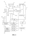
FIG. 1 is a schematic view of the framework of a power-saving electronic device for use with a computer motherboard in a "suspend to memory" state according to the present invention; -
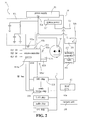
FIG. 2 is a schematic view of a preferred embodiment of the power-saving electronic device shown inFIG. 1 according to the present invention; -
FIG. 3 is a flowchart of processing a "suspend to memory" state event by the computer motherboard of the present invention; and -
FIG. 4 is a flowchart of processing awakening and resuming from the "suspend to memory" state by the computer motherboard of the present invention. - Please refer to
FIGs. 1 and2 . To facilitate description of the present invention and let persons skilled in the art gain insight into the present invention,FIGs. 1 and2 show components of acomputer motherboard 20 of the present invention on condition that the components are directly related to the present invention; in other words, irrelevant components of thecomputer motherboard 20 are omitted from the drawings. A power-savingelectronic device 10 for use with thecomputer motherboard 20 saves power as soon as thecomputer motherboard 20 enters a "suspend to memory" state. Thecomputer motherboard 20 is, for example, compatible with Advanced Configuration and Power Interface (ACPI) and capable of entering an S3 "suspend to RAM" state of ACPI (hereinafter referred to as ACPI S3). Persons skilled in the art are well aware that, upon its entry into ACPI S3, a conventional host computer is not effective in power saving, because some of the parts and components of the conventional host computer in ACPI S3 still consume standby power. For instance, a serial peripheral interface (SPI), read-only memory (ROM), LAN chip, audio chip, south bridge chip, and super input output (SIO) chip still consume standby power in ACPI S3. By contrast, as disclosed in the present invention, after thecomputer motherboard 20 equipped with the power-savingelectronic device 10 enters ACPI S3, the power-savingelectronic device 10 discontinues power supply to asouth bridge chip 205 and aSIO chip 203. In the situation where the same power source is shared by thesouth bridge chip 205, the SIOchip 203, a SPI ROM, a LAN chip, and an audio chip of thecomputer motherboard 20, the power-savingelectronic device 10 discontinues power supply to the SPI ROM, LAN chip, and audio chip as well. Meanwhile, power supply to the power-savingelectronic device 10, amemory controller 207, and amain memory 209 of thecomputer motherboard 20 remains unchanged. - Differences in standby power consumption between a conventional computer motherboard and the
computer motherboard 20 of the present invention, in ACPI S3, are shown in a comparative table as follows:Electronic Parts and Components Does a conventional computer motherboard consume standby power? Does the computer motherboard of the present invention consume standby power? memory controller yes yes main memory yes yes south bridge chip yes no SIO chip yes no LAN chip yes no audio chip yes no SPI ROM yes no power-saving electronic device 10no yes - According to the comparative table, the
computer motherboard 20 equipped with the power-savingelectronic device 10 reduces standby power consumption better than the conventional computer motherboard, andcomputer motherboard 20 equipped with the power-savingelectronic device 10 even overcomes a drawback of the prior art, that is, a conventional host computer fails to discontinue power supply to the south bridge chip and SIO chip in an S3 state. - The power-saving
electronic device 10 of the present invention reduces power consumed by thecomputer motherboard 20 operating in a "suspend to memory" state and waiting for awakening. For instance, configured for use with thecomputer motherboard 20 in ACPI S3, the power-savingelectronic device 10 comprises afirst device 101 and asecond device 103, as described in detail hereunder. - To work in conjunction with the power-saving
electronic device 10, thememory controller 207 andmain memory 209 of thecomputer motherboard 20 have a power source controllably switched between asecond standby power 30b and apower 30c by amemory power controller 211. Thememory power controller 211 is controlled by thesecond device 103. In an embodiment, thepower 30c is a power from asystem power 201, such as 5V, 3V, 5VSB, 3VSB, or 3.3VSB. In an embodiment, thesecond standby power 30b is a standby power from apower supply 30, such as 5V standby power, 3V standby power, or 3.3V standby power. In an embodiment, themain memory 209 is a single in-line memory module (SIMM), such as DDR, DDR2, or DDR3. - The primary function of the
first device 101 is to controllably determine whether afirst standby power 30a forms a close circuit or an open circuit with at least asouth bridge chip 205 and a super input output (SIO)chip 203 of thecomputer motherboard 20. Thefirst device 101 is a MOSFET, such as N-MOSFET or P-MOSFET. Thesecond device 103 controls the gate of the MOSFET, so as to controllably determine whether thefirst standby power 30a forms a close circuit or an open circuit with at least thesouth bridge chip 205 andSIO chip 203. - The
power supply 30 is an ATX power supply, for example. Thefirst standby power 30a is, for example, a standby power of the ATX power supply, such as 5V standby power, 3V standby power, or 3.3V standby power. For instance, the N-MOSFET features connection of one of a plurality of signal output ends of thesecond device 103 to the gate, connection of the drain to thefirst standby power 30a, and connection of the source to a plurality of pins of thesouth bridge chip 205 and theSIO chip 203. - The source of the N-MOSFET is further connected to a plurality of pins of the SPI ROM, the LAN chip, and the audio chip.
- Functions of the
second device 103 are described hereunder. Thesecond device 103 has first functionality: receiving apower switch signal 105a generated by apower switch 105; and enabling, upon receipt of thepower switch signal 105a, thefirst device 101 to control thefirst standby power 30a so as for thefirst standby power 30a in the control of thefirst device 101 to form a close circuit with at least thesouth bridge chip 205 andSIO chip 203. - In an embodiment, the
second device 103 essentially comprises a micro-controller 1031. Upon its receipt of thepower switch signal 105a, the micro-controller 1031 sends aconduction control signal 103a to the gate of the N-MOSFET 101 so as to bring the N-MOSFET 101 to an ON state, and in consequence thefirst standby power 30a forms a close circuit with at least thesouth bridge chip 205 andSIO chip 203. - Meanwhile, power supply to the SPI ROM, the LAN chip, and the audio chip resumes.
- The
second device 103 has second functionality: determining whether thecomputer motherboard 20 is in the "suspend to memory" state so as for thefirst standby power 30a to form an open circuit with at least thesouth bridge chip 205 andSIO chip 203 under the control of thefirst device 101 upon a positive determination; generating a memorypower control signal 103b and sending the memorypower control signal 103b to thememory power controller 211; and enabling thememory power controller 211 to switch thesecond standby power 30b to thememory controller 207 and themain memory 209 such that power supply to thememory controller 207 and themain memory 209 is maintained rather than interrupted. - An embodiment of the second function of the
second device 103 is described hereunder. The micro-controller 1031 receives signals, such as SLP_S3 or SLP_S5, from thesouth bridge chip 205 so as to determine whether thecomputer motherboard 20 is in ACPI S3, and, upon a positive determination, instructs the N-MOSFET 101 to hibernate so as for thefirst standby power 30a to form an open circuit with at least thesouth bridge chip 205 andSIO chip 203. - Meanwhile, the micro-controller 1031 determines whether the
computer motherboard 20 is in ACPI S3 and sends, upon a positive determination, the memorypower control signal 103b to thememory power controller 211. Upon its receipt of the memorypower control signal 103b, thememory power controller 211 begins switching, thereby allowing thesecond standby power 30b to form a close circuit with thememory controller 207 andmain memory 209. Hence, during ACPI S3, power supply to thememory controller 207 and themain memory 209 is maintained rather than interrupted. - In addition, the SPI ROM, the LAN chip, and the audio chip form an open circuit with the
first standby power 30a. - The
second device 103 has a third function, that is, after receiving thepower switch signal 105a, thesecond device 103 reproduces thepower switch signal 105a and sends apower switch signal 105a' thus reproduced to theSIO chip 203 of thecomputer motherboard 20. - An embodiment of the third function of the
second device 103 is described hereunder. Upon receipt of thepower switch signal 105a by the micro-controller 1031, a built-in power switch signal reproducing circuit (not shown) provided in the micro-controller 1031 reproduces thepower switch signal 105a and sends apower switch signal 105a' thus reproduced to theSIO chip 203 of thecomputer motherboard 20. Alternatively, upon its receipt of thepower switch signal 105a, the micro-controller 1031 executes a program to control the voltage level at an output port of the micro-controller 1031 so as for the thus-reproducedpower switch signal 105a' to be sent from the output port to theSIO chip 203 of thecomputer motherboard 20. - The
computer motherboard 20 receiving power from thefirst standby power 30a still generates signal RSMRST (the signal RSMRST is, for example, generated by thesecond device 103 or the SIO chip 203) and sends the signal RSMRST to thesouth bridge chip 205. Thesecond device 103 awaits during a predetermined period of time, that is, the time thesecond device 103 takes to wait for completion of generation of the signal RSMRST by thecomputer motherboard 20, such as 100ms. - After bringing the N-
MOSFET 101 to an ON state, the micro-controller 1031 awaits for a predetermined period of time, that is, 100ms. At the end of the predetermined period of 100ms (that is, the moment when thecomputer motherboard 20 has finished generating the signal RSMRST), the micro-controller 1031 generates thepower switch signal 105a' and sends thepower switch signal 105a' thus generated to theSIO chip 203. Upon receipt of thepower switch signal 105a' by theSIO chip 203, thecomputer motherboard 20 executes the follow-up procedure of awakening from S3 state to S0 state. - The N-MOSFET in the power on state is likely to be overloaded and burned out when subjected to instantaneous overcurrent. To avoid the mishap, the present invention discloses a soft
start circuit unit 1033. The softstart circuit unit 1033 can adopt a conventional circuit. - To increase a control voltage with a view to using low-cost field-effect transistors (FET), the present invention discloses a charge
pump circuit unit 1035. The chargepump circuit unit 1035 can adopt a conventional circuit. - The
second device 103 of the present invention can be implemented as an application-specific integrated circuit (ASIC). - The
south bridge chip 205, theSIO chip 203, thememory controller 207, and themain memory 209 can adopt conventional components. - The
memory power controller 211 can adopt a conventional electronic switch or a conventional electronic switching circuit. - The power-saving
electronic device 10 of the present invention is disposed on thecomputer motherboard 20; alternatively, the power-savingelectronic device 10 of the present invention is integrated with theSIO chip 203 of thecomputer motherboard 20. - In an embodiment, the
system power 201 is a power source of an ATX power source interface (connector) for use with thecomputer motherboard 20, and the ATX power source interface is connected to thepower supply 30 via a cable. - A built-in
memory 1031 a of the micro-controller 1031 functions as firmware. A code required for execution of the first, second, and third functions of thesecond device 103 is stored in the built-inmemory 1031a. The micro-controller 1031 is connected to thesouth bridge chip 205 via an SM bus; hence, new firmware for the micro-controller 1031 is updated via the SM bus. - To enable the power-saving
electronic device 10 to discontinue power supply to thesouth bridge chip 205 andSIO chip 203, acode 40a is added to a basic input and output system (BIOS) 40 of thecomputer motherboard 20 of the present invention. Thecode 40a is required for storing a flag in a memory unit whenever thecomputer motherboard 20 is in a "suspend to memory" state. Thecode 40a is required for checking the flag whenever power supply to thesouth bridge chip 205 andSIO chip 203 resumes, so as to determine whether a preceding state of thecomputer motherboard 20 is the "suspend to memory" state and execute, upon a positive determination, awakening and resuming from the "suspend to memory" state. - Referring to
FIG. 3 , once a "suspend to memory" state event (e.g., ACPI S3 event) occurs to thecomputer motherboard 20, a window operating system (e.g., Windows™ of Microsoft™) stores related data in the main memory 209 (S401). Then, the flag is stored in thememory unit 210 by means of thecode 40a in the BIOS 40 (S402). Afterward, the window operating system informs thesouth bridge chip 205 of the occurrence of the "suspend to memory" state event (S403). In response to the notification, thesouth bridge chip 205 soft shuts down thepower supply 30, but power supply to thesouth bridge chip 205, theSIO chip 203, the SPI ROM, the LAN chip, and the audio chip remains uninterrupted (S404). Then, the power-savingelectronic device 10 performs the aforesaid power-saving functionality, so as to discontinue power supply to thesouth bridge chip 205, theSIO chip 203, the SPI ROM, the LAN chip, and the audio chip. Thememory power controller 211 switches to thesecond standby power 30b by the memorypower control signal 103b such that power supply to thememory controller 207 and themain memory 209 is maintained rather than interrupted (S405). - Afterward, the
computer motherboard 20 finalizes the S3 state (S406), - The steps S401, S403, S404, and S406 illustrated with
FIG. 3 are attributable to the prior art related to a known way to cope with an S3 event. It should be noted that, compared to the prior art, the present invention includes new steps, such as S402 and S405, to enhance the power-saving functionality of thecomputer motherboard 20 and enable recordation of occurrence of an S3 event to thecomputer motherboard 20. - Referring to
FIG. 4 , once a user presses thepower switch 105, an event of awakening from a "suspend to memory" state and reuming occurs to the computer motherboard 20 (for example, an event of "awakening from ACPI S3 to S0" occurs to the computer motherboard 20); meanwhile, the power-savingelectronic device 10 performs the aforesaid power-restoring functionality, so as to resume power supply to thesouth bridge chip 205, theSIO chip 203, the SPI ROM, the LAN chip, and the audio chip (S501). Furthermore, in S501, the power-savingelectronic device 10 enables switching of thememory power controller 211 such that thepower 30c forms a close circuit with thememory controller 207 and themain memory 209. Then, thesouth bridge chip 205 enters a power on state (S502). Afterward, the flag is read by thecode 40a in theBIOS 40 to check and determine whether the flag is set and determine, upon a determination of a TRUTH result (i.e., the flag is set), whether a preceding state of thecomputer motherboard 20 is the "suspend to memory" state. Then, thecode 40a enables thesouth bridge chip 205 to execute an event of awakening from the "suspend to memory" state (S503). Furthermore, in S503, thecode 40a clears the flag value. Afterward, the window operating system reads themain memory 209 and restores related data (S504). Lastly, thecomputer motherboard 20 awakens and resumes from the "suspend to memory" state (S505). - The steps S502, S504, and S505 illustrated with
FIG. 4 are attributable to the prior art related to a known way to cope with an event of awakening from a "suspend to memory" state and restoring. It should be noted that, compared to the prior art, the present invention includes new steps, such as S501 and S503, so as to allow thecomputer motherboard 20 to awaken from a "suspend to memory" state and resume even after power supply to thesouth bridge chip 205 andSIO chip 203 has been interrupted. - The
memory unit 210 is a built-in CMOS memory of thecomputer motherboard 20, a built-in embedded controller (EC) of a notebook computer, or an internal register of thesecond device 103. - As disclosed in the present invention, a power-saving electronic device for use with a computer motherboard is capable of compelling interruption of power supply to a south bridge chip and a super input output (SIO) chip of the computer motherboard in a "suspend to memory" state so as to save power, and yet enables the computer motherboard to remain capable of awakening and resuming from the S3 state, which are the advantages and characteristics of the present invention.
- The above description serves to expound preferred embodiments of the present invention rather than limit the scope of application of the present invention. Persons skilled in the art should be able to make obvious changes or modification of the present invention without departing from the substantive disclosure of the present invention.
Claims (10)
- A computer motherboard, comprising:a south bridge chip (205) electrically connected to a first device (101);a super input output - SIO - chip (203) electrically connected to the first device (101);the first device controlled by a second device (103) and configured to controllably form a closed circuit or an open circuit between a first standby power (30a) and the south bridge chip and SIO chip;the second device configured to determine whether the computer motherboard is in the "suspend to memory" state so as to form an open circuit between the first standby power and the south bridge chip and SIO chip under control of the first device upon a positive determination, and configured to determine whether the computer motherboard is in the "suspend to memory" state so as to form a closed circuit between a second standby power (30b) and a memory controller (207) and a main memory (209) of the computer motherboard upon a positive determination, and configured to receive a power switch signal (105a) generated by a power switch (105), and configured to enable to form a closed circuit between the first standby power and the south bridge chip and SIO chip under control of the first device upon receipt of the power switch signal; andthe computer motherboard being configured to comprise a basic input and output system (BIOS) comprising code for: storing a flag in a memory unit (210) whenever the computer motherboard is in the "suspend to memory" state; checking the flag and determining, as soon as power supply to the south bridge chip and the SIO chip resumes, whether a preceding state of the computer motherboard is the "suspend to memory" state; and executing , upon a positive determination, awakening and resuming from the "suspend to memory" state.
- The computer motherboard of claim 1, wherein the "suspend to memory" state is an S3 state of Advanced Configuration and Power Interface (ACPI).
- The computer motherboard of claim 1, further comprising a memory power controller (211) for switching the power source of the memory controller and the main memory, wherein, when the computer motherboard is in the "suspend to memory" state, the memory power controller is configured for being controlled by the second device and configured for switching the power source of the memory controller and the main memory to the second standby power.
- The computer motherboard of claim 1, further comprising a charge pump circuit unit (1035).
- The computer motherboard of claim 1, further comprising a soft start circuit unit (1030).
- The computer motherboard of claim 1, wherein the first device and the second device are integrated with the super input output (SIO) chip.
- The computer motherboard of claim 1, wherein the second device is a micro-controller or an application-specific integrated circuit (ASIC).
- The computer motherboard of claim 1, wherein the second device is configured to reproduce the power switch signal and to send a power switch signal (105a') thus reproduced to the SIO chip of the computer motherboard.
- The computer motherboard of claim 8, wherein the second device is configured to reproduce the power switch signal and to send the power switch signal thus reproduced to the SIO chip, by a means of executing instruction codes to control a voltage level at an output port of the second device.
- The computer motherboard of claim 1, wherein the memory unit is a built-in CMOS memory of the computer motherboard, a built-in embedded controller (EC) of a notebook computer, or an internal register of the second device.
Applications Claiming Priority (1)
| Application Number | Priority Date | Filing Date | Title |
|---|---|---|---|
| US12/422,118 US8132032B2 (en) | 2009-04-10 | 2009-04-10 | Electronic device for reducing power consumption during sleep mode of computer motherboard and motherboard thereof |
Publications (3)
| Publication Number | Publication Date |
|---|---|
| EP2239647A2 EP2239647A2 (en) | 2010-10-13 |
| EP2239647A3 EP2239647A3 (en) | 2011-10-26 |
| EP2239647B1 true EP2239647B1 (en) | 2014-11-26 |
Family
ID=41335449
Family Applications (1)
| Application Number | Title | Priority Date | Filing Date |
|---|---|---|---|
| EP09168080.1A Active EP2239647B1 (en) | 2009-04-10 | 2009-08-18 | Motherboard with electronic device for reducing power consumption during sleep mode of computer motherboard |
Country Status (6)
| Country | Link |
|---|---|
| US (1) | US8132032B2 (en) |
| EP (1) | EP2239647B1 (en) |
| JP (1) | JP5165652B2 (en) |
| CN (1) | CN101859173B (en) |
| DE (1) | DE202009011250U1 (en) |
| TW (2) | TWI464571B (en) |
Families Citing this family (31)
| Publication number | Priority date | Publication date | Assignee | Title |
|---|---|---|---|---|
| DE102008054601A1 (en) * | 2008-12-14 | 2010-06-24 | Getac Technology Corp. | Hard disk temperature monitor and hard disk temperature monitoring method |
| US20100332870A1 (en) * | 2009-06-25 | 2010-12-30 | Micro-Star International Co., Ltd. | Electronic device for reducing power consumption of computer motherboard and motherboard thereof |
| CN102136791A (en) * | 2010-01-22 | 2011-07-27 | 环旭电子股份有限公司 | Power supply control circuit |
| CN102314209B (en) * | 2010-07-06 | 2014-08-27 | 南京亚士德科技有限公司 | Control circuit of mainboard power supply |
| TWM412423U (en) * | 2010-08-13 | 2011-09-21 | Micro Star Int Co Ltd | Computer motherboard for reducing power consumption during sleep mode |
| CN201780549U (en) * | 2010-08-16 | 2011-03-30 | 鸿富锦精密工业(深圳)有限公司 | Multi-status switch control device and system |
| CN102375522A (en) * | 2010-08-27 | 2012-03-14 | 鸿富锦精密工业(深圳)有限公司 | Power supply system of electronic device |
| CN102566656A (en) * | 2010-12-20 | 2012-07-11 | 鸿富锦精密工业(深圳)有限公司 | Main board for computer |
| US10042650B2 (en) * | 2011-03-23 | 2018-08-07 | Lenovo (Beijing) Co., Ltd. | Computer startup method, startup apparatus, state transition method and state transition apparatus |
| CN102799252A (en) * | 2011-05-26 | 2012-11-28 | 华硕电脑股份有限公司 | Computer device and power generator thereof |
| CN102360244A (en) * | 2011-09-28 | 2012-02-22 | 深圳市卓怡恒通电脑科技有限公司 | Standby method for lengthening standby time of computer |
| TWI459289B (en) * | 2012-01-03 | 2014-11-01 | Sk Hynix Inc | Embedded memory card control system with no power sleep mode and its embedded memory card |
| CN103197750B (en) * | 2012-01-09 | 2015-10-28 | 爱思开海力士有限公司 | Embedded memory card control system and embedded memory card thereof |
| JP5975662B2 (en) * | 2012-02-06 | 2016-08-23 | キヤノン株式会社 | Image forming apparatus and image forming apparatus control method |
| CN103455127B (en) * | 2012-05-29 | 2016-02-03 | 国基电子(上海)有限公司 | Apparatus for monitoring power supply, electronic installation and method for monitoring power supply thereof |
| CN103885861A (en) * | 2012-12-22 | 2014-06-25 | 鸿富锦精密工业(武汉)有限公司 | Testing device for start-up test of electronic device |
| US9268699B2 (en) * | 2013-06-03 | 2016-02-23 | Samsung Electronics Co., Ltd. | Dynamic cache allocation in a solid state drive environment |
| CN104345850B (en) * | 2013-08-09 | 2018-05-08 | 瑞祺电通股份有限公司 | Intelligent automatic boot device |
| US9891696B2 (en) | 2014-10-03 | 2018-02-13 | Google Llc | Intelligent device wakeup |
| TWI547796B (en) * | 2014-11-13 | 2016-09-01 | 鴻海精密工業股份有限公司 | Motherboard supply circuit |
| CN105652995A (en) * | 2014-11-13 | 2016-06-08 | 鸿富锦精密工业(武汉)有限公司 | Mainboard power supply circuit |
| CN105700654B (en) * | 2014-11-28 | 2020-04-17 | 鸿富锦精密工业(武汉)有限公司 | Electronic equipment and circuit for preventing live operation of mainboard |
| CN104539018B (en) * | 2014-12-26 | 2017-12-22 | 英华达(上海)科技有限公司 | Electronic installation and electricity saving method |
| TWI563373B (en) | 2015-03-20 | 2016-12-21 | Giga Byte Tech Co Ltd | Motherboard with backup power |
| CN106155250B (en) * | 2015-04-17 | 2019-08-06 | 鸿富锦精密工业(武汉)有限公司 | computer recovery circuit |
| CN107807728B (en) * | 2016-09-09 | 2020-07-21 | 佛山市顺德区顺达电脑厂有限公司 | Shutdown discharge system |
| KR101972917B1 (en) * | 2018-12-26 | 2019-04-26 | (주)엠텍정보 | A power saving method of a computer system by automatically controlling registry setting values according to the idle resource |
| CN110570644B (en) * | 2019-09-24 | 2020-09-22 | 广州华端科技有限公司 | Remote control device |
| TWI768373B (en) * | 2020-06-12 | 2022-06-21 | 宏碁股份有限公司 | Power control method for a memory storage device and a memory storage system |
| TWI788759B (en) * | 2020-08-27 | 2023-01-01 | 瑞昱半導體股份有限公司 | Docking station for power management |
| TWI821949B (en) * | 2022-03-17 | 2023-11-11 | 茂達電子股份有限公司 | Power saving system of battery charger |
Family Cites Families (18)
| Publication number | Priority date | Publication date | Assignee | Title |
|---|---|---|---|---|
| JPH10149236A (en) * | 1996-11-15 | 1998-06-02 | Nec Corp | Method for recovering hibernation |
| JP3943665B2 (en) * | 1997-09-01 | 2007-07-11 | 株式会社東芝 | Sleep control method and event notification method |
| JPH11161385A (en) * | 1997-11-28 | 1999-06-18 | Toshiba Corp | Computer system and system state control method thereof |
| US6308278B1 (en) * | 1997-12-29 | 2001-10-23 | Intel Corporation | Supplying standby voltage to memory and wakeup circuitry to wake a computer from a low power mode |
| JP3851736B2 (en) * | 1999-01-12 | 2006-11-29 | 株式会社東芝 | Electronic device and system startup method |
| TW448352B (en) * | 1999-09-06 | 2001-08-01 | Via Tech Inc | Power-saving device and method for suspend to RAM |
| JP2003196096A (en) * | 2001-12-07 | 2003-07-11 | Internatl Business Mach Corp <Ibm> | Computer system, its starting control method and program |
| JP3777136B2 (en) * | 2002-04-01 | 2006-05-24 | インターナショナル・ビジネス・マシーンズ・コーポレーション | Computer device, data dead copy method, program, and computer device operating method |
| TWI224728B (en) * | 2002-10-03 | 2004-12-01 | Via Tech Inc | Method and related apparatus for maintaining stored data of a dynamic random access memory |
| US20050044449A1 (en) * | 2003-08-19 | 2005-02-24 | Dunstan Robert A. | Power button and device wake event processing methods in the absence of AC power |
| US7089433B2 (en) * | 2003-09-26 | 2006-08-08 | Dell Products L.P. | Method and system for operating system quiescent state |
| US8194692B2 (en) * | 2004-11-22 | 2012-06-05 | Via Technologies, Inc. | Apparatus with and a method for a dynamic interface protocol |
| JP2007133564A (en) * | 2005-11-09 | 2007-05-31 | Canon Inc | Information processing device |
| TWI303763B (en) * | 2006-01-25 | 2008-12-01 | Via Tech Inc | Device and method for controlling refresh rate of memory |
| JP2007249660A (en) * | 2006-03-16 | 2007-09-27 | Toshiba Corp | Information processing apparatus and system state control method |
| JP4459946B2 (en) * | 2006-11-21 | 2010-04-28 | レノボ・シンガポール・プライベート・リミテッド | Portable computer and operation mode control method |
| TWI385507B (en) * | 2007-08-15 | 2013-02-11 | Via Tech Inc | Method and device for adjusting data transmission rate and computer system with the same function |
| US20090106573A1 (en) * | 2007-10-18 | 2009-04-23 | Inventec Corporation | Power saving method |
-
2009
- 2009-04-10 US US12/422,118 patent/US8132032B2/en active Active
- 2009-06-17 TW TW098120188A patent/TWI464571B/en active
- 2009-06-26 TW TW098121493A patent/TW201003378A/en unknown
- 2009-08-13 CN CN2009101657804A patent/CN101859173B/en active Active
- 2009-08-13 JP JP2009187770A patent/JP5165652B2/en active Active
- 2009-08-18 EP EP09168080.1A patent/EP2239647B1/en active Active
- 2009-08-18 DE DE202009011250U patent/DE202009011250U1/en not_active Expired - Lifetime
Also Published As
| Publication number | Publication date |
|---|---|
| US8132032B2 (en) | 2012-03-06 |
| EP2239647A3 (en) | 2011-10-26 |
| DE202009011250U1 (en) | 2009-11-19 |
| CN101859173B (en) | 2013-06-26 |
| EP2239647A2 (en) | 2010-10-13 |
| US20100262849A1 (en) | 2010-10-14 |
| JP2010250792A (en) | 2010-11-04 |
| JP5165652B2 (en) | 2013-03-21 |
| TW201003378A (en) | 2010-01-16 |
| TWI464571B (en) | 2014-12-11 |
| TW201037504A (en) | 2010-10-16 |
| CN101859173A (en) | 2010-10-13 |
Similar Documents
| Publication | Publication Date | Title |
|---|---|---|
| US8132032B2 (en) | Electronic device for reducing power consumption during sleep mode of computer motherboard and motherboard thereof | |
| EP2267575B1 (en) | Electronic device for reducing power consumption of computer motherboard and motherboard thereof | |
| CN102566739B (en) | Multi-core processor system and its dynamic power management method and control device | |
| CN101470509B (en) | Computer system control method, computer system and notebook computer | |
| US10817043B2 (en) | System and method for entering and exiting sleep mode in a graphics subsystem | |
| EP2843502B1 (en) | Information processing device, information processing method, and program | |
| US8762757B2 (en) | Power management method and device thereof | |
| JP3168471U (en) | Computer motherboard capable of reducing power consumption while suspended | |
| US8195966B2 (en) | Electronic device for reducing power consumption during off of computer motherboard | |
| KR20100090513A (en) | Low power system-on-chip | |
| CN1303035A (en) | Power controlling circuit possessing computer system with several power source management state | |
| US12504806B2 (en) | Mechanism for saving power on a bus interface | |
| KR100392451B1 (en) | Portable computer system and controlling method thereof | |
| US20120047381A1 (en) | Control Device, Main Board and Computer | |
| CN103970248A (en) | power management circuit and method and computer system | |
| TW200928982A (en) | Host device and computer system for reducing power consumption in graphic cards | |
| TWI783163B (en) | Power control device, computer system and related power control method | |
| CN101408792A (en) | Power management device and management method thereof | |
| KR102244643B1 (en) | Switching mode power supply built-in standby power cut-off apparatus and method | |
| EP2821880B1 (en) | Power control system and method thereof | |
| CN101751110B (en) | Electronic device for reducing shutdown power consumption of computer mainboard and computer mainboard | |
| TWI501073B (en) | Computer device and power supply method for universal port module | |
| TW201416847A (en) | Computer device and wake-up method therefore |
Legal Events
| Date | Code | Title | Description |
|---|---|---|---|
| PUAI | Public reference made under article 153(3) epc to a published international application that has entered the european phase |
Free format text: ORIGINAL CODE: 0009012 |
|
| AK | Designated contracting states |
Kind code of ref document: A2 Designated state(s): AT BE BG CH CY CZ DE DK EE ES FI FR GB GR HR HU IE IS IT LI LT LU LV MC MK MT NL NO PL PT RO SE SI SK SM TR |
|
| AX | Request for extension of the european patent |
Extension state: AL BA RS |
|
| RAP1 | Party data changed (applicant data changed or rights of an application transferred) |
Owner name: MICRO-STAR INTERNATIONAL CO., LTD. |
|
| RIN1 | Information on inventor provided before grant (corrected) |
Inventor name: YEH, CHUN-TE Inventor name: CHEN, CHUNG-WEN |
|
| PUAL | Search report despatched |
Free format text: ORIGINAL CODE: 0009013 |
|
| AK | Designated contracting states |
Kind code of ref document: A3 Designated state(s): AT BE BG CH CY CZ DE DK EE ES FI FR GB GR HR HU IE IS IT LI LT LU LV MC MK MT NL NO PL PT RO SE SI SK SM TR |
|
| AX | Request for extension of the european patent |
Extension state: AL BA RS |
|
| RIC1 | Information provided on ipc code assigned before grant |
Ipc: G06F 1/32 20060101AFI20110922BHEP |
|
| 17P | Request for examination filed |
Effective date: 20120329 |
|
| 17Q | First examination report despatched |
Effective date: 20120824 |
|
| GRAP | Despatch of communication of intention to grant a patent |
Free format text: ORIGINAL CODE: EPIDOSNIGR1 |
|
| INTG | Intention to grant announced |
Effective date: 20140704 |
|
| GRAS | Grant fee paid |
Free format text: ORIGINAL CODE: EPIDOSNIGR3 |
|
| GRAA | (expected) grant |
Free format text: ORIGINAL CODE: 0009210 |
|
| AK | Designated contracting states |
Kind code of ref document: B1 Designated state(s): AT BE BG CH CY CZ DE DK EE ES FI FR GB GR HR HU IE IS IT LI LT LU LV MC MK MT NL NO PL PT RO SE SI SK SM TR |
|
| REG | Reference to a national code |
Ref country code: GB Ref legal event code: FG4D |
|
| REG | Reference to a national code |
Ref country code: CH Ref legal event code: EP |
|
| REG | Reference to a national code |
Ref country code: AT Ref legal event code: REF Ref document number: 698541 Country of ref document: AT Kind code of ref document: T Effective date: 20141215 |
|
| REG | Reference to a national code |
Ref country code: IE Ref legal event code: FG4D |
|
| REG | Reference to a national code |
Ref country code: DE Ref legal event code: R096 Ref document number: 602009027939 Country of ref document: DE Effective date: 20150108 |
|
| REG | Reference to a national code |
Ref country code: NL Ref legal event code: VDEP Effective date: 20141126 |
|
| REG | Reference to a national code |
Ref country code: AT Ref legal event code: MK05 Ref document number: 698541 Country of ref document: AT Kind code of ref document: T Effective date: 20141126 |
|
| REG | Reference to a national code |
Ref country code: LT Ref legal event code: MG4D |
|
| PG25 | Lapsed in a contracting state [announced via postgrant information from national office to epo] |
Ref country code: PT Free format text: LAPSE BECAUSE OF FAILURE TO SUBMIT A TRANSLATION OF THE DESCRIPTION OR TO PAY THE FEE WITHIN THE PRESCRIBED TIME-LIMIT Effective date: 20150326 Ref country code: ES Free format text: LAPSE BECAUSE OF FAILURE TO SUBMIT A TRANSLATION OF THE DESCRIPTION OR TO PAY THE FEE WITHIN THE PRESCRIBED TIME-LIMIT Effective date: 20141126 Ref country code: IS Free format text: LAPSE BECAUSE OF FAILURE TO SUBMIT A TRANSLATION OF THE DESCRIPTION OR TO PAY THE FEE WITHIN THE PRESCRIBED TIME-LIMIT Effective date: 20150326 Ref country code: FI Free format text: LAPSE BECAUSE OF FAILURE TO SUBMIT A TRANSLATION OF THE DESCRIPTION OR TO PAY THE FEE WITHIN THE PRESCRIBED TIME-LIMIT Effective date: 20141126 Ref country code: NO Free format text: LAPSE BECAUSE OF FAILURE TO SUBMIT A TRANSLATION OF THE DESCRIPTION OR TO PAY THE FEE WITHIN THE PRESCRIBED TIME-LIMIT Effective date: 20150226 Ref country code: NL Free format text: LAPSE BECAUSE OF FAILURE TO SUBMIT A TRANSLATION OF THE DESCRIPTION OR TO PAY THE FEE WITHIN THE PRESCRIBED TIME-LIMIT Effective date: 20141126 Ref country code: LT Free format text: LAPSE BECAUSE OF FAILURE TO SUBMIT A TRANSLATION OF THE DESCRIPTION OR TO PAY THE FEE WITHIN THE PRESCRIBED TIME-LIMIT Effective date: 20141126 |
|
| PG25 | Lapsed in a contracting state [announced via postgrant information from national office to epo] |
Ref country code: AT Free format text: LAPSE BECAUSE OF FAILURE TO SUBMIT A TRANSLATION OF THE DESCRIPTION OR TO PAY THE FEE WITHIN THE PRESCRIBED TIME-LIMIT Effective date: 20141126 Ref country code: CY Free format text: LAPSE BECAUSE OF FAILURE TO SUBMIT A TRANSLATION OF THE DESCRIPTION OR TO PAY THE FEE WITHIN THE PRESCRIBED TIME-LIMIT Effective date: 20141126 Ref country code: SE Free format text: LAPSE BECAUSE OF FAILURE TO SUBMIT A TRANSLATION OF THE DESCRIPTION OR TO PAY THE FEE WITHIN THE PRESCRIBED TIME-LIMIT Effective date: 20141126 Ref country code: HR Free format text: LAPSE BECAUSE OF FAILURE TO SUBMIT A TRANSLATION OF THE DESCRIPTION OR TO PAY THE FEE WITHIN THE PRESCRIBED TIME-LIMIT Effective date: 20141126 Ref country code: LV Free format text: LAPSE BECAUSE OF FAILURE TO SUBMIT A TRANSLATION OF THE DESCRIPTION OR TO PAY THE FEE WITHIN THE PRESCRIBED TIME-LIMIT Effective date: 20141126 |
|
| PG25 | Lapsed in a contracting state [announced via postgrant information from national office to epo] |
Ref country code: DK Free format text: LAPSE BECAUSE OF FAILURE TO SUBMIT A TRANSLATION OF THE DESCRIPTION OR TO PAY THE FEE WITHIN THE PRESCRIBED TIME-LIMIT Effective date: 20141126 Ref country code: EE Free format text: LAPSE BECAUSE OF FAILURE TO SUBMIT A TRANSLATION OF THE DESCRIPTION OR TO PAY THE FEE WITHIN THE PRESCRIBED TIME-LIMIT Effective date: 20141126 Ref country code: RO Free format text: LAPSE BECAUSE OF FAILURE TO SUBMIT A TRANSLATION OF THE DESCRIPTION OR TO PAY THE FEE WITHIN THE PRESCRIBED TIME-LIMIT Effective date: 20141126 Ref country code: SK Free format text: LAPSE BECAUSE OF FAILURE TO SUBMIT A TRANSLATION OF THE DESCRIPTION OR TO PAY THE FEE WITHIN THE PRESCRIBED TIME-LIMIT Effective date: 20141126 Ref country code: CZ Free format text: LAPSE BECAUSE OF FAILURE TO SUBMIT A TRANSLATION OF THE DESCRIPTION OR TO PAY THE FEE WITHIN THE PRESCRIBED TIME-LIMIT Effective date: 20141126 |
|
| REG | Reference to a national code |
Ref country code: DE Ref legal event code: R097 Ref document number: 602009027939 Country of ref document: DE |
|
| PG25 | Lapsed in a contracting state [announced via postgrant information from national office to epo] |
Ref country code: PL Free format text: LAPSE BECAUSE OF FAILURE TO SUBMIT A TRANSLATION OF THE DESCRIPTION OR TO PAY THE FEE WITHIN THE PRESCRIBED TIME-LIMIT Effective date: 20141126 |
|
| PLBE | No opposition filed within time limit |
Free format text: ORIGINAL CODE: 0009261 |
|
| STAA | Information on the status of an ep patent application or granted ep patent |
Free format text: STATUS: NO OPPOSITION FILED WITHIN TIME LIMIT |
|
| 26N | No opposition filed |
Effective date: 20150827 |
|
| PG25 | Lapsed in a contracting state [announced via postgrant information from national office to epo] |
Ref country code: IT Free format text: LAPSE BECAUSE OF FAILURE TO SUBMIT A TRANSLATION OF THE DESCRIPTION OR TO PAY THE FEE WITHIN THE PRESCRIBED TIME-LIMIT Effective date: 20141126 |
|
| PG25 | Lapsed in a contracting state [announced via postgrant information from national office to epo] |
Ref country code: SI Free format text: LAPSE BECAUSE OF FAILURE TO SUBMIT A TRANSLATION OF THE DESCRIPTION OR TO PAY THE FEE WITHIN THE PRESCRIBED TIME-LIMIT Effective date: 20141126 |
|
| PG25 | Lapsed in a contracting state [announced via postgrant information from national office to epo] |
Ref country code: LU Free format text: LAPSE BECAUSE OF FAILURE TO SUBMIT A TRANSLATION OF THE DESCRIPTION OR TO PAY THE FEE WITHIN THE PRESCRIBED TIME-LIMIT Effective date: 20150818 Ref country code: MC Free format text: LAPSE BECAUSE OF FAILURE TO SUBMIT A TRANSLATION OF THE DESCRIPTION OR TO PAY THE FEE WITHIN THE PRESCRIBED TIME-LIMIT Effective date: 20141126 |
|
| REG | Reference to a national code |
Ref country code: CH Ref legal event code: PL |
|
| PG25 | Lapsed in a contracting state [announced via postgrant information from national office to epo] |
Ref country code: LI Free format text: LAPSE BECAUSE OF NON-PAYMENT OF DUE FEES Effective date: 20150831 Ref country code: CH Free format text: LAPSE BECAUSE OF NON-PAYMENT OF DUE FEES Effective date: 20150831 |
|
| REG | Reference to a national code |
Ref country code: FR Ref legal event code: PLFP Year of fee payment: 8 |
|
| REG | Reference to a national code |
Ref country code: IE Ref legal event code: MM4A |
|
| PG25 | Lapsed in a contracting state [announced via postgrant information from national office to epo] |
Ref country code: IE Free format text: LAPSE BECAUSE OF NON-PAYMENT OF DUE FEES Effective date: 20150818 |
|
| PG25 | Lapsed in a contracting state [announced via postgrant information from national office to epo] |
Ref country code: MT Free format text: LAPSE BECAUSE OF FAILURE TO SUBMIT A TRANSLATION OF THE DESCRIPTION OR TO PAY THE FEE WITHIN THE PRESCRIBED TIME-LIMIT Effective date: 20141126 |
|
| REG | Reference to a national code |
Ref country code: FR Ref legal event code: PLFP Year of fee payment: 9 |
|
| PG25 | Lapsed in a contracting state [announced via postgrant information from national office to epo] |
Ref country code: BG Free format text: LAPSE BECAUSE OF FAILURE TO SUBMIT A TRANSLATION OF THE DESCRIPTION OR TO PAY THE FEE WITHIN THE PRESCRIBED TIME-LIMIT Effective date: 20141126 Ref country code: SM Free format text: LAPSE BECAUSE OF FAILURE TO SUBMIT A TRANSLATION OF THE DESCRIPTION OR TO PAY THE FEE WITHIN THE PRESCRIBED TIME-LIMIT Effective date: 20141126 Ref country code: HU Free format text: LAPSE BECAUSE OF FAILURE TO SUBMIT A TRANSLATION OF THE DESCRIPTION OR TO PAY THE FEE WITHIN THE PRESCRIBED TIME-LIMIT; INVALID AB INITIO Effective date: 20090818 |
|
| PG25 | Lapsed in a contracting state [announced via postgrant information from national office to epo] |
Ref country code: GR Free format text: LAPSE BECAUSE OF FAILURE TO SUBMIT A TRANSLATION OF THE DESCRIPTION OR TO PAY THE FEE WITHIN THE PRESCRIBED TIME-LIMIT Effective date: 20141126 |
|
| PG25 | Lapsed in a contracting state [announced via postgrant information from national office to epo] |
Ref country code: TR Free format text: LAPSE BECAUSE OF FAILURE TO SUBMIT A TRANSLATION OF THE DESCRIPTION OR TO PAY THE FEE WITHIN THE PRESCRIBED TIME-LIMIT Effective date: 20141126 |
|
| PG25 | Lapsed in a contracting state [announced via postgrant information from national office to epo] |
Ref country code: BE Free format text: LAPSE BECAUSE OF FAILURE TO SUBMIT A TRANSLATION OF THE DESCRIPTION OR TO PAY THE FEE WITHIN THE PRESCRIBED TIME-LIMIT Effective date: 20141126 |
|
| REG | Reference to a national code |
Ref country code: FR Ref legal event code: PLFP Year of fee payment: 10 |
|
| PG25 | Lapsed in a contracting state [announced via postgrant information from national office to epo] |
Ref country code: MK Free format text: LAPSE BECAUSE OF FAILURE TO SUBMIT A TRANSLATION OF THE DESCRIPTION OR TO PAY THE FEE WITHIN THE PRESCRIBED TIME-LIMIT Effective date: 20141126 |
|
| PGFP | Annual fee paid to national office [announced via postgrant information from national office to epo] |
Ref country code: GB Payment date: 20250602 Year of fee payment: 17 |
|
| PGFP | Annual fee paid to national office [announced via postgrant information from national office to epo] |
Ref country code: FR Payment date: 20250520 Year of fee payment: 17 |
|
| PGFP | Annual fee paid to national office [announced via postgrant information from national office to epo] |
Ref country code: DE Payment date: 20250522 Year of fee payment: 17 |