EP2237331B1 - Light-emitting device and illuminating device - Google Patents
Light-emitting device and illuminating device Download PDFInfo
- Publication number
- EP2237331B1 EP2237331B1 EP08863988.5A EP08863988A EP2237331B1 EP 2237331 B1 EP2237331 B1 EP 2237331B1 EP 08863988 A EP08863988 A EP 08863988A EP 2237331 B1 EP2237331 B1 EP 2237331B1
- Authority
- EP
- European Patent Office
- Prior art keywords
- light emitting
- light
- reflecting portion
- sub
- base
- Prior art date
- Legal status (The legal status is an assumption and is not a legal conclusion. Google has not performed a legal analysis and makes no representation as to the accuracy of the status listed.)
- Not-in-force
Links
Images



Classifications
-
- H—ELECTRICITY
- H10—SEMICONDUCTOR DEVICES; ELECTRIC SOLID-STATE DEVICES NOT OTHERWISE PROVIDED FOR
- H10H—INORGANIC LIGHT-EMITTING SEMICONDUCTOR DEVICES HAVING POTENTIAL BARRIERS
- H10H20/00—Individual inorganic light-emitting semiconductor devices having potential barriers, e.g. light-emitting diodes [LED]
- H10H20/80—Constructional details
- H10H20/85—Packages
- H10H20/855—Optical field-shaping means, e.g. lenses
- H10H20/856—Reflecting means
-
- H—ELECTRICITY
- H10—SEMICONDUCTOR DEVICES; ELECTRIC SOLID-STATE DEVICES NOT OTHERWISE PROVIDED FOR
- H10H—INORGANIC LIGHT-EMITTING SEMICONDUCTOR DEVICES HAVING POTENTIAL BARRIERS
- H10H20/00—Individual inorganic light-emitting semiconductor devices having potential barriers, e.g. light-emitting diodes [LED]
- H10H20/80—Constructional details
- H10H20/85—Packages
- H10H20/851—Wavelength conversion means
- H10H20/8515—Wavelength conversion means not being in contact with the bodies
-
- F—MECHANICAL ENGINEERING; LIGHTING; HEATING; WEAPONS; BLASTING
- F21—LIGHTING
- F21K—NON-ELECTRIC LIGHT SOURCES USING LUMINESCENCE; LIGHT SOURCES USING ELECTROCHEMILUMINESCENCE; LIGHT SOURCES USING CHARGES OF COMBUSTIBLE MATERIAL; LIGHT SOURCES USING SEMICONDUCTOR DEVICES AS LIGHT-GENERATING ELEMENTS; LIGHT SOURCES NOT OTHERWISE PROVIDED FOR
- F21K9/00—Light sources using semiconductor devices as light-generating elements, e.g. using light-emitting diodes [LED] or lasers
- F21K9/60—Optical arrangements integrated in the light source, e.g. for improving the colour rendering index or the light extraction
- F21K9/64—Optical arrangements integrated in the light source, e.g. for improving the colour rendering index or the light extraction using wavelength conversion means distinct or spaced from the light-generating element, e.g. a remote phosphor layer
-
- F—MECHANICAL ENGINEERING; LIGHTING; HEATING; WEAPONS; BLASTING
- F21—LIGHTING
- F21Y—INDEXING SCHEME ASSOCIATED WITH SUBCLASSES F21K, F21L, F21S and F21V, RELATING TO THE FORM OR THE KIND OF THE LIGHT SOURCES OR OF THE COLOUR OF THE LIGHT EMITTED
- F21Y2115/00—Light-generating elements of semiconductor light sources
- F21Y2115/10—Light-emitting diodes [LED]
-
- H—ELECTRICITY
- H10—SEMICONDUCTOR DEVICES; ELECTRIC SOLID-STATE DEVICES NOT OTHERWISE PROVIDED FOR
- H10H—INORGANIC LIGHT-EMITTING SEMICONDUCTOR DEVICES HAVING POTENTIAL BARRIERS
- H10H20/00—Individual inorganic light-emitting semiconductor devices having potential barriers, e.g. light-emitting diodes [LED]
- H10H20/80—Constructional details
- H10H20/85—Packages
- H10H20/858—Means for heat extraction or cooling
Definitions
- the present invention relates to a light emitting device comprising a light emitting diode and an illumination device comprising such a light emitting device.
- This light emitting device comprises a light emitting diode is progressing in the field of illumination, and the like.
- This light emitting device has a wavelength converting member that converts the wavelength of a light emitted by the light emitting diode.
- a further improvement in light emitting efficiency in the light emitting device is required.
- EP 1496551 A1 discloses a light emitting device in which a light emitting diode is mounted on a submount that is surrounded by a plate section and mounted on a metallic part.
- the submount and plate section are made of a porous ceramic with a porosity of 5-20%.
- the arrangement is covered by a wavelength converting member.
- US 2007/0058357 A1 discloses a lighting device in which a substrate carries a light emitting diode. The substrate is mounted in a recess of a body part.
- US 2007/0235746 A1 discloses a light emitting device where a light emitting diode is placed on a submount disposed on a base and surrounded by a frame member with an inclined surface.
- the base, submount and frame member are made of a porous ceramic with a porosity of 10-50%.
- WO 2006/104061 A1 discloses a light emitting device having a base and a frame member that have a porous reflective layer with a porosity of 15-43% and that is made of inorganic material and having inorganic particles integrated.
- JP 2007227868 A discloses a light emitting device in which a light emitting diode is mounted on a base and surrounded by a frame member.
- the base and the frame member are made of a porous ceramic with a porosity of 15-43%.
- the present invention provides a light emitting device as defined in claim 1, and an illumination device as defined in claim 4. Further embodiments of the present invention are described in the dependent claims.
- a light emitting device 1 includes a light emitting diode 11, a first light reflecting portion 12, and a second light reflecting portion 13.
- the light emitting device 1 further includes a wavelength converting member 14.
- the light emitting diode emits a primary light.
- the first light reflecting portion 12 is disposed immediately below the light emitting diode 11, and reflects the primary light.
- the second light reflecting portion 13 surrounds the first light reflecting portion 12, and reflects the primary light.
- the second light reflecting portion 13 scatters the primary light.
- the wavelength converting member 14 emits a secondary light in dependence on the primary light.
- a light emitting structure in the light emitting device 1 will be described, referring to Fig. 2 .
- the intensity of the primary light emitted from the light emitting diode 11 diminishes as it is farther from the light emitting diode 11.
- the first light reflecting portion 12 reflects relatively intense a primary light L11.
- the primary light L11 is specularly reflected.
- the second light reflecting portion 13 reflects relatively weak a primary light L12.
- the primary light L12 is scattered.
- the wavelength converting member 14 emits a secondary light L2 in dependence on the primary light emitted from the light emitting diode 11, including the lights L11 and L12 reflected by the first light reflecting portion 12 and second light reflecting portion 13.
- the exemplified secondary light L2 is white light.
- the second light reflecting portion 13 is made of a plurality of inorganic particles 31 having a tranparence.
- the "transparence" of the inorganic particles 31 means that at least a part of wavelengths of the light emitted from the light emitting diode 11 is transmitted.
- the second light reflecting portion 13 has a plurality of mediums 32 of a smaller refractive index than that of the inorganic particles 31. Examples of the mediums 32 are air, a resin material, or a glass material.
- the light L12 is transmitted through the inorganic particles 31. The light L12 is totally reflected at the interfaces between the inorganic particles 31 and the mediums 32.
- the second light reflecting portion 13 is a total-reflection type optical section based on a difference in refractive indices.
- the light L12 due to total reflection, is unlikely to be lost.
- the interfaces between the inorganic particles 31 and the mediums 32 face in various directions, the light L12 is scattered.
- a bias of the light emitted downward from the light emitting diode 11 is reduced.
- the illumination device 100 has a plurality of light emitting devices 1, a substrate 2, and a cover 3. Details of the substrate 2 will be described, referring to Fig. 5 .
- the substrate 2 has a conductor pattern 21 electrically connected to the plurality of light emitting devices 1.
- the substrate 2 has a protective layer 22 formed on the conductor pattern 21.
- the protective layer 22 is illustrated in a perspective view. A cross-sectional structure along VI-VI' of Fig. 4 will be described, referring to Fig. 6 .
- the plurality of the light emitting devices 1 are mounted on the substrate 2.
- the plurality of light emitting devices 1 are electrically connected to the conductor pattern 21 by wires 4a.
- the light emitting device 1 has the light emitting diode 11, the wavelength converting member 14, and a base 15.
- the light emitting device 1 further has a sub-mount substrate 16 and a frame memebr 17.
- the light emitting diode 11 is mounted on the sub-mount substrate 16 by a flip-chip connection.
- the light emitting diode 11 is a light source which emits the primary light using drive power.
- the exemplified primary light has a wavelength included in the ultraviolet region.
- the wavelength converting member 14, covering the light emitting diode 11, has a sheet shape.
- the wavelength converting member 14 includes a base member having a transparence and a plurality of fluorescent particles.
- the "transparence" of the base member means that at least a part of wavelengths of the light emitted from the light emitting diode 11 is transmitted.
- An example of the base member is a silicone resin.
- the plurality of fluorescent particles are dispersed inside the base member.
- the wavelength converting member 14 emits the secondary light in dependence on the primary light.
- the exemplified secondary light is white light.
- the exemplified base 15 is made essentially of a metallic material.
- An example of the metallic material is copper (Cu).
- An insulating layer 18 is formed on the base 15.
- the exemplified insulating layer 18 is made essentially of a glass epoxy.
- a conductor pattern 19 is formed on the insulating layer 18, and is electrically connected to the light emitting diode 11.
- a resist layer 20 is formed on the conductor pattern 19.
- the sub-mount substrate 16 is disposed on the base 15. Details of the sub-mount substrate 16 will be described, referring to Fig. 8 .
- the light emitting diode 11 is illustrated in a see-through manner in order to show the upper surface of the sub-mount substrate 16.
- the sub-mount substrate 16 has a conductor pattern 161.
- the conductor pattern 161 is electrically connected to the light emitting diode 11.
- the sub-mount substrate 16 has an upper surface 162 made of a ceramic sintered body having a porosity included in a range of 0.001% to 1%.
- An exemplified measurement method of the porosity is a mercury intrusion method using a Micromeritics Pore Sizer 9310.
- the upper surface 162 corresponds to the first light reflecting portion 12 illustrated in Fig. 1 .
- the sub-mount substrate 16 is made entirely of a ceramic sintered body.
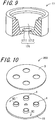
- the frame member 17 is disposed on the base 15, surrounding the sub-mount substrate 16. A detailed structure of the frame member 17 will be described, referring to Fig. 9 .
- a part of the frame member 17 is omitted from the drawing in order to show the internal structure of the frame member 17.
- the frame member 17 has a light reflecting portion 171 made of porous ceramics in which the plurality of ceramic particles 31 are partially integrated, and which has a plurality of pores, as illustrated in Fig. 3 .
- the porous ceramics has a porosity included in a range of 15% to 43%.
- the light reflecting portion 171 has a first surface 1711 and a second surface 1712.
- the first surface 1711 is horizontal.
- the second surface 1712 being disposed above the first surface 1711, is inclined.
- the light reflecting portion 171 scatters the light emitted from the light emitting diode 11, as illustrated in Fig. 2 . As the interfaces between the ceramic particles 31 and mediums 32 face in various directions, as illustrated in Fig. 3 , the light emitted from the light emitting diode 11 is scattered. The light emitted from the light emitting diode 11 is totally reflected at the interfaces between the ceramic particles 31 and the mediums 32.
- the light reflecting portion 171 is a total-reflection type optical section based on a difference in refractive indices. The light, due to total reflection, is unlikely to be lost.
- the light reflecting portion 171 corresponds to the second light reflecting portion 13 illustrated in Fig. 1 .
- the light emitting device 1 includes the sub-mount substrate 16, which has the upper surface 162 made of a ceramic sintered body, and the light reflecting portion 171 made of porous ceramics. With this kind of configuration, the bias of the light radiated downward from the light emitting diode 11 is reduced.
- the light emitting device 1 includes the base 15 made essentially of a metallic material, and the sub-mount substrate 16 made of a ceramic sintered body. Consequently, the light emitting device 1 is improved with respect to heat control.
- An illumination device 200 has a base 15 and a plurality of light emitting units 4.
- the illumination device 200 further has a cover 3 covering the base 15.
- the base 15 is made essentially of a metallic material.
- An example of the metallic material is copper (Cu).
- An insulating layer 18 is formed on the base 15.
- the insulating layer 18 is made essentially of a glass epoxy.
- a conductor pattern 19 is formed on the insulating layer 18.
- a resist layer 20 is formed on the conductor pattern 19.
- the plurality of light emitting units 4 are disposed on the common base 15. As illustrated in Fig. 11 , the plurality of light emitting units 4 have a plurality of light emitting diodes 11, a plurality of wavelength converting members 14, and a plurality of sub-mount substrates 16. The light emitting diode 11, wavelength converting member 14, and sub-mount substrate 16 have the same configurations illustrated in Fig. 7 . The plurality of light emitting units 4 further have a plurality of frame members 17. The frame member 17 has the same configuration illustrated in Fig. 7 .
- the illumination device 200 includes the sub-mount substrate 16, which has an upper surface 162 made of a ceramic sintered body, and a light reflecting portion 171 made of porous ceramics. With this kind of configuration, the bias of the light emitted downward from the light emitting diode 11 is reduced.
- the illumination device 200 is improved with respect to light emitting efficiency.
- the illumination device 200 includes the base 15 made essentially of a metallic material, and the sub-mount substrate 16 made of a ceramic sintered body. Consequently, the light emitting device 1 is improved with respect to heat control.
- the plurality of light emitting units 4 are disposed on the common base 15 made essentially of a metallic material. Consequently, the illumination device 200 is improved with respect to heat control.
Landscapes
- Led Device Packages (AREA)
Description
- The present invention relates to a light emitting device comprising a light emitting diode and an illumination device comprising such a light emitting device.
- In recent years, the development of a light emitting device comprising a light emitting diode is progressing in the field of illumination, and the like. This light emitting device has a wavelength converting member that converts the wavelength of a light emitted by the light emitting diode. Hereinafter, a further improvement in light emitting efficiency in the light emitting device is required.
-
EP 1496551 A1 discloses a light emitting device in which a light emitting diode is mounted on a submount that is surrounded by a plate section and mounted on a metallic part. The submount and plate section are made of a porous ceramic with a porosity of 5-20%. The arrangement is covered by a wavelength converting member. -
US 2007/0058357 A1 discloses a lighting device in which a substrate carries a light emitting diode. The substrate is mounted in a recess of a body part. -
US 2007/0235746 A1 discloses a light emitting device where a light emitting diode is placed on a submount disposed on a base and surrounded by a frame member with an inclined surface. The base, submount and frame member are made of a porous ceramic with a porosity of 10-50%. -
WO 2006/104061 A1 discloses a light emitting device having a base and a frame member that have a porous reflective layer with a porosity of 15-43% and that is made of inorganic material and having inorganic particles integrated. -
JP 2007227868 A - In order to improve the light emitting efficiency in the light emitting device, it is necessary to improve the efficiency of the wavelength conversion of the light emitted by the light emitting diode. Generally, there is a tendency for light radiated downward from the light emitting diode to arrive at a specific portion of the wavelength converting member with bias. In order to improve the efficiency of the wavelength conversion with the wavelength converting member, it is necessary to reduce the bias of the light radiated downward from the light emitting diode.
- The present invention provides a light emitting device as defined in
claim 1, and an illumination device as defined inclaim 4. Further embodiments of the present invention are described in the dependent claims. - Other and further objects, features, and advantages of the invention will be more explicit from the following detailed description taken with reference to the drawings wherein:
-
Fig. 1 illustrates a concept of the invention; -
Fig. 2 illustrates a light emitting structure of alight emitting device 1 illustrated inFig. 1 ; -
Fig. 3 illustrates an enlarged view of a portion indicated by reference numeral III ofFig. 2 ; -
Fig. 4 illustrates anillumination device 100 according to one embodiment of the invention; -
Fig. 5 illustrates asubstrate 2 ofFig. 4 ; -
Fig. 6 illustrates a vertical cross-section along VI-VI' ofFig. 4 ; -
Fig. 7 illustrates a cross-section of thelight emitting device 1 illustrated inFig. 6 ; -
Fig. 8 illustrates asub-mount substrate 16 illustrated inFig. 7 ; -
Fig. 9 illustrates aframe member 17 illustrated inFig. 7 ; -
Fig. 10 illustrates anillumination device 200 according to another embodiment of the invention; and -
Fig. 11 illustrates a vertical cross-section along XI-XI' ofFig. 10 . - Hereinafter, the concept of the invention will be described, referring to
Fig. 1 . Alight emitting device 1 includes alight emitting diode 11, a firstlight reflecting portion 12, and a secondlight reflecting portion 13. Thelight emitting device 1 further includes awavelength converting member 14. The light emitting diode emits a primary light. The firstlight reflecting portion 12 is disposed immediately below thelight emitting diode 11, and reflects the primary light. The secondlight reflecting portion 13 surrounds the firstlight reflecting portion 12, and reflects the primary light. The secondlight reflecting portion 13 scatters the primary light. Thewavelength converting member 14 emits a secondary light in dependence on the primary light. - A light emitting structure in the
light emitting device 1 will be described, referring toFig. 2 . The intensity of the primary light emitted from thelight emitting diode 11 diminishes as it is farther from thelight emitting diode 11. The firstlight reflecting portion 12 reflects relatively intense a primary light L11. The primary light L11 is specularly reflected. The secondlight reflecting portion 13 reflects relatively weak a primary light L12. The primary light L12 is scattered. Thewavelength converting member 14 emits a secondary light L2 in dependence on the primary light emitted from thelight emitting diode 11, including the lights L11 and L12 reflected by the firstlight reflecting portion 12 and secondlight reflecting portion 13. The exemplified secondary light L2 is white light. - Details of the portion indicated by reference numeral III in
Fig. 2 will be described, referring toFig. 3 . The secondlight reflecting portion 13 is made of a plurality ofinorganic particles 31 having a tranparence. The "transparence" of theinorganic particles 31 means that at least a part of wavelengths of the light emitted from thelight emitting diode 11 is transmitted. The secondlight reflecting portion 13 has a plurality ofmediums 32 of a smaller refractive index than that of theinorganic particles 31. Examples of themediums 32 are air, a resin material, or a glass material. The light L12 is transmitted through theinorganic particles 31. The light L12 is totally reflected at the interfaces between theinorganic particles 31 and themediums 32. In this way, the secondlight reflecting portion 13 is a total-reflection type optical section based on a difference in refractive indices. The light L12, due to total reflection, is unlikely to be lost. As the interfaces between theinorganic particles 31 and themediums 32 face in various directions, the light L12 is scattered. In thelight emitting device 1, a bias of the light emitted downward from thelight emitting diode 11 is reduced. - Consequently, the light emitting efficiency of the
light emitting device 1 is improved. - An
illumination device 100 according to one embodiment of the invention will be described, referring toFig. 4 . Theillumination device 100 has a plurality of light emittingdevices 1, asubstrate 2, and acover 3. Details of thesubstrate 2 will be described, referring toFig. 5 . Thesubstrate 2 has aconductor pattern 21 electrically connected to the plurality of light emittingdevices 1. Thesubstrate 2 has aprotective layer 22 formed on theconductor pattern 21. InFig. 5 , theprotective layer 22 is illustrated in a perspective view. A cross-sectional structure along VI-VI' ofFig. 4 will be described, referring toFig. 6 . The plurality of thelight emitting devices 1 are mounted on thesubstrate 2. The plurality of light emittingdevices 1 are electrically connected to theconductor pattern 21 bywires 4a. - A detailed structure of the
light emitting device 1 will be described, referring toFig. 7 . Thelight emitting device 1 has thelight emitting diode 11, thewavelength converting member 14, and abase 15. Thelight emitting device 1 further has asub-mount substrate 16 and aframe memebr 17. - The
light emitting diode 11 is mounted on thesub-mount substrate 16 by a flip-chip connection. Thelight emitting diode 11 is a light source which emits the primary light using drive power. The exemplified primary light has a wavelength included in the ultraviolet region. - The
wavelength converting member 14, covering thelight emitting diode 11, has a sheet shape. Thewavelength converting member 14 includes a base member having a transparence and a plurality of fluorescent particles. The "transparence" of the base member means that at least a part of wavelengths of the light emitted from thelight emitting diode 11 is transmitted. An example of the base member is a silicone resin. The plurality of fluorescent particles are dispersed inside the base member. Thewavelength converting member 14 emits the secondary light in dependence on the primary light. The exemplified secondary light is white light. - The exemplified
base 15 is made essentially of a metallic material. An example of the metallic material is copper (Cu). An insulatinglayer 18 is formed on thebase 15. The exemplified insulatinglayer 18 is made essentially of a glass epoxy. Aconductor pattern 19 is formed on the insulatinglayer 18, and is electrically connected to thelight emitting diode 11. A resistlayer 20 is formed on theconductor pattern 19. - The
sub-mount substrate 16 is disposed on thebase 15. Details of thesub-mount substrate 16 will be described, referring toFig. 8 . InFig. 8 , thelight emitting diode 11 is illustrated in a see-through manner in order to show the upper surface of thesub-mount substrate 16. Thesub-mount substrate 16 has aconductor pattern 161. Theconductor pattern 161 is electrically connected to thelight emitting diode 11. Thesub-mount substrate 16 has anupper surface 162 made of a ceramic sintered body having a porosity included in a range of 0.001% to 1%. An exemplified measurement method of the porosity is a mercury intrusion method using a Micromeritics Pore Sizer 9310. Theupper surface 162 corresponds to the firstlight reflecting portion 12 illustrated inFig. 1 . Thesub-mount substrate 16 is made entirely of a ceramic sintered body. - The
frame member 17 is disposed on thebase 15, surrounding thesub-mount substrate 16. A detailed structure of theframe member 17 will be described, referring toFig. 9 . InFig. 9 , a part of theframe member 17 is omitted from the drawing in order to show the internal structure of theframe member 17. Theframe member 17 has alight reflecting portion 171 made of porous ceramics in which the plurality ofceramic particles 31 are partially integrated, and which has a plurality of pores, as illustrated inFig. 3 . The porous ceramics has a porosity included in a range of 15% to 43%. Thelight reflecting portion 171 has afirst surface 1711 and asecond surface 1712. Thefirst surface 1711 is horizontal. Thesecond surface 1712, being disposed above thefirst surface 1711, is inclined. Thelight reflecting portion 171 scatters the light emitted from thelight emitting diode 11, as illustrated inFig. 2 . As the interfaces between theceramic particles 31 andmediums 32 face in various directions, as illustrated inFig. 3 , the light emitted from thelight emitting diode 11 is scattered. The light emitted from thelight emitting diode 11 is totally reflected at the interfaces between theceramic particles 31 and themediums 32. Thelight reflecting portion 171 is a total-reflection type optical section based on a difference in refractive indices. The light, due to total reflection, is unlikely to be lost. Thelight reflecting portion 171 corresponds to the secondlight reflecting portion 13 illustrated inFig. 1 . - The
light emitting device 1 includes thesub-mount substrate 16, which has theupper surface 162 made of a ceramic sintered body, and thelight reflecting portion 171 made of porous ceramics. With this kind of configuration, the bias of the light radiated downward from thelight emitting diode 11 is reduced. - Consequently, the light emitting efficiency of the
light emitting device 1 is improved. - The
light emitting device 1 includes the base 15 made essentially of a metallic material, and thesub-mount substrate 16 made of a ceramic sintered body. Consequently, thelight emitting device 1 is improved with respect to heat control. - Hereinafter, an illumination device according to another embodiment of the invention will be described, referring to
Fig. 10 . Anillumination device 200 has abase 15 and a plurality of light emittingunits 4. Theillumination device 200 further has acover 3 covering thebase 15. Thebase 15 is made essentially of a metallic material. An example of the metallic material is copper (Cu). An insulatinglayer 18 is formed on thebase 15. The insulatinglayer 18 is made essentially of a glass epoxy. Aconductor pattern 19 is formed on the insulatinglayer 18. A resistlayer 20 is formed on theconductor pattern 19. - The plurality of light emitting
units 4 are disposed on thecommon base 15. As illustrated inFig. 11 , the plurality of light emittingunits 4 have a plurality oflight emitting diodes 11, a plurality ofwavelength converting members 14, and a plurality ofsub-mount substrates 16. Thelight emitting diode 11,wavelength converting member 14, andsub-mount substrate 16 have the same configurations illustrated inFig. 7 . The plurality of light emittingunits 4 further have a plurality offrame members 17. Theframe member 17 has the same configuration illustrated inFig. 7 . - The
illumination device 200 includes thesub-mount substrate 16, which has anupper surface 162 made of a ceramic sintered body, and alight reflecting portion 171 made of porous ceramics. With this kind of configuration, the bias of the light emitted downward from thelight emitting diode 11 is reduced. - Consequently, the
illumination device 200 is improved with respect to light emitting efficiency. - The
illumination device 200 includes the base 15 made essentially of a metallic material, and thesub-mount substrate 16 made of a ceramic sintered body. Consequently, thelight emitting device 1 is improved with respect to heat control. - The plurality of light emitting
units 4 are disposed on thecommon base 15 made essentially of a metallic material. Consequently, theillumination device 200 is improved with respect to heat control. - The present embodiments are to be considered in all respects as illustrative and not restrictive, the scope of the invention being defined by the appended claims.
Claims (5)
- A light emitting device, comprising:a base (15);a sub-mount substrate (16) disposed on the base (15) and having an upper surface (12, 162) made of a ceramic sintered body having a porosity included in a range of 0.001% to 1%, the upper surface (12, 162) forming a light reflecting portion (12, 162);a frame member (17) disposed on the base (15), surrounding the sub-mount substrate (16) and having a light reflecting portion (13, 171) made of porous ceramics having a porosity included in a range of 15% to 43%;a light emitting diode (11) mounted on the light reflecting portion (12, 162) of the sub-mount substrate (16); anda wavelength converting member (14) covering the light emitting diode (11), the light reflecting portion (12, 162) of the sub-mount substrate (16), and the light reflecting portion (13, 171) of the frame member (17),wherein the light reflecting portion (13, 171) of the frame member (17) has a first surface (1711) and a second surface (1712) disposed above the first surface (1711), wherein the first surface (1711) is horizontal and the second surface (1712) is inclined, and wherein the light reflecting portion (13, 171) of the frame member (17) scatters light emitted from the light emitting diode (11).
- The light emitting device according to claim 1, wherein the wavelength converting member (14) has a sheet shape.
- The light emitting device according to claim 1, wherein the sub-mount substrate (16) is made entirely of a ceramic sintered body.
- An illumination device, comprising:a plurality of light emitting devices according to one of the preceding claims, whereinsaid base (15) includes a metallic material;a plurality of said sub-mount substrates (16) are disposed on the base (15) and each has an upper surface made of a ceramic sintered body;a plurality of frame members (17) are disposed on the base (15), each surrounding one of the sub-mount substrates (16) and each having a light reflecting portion (13, 171) made of porous ceramics;a plurality of said light emitting diodes (11) are mounted on a respective one of the plurality of sub-mount substrates (16); anda plurality of wavelength converting members (14) are provided, each covering one of the light emitting diodes (11) and one of the light reflecting portions (13, 171).
- The illumination device according to claim 4, comprising:a substrate (2) having a conductor pattern (21);a plurality of bases (15) including a metallic material;wherein the light emitting diodes (11) are electrically connected to the conductor pattern (21).
Applications Claiming Priority (2)
| Application Number | Priority Date | Filing Date | Title |
|---|---|---|---|
| JP2007333621 | 2007-12-26 | ||
| PCT/JP2008/073858 WO2009082011A1 (en) | 2007-12-26 | 2008-12-26 | Light-emitting device and illuminating device |
Publications (3)
| Publication Number | Publication Date |
|---|---|
| EP2237331A1 EP2237331A1 (en) | 2010-10-06 |
| EP2237331A4 EP2237331A4 (en) | 2013-05-01 |
| EP2237331B1 true EP2237331B1 (en) | 2017-01-25 |
Family
ID=40801308
Family Applications (1)
| Application Number | Title | Priority Date | Filing Date |
|---|---|---|---|
| EP08863988.5A Not-in-force EP2237331B1 (en) | 2007-12-26 | 2008-12-26 | Light-emitting device and illuminating device |
Country Status (5)
| Country | Link |
|---|---|
| US (1) | US8529089B2 (en) |
| EP (1) | EP2237331B1 (en) |
| JP (1) | JP5259627B2 (en) |
| TW (1) | TW200946833A (en) |
| WO (1) | WO2009082011A1 (en) |
Cited By (1)
| Publication number | Priority date | Publication date | Assignee | Title |
|---|---|---|---|---|
| EP3869638B1 (en) * | 2017-03-03 | 2024-06-19 | Nichia Corporation | Optical component |
Families Citing this family (12)
| Publication number | Priority date | Publication date | Assignee | Title |
|---|---|---|---|---|
| EP2495774B1 (en) * | 2009-10-29 | 2018-07-18 | Kyocera Corporation | Light emitting device |
| JP2013065706A (en) * | 2011-09-16 | 2013-04-11 | Sumitomo Bakelite Co Ltd | Heat generation device assembly and manufacturing method of the same |
| JP5533827B2 (en) * | 2011-09-20 | 2014-06-25 | 豊田合成株式会社 | Linear light source device |
| CN103968332B (en) | 2013-01-25 | 2015-10-07 | 深圳市光峰光电技术有限公司 | A kind of Wavelength converter, light-emitting device and optical projection system |
| DE102013207111B4 (en) * | 2013-04-19 | 2021-07-01 | OSRAM Opto Semiconductors Gesellschaft mit beschränkter Haftung | Optoelectronic component |
| KR20150093283A (en) * | 2014-02-06 | 2015-08-18 | 삼성디스플레이 주식회사 | Frame and light source module comprising the same |
| KR102166715B1 (en) * | 2014-04-02 | 2020-10-19 | 삼성디스플레이 주식회사 | Light source unit, and method for manufacturing the same, and backlight assembly including the same |
| CN108901197B (en) * | 2016-03-24 | 2022-04-22 | 索尼公司 | Light emitting device, display apparatus, and illumination apparatus |
| CN109791968A (en) * | 2016-07-26 | 2019-05-21 | 克利公司 | Light emitting diode, component and correlation technique |
| US11024785B2 (en) | 2018-05-25 | 2021-06-01 | Creeled, Inc. | Light-emitting diode packages |
| EP3820132B1 (en) * | 2018-07-05 | 2023-08-23 | Mitsubishi Electric Corporation | Lighting device and image reading device |
| DE102018132542A1 (en) * | 2018-12-17 | 2020-06-18 | Osram Opto Semiconductors Gmbh | OPTOELECTRONIC LIGHTING DEVICE AND MANUFACTURING METHOD |
Family Cites Families (19)
| Publication number | Priority date | Publication date | Assignee | Title |
|---|---|---|---|---|
| JPS6054175U (en) * | 1983-09-19 | 1985-04-16 | 三洋電機株式会社 | light emitting diode display |
| JP2787953B2 (en) * | 1989-08-03 | 1998-08-20 | イビデン株式会社 | Electronic circuit board |
| JP4045781B2 (en) * | 2001-08-28 | 2008-02-13 | 松下電工株式会社 | Light emitting device |
| US7495322B2 (en) * | 2003-05-26 | 2009-02-24 | Panasonic Electric Works Co., Ltd. | Light-emitting device |
| US7211835B2 (en) * | 2003-07-09 | 2007-05-01 | Nichia Corporation | Light emitting device, method of manufacturing the same and lighting equipment |
| US20050133808A1 (en) * | 2003-09-11 | 2005-06-23 | Kyocera Corporation | Package for housing light-emitting element, light-emitting apparatus and illumination apparatus |
| JP4206334B2 (en) | 2003-12-25 | 2009-01-07 | 京セラ株式会社 | Light emitting device |
| EP1686630A3 (en) | 2005-01-31 | 2009-03-04 | Samsung Electronics Co., Ltd. | Led device having diffuse reflective surface |
| EP1873563B1 (en) | 2005-03-29 | 2017-03-22 | Kyocera Corporation | Light-emitting device using reflective member and illuminating device |
| JP4773755B2 (en) * | 2005-07-01 | 2011-09-14 | ローム株式会社 | Chip-type semiconductor light emitting device |
| JP3998027B2 (en) | 2005-07-25 | 2007-10-24 | 松下電工株式会社 | Lighting equipment using LED |
| JP2007081234A (en) * | 2005-09-15 | 2007-03-29 | Toyoda Gosei Co Ltd | Lighting device |
| JP2007142051A (en) * | 2005-11-16 | 2007-06-07 | Matsushita Electric Ind Co Ltd | Light emitting module |
| CN101846247B (en) * | 2005-12-22 | 2013-04-17 | 松下电器产业株式会社 | Lighting apparatus with LED |
| JP4926481B2 (en) * | 2006-01-26 | 2012-05-09 | 共立エレックス株式会社 | Light emitting diode package and light emitting diode |
| JP4744335B2 (en) * | 2006-01-30 | 2011-08-10 | 京セラ株式会社 | Light emitting device and lighting device |
| JP4688695B2 (en) * | 2006-02-24 | 2011-05-25 | 京セラ株式会社 | LIGHT REFLECTOR, LIGHT EMITTING ELEMENT WIRING BOARD, AND LIGHT EMITTING DEVICE |
| JP2007305844A (en) * | 2006-05-12 | 2007-11-22 | Stanley Electric Co Ltd | Light emitting device and manufacturing method thereof |
| US20080112165A1 (en) * | 2006-11-15 | 2008-05-15 | Kyocera Corporation | Light-emitting device |
-
2008
- 2008-12-26 JP JP2009547148A patent/JP5259627B2/en not_active Expired - Fee Related
- 2008-12-26 US US12/810,769 patent/US8529089B2/en not_active Expired - Fee Related
- 2008-12-26 WO PCT/JP2008/073858 patent/WO2009082011A1/en not_active Ceased
- 2008-12-26 TW TW097151292A patent/TW200946833A/en unknown
- 2008-12-26 EP EP08863988.5A patent/EP2237331B1/en not_active Not-in-force
Non-Patent Citations (1)
| Title |
|---|
| None * |
Cited By (1)
| Publication number | Priority date | Publication date | Assignee | Title |
|---|---|---|---|---|
| EP3869638B1 (en) * | 2017-03-03 | 2024-06-19 | Nichia Corporation | Optical component |
Also Published As
| Publication number | Publication date |
|---|---|
| JP5259627B2 (en) | 2013-08-07 |
| TW200946833A (en) | 2009-11-16 |
| EP2237331A1 (en) | 2010-10-06 |
| US8529089B2 (en) | 2013-09-10 |
| US20110096526A1 (en) | 2011-04-28 |
| EP2237331A4 (en) | 2013-05-01 |
| WO2009082011A1 (en) | 2009-07-02 |
| JPWO2009082011A1 (en) | 2011-05-06 |
Similar Documents
| Publication | Publication Date | Title |
|---|---|---|
| US8529089B2 (en) | Light emitting device and illumination device | |
| KR101816669B1 (en) | Illumination apparatus | |
| EP3025380B1 (en) | Flip-chip side emitting led | |
| CN101410993B (en) | Light emitting device | |
| EP3095142B1 (en) | Led module with uniform phosphor illumination | |
| WO2008103379A1 (en) | Led lighting systems including luminescent layers on remote reflectors | |
| US20130009183A1 (en) | Reflective circuit board for led backlight | |
| US20100259916A1 (en) | Light-emitting device and method for fabricating the same | |
| JP5014182B2 (en) | Light emitting device | |
| KR101646262B1 (en) | Light emitting device package and light unit having the seme | |
| JP4948818B2 (en) | Light emitting device and lighting device | |
| EP2237330B1 (en) | Light emitting device | |
| JP5451091B2 (en) | Light emitting device and lighting device | |
| JP2009158634A (en) | Light emitting device | |
| JP2009289509A (en) | Illuminating device | |
| JP2010129711A (en) | Light-emitting device | |
| KR20160059709A (en) | Light Emitting Module | |
| JP2017228712A (en) | LED light emitting device | |
| JP2010129712A (en) | Light-emitting device | |
| KR101315702B1 (en) | Lighting module | |
| WO2011024502A1 (en) | Light emitting device | |
| JP2010153595A (en) | Light-emitting device | |
| JP2009158635A (en) | Light emitting device |
Legal Events
| Date | Code | Title | Description |
|---|---|---|---|
| PUAI | Public reference made under article 153(3) epc to a published international application that has entered the european phase |
Free format text: ORIGINAL CODE: 0009012 |
|
| 17P | Request for examination filed |
Effective date: 20100726 |
|
| AK | Designated contracting states |
Kind code of ref document: A1 Designated state(s): AT BE BG CH CY CZ DE DK EE ES FI FR GB GR HR HU IE IS IT LI LT LU LV MC MT NL NO PL PT RO SE SI SK TR |
|
| AX | Request for extension of the european patent |
Extension state: AL BA MK RS |
|
| DAX | Request for extension of the european patent (deleted) | ||
| A4 | Supplementary search report drawn up and despatched |
Effective date: 20130328 |
|
| RIC1 | Information provided on ipc code assigned before grant |
Ipc: F21K 99/00 20100101AFI20130322BHEP Ipc: H01L 33/60 20100101ALN20130322BHEP Ipc: H01L 33/50 20100101ALN20130322BHEP Ipc: F21Y 101/02 20060101ALN20130322BHEP |
|
| 17Q | First examination report despatched |
Effective date: 20160502 |
|
| REG | Reference to a national code |
Ref country code: DE Ref legal event code: R079 Ref document number: 602008048618 Country of ref document: DE Free format text: PREVIOUS MAIN CLASS: H01L0033000000 Ipc: H01L0033480000 |
|
| GRAP | Despatch of communication of intention to grant a patent |
Free format text: ORIGINAL CODE: EPIDOSNIGR1 |
|
| INTG | Intention to grant announced |
Effective date: 20160720 |
|
| RIC1 | Information provided on ipc code assigned before grant |
Ipc: H01L 33/50 20100101ALN20160708BHEP Ipc: H01L 33/60 20100101ALI20160708BHEP Ipc: H01L 33/48 20100101AFI20160708BHEP Ipc: F21K 9/60 20160101ALI20160708BHEP |
|
| STAA | Information on the status of an ep patent application or granted ep patent |
Free format text: STATUS: GRANT OF PATENT IS INTENDED |
|
| GRAS | Grant fee paid |
Free format text: ORIGINAL CODE: EPIDOSNIGR3 |
|
| GRAA | (expected) grant |
Free format text: ORIGINAL CODE: 0009210 |
|
| STAA | Information on the status of an ep patent application or granted ep patent |
Free format text: STATUS: THE PATENT HAS BEEN GRANTED |
|
| AK | Designated contracting states |
Kind code of ref document: B1 Designated state(s): AT BE BG CH CY CZ DE DK EE ES FI FR GB GR HR HU IE IS IT LI LT LU LV MC MT NL NO PL PT RO SE SI SK TR |
|
| REG | Reference to a national code |
Ref country code: GB Ref legal event code: FG4D |
|
| REG | Reference to a national code |
Ref country code: CH Ref legal event code: EP |
|
| REG | Reference to a national code |
Ref country code: AT Ref legal event code: REF Ref document number: 864576 Country of ref document: AT Kind code of ref document: T Effective date: 20170215 |
|
| REG | Reference to a national code |
Ref country code: IE Ref legal event code: FG4D |
|
| REG | Reference to a national code |
Ref country code: DE Ref legal event code: R096 Ref document number: 602008048618 Country of ref document: DE |
|
| REG | Reference to a national code |
Ref country code: LT Ref legal event code: MG4D |
|
| REG | Reference to a national code |
Ref country code: NL Ref legal event code: MP Effective date: 20170125 |
|
| REG | Reference to a national code |
Ref country code: AT Ref legal event code: MK05 Ref document number: 864576 Country of ref document: AT Kind code of ref document: T Effective date: 20170125 |
|
| PG25 | Lapsed in a contracting state [announced via postgrant information from national office to epo] |
Ref country code: NL Free format text: LAPSE BECAUSE OF FAILURE TO SUBMIT A TRANSLATION OF THE DESCRIPTION OR TO PAY THE FEE WITHIN THE PRESCRIBED TIME-LIMIT Effective date: 20170125 |
|
| PG25 | Lapsed in a contracting state [announced via postgrant information from national office to epo] |
Ref country code: FI Free format text: LAPSE BECAUSE OF FAILURE TO SUBMIT A TRANSLATION OF THE DESCRIPTION OR TO PAY THE FEE WITHIN THE PRESCRIBED TIME-LIMIT Effective date: 20170125 Ref country code: NO Free format text: LAPSE BECAUSE OF FAILURE TO SUBMIT A TRANSLATION OF THE DESCRIPTION OR TO PAY THE FEE WITHIN THE PRESCRIBED TIME-LIMIT Effective date: 20170425 Ref country code: HR Free format text: LAPSE BECAUSE OF FAILURE TO SUBMIT A TRANSLATION OF THE DESCRIPTION OR TO PAY THE FEE WITHIN THE PRESCRIBED TIME-LIMIT Effective date: 20170125 Ref country code: LT Free format text: LAPSE BECAUSE OF FAILURE TO SUBMIT A TRANSLATION OF THE DESCRIPTION OR TO PAY THE FEE WITHIN THE PRESCRIBED TIME-LIMIT Effective date: 20170125 Ref country code: GR Free format text: LAPSE BECAUSE OF FAILURE TO SUBMIT A TRANSLATION OF THE DESCRIPTION OR TO PAY THE FEE WITHIN THE PRESCRIBED TIME-LIMIT Effective date: 20170426 Ref country code: IS Free format text: LAPSE BECAUSE OF FAILURE TO SUBMIT A TRANSLATION OF THE DESCRIPTION OR TO PAY THE FEE WITHIN THE PRESCRIBED TIME-LIMIT Effective date: 20170525 |
|
| PG25 | Lapsed in a contracting state [announced via postgrant information from national office to epo] |
Ref country code: PT Free format text: LAPSE BECAUSE OF FAILURE TO SUBMIT A TRANSLATION OF THE DESCRIPTION OR TO PAY THE FEE WITHIN THE PRESCRIBED TIME-LIMIT Effective date: 20170525 Ref country code: ES Free format text: LAPSE BECAUSE OF FAILURE TO SUBMIT A TRANSLATION OF THE DESCRIPTION OR TO PAY THE FEE WITHIN THE PRESCRIBED TIME-LIMIT Effective date: 20170125 Ref country code: SE Free format text: LAPSE BECAUSE OF FAILURE TO SUBMIT A TRANSLATION OF THE DESCRIPTION OR TO PAY THE FEE WITHIN THE PRESCRIBED TIME-LIMIT Effective date: 20170125 Ref country code: PL Free format text: LAPSE BECAUSE OF FAILURE TO SUBMIT A TRANSLATION OF THE DESCRIPTION OR TO PAY THE FEE WITHIN THE PRESCRIBED TIME-LIMIT Effective date: 20170125 Ref country code: BG Free format text: LAPSE BECAUSE OF FAILURE TO SUBMIT A TRANSLATION OF THE DESCRIPTION OR TO PAY THE FEE WITHIN THE PRESCRIBED TIME-LIMIT Effective date: 20170425 Ref country code: AT Free format text: LAPSE BECAUSE OF FAILURE TO SUBMIT A TRANSLATION OF THE DESCRIPTION OR TO PAY THE FEE WITHIN THE PRESCRIBED TIME-LIMIT Effective date: 20170125 Ref country code: LV Free format text: LAPSE BECAUSE OF FAILURE TO SUBMIT A TRANSLATION OF THE DESCRIPTION OR TO PAY THE FEE WITHIN THE PRESCRIBED TIME-LIMIT Effective date: 20170125 |
|
| REG | Reference to a national code |
Ref country code: DE Ref legal event code: R097 Ref document number: 602008048618 Country of ref document: DE |
|
| PG25 | Lapsed in a contracting state [announced via postgrant information from national office to epo] |
Ref country code: CZ Free format text: LAPSE BECAUSE OF FAILURE TO SUBMIT A TRANSLATION OF THE DESCRIPTION OR TO PAY THE FEE WITHIN THE PRESCRIBED TIME-LIMIT Effective date: 20170125 Ref country code: EE Free format text: LAPSE BECAUSE OF FAILURE TO SUBMIT A TRANSLATION OF THE DESCRIPTION OR TO PAY THE FEE WITHIN THE PRESCRIBED TIME-LIMIT Effective date: 20170125 Ref country code: RO Free format text: LAPSE BECAUSE OF FAILURE TO SUBMIT A TRANSLATION OF THE DESCRIPTION OR TO PAY THE FEE WITHIN THE PRESCRIBED TIME-LIMIT Effective date: 20170125 Ref country code: SK Free format text: LAPSE BECAUSE OF FAILURE TO SUBMIT A TRANSLATION OF THE DESCRIPTION OR TO PAY THE FEE WITHIN THE PRESCRIBED TIME-LIMIT Effective date: 20170125 Ref country code: IT Free format text: LAPSE BECAUSE OF FAILURE TO SUBMIT A TRANSLATION OF THE DESCRIPTION OR TO PAY THE FEE WITHIN THE PRESCRIBED TIME-LIMIT Effective date: 20170125 |
|
| PG25 | Lapsed in a contracting state [announced via postgrant information from national office to epo] |
Ref country code: DK Free format text: LAPSE BECAUSE OF FAILURE TO SUBMIT A TRANSLATION OF THE DESCRIPTION OR TO PAY THE FEE WITHIN THE PRESCRIBED TIME-LIMIT Effective date: 20170125 |
|
| PLBE | No opposition filed within time limit |
Free format text: ORIGINAL CODE: 0009261 |
|
| STAA | Information on the status of an ep patent application or granted ep patent |
Free format text: STATUS: NO OPPOSITION FILED WITHIN TIME LIMIT |
|
| 26N | No opposition filed |
Effective date: 20171026 |
|
| PG25 | Lapsed in a contracting state [announced via postgrant information from national office to epo] |
Ref country code: SI Free format text: LAPSE BECAUSE OF FAILURE TO SUBMIT A TRANSLATION OF THE DESCRIPTION OR TO PAY THE FEE WITHIN THE PRESCRIBED TIME-LIMIT Effective date: 20170125 |
|
| REG | Reference to a national code |
Ref country code: DE Ref legal event code: R119 Ref document number: 602008048618 Country of ref document: DE |
|
| REG | Reference to a national code |
Ref country code: CH Ref legal event code: PL |
|
| GBPC | Gb: european patent ceased through non-payment of renewal fee |
Effective date: 20171226 |
|
| REG | Reference to a national code |
Ref country code: IE Ref legal event code: MM4A |
|
| PG25 | Lapsed in a contracting state [announced via postgrant information from national office to epo] |
Ref country code: MT Free format text: LAPSE BECAUSE OF NON-PAYMENT OF DUE FEES Effective date: 20171226 Ref country code: LU Free format text: LAPSE BECAUSE OF NON-PAYMENT OF DUE FEES Effective date: 20171226 |
|
| REG | Reference to a national code |
Ref country code: FR Ref legal event code: ST Effective date: 20180831 |
|
| REG | Reference to a national code |
Ref country code: BE Ref legal event code: MM Effective date: 20171231 |
|
| PG25 | Lapsed in a contracting state [announced via postgrant information from national office to epo] |
Ref country code: DE Free format text: LAPSE BECAUSE OF NON-PAYMENT OF DUE FEES Effective date: 20180703 Ref country code: FR Free format text: LAPSE BECAUSE OF NON-PAYMENT OF DUE FEES Effective date: 20180102 Ref country code: IE Free format text: LAPSE BECAUSE OF NON-PAYMENT OF DUE FEES Effective date: 20171226 |
|
| PG25 | Lapsed in a contracting state [announced via postgrant information from national office to epo] |
Ref country code: LI Free format text: LAPSE BECAUSE OF NON-PAYMENT OF DUE FEES Effective date: 20171231 Ref country code: GB Free format text: LAPSE BECAUSE OF NON-PAYMENT OF DUE FEES Effective date: 20171226 Ref country code: CH Free format text: LAPSE BECAUSE OF NON-PAYMENT OF DUE FEES Effective date: 20171231 Ref country code: BE Free format text: LAPSE BECAUSE OF NON-PAYMENT OF DUE FEES Effective date: 20171231 |
|
| PG25 | Lapsed in a contracting state [announced via postgrant information from national office to epo] |
Ref country code: HU Free format text: LAPSE BECAUSE OF FAILURE TO SUBMIT A TRANSLATION OF THE DESCRIPTION OR TO PAY THE FEE WITHIN THE PRESCRIBED TIME-LIMIT; INVALID AB INITIO Effective date: 20081226 Ref country code: MC Free format text: LAPSE BECAUSE OF FAILURE TO SUBMIT A TRANSLATION OF THE DESCRIPTION OR TO PAY THE FEE WITHIN THE PRESCRIBED TIME-LIMIT Effective date: 20170125 |
|
| PG25 | Lapsed in a contracting state [announced via postgrant information from national office to epo] |
Ref country code: CY Free format text: LAPSE BECAUSE OF NON-PAYMENT OF DUE FEES Effective date: 20170125 |
|
| PG25 | Lapsed in a contracting state [announced via postgrant information from national office to epo] |
Ref country code: TR Free format text: LAPSE BECAUSE OF FAILURE TO SUBMIT A TRANSLATION OF THE DESCRIPTION OR TO PAY THE FEE WITHIN THE PRESCRIBED TIME-LIMIT Effective date: 20170125 |