EP2235794B1 - Press-in contact having base, contact pin and second pin - Google Patents
Press-in contact having base, contact pin and second pin Download PDFInfo
- Publication number
- EP2235794B1 EP2235794B1 EP08871024A EP08871024A EP2235794B1 EP 2235794 B1 EP2235794 B1 EP 2235794B1 EP 08871024 A EP08871024 A EP 08871024A EP 08871024 A EP08871024 A EP 08871024A EP 2235794 B1 EP2235794 B1 EP 2235794B1
- Authority
- EP
- European Patent Office
- Prior art keywords
- pin
- contact
- contact pin
- press
- tip
- Prior art date
- Legal status (The legal status is an assumption and is not a legal conclusion. Google has not performed a legal analysis and makes no representation as to the accuracy of the status listed.)
- Active
Links
- 238000000034 method Methods 0.000 claims description 24
- 238000003825 pressing Methods 0.000 description 14
- 230000002093 peripheral effect Effects 0.000 description 8
- RYGMFSIKBFXOCR-UHFFFAOYSA-N Copper Chemical compound [Cu] RYGMFSIKBFXOCR-UHFFFAOYSA-N 0.000 description 5
- 229910052802 copper Inorganic materials 0.000 description 5
- 239000010949 copper Substances 0.000 description 5
- 238000003780 insertion Methods 0.000 description 5
- 230000037431 insertion Effects 0.000 description 5
- 208000029154 Narrow face Diseases 0.000 description 3
- 238000006073 displacement reaction Methods 0.000 description 3
- 238000004519 manufacturing process Methods 0.000 description 2
- NJPPVKZQTLUDBO-UHFFFAOYSA-N novaluron Chemical compound C1=C(Cl)C(OC(F)(F)C(OC(F)(F)F)F)=CC=C1NC(=O)NC(=O)C1=C(F)C=CC=C1F NJPPVKZQTLUDBO-UHFFFAOYSA-N 0.000 description 2
- 239000004593 Epoxy Substances 0.000 description 1
- 238000005299 abrasion Methods 0.000 description 1
- 230000015572 biosynthetic process Effects 0.000 description 1
- 230000008021 deposition Effects 0.000 description 1
- 238000004049 embossing Methods 0.000 description 1
- 239000003365 glass fiber Substances 0.000 description 1
- 239000000463 material Substances 0.000 description 1
- 239000002184 metal Substances 0.000 description 1
- 229910052751 metal Inorganic materials 0.000 description 1
- 239000013528 metallic particle Substances 0.000 description 1
- 238000004080 punching Methods 0.000 description 1
- 238000003892 spreading Methods 0.000 description 1
- 238000003860 storage Methods 0.000 description 1
- 230000007704 transition Effects 0.000 description 1
Images


Classifications
-
- H—ELECTRICITY
- H01—ELECTRIC ELEMENTS
- H01R—ELECTRICALLY-CONDUCTIVE CONNECTIONS; STRUCTURAL ASSOCIATIONS OF A PLURALITY OF MUTUALLY-INSULATED ELECTRICAL CONNECTING ELEMENTS; COUPLING DEVICES; CURRENT COLLECTORS
- H01R12/00—Structural associations of a plurality of mutually-insulated electrical connecting elements, specially adapted for printed circuits, e.g. printed circuit boards [PCB], flat or ribbon cables, or like generally planar structures, e.g. terminal strips, terminal blocks; Coupling devices specially adapted for printed circuits, flat or ribbon cables, or like generally planar structures; Terminals specially adapted for contact with, or insertion into, printed circuits, flat or ribbon cables, or like generally planar structures
- H01R12/50—Fixed connections
- H01R12/51—Fixed connections for rigid printed circuits or like structures
- H01R12/55—Fixed connections for rigid printed circuits or like structures characterised by the terminals
- H01R12/58—Fixed connections for rigid printed circuits or like structures characterised by the terminals terminals for insertion into holes
- H01R12/585—Terminals having a press fit or a compliant portion and a shank passing through a hole in the printed circuit board
-
- Y—GENERAL TAGGING OF NEW TECHNOLOGICAL DEVELOPMENTS; GENERAL TAGGING OF CROSS-SECTIONAL TECHNOLOGIES SPANNING OVER SEVERAL SECTIONS OF THE IPC; TECHNICAL SUBJECTS COVERED BY FORMER USPC CROSS-REFERENCE ART COLLECTIONS [XRACs] AND DIGESTS
- Y10—TECHNICAL SUBJECTS COVERED BY FORMER USPC
- Y10T—TECHNICAL SUBJECTS COVERED BY FORMER US CLASSIFICATION
- Y10T29/00—Metal working
- Y10T29/49—Method of mechanical manufacture
- Y10T29/49002—Electrical device making
- Y10T29/49117—Conductor or circuit manufacturing
- Y10T29/49124—On flat or curved insulated base, e.g., printed circuit, etc.
- Y10T29/49128—Assembling formed circuit to base
Landscapes
- Coupling Device And Connection With Printed Circuit (AREA)
- Multi-Conductor Connections (AREA)
Abstract
Description
Die Erfindung betrifft einen Einpresskontakt mit einem Sockel, einem Kontaktstift und einem zweiten Stift, der sich parallel zu dem Kontaktstift erstreckt, ein Gehäuse mit einem Kontaktstift und einem zweiten Stift oder zwei weiteren Stiften, die sich parallel zu dem Kontaktstift erstrecken, ein Verfahren zum Einlegen einer Leiterplatte in ein Gehäuse mit einem Kontaktstift und einem zweiten Stift, der sich parallel zu dem Kontaktstift erstreckt sowie eine Leiterplatte mit zumindest zwei Ausnehmungen von den zumindest eine erste Ausnehmung eine Kontakthülse zur Aufnahme eines Einpresspins aufweist.The invention relates to a press-in contact with a socket, a contact pin and a second pin which extends parallel to the contact pin, a housing with a contact pin and a second pin or two further pins which extend parallel to the contact pin, a method for insertion a printed circuit board in a housing having a contact pin and a second pin which extends parallel to the contact pin and a printed circuit board having at least two recesses of the at least one first recess has a contact sleeve for receiving a Einpresspins.
Aus der
Aus der
Die Kontaktstifte weisen eine durch einen Stanz- und Prägeprozess geformte scharfkantige Pinspitze auf. In der Automobiltechnik werden Kunststoffgehäuse verwendet, in die diese Einpresskontakte als Einlegeteile einspritzbar sind. Eine Leiterplatte ist in das Kunststoffgehäuse einsetzbar und weist Ausnehmungen mit Kupferhülsen auf, um einen elektrisch leitfähigen Kontakt mit den Einpresspins der Einpresskontakte herzustellen. Während des Einsetzens der Leiterplatte in das Gehäuse durchstoßen die im Gehäuseinneren angeordneten Einpresspins die Kupferhülsen. Sind die Leiterplatte und das Gehäuse bei dem Einpressvorgang ungenau zueinander positioniert, so treten Beschädigungen an der Kupferhülse auf. Abgespante metallische Partikel verursachen elektrische Kurzschlüsse auf der Leiterplatte.The contact pins have a sharp-edged pin tip formed by a stamping and stamping process. In the automotive industry Plastic housing used, in which these press-fit contacts are injected as inserts. A circuit board is insertable into the plastic housing and has recesses with copper sleeves to make electrically conductive contact with the press-fit pins of the press-fit contacts. During insertion of the printed circuit board into the housing, the press-fit pins arranged inside the housing penetrate the copper sleeves. If the printed circuit board and the housing are positioned inaccurately relative to one another during the press-fitting process, damage to the copper sleeve occurs. Spilled metallic particles cause electrical short circuits on the circuit board.
Der Erfindung liegt die Aufgabe zugrunde, einen einfachen Einpresskontakt anzugeben. Insbesondere soll ein Hilfsmittel angegeben werden, mittels dessen eine einfache und genaue Positionierung zwischen Leiterplatte und eines in einem Gehäuse angeordneten Kontaktstiftes ermöglicht ist.The invention has for its object to provide a simple press-fit. In particular, an aid should be provided by means of which a simple and accurate positioning between the printed circuit board and a contact pin arranged in a housing is made possible.
Diese Aufgabe wird mit den Merkmalen der Hauptansprüche gelöst. Erfindungsgemäß ragt der zweite Stift über den Kontaktstift hinaus und weist in gleicher Höhe zu einer Spitze des Kontaktstiftes einen größten Umfang auf und ragen die zwei weiteren Stifte über den Kontaktstift hinaus und weisen in gleicher Höhe zu einer Spitze des Kontaktstiftes einen größten Umfang auf. Folgende Verfahrensschritte sind dabei angewandt: Die Leiterplatte wird von dem zweiten Stift in lateraler Richtung verschiebbar in das Gehäuse so eingesetzt, dass eine Spitze des Kontaktstiftes berührungsfrei in eine Ausnehmung eindringt und ein Einpressteil des Kontaktstiftes in die Leiterplatte eingepresst wird. Der zweite Stift fungiert als Vorzentrierpin und ist in seiner Länge etwas länger als der Kontaktstift und hat im Bereich der Pinspitze des Kontaktstiftes seine breiteste Stelle. Der Vorzentrierpin wird auch als Zentrierstift oder -pin bezeichnet. Die Breite des Vorzentrierpins an der breitesten Stelle ist so gewählt, dass die Toleranzen der Leiterplatte durch die spitz zulaufende Form der Vorzentrierspitze abgefangen werden, und die Leiterplatte beim Ablegen durch die Vorzentrierspitze lateral korrigiert wird. Der Einpresskontakt mit dem Kontaktstift und dem Vorzentrierpin wird in einem einzigen Prozessschritt hergestellt. Das Herstellungsverfahren ist ein Stanz-Prägeverfahren. Da der Kontaktstift und der Vorzentrierpin mit dem Sockel einteilig ausgebildet sind, sind Toleranzen geringfügig. Der Einpresskontakt ist mit geringen Toleranzen reproduzierbar.This object is achieved with the features of the main claims. According to the invention, the second pin protrudes beyond the contact pin and at the same height to a tip of the contact pin on a largest extent and protrude the two other pins beyond the contact pin and have at the same height to a tip of the contact pin on a largest circumference. The following method steps are used: The printed circuit board is slidably inserted into the housing from the second pin in a lateral direction such that a tip of the contact pin penetrates into a recess without contact and a press-fit part of the contact pin is pressed into the printed circuit board. The second pin acts as Vorzentrierpin and is slightly longer in its length than the contact pin and has its widest point in the area of the pin tip of the contact pin. The pre-centering pin is also referred to as a centering pin or pin. The width of the pre-centering pin at the widest point is chosen so that the tolerances of the circuit board are absorbed by the tapered shape of Vorzentrierspitze, and the circuit board is corrected laterally when dropped by the Vorzentrierspitze. The press-fit contact with the contact pin and the pre-centering pin is produced in a single process step. The manufacturing process is a stamping-stamping process. Since the contact pin and the Vorzentrierpin are integrally formed with the base, tolerances are small. The press-fit contact is reproducible with low tolerances.
In vorteilhafter Weise weist der Zentrierpin in Höhe und über eine Länge des Einpressteiles des Kontaktstiftes einen geringeren Umfang als das Einpressteil auf. Damit ist eine mechanische Überbestimmung der Leiterplatte im eingepressten Zustand sicher vermieden.In an advantageous manner, the centering pin has a smaller circumference than the press-in part at the level and over a length of the press-in part of the contact pin. For a mechanical over-determination of the circuit board in the pressed state is safely avoided.
In einfacher Weise ist der zweite Stift pfeilförmig mit einem quaderförmigen Schaft und einer Spitze ausgebildet. Nach der breitesten Stelle des Vorzentrierpins verjüngt sich der Vorzentrierpin in Richtung auf den Sockel und bildet den Schaft aus. Der Schaft ist länglich und von geringem Umfang. Damit ist die Leiterplatte nach dem Einpressvorgang lateral nicht überbestimmt. Die breiteste Stelle des Vorzentrierpins weist ein geringfügiges Spiel innerhalb der Vorzentrierbohrung auf, damit ist die Leiterplatte zu Beginn des Einpressvorgangs lateral nicht überbestimmt. Der Einpresskontakt ist auch als Einlegeteil bezeichnet, das in eine Form einlegbar und danach mit Kunststoff ummantelbar ist, also in ein Kunststoffgehäuse eingießbar ist. Die Lage der Leiterplatte innerhalb des Gehäuses ist lediglich durch die Einpresspins bestimmt. Aufgrund einer getrennten Herstellung des Einpresskontakts und des Gehäuses ist eine einfache Hinterschneidung des Zentrierpins ermöglicht.In a simple way, the second pin is formed in an arrow shape with a cuboid shaft and a tip. After the widest point of the Vorzentrierpins the Vorzentrierpin tapers towards the base and forms the shaft. The shaft is elongated and of small circumference. Thus, the printed circuit board is not laterally overdetermined after the pressing process. The widest point of the Vorzentrierpins has a slight clearance within the Vorzentrierbohrung, so that the circuit board is not laterally overdetermined at the beginning of the Einpressvorgangs. The press-fit is also referred to as insert, which can be inserted into a mold and then coated with plastic, that is pourable into a plastic housing. The position of the circuit board within the housing is determined only by the Einpresspins. Due to a separate production of the press-fit and the housing a simple undercut of the centering pin is made possible.
In vorteilhafter Weise weist der Kontaktstift ein elastisches Einpressteil auf. Mittels des elastischen Einpressteils ist ein einfaches Einpressen in eine Ausnehmung einer Leiterplatte ermöglicht.In an advantageous manner, the contact pin has an elastic press-fit part. By means of the elastic press-in part a simple pressing into a recess of a printed circuit board is made possible.
In vorteilhafter Weise sind die zwei weiteren Stifte auf einem Sockel angeordnet. Damit sind Toleranzen geringfügig.Advantageously, the two further pins are arranged on a pedestal. Thus, tolerances are small.
In vorteilhafter Weise sind die zwei weiteren Stifte an zwei verschiedenen Enden einer Gehäuseschmalseite oder diametral an zwei gegenüberliegenden Gehäuseschmalseiten angeordnet. Diese sind in Alleinstellung oder in Verbindung mit einem Kontaktstift in dem Gehäuse angeordnet. Sind die Leiterplatte und das Gehäuse ungenau zueinander positioniert, so werden mittels der weit auseinander liegenden Vorzentrierpins größere Abweichungen frühzeitig, das heißt an einem oberen Ende der Spitze abgefangen und korrigiert, laterale Verschiebungskräfte sind gering.Advantageously, the two further pins are arranged at two different ends of a housing narrow side or diametrically on two opposite narrow sides of the housing. These are arranged alone or in conjunction with a contact pin in the housing. If the printed circuit board and the housing are positioned inaccurately with respect to one another, larger deviations are intercepted and corrected early on, that is to say at an upper end of the tip, by means of the widely spaced pre-centering pins. Lateral displacement forces are low.
In einfacher Weise weist ein Durchmesser der zweiten Ausnehmung einen 1,2 fachen - zweifachen Durchmesser, insbesondere einen 1,3 fachen Durchmesser der ersten Ausnehmung auf. Damit ist eine einfache Zentrierung der Leiterplatte ermöglicht.In a simple manner, a diameter of the second recess has a 1.2 times - twice the diameter, in particular a 1.3 times the diameter of the first recess. This allows a simple centering of the circuit board.
Auf der Leiterplatte sind in definierbarer Position zueinander eine Kontaktpinausnehmung mit einer metallischen elektrisch leitfähigen Hülse und eine Vorzentrierpinausnehmung oder zwei Vorzentrierpinbohrungen angeordnet. Diese Ausnehmungen sind gebohrt. Toleranzen von eng beieinander liegenden Bohrungen sind gering.On the circuit board a Kontaktpinausnehmung with a metallic electrically conductive sleeve and a Vorzentrierpinausnehmung or two Vorzentrierpinbohrungen are arranged in a definable position. These recesses are drilled. Tolerances of closely spaced holes are low.
Die Bohrung für den Vorzentrierpin ist ohne metallische Hülse. Es entstehen somit keine metallischen Späne beim Einführen des Vorzentrierpins. Damit sind eine Spanbildung elektrisch leitfähiger Späne und eine Beschädigung der Kupferhülsen der Leiterplatte beim Einfädeln dieser auf die Einpresspins vermieden. Lediglich organische Späne und Abrieb von Leiterplatten-Basismaterial wie Epoxyd oder Glasfasern können auftreten. Diese sind elektrisch unkritisch.The hole for the pre-centering pin is without a metal sleeve. There are thus no metallic chips during insertion of Vorzentrierpins. This chip formation of electrically conductive chips and damage to the copper sleeves of the circuit board during threading these are avoided on the Einpresspins. Only organic chips and abrasion of printed circuit board base material such as epoxy or glass fibers can occur. These are electrically uncritical.
Eine Leiterplatte wird mit Versatz zu einem Gehäuse positioniert, wobei der maximale Versatz kleiner sein muss als die halbe Breite der Vorzentrierspitze. Beim kraftlosen Ablegen der Leiterplatte dringen zuerst die Vorzentrierspitzen in die nichtmetallisierten Bohrungen der Leiterplatte ein und korrigieren die Lage der Leiterplatte insoweit, dass in Höhe der Pinspitzen der Einpresspins die Position der Leiterplatte ausgerichtet ist.A printed circuit board is positioned offset to a housing, where the maximum offset must be less than half the width of the precenter tip. When powering down the circuit board, the Vorzentrierspitzen first penetrate into the non-metallized holes of the circuit board and correct the position of the circuit board insofar that the position of the circuit board is aligned in the amount of Pinpitzen the Einpresspins.
Zum besseren Verständnis der Erfindung ist nachfolgend ein Ausführungsbeispiel anhand der Zeichnung näher erläutert.For a better understanding of the invention, an exemplary embodiment is explained in more detail with reference to the drawing.
Es zeigen
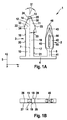
- Fig. 1A
- einen Einpresskontakt mit einem Kontaktstift und einem Zentrierstift auf einen Sockel angeordnet und in einem eine x-, eine y- und eine z-Richtung aufspannenden Koordinatensystem in Seitenansicht,
- Fig. 1 B
- den Einpresskontakt mit dem Kontaktstift und dem Zentrierstift auf den Sockel angeordnet und das Koordinatensystem in Draufsicht,
- Fig. 1C
- eine Spitze des Kontaktstiftes in perspektivischer Darstellung,
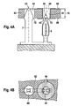
- Fig. 2A
- eine Leiterplatte mit einer ersten und einer zweiten Ausnehmung und den Einpresskontakt mit dem Kontaktstift und dem Zentrierstift während eines Einfädelvorganges des Kontaktstiftes in die erste Ausnehmung zu Beginn des Einfädelvorganges bei einem lateralen Versatz in x-Richtung in Seitenansicht,
- Fig. 2B
- die Leiterplatte mit der ersten und der zweiten Ausnehmung und den Einpresskontakt mit dem Kontaktstift und dem Zentrierstift während des Einfädelvorganges des Kontaktstiftes in die erste Ausnehmung zu Beginn des Einfädelvorganges bei dem lateralen Versatz in x-Richtung in Draufsicht,
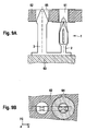
- Fig. 3A
- die Leiterplatte mit der ersten und der zweiten Ausnehmung und den Einpresskontakt mit dem Kontaktstift und dem Zentrierstift während des Einfädelvorganges des Kontaktstiftes in die erste Ausnehmung in einem fortgeschrittenem Stadium des Einfädelvorganges bei dem lateralen Versatz in x-Richtung in Seitenansicht,
- Fig. 3B
- die Leiterplatte mit der ersten und der zweiten Ausnehmung und den Einpresskontakt mit dem Kontaktstift und dem Zentrierstift während des Einfädelvorganges des Kontaktstiftes in die erste Ausnehmung in dem fortgeschrittenem Stadium des Einfädelvorganges bei dem lateralen Versatz in x-Richtung in Draufsicht,
- Fig. 4A
- die Leiterplatte mit der ersten und der zweiten Ausnehmung und den Einpresskontakt mit dem Kontaktstift und dem Zentrierstift während des Einfädelvorganges des Kontaktstiftes in die erste Ausnehmung in einem weiteren Stadium des Einfädelvorganges bei dem lateralen Versatz in x-Richtung in Seitenansicht,
- Fig. 4B
- die Leiterplatte mit der ersten und der zweiten Ausnehmung und den Einpresskontakt mit dem Kontaktstift und dem Zentrierstift während des Einfädelvorganges des Kontaktstiftes in die erste Ausnehmung in dem weiteren Stadium des Einfädelvorganges bei dem lateralen Versatz in x-Richtung in Draufsicht,
- Fig. 5A
- die Leiterplatte mit der ersten und der zweiten Ausnehmung und den Einpresskontakt mit dem Kontaktstift und dem Zentrierstift während des Einfädelvorganges des Kontaktstiftes in die erste Ausnehmung in einem vierten Stadium des Einfädelvorganges bei dem lateralen Versatz in x-Richtung in Seitenansicht,
- Fig. 5B
- die Leiterplatte mit der ersten und der zweiten Ausnehmung und den Einpresskontakt mit dem Kontaktstift und dem Zentrierstift während des Einfädelvorganges des Kontaktstiftes in die erste Ausnehmung in dem vierten Stadium des Einfädelvorganges bei dem lateralen Versatz in x-Richtung in Draufsicht,
- Fig. 6
- die Leiterplatte mit der ersten und der zweiten Ausnehmung und den Einpresskontakt mit dem Kontaktstift und dem Zentrierstift nach Erreichen der Betriebsposition des Kontaktstiftes in Seitenansicht,
- Fig. 7A
- die Leiterplatte mit der ersten und der zweiten Ausnehmung und den Einpresskontakt mit dem Kontaktstift und dem Zentrierstift während eines Einfädelvorganges des Kontaktstiftes in die erste Ausnehmung zu Beginn des Einfädelvorganges bei einem lateralen Versatz in y-Richtung in Seitenansicht,
- Fig. 7B
- die Leiterplatte mit der ersten und der zweiten Ausnehmung und den Einpresskontakt mit dem Kontaktstift und dem Zentrierstift während des Einfädelvorganges des Kontaktstiftes in die erste Ausnehmung zu-Beginn des Einfädelvorganges bei dem lateralen Versatz in y-Richtung in Draufsicht,
- Fig. 8A
- die Leiterplatte mit der ersten und der zweiten Ausnehmung und den Einpresskontakt mit dem Kontaktstift und dem Zentrierstift während des Einfädelvorganges des Kontaktstiftes in die erste Ausnehmung in einem fortgeschrittenem Stadium des Einfädelvorganges bei dem lateralen Versatz in y-Richtung in Seitenansicht,
- Fig. 8B
- die Leiterplatte mit der ersten und der zweiten Ausnehmung und den Einpresskontakt mit dem Kontaktstift und dem Zentrierstift während des Einfädelvorganges des Kontaktstiftes in die erste Ausnehmung in dem fortgeschrittenem Stadium des Einfädelvorganges bei dem lateralen Versatz in y-Richtung in Draufsicht,
- Fig. 9A
- die Leiterplatte mit der ersten und der zweiten Ausnehmung und den Einpresskontakt mit dem Kontaktstift und dem Zentrierstift während des Einfädelvorganges des Kontaktstiftes in die erste Ausnehmung in einem weiteren Stadium des Einfädelvorganges bei dem lateralen Versatz in y-Richtung in Seitenansicht,
- Fig. 9B
- die Leiterplatte mit der ersten und der zweiten Ausnehmung und den Einpresskontakt mit dem Kontaktstift und dem Zentrierstift während des Einfädelvorganges des Kontaktstiftes in die erste Ausnehmung in dem weiteren Stadium des Einfädelvorganges bei dem lateralen Versatz in y-Richtung in Draufsicht,
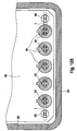
- Fig. 10A
- ein Gehäuse mit zwei jeweils einen Zentrierstift und einen Kontaktstift aufweisenden und an einer Schmalseite des Gehäuses angeordneten Einpresskontakten und eine Leiterplatte mit Ausnehmungen vor dem Einpressen der Kontaktstifte in zwei der Ausnehmungen von der Seite in Schnittdarstellung,
- Fig. 10B
- das Gehäuse mit den zwei jeweils den Zentrierstift und den Kontaktstift aufweisenden und an der Schmalseite des Gehäuses angeordneten Einpresskontakten und die Leiterplatte mit den Ausnehmungen vor dem Einpressen der Kontaktstifte in zwei der Ausnehmungen in Draufsicht,
- Fig. 11A
- ein weiteres Gehäuse mit zwei jeweils einen Zentrierstift und einen Kontaktstift aufweisenden und an zwei gegenüberliegenden Schmalseiten des Gehäuses angeordneten Einpresskontakten und eine Leiterplatte mit Ausnehmungen vor dem Einpressen der Kontaktstifte in zwei der Ausnehmungen von der Seite in Schnittdarstellung,
- Fig. 11 B
- das weitere Gehäuse mit den zwei jeweils einen Zentrierstift und einen Kontaktstift aufweisenden und an zwei gegenüberliegenden Schmalseiten des Gehäuses angeordneten Einpresskontakten und die Leiterplatte mit den Ausnehmungen vor dem Einpressen der Kontaktstifte in zwei der Ausnehmungen in Draufsicht,
- Fig. 12A
- ein drittes Gehäuse mit zwei jeweils einen Zentrierstift und einen Kontaktstift aufweisenden und an einer Schmalseite des Gehäuses angeordneten Einpresskontakten und drei Kontaktstiften und eine Leiterplatte mit sieben Ausnehmungen vor dem Einpressen der Kontaktstifte in fünf der Ausnehmungen von der Seite in Schnittdarstellung,
- Fig. 12B
- das dritte Gehäuse mit den zwei jeweils einen Zentrierstift und einen Kontaktstift aufweisenden und an der Schmalseite des Gehäuses angeordneten Einpresskontakten und den drei Kontaktstiften und die Leiterplatte mit den sieben Ausnehmungen vor dem Einpressen der Kontaktstifte in fünf der Ausnehmungen in Draufsicht.
- Fig. 13A
- zwei mittels eines Sockels verbundene Zentrierstifte und versetzt dazu zwei Kontaktstifte an einer Schmalseite eines vierten Gehäuses und eine Leiterplatte mit vier Ausnehmungen vor dem Einpressen der Kontaktstifte in zwei der Ausnehmungen von der Seite in Schnittdarstellung,
- Fig. 13B
- die zwei mittels eines Sockels verbundene Zentrierstifte und versetzt dazu die zwei Kontaktstifte an einer Schmalseite des vierten Gehäuses und die Leiterplatte mit den vier Ausnehmungen vor dem Einpressen der Kontaktstifte in zwei der Ausnehmungen in Seitenansicht und
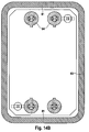
- Fig. 14A
- vier Kontaktstifte und zwei einzeln diametral gegenüberliegend angeordnete Zentrierstifte in einem Gehäuse und eine Leiterplatte mit sechs Ausnehmungen vor dem Einpressen der Kontaktstifte in vier der Ausnehmungen von der Seite in Schnittdarstellung,
- Fig. 14B
- die vier Kontaktstifte und die zwei einzeln diametral - - gegenüberliegend angeordnete Zentrierstifte in dem Gehäuse und die Leiterplatte mit sechs Ausnehmungen vor dem Einpressen der Kontaktstifte in vier der Ausnehmungen in Draufsicht,
- Fig. 1A
- a press-fit contact with a contact pin and a centering pin arranged on a pedestal and in an x-, y- and z-direction spanning coordinate system in side view,
- Fig. 1 B
- arranged the press-in contact with the contact pin and the centering pin on the base and the coordinate system in plan view,
- Fig. 1C
- a tip of the contact pin in a perspective view,
- Fig. 2A
- a printed circuit board having a first and a second recess and the press-in contact with the contact pin and the centering pin during a threading operation of the contact pin in the first recess at the beginning of the threading at a lateral offset in the x-direction in side view,
- Fig. 2B
- the printed circuit board with the first and the second recess and the press-in contact with the contact pin and the centering pin during the threading process of the contact pin in the first recess at the beginning of the threading at the lateral offset in the x direction in plan view,
- Fig. 3A
- the printed circuit board with the first and the second recess and the press-in contact with the contact pin and the centering pin during the threading operation of the contact pin in the first recess in an advanced stage of the threading at the lateral offset in the x-direction in side view,
- Fig. 3B
- the printed circuit board with the first and the second recess and the press-in contact with the contact pin and the centering pin during the threading process of the contact pin in the first recess in the advanced stage of the threading at the lateral offset in the x direction in plan view,
- Fig. 4A
- the printed circuit board with the first and the second recess and the press-in contact with the contact pin and the centering pin during the threading of the contact pin in the first Recess in a further stage of the threading process in the lateral offset in the x direction in side view,
- Fig. 4B
- the printed circuit board with the first and the second recess and the press-in contact with the contact pin and the centering pin during the threading process of the contact pin in the first recess in the further stage of Einfädelvorganges at the lateral offset in the x direction in plan view,
- Fig. 5A
- the printed circuit board with the first and the second recess and the press-in contact with the contact pin and the centering pin during the threading process of the contact pin in the first recess in a fourth stage of the threading at the lateral offset in the x-direction in side view,
- Fig. 5B
- the printed circuit board with the first and the second recess and the press-in contact with the contact pin and the centering pin during the threading process of the contact pin in the first recess in the fourth stage of threading at the lateral offset in the x direction in plan view,
- Fig. 6
- the circuit board with the first and the second recess and the press-in contact with the contact pin and the centering pin after reaching the operating position of the contact pin in side view,
- Fig. 7A
- the printed circuit board with the first and the second recess and the press-in contact with the contact pin and the centering pin during a threading operation of the contact pin in the first Recess at the beginning of the threading process with a lateral offset in the y-direction in side view,
- Fig. 7B
- the printed circuit board with the first and the second recess and the press-in contact with the contact pin and the centering pin during the threading process of the contact pin in the first recess at the beginning of the threading at the lateral offset in the y-direction in plan view,
- Fig. 8A
- the printed circuit board with the first and the second recess and the press-in contact with the contact pin and the centering pin during the threading of the contact pin in the first recess in an advanced stage of threading at the lateral offset in the y-direction in side view,
- Fig. 8B
- the printed circuit board with the first and the second recess and the press-in contact with the contact pin and the centering pin during the threading process of the contact pin in the first recess in the advanced stage of the threading at the lateral offset in the y-direction in plan view,
- Fig. 9A
- the printed circuit board with the first and the second recess and the press-in contact with the contact pin and the centering pin during the threading process of the contact pin in the first recess in a further stage of threading at the lateral offset in the y-direction in side view,
- Fig. 9B
- the circuit board with the first and the second recess and the press-in contact with the contact pin and the centering pin during the threading process of the contact pin in the first recess in the further stage of threading at the lateral offset in the y-direction in plan view,
- Fig. 10A
- a housing with two each having a centering pin and a contact pin and arranged on a narrow side of the housing press-fit and a printed circuit board with recesses before pressing the contact pins in two of the recesses from the side in a sectional view,
- Fig. 10B
- the housing with the two each having the centering pin and the contact pin and arranged on the narrow side of the housing press-fit and the circuit board with the recesses before pressing the contact pins in two of the recesses in plan view,
- Fig. 11A
- a further housing with two each having a centering pin and a contact pin and arranged on two opposite narrow sides of the housing press-fit and a circuit board with recesses before pressing the contact pins in two of the recesses from the side in a sectional view,
- Fig. 11B
- the further housing with the two each having a centering pin and a contact pin and arranged on two opposite narrow sides of the housing press-fit and the circuit board with the recesses before pressing the contact pins in two of the recesses in plan view,
- Fig. 12A
- a third housing with two each having a centering pin and a contact pin and arranged on a narrow side of the housing press-in contacts and three contact pins and a circuit board with seven recesses before pressing the contact pins in five of the recesses from the side in section,
- Fig. 12B
- the third housing with the two each having a centering pin and a contact pin and arranged on the narrow side of the housing press-fit and the three contact pins and the circuit board with the seven recesses before pressing the contact pins in five of the recesses in plan view.
- Fig. 13A
- two connected by a socket centering pins and offset to two pins on a narrow side of a fourth housing and a printed circuit board with four recesses before pressing the contact pins in two of the recesses from the side in a sectional view,
- Fig. 13B
- the two connected by a base centering pins and offset to the two pins on a narrow side of the fourth housing and the circuit board with the four recesses before pressing the contact pins in two of the recesses in side view and
- Fig. 14A
- four contact pins and two individually diametrically opposed centering pins in a housing and a circuit board with six recesses before pressing the contact pins in four of the recesses from the side in a sectional view,
- Fig. 14B
- the four contact pins and the two individually diametrically opposed centering pins in the housing and the circuit board with six recesses prior to the pressing in of the contact pins in four of the recesses in plan view,
In den verschiedenen Figuren sind ähnliche oder dieselben Elemente durch gleiche Bezugszeichen bezeichnet.In the various figures, similar or the same elements are designated by like reference numerals.
Der Zentrierstift 3 ist pfeilförmig mit einem quaderförmigen Schaft 10 und einer Spitze 11 ausgebildet. Der Schaft 10 und die Spitze 11 sind auch als Pfeilschaft 10 und Pfeilspitze 11 bezeichnet. Die Spitze 11 weist ein Unterteil 12 und ein geprägtes Oberteil 13 auf. Das geprägte Oberteil 13 der Spitze 11 weist begrenzende Prägungskanten 14, 15 auf, die Unterteil 12 und Oberteil 13 voneinander abgrenzen und einen Übergang definieren. Der Zentrierstift 3-weist-zwei einander abgewandte Schmalflächen 16, 17 und zwei einander abgewandte pfeilförmig ausgeformte Stirnflächen 18, 19 auf. Eine Breite einer jeden Schmalfläche 16, 17 ist durch die Tiefe des Einpresskontaktes 1 definiert. Jede der Schmalflächen 16, 17 untergliedert sich in eine Schaftschmalfläche 20, 21, eine Unterteilschmalfläche 22, 23 und eine Oberteilschmalfläche 24, 25. Die Schmalflächen 16, 17 und die Stirnflächen 18, 19 werden von Kanten 26 - 29 begrenzt. Die Pfeilspitze 11 ist in Richtung des Schaftes 10 aufgespreizt. Die Spreizung ist mittels der Zentrierpinachse 7 definiert. Die Spreizung ist symmetrisch zu der Zentrierpinachse 7. Die Spreizung ist gering und nimmt in einem oberen Pfeilspitzenteil 30 einen Winkel 31 zwischen 20° - 25°, insbesondere 22° zu der Zentrierpinachse 7 ein und in einem unteren Pfeilspitzenteil 32 auf einen Winkel 33 zwischen 15° - 22°, insbesondere 18° ab. Dabei wird ein eine größte Aufspreizung aufweisendes Pfeilspitzenteil 34, auch als ein einen größten Umfang aufweisendes Pfeilspitzenteil 34 oder als breiteste Stelle des Vorzentrierpins 3 bezeichnet, erreicht. Danach verjüngt sich die Pfeilspitze 11 und geht in den Pfeilschaft 10 über.The centering
Der Kontaktstift 2, auch als Kontaktpin 2 oder als Einpresspin 2 bezeichnet, weist einen quaderförmigen Schaft 41, einen quaderförmigen Kontaktteil 42 und eine Spitze 43 auf. Das Kontaktteil 42 weist eine schlitzförmige sich in Längsrichtung erstreckende Ausnehmung 44 auf und ist auch als Einpressteil 42 bezeichnet. Sich in Längsrichtung erstreckende Ränder 45 des quaderförmigen Kontaktteiles 42 sind gerundet. Der Kontaktstift 2 weist an der Spitze-43 ein oberes Ende 46 auf. Das quaderförmige Kontaktteil 42 des Kontaktpins 2 weist einen größeren Umfang als der Zentrierpinschaft 10 auf. Das quaderförmige Kontaktteil 42 erstreckt sich in Höhe des Zentrierpinschaftes 10 unterhalb des eine größte Aufspreizung aufweisenden Pfeilspitzenteils 34 und ist damit unterhalb des größten Umfangs des Zentrierpins 3 angeordnet. Die Kontaktstiftspitze 43 ist in Höhe des einen größten Umfang aufweisenden Pfeilspitzenteiles 34 angeordnet.The
In einem zweiten Stadium des Einfädelvorgangs hat das Pfeilspitzenende 53 des Zentrierstiftes 3 zwei Drittel der Ausnehmungsstrecke 70 innerhalb der zweiten Ausnehmung 65 zurückgelegt, wie in den
In einem dritten Stadium des Einfädelvorgangs hat das Zentrierpinpfeilspitzenteil 53 mit der größten Aufspreizung die Eingangsöffnung der Ausnehmung 65 erreicht und liegt an der Umfangskante 72 an, wie in den
In einem vierten Stadium des Einfädelvorgangs hat das Zentrierpinpfeilspitzenteil 53 mit der größten Aufspreizung zwei Drittel der Ausnehmungsstrecke 70 innerhalb der zweiten Ausnehmung 65 zurück gelegt, wie in den
In einem fünften Stadium des Einfädelvorgangs ist eine Einpressendposition der Leiterplatte 62 erreicht, wie in
Claims (11)
- Press-in contact (1) having a base (4), a contact pin (2) and a second pin (3) which extends parallel to the contact pin (2),
characterized in that- the second pin (3) projects beyond the contact pin (2),- with the second pin (3) having a shank (10) and a tip (11),- and the second pin (3) having a maximum circumference in the region (34) of its tip (11) which is arranged level with a tip (43) of the contact pin (2),- and the shank (10) of the second pin (3) having a smaller circumference than the region (34) of the tip (11) of the second pin (3) level with and over a length of a press-in part (42) of the contact pin (2). - Press-in contact according to Claim 1, characterized in that the second pin (3) has a smaller circumference than the press-in part (42) level with and over a length of a press-in part (42) of the contact pin (2).
- Press-in contact according to Claim 1, characterized in that the second pin (3) is in the form of an arrow with a cuboid shank (10) and a tip (11).
- Press-in contact according to Claim 2, characterized in that the press-in part (42) is elastic.
- Housing (63) having a contact pin (2) and a second pin (3) which extends parallel to the contact pin (2), characterized in that- the second pin (3) projects beyond the contact pin (2),- with the second pin (3) having a shank (10) and a tip (11),- and the second pin (3) having a maximum circumference in the region (34) of its tip (11) which is arranged level with a tip (43) of the contact pin (2),- and the shank (10) of the second pin having a smaller circumference than the region (34) of the tip (11) of the second pin (3) level with and over a length of a press-in part (42) of the contact pin (2).
- Housing (63) having a contact pin (2) and two further pins (3) which extend parallel to the contact pin (2), characterized in that- the two further pins (3) project beyond the contact pin (2),- with the further pins (3) each having a shank (10) and a tip (11),- and the further pins (3) each having a maximum circumference in the region (34) of their tip (11) which is arranged level with a tip (43) of the contact pin (2),- and the shank (10) of the further pins having a smaller circumference than the region (34) of the tips (11) of the further pins (3) level with and over a length of a press-in part (42) of the contact pin (2).
- Housing according to Claim 6, characterized in that the two further pins (3) are arranged on a base (4).
- Housing according to Claim 6 and/or 7, characterized in that the two further pins (3) are arranged at two different ends (82, 83) of a housing narrow side (81).
- Housing according to Claim 6, characterized in that the two further pins (3) are arranged diametrically on two opposite housing narrow sides (81).
- Method for inserting a printed circuit board (62) into a housing (63) having a contact pin (2) and a second pin (3) which extends parallel to the contact pin (2) and projects beyond the contact pin (2), with the second pin (3) having a shank (10) and a tip (11), and the second pin (3) having a maximum circumference in the region (34) of its tip (11) which is arranged level with a tip (43) of the contact pin (2), and the shank (10) of the second pin (3) having a smaller circumference than the region (34) of the tip (11) of the second pin (3) level with and over a length of a press-in part (42) of the contact pin (2), the said method comprising the following method steps:- the printed circuit board (62) is inserted into the housing (63) such that it can be displaced in the lateral direction by the second pin (3) such that a tip (43) of the contact pin (2) enters a recess (61) without making contact and- a press-in part (42) of the contact pin (2) is pressed into the printed circuit board (62).
- Printed circuit board (62) combined with a press-in contact (1) according to one or more of Claims 1-4 or with a housing (63) according to one or more of Claims 5-9, with the printed circuit board (62) being equipped with at least two recesses (61, 65), at least a first recess (61) of the said two recesses having a contact sleeve (64) for receiving a contact pin (2), and the second recess (65) for receiving a second or further pin (3) having a diameter which is 1.2 times to double the diameter, in particular 1.3 times the diameter, of the first recess (61).
Applications Claiming Priority (2)
| Application Number | Priority Date | Filing Date | Title |
|---|---|---|---|
| DE102008004882A DE102008004882A1 (en) | 2008-01-17 | 2008-01-17 | Press-in contact with a socket, a contact pin and a second pin |
| PCT/EP2008/067831 WO2009089981A1 (en) | 2008-01-17 | 2008-12-18 | Press-in contact having base, contact pin and second pin |
Publications (2)
| Publication Number | Publication Date |
|---|---|
| EP2235794A1 EP2235794A1 (en) | 2010-10-06 |
| EP2235794B1 true EP2235794B1 (en) | 2012-02-15 |
Family
ID=40427497
Family Applications (1)
| Application Number | Title | Priority Date | Filing Date |
|---|---|---|---|
| EP08871024A Active EP2235794B1 (en) | 2008-01-17 | 2008-12-18 | Press-in contact having base, contact pin and second pin |
Country Status (7)
| Country | Link |
|---|---|
| US (1) | US9166310B2 (en) |
| EP (1) | EP2235794B1 (en) |
| JP (1) | JP4940356B2 (en) |
| CN (1) | CN101911394B (en) |
| AT (1) | ATE545971T1 (en) |
| DE (1) | DE102008004882A1 (en) |
| WO (1) | WO2009089981A1 (en) |
Cited By (2)
| Publication number | Priority date | Publication date | Assignee | Title |
|---|---|---|---|---|
| DE102017120357A1 (en) | 2017-09-05 | 2019-03-07 | HELLA GmbH & Co. KGaA | Contact device for the electrical connection of two printed circuit boards |
| WO2020234478A1 (en) | 2019-05-23 | 2020-11-26 | Phoenix Contact Gmbh & Co. Kg | Assembly having a solder pin and a solder point |
Families Citing this family (17)
| Publication number | Priority date | Publication date | Assignee | Title |
|---|---|---|---|---|
| DE102009060739A1 (en) * | 2009-12-29 | 2011-07-14 | Sorig, Ludger, 59387 | Electrical press contact for transmission of electric current and/or signals, has three portions, where elasticity at one of portions measured with respect to longitudinal force is smaller than elasticity of insertion zone for lateral force |
| CN103250305A (en) * | 2010-12-16 | 2013-08-14 | Fci公司 | Contact pin, header connector and connector assembly |
| DE102011077915A1 (en) * | 2011-06-21 | 2012-12-27 | Robert Bosch Gmbh | Press-in pin for an electrical press-fit connection between an electronic component and a substrate plate |
| DE102013214621B4 (en) * | 2013-07-26 | 2018-09-20 | Continental Automotive Gmbh | Press-fit pin and component with a press-fit pin |
| JP5681261B1 (en) * | 2013-10-31 | 2015-03-04 | 株式会社フジクラ | PCB mounting terminals |
| JP2016027536A (en) * | 2014-06-27 | 2016-02-18 | 住友電装株式会社 | Printed board with terminal |
| JP6269451B2 (en) * | 2014-11-19 | 2018-01-31 | 株式会社デンソー | Electrical connection structure |
| US9246253B1 (en) * | 2014-11-26 | 2016-01-26 | Tyco Electronics Corporation | Connector with stabilization members and method of assembly |
| JP6451569B2 (en) * | 2015-09-14 | 2019-01-16 | 株式会社デンソー | Electronic equipment |
| JP6485367B2 (en) * | 2016-01-13 | 2019-03-20 | トヨタ自動車株式会社 | connector |
| DE102016212258B4 (en) * | 2016-07-05 | 2020-02-27 | Continental Automotive Gmbh | Combination comprising a plug and a threading aid, arrangement and method for attaching a plug to a printed circuit board |
| JP6711262B2 (en) * | 2016-12-26 | 2020-06-17 | 株式会社デンソー | Electronic device |
| JP7027932B2 (en) * | 2018-02-14 | 2022-03-02 | 住友電装株式会社 | Press-fit terminal |
| EP3544121B1 (en) * | 2018-03-19 | 2022-05-04 | Mahle International GmbH | Electrical heating device |
| DE102019218205A1 (en) * | 2019-11-25 | 2021-05-27 | Continental Teves Ag & Co. Ohg | Electronics housing for automated assembly |
| DE202020107455U1 (en) * | 2020-12-22 | 2022-03-29 | Andreas Veigel | PCB connector |
| EP4271152A1 (en) | 2022-04-27 | 2023-11-01 | FRONIUS INTERNATIONAL GmbH | Electronic assembly comprising at least one printed circuit board and external electronic components and inverter with such an electronic assembly |
Family Cites Families (19)
| Publication number | Priority date | Publication date | Assignee | Title |
|---|---|---|---|---|
| US3470529A (en) * | 1967-05-22 | 1969-09-30 | Heyman Mfg Co Inc | Tubular blade for electrical plug caps |
| DE3801352A1 (en) * | 1988-01-19 | 1989-07-27 | Standard Elektrik Lorenz Ag | Printed circuit board |
| US5215473A (en) * | 1992-05-05 | 1993-06-01 | Molex Incorporated | High speed guarded cavity backplane connector |
| US5468154A (en) * | 1993-12-15 | 1995-11-21 | Burndy Corporation | Multi-piece housing card edge connector with mounting arms |
| US5882214A (en) * | 1996-06-28 | 1999-03-16 | The Whitaker Corporation | Electrical connector with contact assembly |
| US6139373A (en) * | 1997-04-08 | 2000-10-31 | Thomas & Betts International, Inc. | Multi-pin electrical connectors |
| CN1104067C (en) * | 1997-04-17 | 2003-03-26 | 三星电子株式会社 | Cable connector and monitor equipped with the same |
| US6062916A (en) * | 1998-07-14 | 2000-05-16 | General Motors Corporation | Printed circuit board with pass through bussed terminal system for a bussed electrical distribution center |
| EP1171933B1 (en) | 1999-08-10 | 2007-12-12 | Panduit Corp. | Patch cord connector |
| DE10223382A1 (en) | 2002-05-25 | 2003-12-04 | Conti Temic Microelectronic | Press-in contact e.g. for PCB, includes narrow U-shaped slot made into base between pins |
| JP2004039742A (en) * | 2002-07-01 | 2004-02-05 | Tokai Rika Co Ltd | Temporarily fixing component |
| US6572404B1 (en) * | 2002-07-08 | 2003-06-03 | Hon Hai Precision Ind. Co., Ltd. | Board lock for electrical connector |
| US6648682B1 (en) * | 2002-07-24 | 2003-11-18 | Hon Hai Precision Ind. Co., Ltd. | Electrical connector having board locks |
| JP4082285B2 (en) * | 2003-06-13 | 2008-04-30 | 住友電装株式会社 | PCB connection structure |
| JP2006310069A (en) * | 2005-04-28 | 2006-11-09 | Tyco Electronics Amp Kk | Compliant pin and electrical component using it |
| CN2809949Y (en) * | 2005-06-10 | 2006-08-23 | 富士康(昆山)电脑接插件有限公司 | Backboard connector |
| DE102006011657A1 (en) | 2006-03-12 | 2007-09-20 | Kramski Gmbh | Contact pin and method for its manufacture |
| JP2008004345A (en) * | 2006-06-21 | 2008-01-10 | Toyota Motor Corp | Joint state inspection device of press fit connector, press fit device equipped with it, and joint state inspection method of press fit connector |
| US7549897B2 (en) * | 2006-08-02 | 2009-06-23 | Tyco Electronics Corporation | Electrical connector having improved terminal configuration |
-
2008
- 2008-01-17 DE DE102008004882A patent/DE102008004882A1/en not_active Withdrawn
- 2008-12-18 WO PCT/EP2008/067831 patent/WO2009089981A1/en active Application Filing
- 2008-12-18 AT AT08871024T patent/ATE545971T1/en active
- 2008-12-18 JP JP2010542555A patent/JP4940356B2/en active Active
- 2008-12-18 EP EP08871024A patent/EP2235794B1/en active Active
- 2008-12-18 US US12/812,546 patent/US9166310B2/en active Active
- 2008-12-18 CN CN2008801248897A patent/CN101911394B/en active Active
Cited By (2)
| Publication number | Priority date | Publication date | Assignee | Title |
|---|---|---|---|---|
| DE102017120357A1 (en) | 2017-09-05 | 2019-03-07 | HELLA GmbH & Co. KGaA | Contact device for the electrical connection of two printed circuit boards |
| WO2020234478A1 (en) | 2019-05-23 | 2020-11-26 | Phoenix Contact Gmbh & Co. Kg | Assembly having a solder pin and a solder point |
Also Published As
| Publication number | Publication date |
|---|---|
| WO2009089981A1 (en) | 2009-07-23 |
| ATE545971T1 (en) | 2012-03-15 |
| CN101911394A (en) | 2010-12-08 |
| US9166310B2 (en) | 2015-10-20 |
| JP2011510439A (en) | 2011-03-31 |
| EP2235794A1 (en) | 2010-10-06 |
| CN101911394B (en) | 2013-03-27 |
| JP4940356B2 (en) | 2012-05-30 |
| DE102008004882A1 (en) | 2009-07-23 |
| US20110039428A1 (en) | 2011-02-17 |
Similar Documents
| Publication | Publication Date | Title |
|---|---|---|
| EP2235794B1 (en) | Press-in contact having base, contact pin and second pin | |
| DE10321348B4 (en) | Connectors | |
| EP1754285B1 (en) | Press-in contact | |
| EP1730817B1 (en) | Contact element for pressing into a hole of a printed circuit board | |
| EP1821369B1 (en) | PCB plug-in extension | |
| DE102006011657A1 (en) | Contact pin and method for its manufacture | |
| EP3446366B1 (en) | Plug contact | |
| EP0059462B1 (en) | Pressurized connection pin | |
| DE102009025113A1 (en) | Press-in contact for connecting an electronic component to a printed circuit board and press-fit tool | |
| DE102019119588A1 (en) | Contact element for the electrical connection of circuit cards and method for assembling a circuit card arrangement | |
| EP0198408B1 (en) | Tool for manufacturing an electrical contact pin for printed-circuit boards | |
| EP2561582B1 (en) | Electrical plug contact | |
| DE102008024446A1 (en) | Connection element for use in surface mounted device-technology for connecting connector pin at printed circuit board, has sheet metal contact element lying at walls of inner space of cage element, and forming contact surface for pin | |
| DE102008014337A1 (en) | PCB connector | |
| DE3801352C2 (en) | ||
| EP1982387B1 (en) | Slimline sim block | |
| DE102007035325A1 (en) | Pin-shaped contact element and plug connection | |
| DE102014217927A1 (en) | Method for solderless electrical press-in contacting of electrically conductive press-fit pins in printed circuit boards | |
| DE102020104620B3 (en) | Contact element and circuit board with such a contact element | |
| EP0921594B1 (en) | Connection device | |
| EP3740050A1 (en) | Printed circuit board with a connector | |
| WO2009003907A1 (en) | Plug-type connector | |
| EP2696439A2 (en) | Electrical contact with cutting edge | |
| DE102019102668B3 (en) | Contact element and circuit board with such a contact element | |
| WO2014135557A1 (en) | Clip contact element for a printed circuit board, and method for producing same |
Legal Events
| Date | Code | Title | Description |
|---|---|---|---|
| PUAI | Public reference made under article 153(3) epc to a published international application that has entered the european phase |
Free format text: ORIGINAL CODE: 0009012 |
|
| 17P | Request for examination filed |
Effective date: 20100817 |
|
| AK | Designated contracting states |
Kind code of ref document: A1 Designated state(s): AT BE BG CH CY CZ DE DK EE ES FI FR GB GR HR HU IE IS IT LI LT LU LV MC MT NL NO PL PT RO SE SI SK TR |
|
| AX | Request for extension of the european patent |
Extension state: AL BA MK RS |
|
| DAX | Request for extension of the european patent (deleted) | ||
| REG | Reference to a national code |
Ref country code: DE Ref legal event code: R079 Ref document number: 502008006447 Country of ref document: DE Free format text: PREVIOUS MAIN CLASS: H01R0012320000 Ipc: H01R0012000000 |
|
| RIC1 | Information provided on ipc code assigned before grant |
Ipc: H01R 12/50 20110101ALI20110722BHEP Ipc: H01R 12/00 20060101AFI20110722BHEP |
|
| GRAP | Despatch of communication of intention to grant a patent |
Free format text: ORIGINAL CODE: EPIDOSNIGR1 |
|
| GRAS | Grant fee paid |
Free format text: ORIGINAL CODE: EPIDOSNIGR3 |
|
| GRAA | (expected) grant |
Free format text: ORIGINAL CODE: 0009210 |
|
| AK | Designated contracting states |
Kind code of ref document: B1 Designated state(s): AT BE BG CH CY CZ DE DK EE ES FI FR GB GR HR HU IE IS IT LI LT LU LV MC MT NL NO PL PT RO SE SI SK TR |
|
| REG | Reference to a national code |
Ref country code: GB Ref legal event code: FG4D Free format text: NOT ENGLISH Ref country code: CH Ref legal event code: EP |
|
| REG | Reference to a national code |
Ref country code: IE Ref legal event code: FG4D Free format text: LANGUAGE OF EP DOCUMENT: GERMAN |
|
| REG | Reference to a national code |
Ref country code: AT Ref legal event code: REF Ref document number: 545971 Country of ref document: AT Kind code of ref document: T Effective date: 20120315 |
|
| REG | Reference to a national code |
Ref country code: DE Ref legal event code: R096 Ref document number: 502008006447 Country of ref document: DE Effective date: 20120412 |
|
| REG | Reference to a national code |
Ref country code: NL Ref legal event code: VDEP Effective date: 20120215 |
|
| LTIE | Lt: invalidation of european patent or patent extension |
Effective date: 20120215 |
|
| PG25 | Lapsed in a contracting state [announced via postgrant information from national office to epo] |
Ref country code: IS Free format text: LAPSE BECAUSE OF FAILURE TO SUBMIT A TRANSLATION OF THE DESCRIPTION OR TO PAY THE FEE WITHIN THE PRESCRIBED TIME-LIMIT Effective date: 20120615 Ref country code: NO Free format text: LAPSE BECAUSE OF FAILURE TO SUBMIT A TRANSLATION OF THE DESCRIPTION OR TO PAY THE FEE WITHIN THE PRESCRIBED TIME-LIMIT Effective date: 20120515 Ref country code: HR Free format text: LAPSE BECAUSE OF FAILURE TO SUBMIT A TRANSLATION OF THE DESCRIPTION OR TO PAY THE FEE WITHIN THE PRESCRIBED TIME-LIMIT Effective date: 20120215 Ref country code: LT Free format text: LAPSE BECAUSE OF FAILURE TO SUBMIT A TRANSLATION OF THE DESCRIPTION OR TO PAY THE FEE WITHIN THE PRESCRIBED TIME-LIMIT Effective date: 20120215 Ref country code: NL Free format text: LAPSE BECAUSE OF FAILURE TO SUBMIT A TRANSLATION OF THE DESCRIPTION OR TO PAY THE FEE WITHIN THE PRESCRIBED TIME-LIMIT Effective date: 20120215 |
|
| PG25 | Lapsed in a contracting state [announced via postgrant information from national office to epo] |
Ref country code: PL Free format text: LAPSE BECAUSE OF FAILURE TO SUBMIT A TRANSLATION OF THE DESCRIPTION OR TO PAY THE FEE WITHIN THE PRESCRIBED TIME-LIMIT Effective date: 20120215 Ref country code: LV Free format text: LAPSE BECAUSE OF FAILURE TO SUBMIT A TRANSLATION OF THE DESCRIPTION OR TO PAY THE FEE WITHIN THE PRESCRIBED TIME-LIMIT Effective date: 20120215 Ref country code: PT Free format text: LAPSE BECAUSE OF FAILURE TO SUBMIT A TRANSLATION OF THE DESCRIPTION OR TO PAY THE FEE WITHIN THE PRESCRIBED TIME-LIMIT Effective date: 20120615 Ref country code: GR Free format text: LAPSE BECAUSE OF FAILURE TO SUBMIT A TRANSLATION OF THE DESCRIPTION OR TO PAY THE FEE WITHIN THE PRESCRIBED TIME-LIMIT Effective date: 20120516 Ref country code: FI Free format text: LAPSE BECAUSE OF FAILURE TO SUBMIT A TRANSLATION OF THE DESCRIPTION OR TO PAY THE FEE WITHIN THE PRESCRIBED TIME-LIMIT Effective date: 20120215 |
|
| REG | Reference to a national code |
Ref country code: IE Ref legal event code: FD4D |
|
| PG25 | Lapsed in a contracting state [announced via postgrant information from national office to epo] |
Ref country code: CY Free format text: LAPSE BECAUSE OF FAILURE TO SUBMIT A TRANSLATION OF THE DESCRIPTION OR TO PAY THE FEE WITHIN THE PRESCRIBED TIME-LIMIT Effective date: 20120215 |
|
| REG | Reference to a national code |
Ref country code: HU Ref legal event code: AG4A Ref document number: E013882 Country of ref document: HU |
|
| PG25 | Lapsed in a contracting state [announced via postgrant information from national office to epo] |
Ref country code: IE Free format text: LAPSE BECAUSE OF FAILURE TO SUBMIT A TRANSLATION OF THE DESCRIPTION OR TO PAY THE FEE WITHIN THE PRESCRIBED TIME-LIMIT Effective date: 20120215 Ref country code: SE Free format text: LAPSE BECAUSE OF FAILURE TO SUBMIT A TRANSLATION OF THE DESCRIPTION OR TO PAY THE FEE WITHIN THE PRESCRIBED TIME-LIMIT Effective date: 20120215 Ref country code: CZ Free format text: LAPSE BECAUSE OF FAILURE TO SUBMIT A TRANSLATION OF THE DESCRIPTION OR TO PAY THE FEE WITHIN THE PRESCRIBED TIME-LIMIT Effective date: 20120215 Ref country code: EE Free format text: LAPSE BECAUSE OF FAILURE TO SUBMIT A TRANSLATION OF THE DESCRIPTION OR TO PAY THE FEE WITHIN THE PRESCRIBED TIME-LIMIT Effective date: 20120215 Ref country code: DK Free format text: LAPSE BECAUSE OF FAILURE TO SUBMIT A TRANSLATION OF THE DESCRIPTION OR TO PAY THE FEE WITHIN THE PRESCRIBED TIME-LIMIT Effective date: 20120215 Ref country code: SI Free format text: LAPSE BECAUSE OF FAILURE TO SUBMIT A TRANSLATION OF THE DESCRIPTION OR TO PAY THE FEE WITHIN THE PRESCRIBED TIME-LIMIT Effective date: 20120215 Ref country code: RO Free format text: LAPSE BECAUSE OF FAILURE TO SUBMIT A TRANSLATION OF THE DESCRIPTION OR TO PAY THE FEE WITHIN THE PRESCRIBED TIME-LIMIT Effective date: 20120215 |
|
| PG25 | Lapsed in a contracting state [announced via postgrant information from national office to epo] |
Ref country code: SK Free format text: LAPSE BECAUSE OF FAILURE TO SUBMIT A TRANSLATION OF THE DESCRIPTION OR TO PAY THE FEE WITHIN THE PRESCRIBED TIME-LIMIT Effective date: 20120215 |
|
| PLBE | No opposition filed within time limit |
Free format text: ORIGINAL CODE: 0009261 |
|
| STAA | Information on the status of an ep patent application or granted ep patent |
Free format text: STATUS: NO OPPOSITION FILED WITHIN TIME LIMIT |
|
| 26N | No opposition filed |
Effective date: 20121116 |
|
| REG | Reference to a national code |
Ref country code: DE Ref legal event code: R097 Ref document number: 502008006447 Country of ref document: DE Effective date: 20121116 |
|
| PG25 | Lapsed in a contracting state [announced via postgrant information from national office to epo] |
Ref country code: ES Free format text: LAPSE BECAUSE OF FAILURE TO SUBMIT A TRANSLATION OF THE DESCRIPTION OR TO PAY THE FEE WITHIN THE PRESCRIBED TIME-LIMIT Effective date: 20120526 |
|
| BERE | Be: lapsed |
Owner name: ROBERT BOSCH G.M.B.H. Effective date: 20121231 |
|
| PG25 | Lapsed in a contracting state [announced via postgrant information from national office to epo] |
Ref country code: MC Free format text: LAPSE BECAUSE OF NON-PAYMENT OF DUE FEES Effective date: 20121231 Ref country code: BG Free format text: LAPSE BECAUSE OF FAILURE TO SUBMIT A TRANSLATION OF THE DESCRIPTION OR TO PAY THE FEE WITHIN THE PRESCRIBED TIME-LIMIT Effective date: 20120515 |
|
| REG | Reference to a national code |
Ref country code: CH Ref legal event code: PL |
|
| PG25 | Lapsed in a contracting state [announced via postgrant information from national office to epo] |
Ref country code: BE Free format text: LAPSE BECAUSE OF NON-PAYMENT OF DUE FEES Effective date: 20121231 |
|
| PG25 | Lapsed in a contracting state [announced via postgrant information from national office to epo] |
Ref country code: LI Free format text: LAPSE BECAUSE OF NON-PAYMENT OF DUE FEES Effective date: 20121231 Ref country code: CH Free format text: LAPSE BECAUSE OF NON-PAYMENT OF DUE FEES Effective date: 20121231 |
|
| PG25 | Lapsed in a contracting state [announced via postgrant information from national office to epo] |
Ref country code: MT Free format text: LAPSE BECAUSE OF FAILURE TO SUBMIT A TRANSLATION OF THE DESCRIPTION OR TO PAY THE FEE WITHIN THE PRESCRIBED TIME-LIMIT Effective date: 20120215 |
|
| PG25 | Lapsed in a contracting state [announced via postgrant information from national office to epo] |
Ref country code: TR Free format text: LAPSE BECAUSE OF FAILURE TO SUBMIT A TRANSLATION OF THE DESCRIPTION OR TO PAY THE FEE WITHIN THE PRESCRIBED TIME-LIMIT Effective date: 20120215 |
|
| PG25 | Lapsed in a contracting state [announced via postgrant information from national office to epo] |
Ref country code: LU Free format text: LAPSE BECAUSE OF NON-PAYMENT OF DUE FEES Effective date: 20121218 |
|
| REG | Reference to a national code |
Ref country code: AT Ref legal event code: MM01 Ref document number: 545971 Country of ref document: AT Kind code of ref document: T Effective date: 20131218 |
|
| PG25 | Lapsed in a contracting state [announced via postgrant information from national office to epo] |
Ref country code: AT Free format text: LAPSE BECAUSE OF NON-PAYMENT OF DUE FEES Effective date: 20131218 |
|
| REG | Reference to a national code |
Ref country code: FR Ref legal event code: PLFP Year of fee payment: 8 |
|
| REG | Reference to a national code |
Ref country code: FR Ref legal event code: PLFP Year of fee payment: 9 |
|
| REG | Reference to a national code |
Ref country code: FR Ref legal event code: PLFP Year of fee payment: 10 |
|
| PGFP | Annual fee paid to national office [announced via postgrant information from national office to epo] |
Ref country code: IT Payment date: 20221230 Year of fee payment: 15 Ref country code: DE Payment date: 20230223 Year of fee payment: 15 |
|
| P01 | Opt-out of the competence of the unified patent court (upc) registered |
Effective date: 20230509 |
|
| PGFP | Annual fee paid to national office [announced via postgrant information from national office to epo] |
Ref country code: GB Payment date: 20231220 Year of fee payment: 16 |
|
| PGFP | Annual fee paid to national office [announced via postgrant information from national office to epo] |
Ref country code: HU Payment date: 20231211 Year of fee payment: 16 Ref country code: FR Payment date: 20231220 Year of fee payment: 16 |