EP2235732B1 - The field emission device with fine local dimming - Google Patents
The field emission device with fine local dimming Download PDFInfo
- Publication number
- EP2235732B1 EP2235732B1 EP08861270.0A EP08861270A EP2235732B1 EP 2235732 B1 EP2235732 B1 EP 2235732B1 EP 08861270 A EP08861270 A EP 08861270A EP 2235732 B1 EP2235732 B1 EP 2235732B1
- Authority
- EP
- European Patent Office
- Prior art keywords
- cathode
- substrate
- interconnections
- electrode
- fed
- Prior art date
- Legal status (The legal status is an assumption and is not a legal conclusion. Google has not performed a legal analysis and makes no representation as to the accuracy of the status listed.)
- Not-in-force
Links
- 239000000758 substrate Substances 0.000 claims description 64
- 238000000034 method Methods 0.000 claims description 22
- 239000000919 ceramic Substances 0.000 claims description 13
- 239000000463 material Substances 0.000 claims description 10
- 238000010894 electron beam technology Methods 0.000 claims description 8
- 125000006850 spacer group Chemical group 0.000 claims description 5
- 238000007650 screen-printing Methods 0.000 claims description 4
- 238000007789 sealing Methods 0.000 claims description 4
- 239000011521 glass Substances 0.000 claims description 2
- SWPMTVXRLXPNDP-UHFFFAOYSA-N 4-hydroxy-2,6,6-trimethylcyclohexene-1-carbaldehyde Chemical compound CC1=C(C=O)C(C)(C)CC(O)C1 SWPMTVXRLXPNDP-UHFFFAOYSA-N 0.000 claims 2
- 239000002134 carbon nanofiber Substances 0.000 claims 2
- OKTJSMMVPCPJKN-UHFFFAOYSA-N Carbon Chemical compound [C] OKTJSMMVPCPJKN-UHFFFAOYSA-N 0.000 claims 1
- 150000001722 carbon compounds Chemical class 0.000 claims 1
- 239000002041 carbon nanotube Substances 0.000 claims 1
- 229910021393 carbon nanotube Inorganic materials 0.000 claims 1
- VNWKTOKETHGBQD-UHFFFAOYSA-N methane Chemical compound C VNWKTOKETHGBQD-UHFFFAOYSA-N 0.000 claims 1
- 238000010586 diagram Methods 0.000 description 8
- 238000004519 manufacturing process Methods 0.000 description 3
- 238000003491 array Methods 0.000 description 2
- 238000010276 construction Methods 0.000 description 2
- 230000001934 delay Effects 0.000 description 2
- 239000012212 insulator Substances 0.000 description 2
- 239000004973 liquid crystal related substance Substances 0.000 description 2
- 239000002245 particle Substances 0.000 description 2
- 239000004065 semiconductor Substances 0.000 description 2
- 230000005540 biological transmission Effects 0.000 description 1
- 230000001419 dependent effect Effects 0.000 description 1
- 238000007599 discharging Methods 0.000 description 1
- 230000000694 effects Effects 0.000 description 1
- 230000005669 field effect Effects 0.000 description 1
- 238000004020 luminiscence type Methods 0.000 description 1
- 238000004080 punching Methods 0.000 description 1
- 230000001360 synchronised effect Effects 0.000 description 1
- 239000010409 thin film Substances 0.000 description 1
- 230000000007 visual effect Effects 0.000 description 1
Images

Classifications
-
- H—ELECTRICITY
- H01—ELECTRIC ELEMENTS
- H01J—ELECTRIC DISCHARGE TUBES OR DISCHARGE LAMPS
- H01J1/00—Details of electrodes, of magnetic control means, of screens, or of the mounting or spacing thereof, common to two or more basic types of discharge tubes or lamps
- H01J1/02—Main electrodes
- H01J1/30—Cold cathodes, e.g. field-emissive cathode
- H01J1/304—Field-emissive cathodes
-
- H—ELECTRICITY
- H01—ELECTRIC ELEMENTS
- H01J—ELECTRIC DISCHARGE TUBES OR DISCHARGE LAMPS
- H01J17/00—Gas-filled discharge tubes with solid cathode
- H01J17/38—Cold-cathode tubes
- H01J17/48—Cold-cathode tubes with more than one cathode or anode, e.g. sequence-discharge tube, counting tube, dekatron
- H01J17/49—Display panels, e.g. with crossed electrodes, e.g. making use of direct current
-
- H—ELECTRICITY
- H01—ELECTRIC ELEMENTS
- H01J—ELECTRIC DISCHARGE TUBES OR DISCHARGE LAMPS
- H01J2201/00—Electrodes common to discharge tubes
- H01J2201/30—Cold cathodes
-
- H—ELECTRICITY
- H01—ELECTRIC ELEMENTS
- H01J—ELECTRIC DISCHARGE TUBES OR DISCHARGE LAMPS
- H01J2329/00—Electron emission display panels, e.g. field emission display panels
- H01J2329/02—Electrodes other than control electrodes
- H01J2329/04—Cathode electrodes
- H01J2329/0407—Field emission cathodes
- H01J2329/0439—Field emission cathodes characterised by the emitter material
- H01J2329/0444—Carbon types
- H01J2329/0455—Carbon nanotubes (CNTs)
Definitions
- the present invention relates to a field emission device (FED) capable of fine local dimming, and more particularly, to a FED capable of fine local dimming, in which a multilayered interconnection is formed on a cathode substrate to supply a current to a plurality of cathode blocks.
- FED field emission device
- FPDs flat panel displays
- emissive displays may be classified into emissive displays and non-emissive displays.
- the emissive displays may be cathode ray tubes (CRTs), plasma display panels (PDPs), and field emission displays (FEDs), and the non-emissive displays may be liquid crystal displays (LCDs).
- CTRs cathode ray tubes
- PDPs plasma display panels
- FEDs field emission displays
- LCDs liquid crystal displays
- an LCD is lightweight and consumes low power
- the LCD is a non-emissive display that cannot be self-luminescent but receives external light to form an image so that an object cannot be observed using the LCD in a dark place.
- a backlight unit (BLU) is installed on a rear surface of the LCD.
- Conventional BLUs may employ cold cathode fluorescent lamps (CCFLs) functioning as linear light sources and light emitting diodes (LEDs) functioning as point light sources.
- CCFLs cold cathode fluorescent lamps
- LEDs light emitting diodes
- field emission BLUs having planar emissive structures have been developed in order to solve the above-described problems.
- the field emission BLUs consume low power and exhibit comparatively uniform luminance over large emission regions.
- a field emission BLU includes a cathode substrate having a field emitter and an anode substrate having a fluorescent material, which are disposed a predetermined distance apart from each other and opposite to each other and vacuum-packaged, so that electrons emitted from the field emitter collide with the fluorescent material of the anode substrate to cause cathode luminescence of the fluorescent material.
- FIG. 1 illustrates a conventional FED.
- an anode electrode 110 is disposed on one surface of an anode substrate 100, and a fluorescent material 120 is disposed on one surface of the anode electrode 110.
- a cathode electrode 210 is disposed on one surface of a cathode substrate 200, and field emitters 220 are disposed on a first substrate of the cathode electrode 210.
- a gate electrode 400 is disposed over the cathode substrate 200 on which the cathode electrode 210 and the field emitters 220 are disposed. Each of the field emitters 220 is exposed through an inclined opening 400a of the gate electrode 400 opposite to the fluorescent material 120.
- a plurality of first spacers 310 are disposed between the gate electrode 400 and the anode electrode 110, and a plurality of second spacers 320 are disposed between the gate electrode 400 and the cathode electrode 210.
- a CCFL having the above-described construction operates at low speed, thus precluding partial dimming or pulse driving. Furthermore, there is a specific limit for increasing a contrast ratio or eliminating a residual image from a dynamic picture.
- a BLU using an LED controls luminance or drives pulses according to an image displayed on a picture so as to obtain a high contrast ratio and a clear moving image.
- the BLU using the LED requires a high fabrication cost and complicated driver circuits.
- the BLU using the LED has a relatively short lifetime and hinders surface emission.
- a field emission lamp capable of standard local dimming has only a limited number of cathode blocks, thereby hindering fine local dimming.
- WO 01/93302 A1 discloses a field emission device for a visual display.
- the field emission device comprises a substrate and an emission layer on one face of the substrate.
- the emission layer has a multiplicity of emitters and gates, arranged as an array of emission pixels and conductive connections in the emission layer to the emitters and the gates.
- the substrate has conductive vias provided through the substrate or at least a front layer thereof to at least some of the said conductive connections in the emission layer for electrical connection to their emitters and gates.
- the substrate is further disclosed to include at least one ceramic layer supporting the emission layer and having the front layer vias and at least one deposited dielectric layer and at least one deposited metallic layer, wherein the deposited dielectric layer provides via apertures therethrough, and the metallic layer provides via connections across the dielectric layer and interconnections between the vias in the adjoining layers.
- US 5 726 530 A discloses a cold cathode field emission display whose resolution is not limited by the provision of individual ballast resistors for each pixel or by the wiring system used to deliver voltage to the cold cathodes.
- the cold cathode field emission display is provided with additional layers beneath the cold cathodes arrays so that said resistors and voltage delivery systems are located directly below the cold cathode arrays instead of alongside of them.
- KR 2002 0057639 A discloses a field emission display device with which the screen size of a display device and an emission current can be increased.
- an electron supplied from a lower electrode is dispersed through a conductive layer and an emitting layer, accelerated and emitted into vacuum through an upper electrode, and then accelerated by a voltage applied to an anode, thereby exciting a fluorescent material.
- the emitting layer is provided with a conductive particle surrounded by an insulator with a discontinuity.
- the conductive particle and the insulator are layered in the form of a multi-layer.
- the present invention is directed to a field emission device (FED) capable of fine local dimming, in which a multilayered cathode substrate is prepared and a multilayered interconnection is disposed on each cathode substrate so that fine local dimming is enabled using a plurality of cathode blocks without limiting the number of the cathode blocks.
- FED field emission device
- a field emission device capable of fine local dimming.
- the FED includes: an anode substrate including an anode electrode and a fluorescent material disposed on one surface of the anode substrate; a cathode substrate disposed opposite to the anode substrate and including a plurality of cathode electrodes and a field emitter disposed on one surface of the cathode substrate; and a gate electrode interposed between the anode substrate and the cathode substrate, wherein the cathode electrodes are blocked to configure in a plurality of cathode blocks according to sub-pixels or specific regions, and the cathode substrate is formed in a multi-layered structure so that a plurality of interconnections for connecting the respective cathode blocks with external electrodes are stacked in a multi-layered structure on the cathode substrate of each layer.
- a current control signal When a current control signal is applied to the cathode block corresponding to a specific region to enable fine local dimming of the specific region, only a specific region of the anode substrate may emit light by controlling electron beams of the cathode block.
- the amount of the electron beams emitted from the field emitter may be controlled using a plurality of cathode electrodes included in the cathode block so that only the specific region of the anode substrate emits light.
- the interconnections may be stacked and arranged on the cathode substrate of each layer through internal electrodes and via holes.
- the linewidths of the interconnections and the diameters of the via holes may be controlled so that current control signals are simultaneously transmitted to the respective cathode blocks.
- the cathode substrate including a plurality of cathode layers may be provided and a plurality of interconnections may be stacked on the respective cathode layers using one selected from the group consisting of a low-temperarure co-fired ceramic (LTCC) technique, a high-temperature co-fired ceramic (HTCC) technique, and a multilayer screen printing technique.
- LTCC low-temperarure co-fired ceramic
- HTCC high-temperature co-fired ceramic
- a cathode substrate includes a plurality of cathode layers, and a plurality of interconnections are disposed on each of the cathode layers so that a FED capable of fine local dimming can be embodied using a plurality of cathode blocks without limiting the number of the cathode blocks.
- a technical limit for local dimming of the FED can be overcome, the FED can obtain a high contrast ratio and enable reproduction of clear moving images.
- FED field emission device
- FIG. 2 is a schematic diagram of a FED capable of local dimming
- FIG. 3 is a schematic diagram of a FED in which m ⁇ n cathode blocks are formed to enable fine local dimming.
- a plurality of cathode electrodes 210 are blocked and included in cathode blocks CB according to sub-pixels or specific regions.
- the amount of current supplied to each of the cathode blocks CB may be controlled using a semiconductor switching circuit (not shown), such as a thin film transistor (TFT) or a metal-oxide-semiconductor field effect transistor (MOSFET). Also, the amount of current supplied to the cathode block CB may be controlled using a pulse width modulation (PWM) method or a pulse amplitude modulation (PAM) method.
- a semiconductor switching circuit not shown
- TFT thin film transistor
- MOSFET metal-oxide-semiconductor field effect transistor
- PWM pulse width modulation
- PAM pulse amplitude modulation
- a liquid crystal display requires finer local dimming in order to obtain UD (Ultra Definition) output and a high contrast ratio and solve a residual image during reproduction of moving images. Accordingly, the greatest possible number of cathode blocks CB must be ensured as shown in FIG. 3 .
- the cathode blocks CB must be disposed as adjacently as possible in order to prevent arcing caused by unnecessary charging/discharging of electrons emitted from the field emitter 220.
- the cathode substrate 200 is embodied as a single substrate, the interconnections L must be formed to have very fine linewidths so that mxn cathode blocks CB can be connected to mxn external electrodes E.
- the interconnections L when the interconnections L are formed to have the very fine linewidths, the interconnections L not only have high resistances, but also high resistance differences there between, so that a current control signal for controlling each of the cathode blocks CB may not reach a desired point in time due to a resistance-capacitance (RC) delay difference.
- RC resistance-capacitance
- a typical FED capable of local dimming has limited number of cathode blocks CB, thereby precluding fine local dimming.
- a multilayered cathode substrate is provided and a plurality of interconnections are stacked on each cathode substrate so that fine local dimming is enabled using a plurality of cathode blocks without limiting the number of the cathode blocks as will now be described in more detail.
- FIG. 4 is a diagram for explaining the characteristics of a FED according to an exemplary embodiment.
- a cathode substrate 200a includes a plurality of cathode substrates 200.
- An interconnection L for connecting each of cathode blocks CB with an external electrode E is stacked on each of the cathode substrates 200.
- the interconnections L are stacked and arranged on the respective cathode substrates 200 through internal electrodes 201 and via holes 202.
- any number of cathode blocks CB can be embodied according to the number of the cathode substrates 200, thus enabling fine local dimming.
- a FED can synchronize RC delays of the respective cathode blocks CB by controlling the linewidths of the interconnections L and the diameters of the via holes 202.
- current control signals may be simultaneously transmitted to the respective cathode blocks CB.
- the multilayered cathode substrate 200a and the multilayered interconnection L may be provided using the following methods.
- a technique of forming a multilayered structure such as a low-temperature cofired ceramic (LTCC) technique or a high-temperature co-fired ceramic (HTCC) technique, may be employed.
- LTCC low-temperature cofired ceramic
- HTCC high-temperature co-fired ceramic
- the internal electrode 201 and the via hole 202 are formed in each of bulk ceramic layers, which are called “Green sheets,” using punching and screen printing processes, and the bulk ceramic layers are laminated and fired.
- an LTCC technique is performed using an Ag electrode and an Ag/Pd electrode
- an HTCC technique is performed using a W electrode
- a ceramic substrate is used for both the LTCC and HTCC techniques.
- the LTCC technique may be performed at a temperature of about 900°C
- the HTCC technique may be performed at a temperature of about 1600°C.
- the ceramic substrate may have a thickness of about minimum 10 ⁇ m or more.
- each ceramic substrate may be used as an external substrate for vacuum sealing or bonded to a glass substrate appropriate for vacuum sealing.
- the internal electrode 201 and the via hole 202 are printed on each insulating layer, dried, and printed again so that an interconnection is stacked on each cathode substrate.
- FIG. 5 is a diagram for explaining fine local dimming operation of a FED according to an exemplary embodiment.
- a specific region of an anode substrate 100 may emit light by controlling electron beams of each of cathode blocks CB.
- an HD or UD LCD is embodied using a FED
- very fine local dimming is enabled and can even come up to the level of the resolution of an LCD.
- the FED can obtain a high contrast ratio and eliminate a residual image during reproduction of moving images.
Landscapes
- Cathode-Ray Tubes And Fluorescent Screens For Display (AREA)
- Discharge Lamps And Accessories Thereof (AREA)
- Control Of Indicators Other Than Cathode Ray Tubes (AREA)
Description
- The present invention relates to a field emission device (FED) capable of fine local dimming, and more particularly, to a FED capable of fine local dimming, in which a multilayered interconnection is formed on a cathode substrate to supply a current to a plurality of cathode blocks.
- In general, flat panel displays (FPDs) may be classified into emissive displays and non-emissive displays.
- The emissive displays may be cathode ray tubes (CRTs), plasma display panels (PDPs), and field emission displays (FEDs), and the non-emissive displays may be liquid crystal displays (LCDs).
- Although an LCD is lightweight and consumes low power, the LCD is a non-emissive display that cannot be self-luminescent but receives external light to form an image so that an object cannot be observed using the LCD in a dark place. In order to solve this problem, a backlight unit (BLU) is installed on a rear surface of the LCD.
- Conventional BLUs may employ cold cathode fluorescent lamps (CCFLs) functioning as linear light sources and light emitting diodes (LEDs) functioning as point light sources.
- However, complicated constructions of BLUs have led to a rise in fabrication costs. Also, since a light source is disposed on a side of a BLU, power consumption increases due to reflection and transmission of light. Above all, it is difficult to ensure uniformity of luminance due to on-going scaling-up of LCDs.
- In recent years, field emission BLUs having planar emissive structures have been developed in order to solve the above-described problems. Compared with conventional BLUs using CCFLs, the field emission BLUs consume low power and exhibit comparatively uniform luminance over large emission regions.
- Conventionally, a field emission BLU includes a cathode substrate having a field emitter and an anode substrate having a fluorescent material, which are disposed a predetermined distance apart from each other and opposite to each other and vacuum-packaged, so that electrons emitted from the field emitter collide with the fluorescent material of the anode substrate to cause cathode luminescence of the fluorescent material.
- The above-described conventional FED will now be described in more detail with reference to
FIG. 1 . -
FIG. 1 illustrates a conventional FED. - Referring to
FIG. 1 , ananode electrode 110 is disposed on one surface of ananode substrate 100, and afluorescent material 120 is disposed on one surface of theanode electrode 110. Acathode electrode 210 is disposed on one surface of acathode substrate 200, andfield emitters 220 are disposed on a first substrate of thecathode electrode 210. Agate electrode 400 is disposed over thecathode substrate 200 on which thecathode electrode 210 and thefield emitters 220 are disposed. Each of thefield emitters 220 is exposed through aninclined opening 400a of thegate electrode 400 opposite to thefluorescent material 120. Also, a plurality offirst spacers 310 are disposed between thegate electrode 400 and theanode electrode 110, and a plurality ofsecond spacers 320 are disposed between thegate electrode 400 and thecathode electrode 210. - When a predetermined drive voltage is applied to the
cathode electrode 210, thegate electrode 400, and theanode electrode 110, electron beams are radially emitted from thefield emitter 220. As a result, the electron beams emitted from thefield emitter 220 reach a portion of thefluorescent material 120 corresponding to the corresponding pixel to emit light. - On the other hand, a CCFL having the above-described construction operates at low speed, thus precluding partial dimming or pulse driving. Furthermore, there is a specific limit for increasing a contrast ratio or eliminating a residual image from a dynamic picture.
- In order to overcome the above-described drawbacks, a BLU using an LED controls luminance or drives pulses according to an image displayed on a picture so as to obtain a high contrast ratio and a clear moving image. However, the BLU using the LED requires a high fabrication cost and complicated driver circuits. In addition, the BLU using the LED has a relatively short lifetime and hinders surface emission.
- Therefore, a vast amount of research has been conducted on field emission lamps capable of local dimming in which a plurality of cathode electrodes are embodied as cathode blocks. However, when the number of the cathode blocks is increased to enable fine local dimming, interconnections between the cathode blocks and external electrodes become complicated.
- Owing to the above-described problems, a field emission lamp capable of standard local dimming has only a limited number of cathode blocks, thereby hindering fine local dimming.
-
WO 01/93302 A1 -
US 5 726 530 A discloses a cold cathode field emission display whose resolution is not limited by the provision of individual ballast resistors for each pixel or by the wiring system used to deliver voltage to the cold cathodes. The cold cathode field emission display is provided with additional layers beneath the cold cathodes arrays so that said resistors and voltage delivery systems are located directly below the cold cathode arrays instead of alongside of them. -
KR 2002 0057639 A - The present invention is directed to a field emission device (FED) capable of fine local dimming, in which a multilayered cathode substrate is prepared and a multilayered interconnection is disposed on each cathode substrate so that fine local dimming is enabled using a plurality of cathode blocks without limiting the number of the cathode blocks.
- The present invention is defined in the independent claim. The dependent claims define embodiments of the invention.
- A field emission device (FED) capable of fine local dimming is provided. The FED includes: an anode substrate including an anode electrode and a fluorescent material disposed on one surface of the anode substrate; a cathode substrate disposed opposite to the anode substrate and including a plurality of cathode electrodes and a field emitter disposed on one surface of the cathode substrate; and a gate electrode interposed between the anode substrate and the cathode substrate, wherein the cathode electrodes are blocked to configure in a plurality of cathode blocks according to sub-pixels or specific regions, and the cathode substrate is formed in a multi-layered structure so that a plurality of interconnections for connecting the respective cathode blocks with external electrodes are stacked in a multi-layered structure on the cathode substrate of each layer.
- When a current control signal is applied to the cathode block corresponding to a specific region to enable fine local dimming of the specific region, only a specific region of the anode substrate may emit light by controlling electron beams of the cathode block.
- Also, the amount of the electron beams emitted from the field emitter may be controlled using a plurality of cathode electrodes included in the cathode block so that only the specific region of the anode substrate emits light.
- The interconnections may be stacked and arranged on the cathode substrate of each layer through internal electrodes and via holes. The linewidths of the interconnections and the diameters of the via holes may be controlled so that current control signals are simultaneously transmitted to the respective cathode blocks.
- The cathode substrate including a plurality of cathode layers may be provided and a plurality of interconnections may be stacked on the respective cathode layers using one selected from the group consisting of a low-temperarure co-fired ceramic (LTCC) technique, a high-temperature co-fired ceramic (HTCC) technique, and a multilayer screen printing technique.
- According to the present invention, a cathode substrate includes a plurality of cathode layers, and a plurality of interconnections are disposed on each of the cathode layers so that a FED capable of fine local dimming can be embodied using a plurality of cathode blocks without limiting the number of the cathode blocks. As a result, since a technical limit for local dimming of the FED can be overcome, the FED can obtain a high contrast ratio and enable reproduction of clear moving images.
- Furthermore, since RC delays of the respective cathode blocks can be synchronized according to the design of the interconnections, current control signals can be simultaneously transmitted to the respective cathode blocks, thereby improving the characteristics of the FED.
-
-
FIG. 1 illustrates a conventional field emission device (FED). -
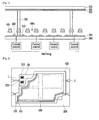
FIG. 2 is a schematic diagram of a FED capable of local dimming. -
FIG. 3 is a schematic diagram of a FED in which m×n cathode blocks are formed to enable fine local dimming. -
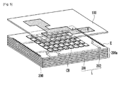
FIG. 4 is a diagram for explaining the characteristics of a FED according to an exemplary embodiment. -
FIG. 5 is a diagram for explaining fine local dimming operation of a FED according to an exemplary embodiment. -
- 100: Anode substrate
- 110: Anode electrode
- 120: Fluorescent material
- 200: Cathode substrate
- 210: Cathode electrode
- 220: field emitter
- 310, 320: Spacer
- 400: Gate
- L: Interconnection
- E: External electrode
- A field emission device (FED) capable of fine local dimming will be described more fully hereinafter with reference to the accompanying drawings, in which exemplary embodiments are shown.
- To facilitate understanding, a typical FED capable of local dimming will be briefly described.
-
FIG. 2 is a schematic diagram of a FED capable of local dimming, andFIG. 3 is a schematic diagram of a FED in which m×n cathode blocks are formed to enable fine local dimming. - Referring to
FIG. 2 , in the case of the FED capable of local dimming, a plurality ofcathode electrodes 210 are blocked and included in cathode blocks CB according to sub-pixels or specific regions. - That is, when a voltage applied to the
gate electrode 400 or theanode electrode 110 is fixed, amounts of electron beams emitted from afield emitter 220 through thecathode electrode 210 included in each of the cathode blocks CB are controlled by adjusting the amount of current supplied to the corresponding cathode block CB, so that local dimming is enabled. - The amount of current supplied to each of the cathode blocks CB may be controlled using a semiconductor switching circuit (not shown), such as a thin film transistor (TFT) or a metal-oxide-semiconductor field effect transistor (MOSFET). Also, the amount of current supplied to the cathode block CB may be controlled using a pulse width modulation (PWM) method or a pulse amplitude modulation (PAM) method.
- Meanwhile, a liquid crystal display (LCD) requires finer local dimming in order to obtain UD (Ultra Definition) output and a high contrast ratio and solve a residual image during reproduction of moving images. Accordingly, the greatest possible number of cathode blocks CB must be ensured as shown in
FIG. 3 . - As shown in
FIG. 2 , when only four cathode blocks CB are provided, a simple interconnection L for connecting an external electrode E and each of the cathode blocks CB is formed on a single plane. However, when the number of cathode blocks CB is increased in order to enable fine local dimming as shown inFIG. 3 , an increased number of interconnections L, that is, mxn interconnections L, are needed. As a result, connecting the interconnections L on a single plane becomes very complicated. - Furthermore, the cathode blocks CB must be disposed as adjacently as possible in order to prevent arcing caused by unnecessary charging/discharging of electrons emitted from the
field emitter 220. However, since thecathode substrate 200 is embodied as a single substrate, the interconnections L must be formed to have very fine linewidths so that mxn cathode blocks CB can be connected to mxn external electrodes E. - However, when the interconnections L are formed to have the very fine linewidths, the interconnections L not only have high resistances, but also high resistance differences there between, so that a current control signal for controlling each of the cathode blocks CB may not reach a desired point in time due to a resistance-capacitance (RC) delay difference.
- Owing to the foregoing problems, a typical FED capable of local dimming has limited number of cathode blocks CB, thereby precluding fine local dimming.
- In order to overcome the above-described problems, according to the present invention, a multilayered cathode substrate is provided and a plurality of interconnections are stacked on each cathode substrate so that fine local dimming is enabled using a plurality of cathode blocks without limiting the number of the cathode blocks as will now be described in more detail.
-
FIG. 4 is a diagram for explaining the characteristics of a FED according to an exemplary embodiment. - Referring to
FIG. 4 , in the FED, acathode substrate 200a includes a plurality ofcathode substrates 200. An interconnection L for connecting each of cathode blocks CB with an external electrode E is stacked on each of thecathode substrates 200. - The interconnections L are stacked and arranged on the
respective cathode substrates 200 throughinternal electrodes 201 and viaholes 202. - As described above, when the interconnection L for connecting the cathode block CB and the external electrode E is stacked on each of the
cathode substrates 200, arrangement of the interconnections L has a greatly increased degree of freedom. - In other words, even if a plurality of cathode blocks CB are provided, a plurality of interconnections L for connecting the respective cathode blocks CB and the external electrodes E can be stacked on the
respective cathode substrates 200. Therefore, any number of cathode blocks CB can be embodied according to the number of thecathode substrates 200, thus enabling fine local dimming. - In addition, a FED can synchronize RC delays of the respective cathode blocks CB by controlling the linewidths of the interconnections L and the diameters of the via holes 202. Thus, current control signals may be simultaneously transmitted to the respective cathode blocks CB.
- Meanwhile, the
multilayered cathode substrate 200a and the multilayered interconnection L may be provided using the following methods. - First, a technique of forming a multilayered structure, such as a low-temperature cofired ceramic (LTCC) technique or a high-temperature co-fired ceramic (HTCC) technique, may be employed.
- Specifically, the
internal electrode 201 and the viahole 202 are formed in each of bulk ceramic layers, which are called "Green sheets," using punching and screen printing processes, and the bulk ceramic layers are laminated and fired. - In general, an LTCC technique is performed using an Ag electrode and an Ag/Pd electrode, an HTCC technique is performed using a W electrode, and a ceramic substrate is used for both the LTCC and HTCC techniques. Also, the LTCC technique may be performed at a temperature of about 900°C, and the HTCC technique may be performed at a temperature of about 1600°C. The ceramic substrate may have a thickness of about minimum 10µm or more.
- In the LTCC or HTCC technique, each ceramic substrate may be used as an external substrate for vacuum sealing or bonded to a glass substrate appropriate for vacuum sealing.
- Second, a multilayer screen printing technique used for fabrication of typical plasma display panels (PDPs) may be adopted.
- Specifically, the
internal electrode 201 and the viahole 202 are printed on each insulating layer, dried, and printed again so that an interconnection is stacked on each cathode substrate. -
FIG. 5 is a diagram for explaining fine local dimming operation of a FED according to an exemplary embodiment. - Referring to
FIG. 5 , in the FED only a specific region of ananode substrate 100 may emit light by controlling electron beams of each of cathode blocks CB. - Accordingly, when an HD or UD LCD is embodied using a FED, very fine local dimming is enabled and can even come up to the level of the resolution of an LCD. Furthermore, the FED can obtain a high contrast ratio and eliminate a residual image during reproduction of moving images.
- While the invention has been shown and described with reference to certain exemplary embodiments thereof, it will be understood by those skilled in the art that various changes in form and details may be made therein without departing from the scope of the invention as defined by the appended claims.
Claims (9)
- A field emission device FED capable of fine local dimming, comprising:an anode substrate (100) including an anode electrode (110) and a fluorescent material (120) disposed on one surface of the anode substrate (100);a cathode substrate (200a) disposed opposite to the anode substrate (100) and including a plurality of cathode electrodes (210) and a field emitter (220) disposed on one surface of the cathode substrate (200); anda gate electrode (400) interposed between the anode substrate (100) and the cathode substrate (200),wherein the cathode electrodes (210) are blocked to configure in a plurality of cathode blocks (CB) according to sub-pixels or specific regions,the cathode substrate (200a) includes a plurality of cathode layers (200) and a plurality of interconnections (L), wherein the interconnections (L) are stacked on each of the cathode layers (200) so as to connect each of the cathode blocks (CB) with an external electrode (E),each of the plurality of interconnections (L) consist of internal electrodes (201) and connecting via holes (202), anda plurality of internal electrodes (201) is disposed on each of the plurality of cathode layers (200),characterized bythe plurality of internal electrodes (201) on at least one of the plurality of cathode layers (200) is arranged in a direction other than a direction of the plurality of internal electrodes (201) on an adjacent cathode layer (200).
- The FED according to claim 1, wherein, when a current control signal is applied to the cathode block (CB) corresponding to one of the specific region to enable fine local dimming of that specific region, only a specific region of the anode substrate (100) emits light by controlling electron beams of the cathode block (CB).
- The FED according to claim 2, wherein the amount of the electron beams emitted from the field emitter (220) is controlled using the plurality of cathode electrodes (210) included in the cathode block (CB) so that only the specific region of the anode substrate (100) emits light.
- The FED according to claim 1, wherein the interconnections (L) are stacked and arranged on the cathode substrate of each layer (200) through the internal electrodes (201) and the via holes (202).
- The FED according to claim 4, wherein linewidths of the interconnections (L) and diameters of the via holes (202) are controlled so that current control signals are simultaneously transmitted to the respective cathode blocks (CB).
- The FED according to claim 1, wherein the cathode substrate (200a) including the plurality of cathode layers (200) is provided and the plurality of interconnections (L) are stacked on the respective cathode layers using one selected from the group consisting of a low-temperature co-fired ceramic LTCC technique, a high- temperature co-fired ceramic HTCC technique, and a multilayer screen printing technique.
- The FED according to claim 6, wherein each ceramic layer used for the LTCC technique or the HTCC technique is used as an external substrate for vacuum sealing or bonded to a glass substrate appropriate for vacuum sealing.
- The FED according to claim 1, wherein a first spacer (310) is interposed between the anode electrode (110) and the gate electrode (400), and a second spacer (320) is interposed between the gate electrode (400) and the cathode electrode (210).
- The FED according to claim 1, wherein the field emitter (220) is formed of one selected from the group consisting of a carbon nanotube CNT, carbon nanofiber CNF, and a carbon compound.
Applications Claiming Priority (2)
| Application Number | Priority Date | Filing Date | Title |
|---|---|---|---|
| KR1020070132755A KR100868531B1 (en) | 2007-12-17 | 2007-12-17 | Fine local dimmable field emission device |
| PCT/KR2008/006521 WO2009078578A1 (en) | 2007-12-17 | 2008-11-06 | The field emission device with fine local dimming |
Publications (3)
| Publication Number | Publication Date |
|---|---|
| EP2235732A1 EP2235732A1 (en) | 2010-10-06 |
| EP2235732A4 EP2235732A4 (en) | 2011-04-20 |
| EP2235732B1 true EP2235732B1 (en) | 2014-04-16 |
Family
ID=40284161
Family Applications (1)
| Application Number | Title | Priority Date | Filing Date |
|---|---|---|---|
| EP08861270.0A Not-in-force EP2235732B1 (en) | 2007-12-17 | 2008-11-06 | The field emission device with fine local dimming |
Country Status (5)
| Country | Link |
|---|---|
| US (1) | US8129895B2 (en) |
| EP (1) | EP2235732B1 (en) |
| JP (1) | JP2011508375A (en) |
| KR (1) | KR100868531B1 (en) |
| WO (1) | WO2009078578A1 (en) |
Families Citing this family (2)
| Publication number | Priority date | Publication date | Assignee | Title |
|---|---|---|---|---|
| KR101605157B1 (en) | 2009-03-24 | 2016-03-22 | 삼성디스플레이 주식회사 | Method for driving display apparatus |
| KR102545211B1 (en) | 2018-01-10 | 2023-06-19 | 삼성전자주식회사 | Electronic apparatus and control method thereof |
Family Cites Families (18)
| Publication number | Priority date | Publication date | Assignee | Title |
|---|---|---|---|---|
| EP0364964B1 (en) * | 1988-10-17 | 1996-03-27 | Matsushita Electric Industrial Co., Ltd. | Field emission cathodes |
| JPH06124322A (en) * | 1992-10-12 | 1994-05-06 | Fujitsu Ltd | Wiring method for specified length net |
| US5686790A (en) * | 1993-06-22 | 1997-11-11 | Candescent Technologies Corporation | Flat panel device with ceramic backplate |
| US5591352A (en) * | 1995-04-27 | 1997-01-07 | Industrial Technology Research Institute | High resolution cold cathode field emission display method |
| US5644327A (en) * | 1995-06-07 | 1997-07-01 | David Sarnoff Research Center, Inc. | Tessellated electroluminescent display having a multilayer ceramic substrate |
| JPH1173898A (en) * | 1997-08-28 | 1999-03-16 | Futaba Corp | Field emission type image display device and its driving method |
| US6897855B1 (en) * | 1998-02-17 | 2005-05-24 | Sarnoff Corporation | Tiled electronic display structure |
| JP2000323078A (en) * | 1999-05-14 | 2000-11-24 | Ise Electronics Corp | Fluorescent display device |
| JP2001035352A (en) | 1999-07-22 | 2001-02-09 | Sharp Corp | Electron source, method of manufacturing the same, and image forming apparatus formed using the same |
| JP3502804B2 (en) * | 2000-03-17 | 2004-03-02 | 株式会社 ケイアンドティ | Method for growing carbon nanotubes and method for manufacturing electron gun and probe using the same |
| AU2001262499A1 (en) * | 2000-06-01 | 2001-12-11 | Complete Substrate Solutions Limited | Visual display |
| KR20020057639A (en) * | 2001-01-03 | 2002-07-12 | 엘지전자 주식회사 | Field emission display |
| US7557502B2 (en) * | 2001-10-18 | 2009-07-07 | Tpo Displays Corp. | Electroluminescent display with gas-tight enclosure |
| EP1315191B1 (en) * | 2001-11-23 | 2007-08-22 | Samsung SDI Co. Ltd. | Composite for paste including carbon nanotubes, electron emitting device using the same, and manufacturing method thereof |
| JP2006120479A (en) * | 2004-10-22 | 2006-05-11 | Hitachi Displays Ltd | Image display device |
| KR100652572B1 (en) | 2004-12-14 | 2006-12-01 | 엘지전자 주식회사 | Field emitter for backlight |
| KR20070050617A (en) | 2005-11-11 | 2007-05-16 | 엘지.필립스 엘시디 주식회사 | LCD Display |
| KR100748986B1 (en) * | 2006-01-23 | 2007-08-13 | 엘지.필립스 디스플레이 주식회사 | Multi-layered Electrode Structure of Flat Panel Display |
-
2007
- 2007-12-17 KR KR1020070132755A patent/KR100868531B1/en not_active Expired - Fee Related
-
2008
- 2008-11-06 US US12/741,253 patent/US8129895B2/en active Active
- 2008-11-06 JP JP2010539281A patent/JP2011508375A/en active Pending
- 2008-11-06 WO PCT/KR2008/006521 patent/WO2009078578A1/en not_active Ceased
- 2008-11-06 EP EP08861270.0A patent/EP2235732B1/en not_active Not-in-force
Also Published As
| Publication number | Publication date |
|---|---|
| EP2235732A4 (en) | 2011-04-20 |
| KR100868531B1 (en) | 2008-11-13 |
| US20100231119A1 (en) | 2010-09-16 |
| WO2009078578A1 (en) | 2009-06-25 |
| US8129895B2 (en) | 2012-03-06 |
| EP2235732A1 (en) | 2010-10-06 |
| JP2011508375A (en) | 2011-03-10 |
Similar Documents
| Publication | Publication Date | Title |
|---|---|---|
| CN101372618B (en) | White phosphor, light emitting device including the same, and display | |
| KR100470282B1 (en) | Tessellated electroluminescent display having a multilayer ceramic substrate | |
| JPH03295138A (en) | Display device | |
| EP2088181B1 (en) | White phosphor, light emission device including the same, and liquid crystal display device including the light emission device as backlight unit | |
| US8228465B2 (en) | White phosphor, light emission device including the same, and liquid crystal display device including the light emission device as backlight unit | |
| KR100537118B1 (en) | Matrix type display apparatus | |
| KR101299035B1 (en) | Liquid crystal display having a field emission backlight | |
| EP2225606B1 (en) | Field emission back light unit and method for fabricating the same | |
| EP2079098B1 (en) | Light emission device and display device using the same as light source | |
| US8129895B2 (en) | Field emission device with fine local dimming | |
| EP1923904A2 (en) | Light emission device and spacers therefor | |
| US20040201551A1 (en) | Matrix type display apparatus | |
| EP2075819A1 (en) | Electron emission device and light emission apparatus including the same | |
| US20080024049A1 (en) | Plasma tube array | |
| KR20080109213A (en) | Light emitting device and display device | |
| US20110310611A1 (en) | backlight unit using electron emission elements and a display apparatus having the same | |
| KR100918813B1 (en) | Flat panel display with local dimming technology | |
| KR100804699B1 (en) | Light-emitting device and liquid crystal display device using this light-emitting device as a backlight unit | |
| KR20050079108A (en) | Organic electro luminescence display device | |
| US20070069620A1 (en) | Electrode Pattern Design For Field Emission Display | |
| KR100673318B1 (en) | Surface light source device with surface division drive control | |
| KR100759414B1 (en) | Light-emitting device and liquid crystal display device using this light-emitting device as backlight unit | |
| US20080111468A1 (en) | Light emission device and display device using the light emission device as backlight unit | |
| TW200826016A (en) | Display device and back light thereof and method of driving the back light | |
| CN1835180A (en) | Electroluminance display |
Legal Events
| Date | Code | Title | Description |
|---|---|---|---|
| PUAI | Public reference made under article 153(3) epc to a published international application that has entered the european phase |
Free format text: ORIGINAL CODE: 0009012 |
|
| 17P | Request for examination filed |
Effective date: 20100719 |
|
| AK | Designated contracting states |
Kind code of ref document: A1 Designated state(s): AT BE BG CH CY CZ DE DK EE ES FI FR GB GR HR HU IE IS IT LI LT LU LV MC MT NL NO PL PT RO SE SI SK TR |
|
| AX | Request for extension of the european patent |
Extension state: AL BA MK RS |
|
| DAX | Request for extension of the european patent (deleted) | ||
| A4 | Supplementary search report drawn up and despatched |
Effective date: 20110323 |
|
| RIC1 | Information provided on ipc code assigned before grant |
Ipc: H01J 17/49 20060101ALI20110317BHEP Ipc: H01J 1/30 20060101AFI20090709BHEP |
|
| 17Q | First examination report despatched |
Effective date: 20111013 |
|
| GRAP | Despatch of communication of intention to grant a patent |
Free format text: ORIGINAL CODE: EPIDOSNIGR1 |
|
| INTG | Intention to grant announced |
Effective date: 20131202 |
|
| GRAS | Grant fee paid |
Free format text: ORIGINAL CODE: EPIDOSNIGR3 |
|
| GRAA | (expected) grant |
Free format text: ORIGINAL CODE: 0009210 |
|
| AK | Designated contracting states |
Kind code of ref document: B1 Designated state(s): AT BE BG CH CY CZ DE DK EE ES FI FR GB GR HR HU IE IS IT LI LT LU LV MC MT NL NO PL PT RO SE SI SK TR |
|
| REG | Reference to a national code |
Ref country code: GB Ref legal event code: FG4D |
|
| REG | Reference to a national code |
Ref country code: CH Ref legal event code: EP |
|
| REG | Reference to a national code |
Ref country code: AT Ref legal event code: REF Ref document number: 662994 Country of ref document: AT Kind code of ref document: T Effective date: 20140515 |
|
| REG | Reference to a national code |
Ref country code: IE Ref legal event code: FG4D |
|
| REG | Reference to a national code |
Ref country code: DE Ref legal event code: R096 Ref document number: 602008031609 Country of ref document: DE Effective date: 20140528 |
|
| REG | Reference to a national code |
Ref country code: AT Ref legal event code: MK05 Ref document number: 662994 Country of ref document: AT Kind code of ref document: T Effective date: 20140416 |
|
| REG | Reference to a national code |
Ref country code: NL Ref legal event code: VDEP Effective date: 20140416 |
|
| REG | Reference to a national code |
Ref country code: LT Ref legal event code: MG4D |
|
| PG25 | Lapsed in a contracting state [announced via postgrant information from national office to epo] |
Ref country code: CY Free format text: LAPSE BECAUSE OF FAILURE TO SUBMIT A TRANSLATION OF THE DESCRIPTION OR TO PAY THE FEE WITHIN THE PRESCRIBED TIME-LIMIT Effective date: 20140416 Ref country code: FI Free format text: LAPSE BECAUSE OF FAILURE TO SUBMIT A TRANSLATION OF THE DESCRIPTION OR TO PAY THE FEE WITHIN THE PRESCRIBED TIME-LIMIT Effective date: 20140416 Ref country code: NO Free format text: LAPSE BECAUSE OF FAILURE TO SUBMIT A TRANSLATION OF THE DESCRIPTION OR TO PAY THE FEE WITHIN THE PRESCRIBED TIME-LIMIT Effective date: 20140716 Ref country code: BG Free format text: LAPSE BECAUSE OF FAILURE TO SUBMIT A TRANSLATION OF THE DESCRIPTION OR TO PAY THE FEE WITHIN THE PRESCRIBED TIME-LIMIT Effective date: 20140716 Ref country code: IS Free format text: LAPSE BECAUSE OF FAILURE TO SUBMIT A TRANSLATION OF THE DESCRIPTION OR TO PAY THE FEE WITHIN THE PRESCRIBED TIME-LIMIT Effective date: 20140816 Ref country code: NL Free format text: LAPSE BECAUSE OF FAILURE TO SUBMIT A TRANSLATION OF THE DESCRIPTION OR TO PAY THE FEE WITHIN THE PRESCRIBED TIME-LIMIT Effective date: 20140416 Ref country code: GR Free format text: LAPSE BECAUSE OF FAILURE TO SUBMIT A TRANSLATION OF THE DESCRIPTION OR TO PAY THE FEE WITHIN THE PRESCRIBED TIME-LIMIT Effective date: 20140717 Ref country code: LT Free format text: LAPSE BECAUSE OF FAILURE TO SUBMIT A TRANSLATION OF THE DESCRIPTION OR TO PAY THE FEE WITHIN THE PRESCRIBED TIME-LIMIT Effective date: 20140416 |
|
| PG25 | Lapsed in a contracting state [announced via postgrant information from national office to epo] |
Ref country code: PL Free format text: LAPSE BECAUSE OF FAILURE TO SUBMIT A TRANSLATION OF THE DESCRIPTION OR TO PAY THE FEE WITHIN THE PRESCRIBED TIME-LIMIT Effective date: 20140416 Ref country code: AT Free format text: LAPSE BECAUSE OF FAILURE TO SUBMIT A TRANSLATION OF THE DESCRIPTION OR TO PAY THE FEE WITHIN THE PRESCRIBED TIME-LIMIT Effective date: 20140416 Ref country code: ES Free format text: LAPSE BECAUSE OF FAILURE TO SUBMIT A TRANSLATION OF THE DESCRIPTION OR TO PAY THE FEE WITHIN THE PRESCRIBED TIME-LIMIT Effective date: 20140416 Ref country code: SE Free format text: LAPSE BECAUSE OF FAILURE TO SUBMIT A TRANSLATION OF THE DESCRIPTION OR TO PAY THE FEE WITHIN THE PRESCRIBED TIME-LIMIT Effective date: 20140416 Ref country code: LV Free format text: LAPSE BECAUSE OF FAILURE TO SUBMIT A TRANSLATION OF THE DESCRIPTION OR TO PAY THE FEE WITHIN THE PRESCRIBED TIME-LIMIT Effective date: 20140416 Ref country code: HR Free format text: LAPSE BECAUSE OF FAILURE TO SUBMIT A TRANSLATION OF THE DESCRIPTION OR TO PAY THE FEE WITHIN THE PRESCRIBED TIME-LIMIT Effective date: 20140416 |
|
| PG25 | Lapsed in a contracting state [announced via postgrant information from national office to epo] |
Ref country code: PT Free format text: LAPSE BECAUSE OF FAILURE TO SUBMIT A TRANSLATION OF THE DESCRIPTION OR TO PAY THE FEE WITHIN THE PRESCRIBED TIME-LIMIT Effective date: 20140818 |
|
| REG | Reference to a national code |
Ref country code: DE Ref legal event code: R097 Ref document number: 602008031609 Country of ref document: DE |
|
| PG25 | Lapsed in a contracting state [announced via postgrant information from national office to epo] |
Ref country code: DK Free format text: LAPSE BECAUSE OF FAILURE TO SUBMIT A TRANSLATION OF THE DESCRIPTION OR TO PAY THE FEE WITHIN THE PRESCRIBED TIME-LIMIT Effective date: 20140416 Ref country code: EE Free format text: LAPSE BECAUSE OF FAILURE TO SUBMIT A TRANSLATION OF THE DESCRIPTION OR TO PAY THE FEE WITHIN THE PRESCRIBED TIME-LIMIT Effective date: 20140416 Ref country code: CZ Free format text: LAPSE BECAUSE OF FAILURE TO SUBMIT A TRANSLATION OF THE DESCRIPTION OR TO PAY THE FEE WITHIN THE PRESCRIBED TIME-LIMIT Effective date: 20140416 Ref country code: RO Free format text: LAPSE BECAUSE OF FAILURE TO SUBMIT A TRANSLATION OF THE DESCRIPTION OR TO PAY THE FEE WITHIN THE PRESCRIBED TIME-LIMIT Effective date: 20140416 Ref country code: SK Free format text: LAPSE BECAUSE OF FAILURE TO SUBMIT A TRANSLATION OF THE DESCRIPTION OR TO PAY THE FEE WITHIN THE PRESCRIBED TIME-LIMIT Effective date: 20140416 Ref country code: BE Free format text: LAPSE BECAUSE OF FAILURE TO SUBMIT A TRANSLATION OF THE DESCRIPTION OR TO PAY THE FEE WITHIN THE PRESCRIBED TIME-LIMIT Effective date: 20140416 |
|
| PLBE | No opposition filed within time limit |
Free format text: ORIGINAL CODE: 0009261 |
|
| STAA | Information on the status of an ep patent application or granted ep patent |
Free format text: STATUS: NO OPPOSITION FILED WITHIN TIME LIMIT |
|
| 26N | No opposition filed |
Effective date: 20150119 |
|
| PG25 | Lapsed in a contracting state [announced via postgrant information from national office to epo] |
Ref country code: IT Free format text: LAPSE BECAUSE OF FAILURE TO SUBMIT A TRANSLATION OF THE DESCRIPTION OR TO PAY THE FEE WITHIN THE PRESCRIBED TIME-LIMIT Effective date: 20140416 |
|
| REG | Reference to a national code |
Ref country code: DE Ref legal event code: R097 Ref document number: 602008031609 Country of ref document: DE Effective date: 20150119 |
|
| PG25 | Lapsed in a contracting state [announced via postgrant information from national office to epo] |
Ref country code: MC Free format text: LAPSE BECAUSE OF FAILURE TO SUBMIT A TRANSLATION OF THE DESCRIPTION OR TO PAY THE FEE WITHIN THE PRESCRIBED TIME-LIMIT Effective date: 20140416 Ref country code: LU Free format text: LAPSE BECAUSE OF FAILURE TO SUBMIT A TRANSLATION OF THE DESCRIPTION OR TO PAY THE FEE WITHIN THE PRESCRIBED TIME-LIMIT Effective date: 20141106 |
|
| REG | Reference to a national code |
Ref country code: CH Ref legal event code: PL |
|
| GBPC | Gb: european patent ceased through non-payment of renewal fee |
Effective date: 20141106 |
|
| PG25 | Lapsed in a contracting state [announced via postgrant information from national office to epo] |
Ref country code: SI Free format text: LAPSE BECAUSE OF FAILURE TO SUBMIT A TRANSLATION OF THE DESCRIPTION OR TO PAY THE FEE WITHIN THE PRESCRIBED TIME-LIMIT Effective date: 20140416 Ref country code: LI Free format text: LAPSE BECAUSE OF NON-PAYMENT OF DUE FEES Effective date: 20141130 Ref country code: CH Free format text: LAPSE BECAUSE OF NON-PAYMENT OF DUE FEES Effective date: 20141130 |
|
| REG | Reference to a national code |
Ref country code: IE Ref legal event code: MM4A |
|
| REG | Reference to a national code |
Ref country code: FR Ref legal event code: ST Effective date: 20150731 |
|
| PG25 | Lapsed in a contracting state [announced via postgrant information from national office to epo] |
Ref country code: IE Free format text: LAPSE BECAUSE OF NON-PAYMENT OF DUE FEES Effective date: 20141106 Ref country code: GB Free format text: LAPSE BECAUSE OF NON-PAYMENT OF DUE FEES Effective date: 20141106 |
|
| PG25 | Lapsed in a contracting state [announced via postgrant information from national office to epo] |
Ref country code: FR Free format text: LAPSE BECAUSE OF NON-PAYMENT OF DUE FEES Effective date: 20141201 |
|
| PG25 | Lapsed in a contracting state [announced via postgrant information from national office to epo] |
Ref country code: HU Free format text: LAPSE BECAUSE OF FAILURE TO SUBMIT A TRANSLATION OF THE DESCRIPTION OR TO PAY THE FEE WITHIN THE PRESCRIBED TIME-LIMIT; INVALID AB INITIO Effective date: 20081106 Ref country code: MT Free format text: LAPSE BECAUSE OF FAILURE TO SUBMIT A TRANSLATION OF THE DESCRIPTION OR TO PAY THE FEE WITHIN THE PRESCRIBED TIME-LIMIT Effective date: 20140416 Ref country code: TR Free format text: LAPSE BECAUSE OF FAILURE TO SUBMIT A TRANSLATION OF THE DESCRIPTION OR TO PAY THE FEE WITHIN THE PRESCRIBED TIME-LIMIT Effective date: 20140416 |
|
| PGFP | Annual fee paid to national office [announced via postgrant information from national office to epo] |
Ref country code: DE Payment date: 20220617 Year of fee payment: 15 |
|
| REG | Reference to a national code |
Ref country code: DE Ref legal event code: R119 Ref document number: 602008031609 Country of ref document: DE |
|
| PG25 | Lapsed in a contracting state [announced via postgrant information from national office to epo] |
Ref country code: DE Free format text: LAPSE BECAUSE OF NON-PAYMENT OF DUE FEES Effective date: 20240601 |
|
| PG25 | Lapsed in a contracting state [announced via postgrant information from national office to epo] |
Ref country code: DE Free format text: LAPSE BECAUSE OF NON-PAYMENT OF DUE FEES Effective date: 20240601 |