EP2234127A2 - High-voltage transformer and power supply for an X-ray tube including such a transformer - Google Patents
High-voltage transformer and power supply for an X-ray tube including such a transformer Download PDFInfo
- Publication number
- EP2234127A2 EP2234127A2 EP10156618A EP10156618A EP2234127A2 EP 2234127 A2 EP2234127 A2 EP 2234127A2 EP 10156618 A EP10156618 A EP 10156618A EP 10156618 A EP10156618 A EP 10156618A EP 2234127 A2 EP2234127 A2 EP 2234127A2
- Authority
- EP
- European Patent Office
- Prior art keywords
- elementary
- transformer
- voltage
- circuit
- primary
- Prior art date
- Legal status (The legal status is an assumption and is not a legal conclusion. Google has not performed a legal analysis and makes no representation as to the accuracy of the status listed.)
- Granted
Links
Images



Classifications
-
- H—ELECTRICITY
- H01—ELECTRIC ELEMENTS
- H01F—MAGNETS; INDUCTANCES; TRANSFORMERS; SELECTION OF MATERIALS FOR THEIR MAGNETIC PROPERTIES
- H01F38/00—Adaptations of transformers or inductances for specific applications or functions
- H01F38/16—Cascade transformers, e.g. for use with extra high tension
-
- H—ELECTRICITY
- H05—ELECTRIC TECHNIQUES NOT OTHERWISE PROVIDED FOR
- H05G—X-RAY TECHNIQUE
- H05G1/00—X-ray apparatus involving X-ray tubes; Circuits therefor
- H05G1/08—Electrical details
- H05G1/10—Power supply arrangements for feeding the X-ray tube
- H05G1/12—Power supply arrangements for feeding the X-ray tube with DC or rectified single-phase AC or double-phase
-
- H—ELECTRICITY
- H01—ELECTRIC ELEMENTS
- H01F—MAGNETS; INDUCTANCES; TRANSFORMERS; SELECTION OF MATERIALS FOR THEIR MAGNETIC PROPERTIES
- H01F30/00—Fixed transformers not covered by group H01F19/00
- H01F30/06—Fixed transformers not covered by group H01F19/00 characterised by the structure
- H01F30/16—Toroidal transformers
Definitions
- This invention relates generally to high-voltage transformers and more specifically those implemented in high-voltage power supplies, in particular those implemented in medical imaging devices and more specifically power supplies for X-ray tubes of such devices.
- these power supplies must be capable of switching very quickly from a first high voltage to a second high voltage so as to modify the nature of the X-rays, in order in particular to obtain a contrasted image of the patient or object.
- the components used in X-ray tube power supplies must be reliable and have good performances.
- a limiting component is in particular the high-voltage transformer.
- high-voltage transformers are complex in particular due to the high-voltage isolation between primary and secondary windings.
- the high-voltage transformer must satisfy mass and size constraints (it must be capable of being integrated in a medical imaging device) and be inexpensive.
- the transformer of the invention has superior performance over the known transformers.
- the transformer of one embodiment of the invention is based on the use of elementary transformers arranged on a common primary circuit and on the use of capacitors for balancing the voltages generated by the elementary secondary circuits of each elementary transformer.
- One aspect of the invention therefore relates to a high-voltage transformer including a plurality of elementary transformers.
- Each elementary transformer includes: an elementary primary circuit intended to be supplied by an elementary primary voltage and an elementary secondary circuit, in which each elementary secondary circuit includes at least one second winding; at least one capacitor, each connected to the terminals of a secondary winding so as to balance the secondary voltages with one another; in which the elementary secondary circuit is intended to generate a balanced elementary secondary voltage.
- Each elementary transformer also includes an elementary magnetic circuit intended to couple the elementary primary circuit and the elementary secondary circuit.
- the output voltage of such a transformer is equal to the sum of the balanced elementary secondary voltages, and the elementary primary circuits are connected to one another so as to form a common circuit with the elementary transformers, which common circuit is intended to be supplied by a primary voltage, in which the primary voltage is equal to the sum of the elementary primary voltages.
- the transformer can also optionally have one of the following features:
- the invention relates to a power supply for an X-ray tube including a high-voltage transformer according to the first aspect of the invention.
- the invention relates to a medical imaging device including a power supply for an X-ray tube according to the second aspect of the invention.
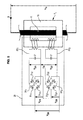
- Figure 1 shows a high-voltage transformer including a number N ⁇ 2 of elementary transformers T i .
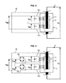
- Figures 2 and 3 show an elementary transformer T i according, respectively, to a first and a second embodiment.
- Each elementary transformer T i includes an elementary magnetic circuit 10, an elementary primary circuit 11, and an elementary secondary circuit 20.
- the elementary magnetic circuit 10 is intended to be coupled to the elementary primary circuit 11 and the elementary secondary circuit 20.
- Each elementary primary circuit 11 is supplied by an elementary primary voltage V1 i .
- the elementary primary circuits 11 are connected to one another in series so as to form a primary circuit 100 common to all of the elementary transformers T i .
- the common primary circuit 100 preferably consists of a winding of one turn for high-power applications or of two or more turns for low-power applications.
- the elementary magnetic circuits 10 of each elementary transformer T i are preferably toric and are arranged on the common circuit 100, which is preferably in the shape of a rectangular ring.
- Each elementary secondary circuit 20 includes at least one secondary winding 22 1 , 22 2 wound around the magnetic circuit 10.
- Each elementary secondary circuit 20 is intended to generate an elementary secondary voltage V20 i , which is balanced from one elementary transformer to another. In other words, the voltages generated by each elementary transformer are balanced with one another.
- the elementary secondary circuit 20 includes at least one capacitor C' with a known set value, each connected to the terminals of a secondary winding 22 1 , 22 2 .
- the magnetic circuits 11 can have dispersions, and the secondary voltages from one magnetic circuit to the other may not all be identical. These dispersions are due primarily to differences in permeability and cross-section. They are significant, typically more or less 30%, and it is expensive to remove them, for example by screening.
- a capacitor is preferred to a resistor (in order to obtain the same result) for minimizing losses.
- a resistor would add a dissipative element (which would generate losses) - an inductance (with a known set value) could also ensure the balancing function but would be complex (and expensive and bulky) to use.
- the voltage V at the output of the transformer is equal to the sum of the elementary balanced secondary voltages V20 i generated by the elementary secondary circuits 20.
- each elementary transformer T i generates the same voltage V2 i and it is the series arrangement of the elementary secondary circuits 20 that enables the high voltage V to be obtained at the outlet of the transformer.
- the total capacity at the terminals of the transformer decreases when the number N of elementary transformers increases.
- the transformer When the number N of elementary transformers is high, the transformer then has a low output capacity that enables it to switch very quickly from a first high voltage to a second high voltage. This performance is further enhanced when, in addition, the number of secondary windings is high, as the capacity at the terminals of each elementary transformer is itself decreased.
- the transformer can function so as to generate an alternating voltage (see figure 2 ).
- the transformer can function so as to generate a rectified voltage (see figure 3 ).
- each elementary transformer T i also includes a rectifier circuit 30 1 , 30 2 connected to the terminals of each winding of the elementary secondary circuit 20.
- Each rectifier circuit 30 1 , 30 2 is therefore mounted in parallel with the corresponding capacitor C'.
- the rectifier circuits 30 1 , 30 2 are also connected to one another.
- the elementary secondary circuits 20 are therefore connected to one another via these voltage rectifier circuits 30 1 , 30 2 .
- Such rectifier circuits 30 1 , 30 2 are, for example, known diode bridges (i.e. single rectifiers, doublers or multipliers).
- the output voltage of the transformer is equal to the sum of the elementary balanced secondary voltages from one transformer to the next and rectified, generated by each elementary transformer T i .
- Each elementary secondary circuit can include - as already mentioned - one or more windings.
- the elementary secondary circuit is therefore subdivided into a plurality of windings, enabling the alternating voltage to be reduced at the terminals of the balancing capacitors and at the terminals of the rectifiers.
- the generic components are in particular the capacitors and the elements of the rectifier circuits.
- the limitation of the voltage enables, in the case of rectified operation, the dielectric losses in the insulating material of the magnetic core windings to be limited (these losses are proportional to the square of the alternating voltage).
- the elementary secondary circuits include a plurality of secondary windings 22 1 , 22 2 , the latter are wound around the corresponding elementary magnetic circuit 10, alternating, with one in one direction and the other in the other direction.
- Such a method of winding the sections enables, by alternating the direction of the current in the windings, the maximum voltage between two adjacent windings to be reduced, facilitating the isolation between them.
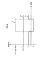
- the windings 22 1 and 22 2 have the same number of turns, and the voltages V21 i and V22 i are therefore equal; the maximum value of the voltage U A between alternating windings is then equal to half of the maximum value of the voltage U between non-alternating windings, which means a significant gain (see figure 6 ).
- each elementary transformer T i with two or more windings is identical to the voltage generated by an elementary transformer T i with one winding.
- the elementary transformers T i , the corresponding capacitors and the corresponding rectifier circuits are arranged in pairs on a printed circuit.
- the elementary transformers T i are positioned horizontally according to their main axis for static systems - transformer not subjected to accelerations - and tangentially for rotary systems - rotating transformer, subjected to centrifugal acceleration. This enables the cooling by convection of each elementary circuit to be significantly improved.
- the printed circuits including a pair of elementary transformers are then wound on the common primary circuit.
- the arrangement shown in figure 1 is obtained.
- the elementary magnetic circuits also consist of nanocrystalline iron. Such a material has good performance in terms of power density and magnetic coupling.
- this material Due to its high permeability, this material enables the number of turns of the primary winding 100 to be limited, and manages with a low-value balancing capacity, and is therefore less expensive and more compact.
- a filtration capacitor C f is added to the terminals of each rectifier 30 1 , 30 2 according to figure 7 .
- the transformer described above enables an X-ray tube to be supplied with power.
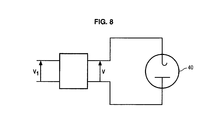
- the transformer connected to the X-ray tube 40 is shown in figure 8 .
Landscapes
- Engineering & Computer Science (AREA)
- Power Engineering (AREA)
- X-Ray Techniques (AREA)
Abstract
Description
- This invention relates generally to high-voltage transformers and more specifically those implemented in high-voltage power supplies, in particular those implemented in medical imaging devices and more specifically power supplies for X-ray tubes of such devices.
- There are numerous constraints on power supplies for X-ray tubes.
- These power supplies, when used, for example, in tomography, are in particular subjected to strong accelerations of several dozen G (the X-ray source rapidly rotating about the patient or the object to be imaged).
- In addition, these power supplies must be capable of switching very quickly from a first high voltage to a second high voltage so as to modify the nature of the X-rays, in order in particular to obtain a contrasted image of the patient or object.
- The components used in X-ray tube power supplies must be reliable and have good performances.
- In such a power supply, a limiting component is in particular the high-voltage transformer.
- Indeed, high-voltage transformers are complex in particular due to the high-voltage isolation between primary and secondary windings.
- In addition, the high-voltage transformer must satisfy mass and size constraints (it must be capable of being integrated in a medical imaging device) and be inexpensive.
- Various aspects of the invention enable a lightweight and compact high-voltage transformer to be obtained, implementing small magnetic circuits and integrating rectifier circuits consisting of generic components, therefore inexpensive and simple to produce by comparison with the known transformers.
- In addition, the transformer of the invention has superior performance over the known transformers.
- The transformer of one embodiment of the invention is based on the use of elementary transformers arranged on a common primary circuit and on the use of capacitors for balancing the voltages generated by the elementary secondary circuits of each elementary transformer.
- One aspect of the invention therefore relates to a high-voltage transformer including a plurality of elementary transformers.
- Each elementary transformer includes: an elementary primary circuit intended to be supplied by an elementary primary voltage and an elementary secondary circuit, in which each elementary secondary circuit includes at least one second winding; at least one capacitor, each connected to the terminals of a secondary winding so as to balance the secondary voltages with one another; in which the elementary secondary circuit is intended to generate a balanced elementary secondary voltage.
- Each elementary transformer also includes an elementary magnetic circuit intended to couple the elementary primary circuit and the elementary secondary circuit.
- The output voltage of such a transformer is equal to the sum of the balanced elementary secondary voltages, and the elementary primary circuits are connected to one another so as to form a common circuit with the elementary transformers, which common circuit is intended to be supplied by a primary voltage, in which the primary voltage is equal to the sum of the elementary primary voltages.
- The transformer can also optionally have one of the following features:
- each elementary transformer also includes at least one rectifier circuit, each connected to the terminals of a capacitor, in which the voltage at the output of the transformer is equal to the sum of the balanced and rectified elementary secondary voltages;
- in each elementary transformer, the secondary winding are alternately wound, one winding in one direction, the next in the other direction, so as to limit the voltage difference between two adjacent secondary windings wound around the elementary magnetic circuit;
- the magnetic circuits are made of nanocrystalline iron;
- each voltage rectifier circuit includes, at its terminals, a filtering capacitor, so as to generate a continuous voltage at the output of the transformer.
- According to a second aspect, the invention relates to a power supply for an X-ray tube including a high-voltage transformer according to the first aspect of the invention.
- According to a third aspect, the invention relates to a medical imaging device including a power supply for an X-ray tube according to the second aspect of the invention.
- Various features and advantages of the invention will become clear from the following description, provided solely for illustrative and non-limiting purposes, which should be read in reference to the appended drawings, in which:
-
figure 1 shows a high-voltage transformer according to an embodiment of the invention; -
figure 2 shows a first embodiment of an elementary transformer of the transformer according to an embodiment of the invention; -
figure 3 shows a second embodiment of an elementary transformer of the transformer according to an embodiment of the invention; -
figure 4 shows the elementary transformer of the second embodiment with windings in the same direction; -
figure 5 shows the elementary transformer of the second embodiment with alternating windings; -
figure 6 shows a timing chart of the voltages between two windings of an elementary transformer; -
figure 7 shows the transformer of the second embodiment in which the output voltage is rectified and filtered; -
figure 8 shows a high-voltage power supply connected to the X-ray tube. -
Figure 1 shows a high-voltage transformer including a number N≥2 of elementary transformers Ti. -
Figures 2 and 3 show an elementary transformer Ti according, respectively, to a first and a second embodiment. - Each elementary transformer Ti includes an elementary
magnetic circuit 10, an elementaryprimary circuit 11, and an elementarysecondary circuit 20. - For each elementary transformer Ti, the elementary
magnetic circuit 10 is intended to be coupled to the elementaryprimary circuit 11 and the elementarysecondary circuit 20. - Each elementary
primary circuit 11 is supplied by an elementary primary voltage V1i. - The elementary
primary circuits 11 are connected to one another in series so as to form aprimary circuit 100 common to all of the elementary transformers Ti. - The
common circuit 100 is supplied by a primary voltage Vi and each elementaryprimary circuit 11 is supplied - as already mentioned - by an elementary primary voltage V1i so that the primary voltage V1 is equal to the sum of the elementary primary voltages V1i is
- It is noted that the current I circulating in the elementary
primary circuits 11 is identical from one elementary transformer Ti to another. - The common
primary circuit 100 preferably consists of a winding of one turn for high-power applications or of two or more turns for low-power applications. - The elementary
magnetic circuits 10 of each elementary transformer Ti are preferably toric and are arranged on thecommon circuit 100, which is preferably in the shape of a rectangular ring. - Each elementary
secondary circuit 20 includes at least one secondary winding 221, 222 wound around themagnetic circuit 10. - Each elementary
secondary circuit 20 is intended to generate an elementary secondary voltage V20i, which is balanced from one elementary transformer to another. In other words, the voltages generated by each elementary transformer are balanced with one another. - To do this, the elementary
secondary circuit 20 includes at least one capacitor C' with a known set value, each connected to the terminals of a secondary winding 221, 222. - Indeed, the
magnetic circuits 11 can have dispersions, and the secondary voltages from one magnetic circuit to the other may not all be identical. These dispersions are due primarily to differences in permeability and cross-section. They are significant, typically more or less 30%, and it is expensive to remove them, for example by screening. - It should be noted that a capacitor is preferred to a resistor (in order to obtain the same result) for minimizing losses. Indeed, a resistor would add a dissipative element (which would generate losses) - an inductance (with a known set value) could also ensure the balancing function but would be complex (and expensive and bulky) to use.
- The voltage V at the output of the transformer is equal to the sum of the elementary balanced secondary voltages V20i generated by the elementary
secondary circuits 20. - Indeed, each elementary transformer Ti generates the same voltage V2i and it is the series arrangement of the elementary
secondary circuits 20 that enables the high voltage V to be obtained at the outlet of the transformer. - It should be noted that the total capacity at the terminals of the transformer, resulting from the association in series of the capacitors at the terminals of the N elementary transformers, decreases when the number N of elementary transformers increases. When the number N of elementary transformers is high, the transformer then has a low output capacity that enables it to switch very quickly from a first high voltage to a second high voltage. This performance is further enhanced when, in addition, the number of secondary windings is high, as the capacity at the terminals of each elementary transformer is itself decreased.
- According to a first embodiment, the transformer can function so as to generate an alternating voltage (see
figure 2 ). - According to a second embodiment, the transformer can function so as to generate a rectified voltage (see
figure 3 ). - In rectified operation, each elementary transformer Ti also includes a rectifier circuit 301, 302 connected to the terminals of each winding of the elementary
secondary circuit 20. - Each rectifier circuit 301, 302 is therefore mounted in parallel with the corresponding capacitor C'.
- The rectifier circuits 301, 302 are also connected to one another. The elementary
secondary circuits 20 are therefore connected to one another via these voltage rectifier circuits 301, 302. - Such rectifier circuits 301, 302 are, for example, known diode bridges (i.e. single rectifiers, doublers or multipliers).
- In the case of rectifier circuits, the output voltage of the transformer is equal to the sum of the elementary balanced secondary voltages from one transformer to the next and rectified, generated by each elementary transformer Ti.
- Each elementary secondary circuit can include - as already mentioned - one or more windings.
- The elementary secondary circuit is therefore subdivided into a plurality of windings, enabling the alternating voltage to be reduced at the terminals of the balancing capacitors and at the terminals of the rectifiers.
- This contributes to a reduction in the production costs and to an improvement in the reliability of the transformer, and enables high quantities of generic components to be implemented for numerous applications, and with proven technology (in particular 600V or 1200V capacitors and diodes).
- The generic components are in particular the capacitors and the elements of the rectifier circuits.
- For each elementary transformer Ti, these windings are distributed around the elementary
magnetic circuit 10. - The limitation of the voltage enables, in the case of rectified operation, the dielectric losses in the insulating material of the magnetic core windings to be limited (these losses are proportional to the square of the alternating voltage).
- If the elementary secondary circuits include a plurality of secondary windings 221, 222, the latter are wound around the corresponding elementary
magnetic circuit 10, alternating, with one in one direction and the other in the other direction. - Such a method of winding the sections enables, by alternating the direction of the current in the windings, the maximum voltage between two adjacent windings to be reduced, facilitating the isolation between them.
- In the case shown in
figure 4 , in which the secondary windings are all in the same direction, during the positive alternation of the voltage V11, the diodes D11, D13, D21 and D23 lead and the voltage U between the two windings 221 and 222 is zero; during the negative alternation of the voltage V1i, the diodes D12, D14, D22 and D24 lead and the voltage U between the two windings 221 and 222 is equal to the sum of the voltages V21i and V22i. - In the case shown in
figure 5 , in which the secondary windings are one in one direction and the other in the other directions, during the positive alternation of the voltage V1i, the diodes D11, D13, D22 and D24 lead and the voltage UA between the two windings 221 and 222 is equal to V22i; during the negative alternation of the voltage V1i, the diodes D12, D14, D21 and D23 lead and the voltage UA between the two windings 221 and 222 is equal to V21i. - In the most common embodiment, the windings 221 and 222 have the same number of turns, and the voltages V21i and V22i are therefore equal; the maximum value of the voltage UA between alternating windings is then equal to half of the maximum value of the voltage U between non-alternating windings, which means a significant gain (see
figure 6 ). - This result, described above for a single rectifier circuit, is also valid for a doubler-rectifier and for a multiplier-rectifier.
- It is noted that the voltage generated by each elementary transformer Ti with two or more windings is identical to the voltage generated by an elementary transformer Ti with one winding.
- In the production of the transformer, the elementary transformers Ti, the corresponding capacitors and the corresponding rectifier circuits are arranged in pairs on a printed circuit.
- The elementary transformers Ti are positioned horizontally according to their main axis for static systems - transformer not subjected to accelerations - and tangentially for rotary systems - rotating transformer, subjected to centrifugal acceleration. This enables the cooling by convection of each elementary circuit to be significantly improved.
- The printed circuits including a pair of elementary transformers are then wound on the common primary circuit. The arrangement shown in
figure 1 is obtained. - The elementary magnetic circuits also consist of nanocrystalline iron. Such a material has good performance in terms of power density and magnetic coupling.
- Due to its high permeability, this material enables the number of turns of the primary winding 100 to be limited, and manages with a low-value balancing capacity, and is therefore less expensive and more compact.
- Owing to the structure of the material, it is possible to operate at high frequencies with an acceptable level of losses.
- To generate a continuous voltage V at the output of the transformer, a filtration capacitor Cf is added to the terminals of each rectifier 301, 302 according to
figure 7 . - The transformer described above enables an X-ray tube to be supplied with power. The transformer connected to the
X-ray tube 40 is shown infigure 8 .
Claims (7)
- A high-voltage transformer including:-- a plurality of elementary transformers (Ti), in which each elementary transformer (Ti) includes-- an elementary primary circuit (11) intended to be powered by an elementary primary voltage (V1i);-- an elementary secondary circuit (20) includingin which the elementary secondary circuit (20) is intended to generate an elementary balanced secondary voltage (V20i)--- at least one secondary winding (221, 222);--- at least one capacitor (C'), each connected to the terminals of a secondary winding (221, 222) so as to balance the secondary voltages (V21i, V22i) with one another;-- an elementary magnetic circuit (10) intended to couple the elementary primary circuit (11) and the elementary secondary circuit (20);in which the output voltage (V) of the transformer is equal to the sum of the elementary balanced secondary voltages (V20i), and the elementary primary circuits (11) are connected to one another so as to form a common circuit (100) with the elementary transformers (Ti), in which said common circuit (100) is intended to be supplied by a primary voltage (V1), which primary voltage (VI) is equal to the sum of the elementary primary voltages (V1i).
- The transformer according to claim 1, in which each elementary transformer also includes at least one voltage rectifier circuit (301, 302), each connected to the terminals of a capacitor (C'), in which the output voltage (V) of the transformer is equal to the sum of the balanced and rectified elementary secondary voltages.
- The transformer according to any preceding claim, in which, in each elementary transformer (Ti), the secondary windings are alternately wound, one winding in one direction, the next in the other direction, so as to limit the voltage difference between two adjacent secondary windings wound around the elementary magnetic circuit (10).
- The transformer according to any one of the previous claims, in which the magnetic circuits are made of nanocrystalline iron.
- The transformer according to any one of claims 2 to 4 in which each voltage rectifier circuit (301, 302) includes, at its terminals, a filtering capacitor (Cf), so as to generate a continuous voltage (V) at the outlet of the transformer.
- A power supply for an X-ray tube including a high-voltage transformer according to any preceding claim.
- A medical imaging device including an X-ray tube power supply according to claim 6.
Applications Claiming Priority (1)
| Application Number | Priority Date | Filing Date | Title |
|---|---|---|---|
| FR0951945A FR2943837B1 (en) | 2009-03-25 | 2009-03-25 | HIGH VOLTAGE TRANSFORMER AND POWER SUPPLY OF AN X-RAY TUBE COMPRISING SUCH A TRANSFORMER |
Publications (3)
| Publication Number | Publication Date |
|---|---|
| EP2234127A2 true EP2234127A2 (en) | 2010-09-29 |
| EP2234127A3 EP2234127A3 (en) | 2010-12-08 |
| EP2234127B1 EP2234127B1 (en) | 2013-06-05 |
Family
ID=41723020
Family Applications (1)
| Application Number | Title | Priority Date | Filing Date |
|---|---|---|---|
| EP10156618.0A Active EP2234127B1 (en) | 2009-03-25 | 2010-03-16 | High-voltage transformer and power supply |
Country Status (4)
| Country | Link |
|---|---|
| US (1) | US8098124B2 (en) |
| EP (1) | EP2234127B1 (en) |
| CN (1) | CN101860224B (en) |
| FR (1) | FR2943837B1 (en) |
Families Citing this family (1)
| Publication number | Priority date | Publication date | Assignee | Title |
|---|---|---|---|---|
| US10700551B2 (en) | 2018-05-21 | 2020-06-30 | Raytheon Company | Inductive wireless power transfer device with improved coupling factor and high voltage isolation |
Family Cites Families (15)
| Publication number | Priority date | Publication date | Assignee | Title |
|---|---|---|---|---|
| US3263151A (en) * | 1962-07-02 | 1966-07-26 | Gen Electric | Power supply for x-ray apparatus |
| US3281643A (en) * | 1962-07-02 | 1966-10-25 | Gen Electric | X-ray resonant transformer power supply |
| US3502877A (en) * | 1967-07-07 | 1970-03-24 | Picker Corp | Grid-controlled x-ray tube control system |
| FR2239040A1 (en) * | 1973-07-26 | 1975-02-21 | Pierson Gerald | HV d.c. generator for electrostatic painting - has series of bridge rectifiers connected to secondary windings |
| FR2643534B1 (en) * | 1989-02-02 | 1993-09-17 | Gen Electric Cgr | HIGH VOLTAGE SUPPLY DEVICE FOR X-RAY TUBE |
| US5023768A (en) * | 1989-11-24 | 1991-06-11 | Varian Associates, Inc. | High voltage high power DC power supply |
| DE69019310T2 (en) * | 1989-11-24 | 1995-09-21 | Varian Associates | Power supply device with high DC voltage and high power. |
| DE4107199C2 (en) * | 1991-03-06 | 1994-12-08 | Siemens Ag | High frequency x-ray generator |
| US5335161A (en) * | 1992-03-30 | 1994-08-02 | Lorad Corporation | High voltage multipliers and filament transformers for portable X-ray inspection units |
| US5757633A (en) * | 1995-12-04 | 1998-05-26 | General Atomics | High efficiency multistep sinewave synthesizer |
| US5835367A (en) * | 1998-01-20 | 1998-11-10 | Industrial Technology Research Institute | Distributed plannar-type high voltage transformer |
| US6900557B1 (en) * | 2000-01-10 | 2005-05-31 | Diversified Technologies, Inc. | High power modulator |
| DE10048146A1 (en) * | 2000-09-28 | 2002-04-11 | Philips Corp Intellectual Pty | Power supply for X-ray generator |
| DE10218456A1 (en) * | 2002-04-25 | 2003-11-06 | Abb Patent Gmbh | Switching power supply arrangement |
| DE102006040026B4 (en) * | 2006-08-25 | 2015-06-18 | Minebea Co., Ltd. | Transformer for current balancing |
-
2009
- 2009-03-25 FR FR0951945A patent/FR2943837B1/en active Active
-
2010
- 2010-03-16 EP EP10156618.0A patent/EP2234127B1/en active Active
- 2010-03-25 US US12/731,176 patent/US8098124B2/en active Active
- 2010-03-25 CN CN201010159593.8A patent/CN101860224B/en active Active
Non-Patent Citations (1)
| Title |
|---|
| None |
Also Published As
| Publication number | Publication date |
|---|---|
| FR2943837B1 (en) | 2015-07-03 |
| EP2234127A3 (en) | 2010-12-08 |
| CN101860224B (en) | 2015-01-28 |
| CN101860224A (en) | 2010-10-13 |
| EP2234127B1 (en) | 2013-06-05 |
| US20100245014A1 (en) | 2010-09-30 |
| US8098124B2 (en) | 2012-01-17 |
| FR2943837A1 (en) | 2010-10-01 |
Similar Documents
| Publication | Publication Date | Title |
|---|---|---|
| CN111902895B (en) | Shielded power transformer | |
| CN106877685B (en) | AC/DC power conversion system and its manufacturing method | |
| US7332992B2 (en) | Transformer | |
| US20100301985A1 (en) | High-voltage power generation system and package | |
| EP2194545A2 (en) | Transformer with high voltage isolation | |
| US20090257560A1 (en) | 3d poly-phase transformer | |
| JP2024119944A (en) | Apparatus and method with power conversion using multiple rectifier circuits | |
| US9369060B2 (en) | Power generation system and package | |
| JP2016058495A (en) | Common mode choke coil, common mode filter, and power converter | |
| US3596167A (en) | Cascade transformer high voltage generator | |
| US6982884B1 (en) | Autotransformers to parallel AC to DC converters | |
| EP2234127B1 (en) | High-voltage transformer and power supply | |
| EP3214628A2 (en) | Line-frequency rotary transformer for computed tomography gantry | |
| US4443843A (en) | DC High voltage generator for a dental X-ray photographing apparatus | |
| US3539903A (en) | Cascade rectifier voltage multiplier with resonance coil | |
| SE447527B (en) | HIGH FREQUENCY FERROR RESONANCE ENERGY FOR A DEVICING AND HIGH VOLTAGE CIRCUIT IN A TV RECEIVER | |
| US9160248B2 (en) | Voltage multiplier | |
| KR101463388B1 (en) | Bidirectional semiconductor transformer using voltage doubler circuit structure | |
| JPH0350508B2 (en) | ||
| US10312881B2 (en) | Filters for adjustable speed drives with low DC bus capacitance and methods of manufacture and use thereof | |
| US20160262250A1 (en) | Power generation system and package | |
| CN110036558A (en) | Small charger for electrical equipment | |
| JP2518471B2 (en) | Multi-stage insulation transformer type high voltage generator | |
| JPH0710175B2 (en) | Multi-stage insulation transformer type high voltage generator | |
| CN110364332A (en) | Polyphase transformer |
Legal Events
| Date | Code | Title | Description |
|---|---|---|---|
| PUAI | Public reference made under article 153(3) epc to a published international application that has entered the european phase |
Free format text: ORIGINAL CODE: 0009012 |
|
| AK | Designated contracting states |
Kind code of ref document: A2 Designated state(s): AT BE BG CH CY CZ DE DK EE ES FI FR GB GR HR HU IE IS IT LI LT LU LV MC MK MT NL NO PL PT RO SE SI SK SM TR |
|
| AX | Request for extension of the european patent |
Extension state: AL BA ME RS |
|
| PUAL | Search report despatched |
Free format text: ORIGINAL CODE: 0009013 |
|
| AK | Designated contracting states |
Kind code of ref document: A3 Designated state(s): AT BE BG CH CY CZ DE DK EE ES FI FR GB GR HR HU IE IS IT LI LT LU LV MC MK MT NL NO PL PT RO SE SI SK SM TR |
|
| AX | Request for extension of the european patent |
Extension state: AL BA ME RS |
|
| 17P | Request for examination filed |
Effective date: 20110608 |
|
| GRAP | Despatch of communication of intention to grant a patent |
Free format text: ORIGINAL CODE: EPIDOSNIGR1 |
|
| GRAS | Grant fee paid |
Free format text: ORIGINAL CODE: EPIDOSNIGR3 |
|
| GRAA | (expected) grant |
Free format text: ORIGINAL CODE: 0009210 |
|
| AK | Designated contracting states |
Kind code of ref document: B1 Designated state(s): AT BE BG CH CY CZ DE DK EE ES FI FR GB GR HR HU IE IS IT LI LT LU LV MC MK MT NL NO PL PT RO SE SI SK SM TR |
|
| REG | Reference to a national code |
Ref country code: GB Ref legal event code: FG4D |
|
| REG | Reference to a national code |
Ref country code: CH Ref legal event code: EP |
|
| REG | Reference to a national code |
Ref country code: AT Ref legal event code: REF Ref document number: 616084 Country of ref document: AT Kind code of ref document: T Effective date: 20130615 |
|
| REG | Reference to a national code |
Ref country code: IE Ref legal event code: FG4D |
|
| REG | Reference to a national code |
Ref country code: DE Ref legal event code: R096 Ref document number: 602010007480 Country of ref document: DE Effective date: 20130801 |
|
| REG | Reference to a national code |
Ref country code: AT Ref legal event code: MK05 Ref document number: 616084 Country of ref document: AT Kind code of ref document: T Effective date: 20130605 |
|
| PG25 | Lapsed in a contracting state [announced via postgrant information from national office to epo] |
Ref country code: ES Free format text: LAPSE BECAUSE OF FAILURE TO SUBMIT A TRANSLATION OF THE DESCRIPTION OR TO PAY THE FEE WITHIN THE PRESCRIBED TIME-LIMIT Effective date: 20130916 Ref country code: SI Free format text: LAPSE BECAUSE OF FAILURE TO SUBMIT A TRANSLATION OF THE DESCRIPTION OR TO PAY THE FEE WITHIN THE PRESCRIBED TIME-LIMIT Effective date: 20130605 Ref country code: LT Free format text: LAPSE BECAUSE OF FAILURE TO SUBMIT A TRANSLATION OF THE DESCRIPTION OR TO PAY THE FEE WITHIN THE PRESCRIBED TIME-LIMIT Effective date: 20130605 Ref country code: GR Free format text: LAPSE BECAUSE OF FAILURE TO SUBMIT A TRANSLATION OF THE DESCRIPTION OR TO PAY THE FEE WITHIN THE PRESCRIBED TIME-LIMIT Effective date: 20130906 Ref country code: NO Free format text: LAPSE BECAUSE OF FAILURE TO SUBMIT A TRANSLATION OF THE DESCRIPTION OR TO PAY THE FEE WITHIN THE PRESCRIBED TIME-LIMIT Effective date: 20130905 Ref country code: FI Free format text: LAPSE BECAUSE OF FAILURE TO SUBMIT A TRANSLATION OF THE DESCRIPTION OR TO PAY THE FEE WITHIN THE PRESCRIBED TIME-LIMIT Effective date: 20130605 Ref country code: SE Free format text: LAPSE BECAUSE OF FAILURE TO SUBMIT A TRANSLATION OF THE DESCRIPTION OR TO PAY THE FEE WITHIN THE PRESCRIBED TIME-LIMIT Effective date: 20130605 Ref country code: AT Free format text: LAPSE BECAUSE OF FAILURE TO SUBMIT A TRANSLATION OF THE DESCRIPTION OR TO PAY THE FEE WITHIN THE PRESCRIBED TIME-LIMIT Effective date: 20130605 |
|
| REG | Reference to a national code |
Ref country code: NL Ref legal event code: VDEP Effective date: 20130605 |
|
| REG | Reference to a national code |
Ref country code: LT Ref legal event code: MG4D |
|
| PG25 | Lapsed in a contracting state [announced via postgrant information from national office to epo] |
Ref country code: HR Free format text: LAPSE BECAUSE OF FAILURE TO SUBMIT A TRANSLATION OF THE DESCRIPTION OR TO PAY THE FEE WITHIN THE PRESCRIBED TIME-LIMIT Effective date: 20130605 Ref country code: BG Free format text: LAPSE BECAUSE OF FAILURE TO SUBMIT A TRANSLATION OF THE DESCRIPTION OR TO PAY THE FEE WITHIN THE PRESCRIBED TIME-LIMIT Effective date: 20130905 |
|
| PG25 | Lapsed in a contracting state [announced via postgrant information from national office to epo] |
Ref country code: LV Free format text: LAPSE BECAUSE OF FAILURE TO SUBMIT A TRANSLATION OF THE DESCRIPTION OR TO PAY THE FEE WITHIN THE PRESCRIBED TIME-LIMIT Effective date: 20130605 |
|
| PG25 | Lapsed in a contracting state [announced via postgrant information from national office to epo] |
Ref country code: CZ Free format text: LAPSE BECAUSE OF FAILURE TO SUBMIT A TRANSLATION OF THE DESCRIPTION OR TO PAY THE FEE WITHIN THE PRESCRIBED TIME-LIMIT Effective date: 20130605 Ref country code: EE Free format text: LAPSE BECAUSE OF FAILURE TO SUBMIT A TRANSLATION OF THE DESCRIPTION OR TO PAY THE FEE WITHIN THE PRESCRIBED TIME-LIMIT Effective date: 20130605 Ref country code: PT Free format text: LAPSE BECAUSE OF FAILURE TO SUBMIT A TRANSLATION OF THE DESCRIPTION OR TO PAY THE FEE WITHIN THE PRESCRIBED TIME-LIMIT Effective date: 20131007 Ref country code: BE Free format text: LAPSE BECAUSE OF FAILURE TO SUBMIT A TRANSLATION OF THE DESCRIPTION OR TO PAY THE FEE WITHIN THE PRESCRIBED TIME-LIMIT Effective date: 20130605 Ref country code: IS Free format text: LAPSE BECAUSE OF FAILURE TO SUBMIT A TRANSLATION OF THE DESCRIPTION OR TO PAY THE FEE WITHIN THE PRESCRIBED TIME-LIMIT Effective date: 20131005 Ref country code: SK Free format text: LAPSE BECAUSE OF FAILURE TO SUBMIT A TRANSLATION OF THE DESCRIPTION OR TO PAY THE FEE WITHIN THE PRESCRIBED TIME-LIMIT Effective date: 20130605 |
|
| PG25 | Lapsed in a contracting state [announced via postgrant information from national office to epo] |
Ref country code: PL Free format text: LAPSE BECAUSE OF FAILURE TO SUBMIT A TRANSLATION OF THE DESCRIPTION OR TO PAY THE FEE WITHIN THE PRESCRIBED TIME-LIMIT Effective date: 20130605 Ref country code: NL Free format text: LAPSE BECAUSE OF FAILURE TO SUBMIT A TRANSLATION OF THE DESCRIPTION OR TO PAY THE FEE WITHIN THE PRESCRIBED TIME-LIMIT Effective date: 20130605 Ref country code: RO Free format text: LAPSE BECAUSE OF FAILURE TO SUBMIT A TRANSLATION OF THE DESCRIPTION OR TO PAY THE FEE WITHIN THE PRESCRIBED TIME-LIMIT Effective date: 20130605 |
|
| PLBE | No opposition filed within time limit |
Free format text: ORIGINAL CODE: 0009261 |
|
| STAA | Information on the status of an ep patent application or granted ep patent |
Free format text: STATUS: NO OPPOSITION FILED WITHIN TIME LIMIT |
|
| PG25 | Lapsed in a contracting state [announced via postgrant information from national office to epo] |
Ref country code: DK Free format text: LAPSE BECAUSE OF FAILURE TO SUBMIT A TRANSLATION OF THE DESCRIPTION OR TO PAY THE FEE WITHIN THE PRESCRIBED TIME-LIMIT Effective date: 20130605 |
|
| 26N | No opposition filed |
Effective date: 20140306 |
|
| PG25 | Lapsed in a contracting state [announced via postgrant information from national office to epo] |
Ref country code: IT Free format text: LAPSE BECAUSE OF FAILURE TO SUBMIT A TRANSLATION OF THE DESCRIPTION OR TO PAY THE FEE WITHIN THE PRESCRIBED TIME-LIMIT Effective date: 20130605 |
|
| REG | Reference to a national code |
Ref country code: DE Ref legal event code: R097 Ref document number: 602010007480 Country of ref document: DE Effective date: 20140306 |
|
| PG25 | Lapsed in a contracting state [announced via postgrant information from national office to epo] |
Ref country code: LU Free format text: LAPSE BECAUSE OF FAILURE TO SUBMIT A TRANSLATION OF THE DESCRIPTION OR TO PAY THE FEE WITHIN THE PRESCRIBED TIME-LIMIT Effective date: 20140316 |
|
| REG | Reference to a national code |
Ref country code: CH Ref legal event code: PL |
|
| GBPC | Gb: european patent ceased through non-payment of renewal fee |
Effective date: 20140316 |
|
| REG | Reference to a national code |
Ref country code: FR Ref legal event code: ST Effective date: 20141128 |
|
| REG | Reference to a national code |
Ref country code: IE Ref legal event code: MM4A |
|
| PG25 | Lapsed in a contracting state [announced via postgrant information from national office to epo] |
Ref country code: CH Free format text: LAPSE BECAUSE OF NON-PAYMENT OF DUE FEES Effective date: 20140331 Ref country code: GB Free format text: LAPSE BECAUSE OF NON-PAYMENT OF DUE FEES Effective date: 20140316 Ref country code: FR Free format text: LAPSE BECAUSE OF NON-PAYMENT OF DUE FEES Effective date: 20140331 Ref country code: LI Free format text: LAPSE BECAUSE OF NON-PAYMENT OF DUE FEES Effective date: 20140331 Ref country code: IE Free format text: LAPSE BECAUSE OF NON-PAYMENT OF DUE FEES Effective date: 20140316 |
|
| PG25 | Lapsed in a contracting state [announced via postgrant information from national office to epo] |
Ref country code: MT Free format text: LAPSE BECAUSE OF FAILURE TO SUBMIT A TRANSLATION OF THE DESCRIPTION OR TO PAY THE FEE WITHIN THE PRESCRIBED TIME-LIMIT Effective date: 20130605 |
|
| PG25 | Lapsed in a contracting state [announced via postgrant information from national office to epo] |
Ref country code: SM Free format text: LAPSE BECAUSE OF FAILURE TO SUBMIT A TRANSLATION OF THE DESCRIPTION OR TO PAY THE FEE WITHIN THE PRESCRIBED TIME-LIMIT Effective date: 20130605 |
|
| PG25 | Lapsed in a contracting state [announced via postgrant information from national office to epo] |
Ref country code: MC Free format text: LAPSE BECAUSE OF FAILURE TO SUBMIT A TRANSLATION OF THE DESCRIPTION OR TO PAY THE FEE WITHIN THE PRESCRIBED TIME-LIMIT Effective date: 20130605 |
|
| PG25 | Lapsed in a contracting state [announced via postgrant information from national office to epo] |
Ref country code: CY Free format text: LAPSE BECAUSE OF FAILURE TO SUBMIT A TRANSLATION OF THE DESCRIPTION OR TO PAY THE FEE WITHIN THE PRESCRIBED TIME-LIMIT Effective date: 20130605 |
|
| PG25 | Lapsed in a contracting state [announced via postgrant information from national office to epo] |
Ref country code: TR Free format text: LAPSE BECAUSE OF FAILURE TO SUBMIT A TRANSLATION OF THE DESCRIPTION OR TO PAY THE FEE WITHIN THE PRESCRIBED TIME-LIMIT Effective date: 20130605 Ref country code: HU Free format text: LAPSE BECAUSE OF FAILURE TO SUBMIT A TRANSLATION OF THE DESCRIPTION OR TO PAY THE FEE WITHIN THE PRESCRIBED TIME-LIMIT; INVALID AB INITIO Effective date: 20100316 |
|
| PG25 | Lapsed in a contracting state [announced via postgrant information from national office to epo] |
Ref country code: MK Free format text: LAPSE BECAUSE OF FAILURE TO SUBMIT A TRANSLATION OF THE DESCRIPTION OR TO PAY THE FEE WITHIN THE PRESCRIBED TIME-LIMIT Effective date: 20130605 |
|
| P01 | Opt-out of the competence of the unified patent court (upc) registered |
Effective date: 20230528 |
|
| REG | Reference to a national code |
Ref country code: DE Ref legal event code: R081 Ref document number: 602010007480 Country of ref document: DE Owner name: GE PRECISION HEALTHCARE LLC, WAUKESHA, US Free format text: FORMER OWNER: GENERAL ELECTRIC COMPANY, SCHENECTADY, NY, US |
|
| PGFP | Annual fee paid to national office [announced via postgrant information from national office to epo] |
Ref country code: DE Payment date: 20260219 Year of fee payment: 17 |