EP2231507B1 - A method for making a 3d nanostructure having a nanosubstructure, such as an insulating pyramid having a metallic tip - Google Patents
A method for making a 3d nanostructure having a nanosubstructure, such as an insulating pyramid having a metallic tip Download PDFInfo
- Publication number
- EP2231507B1 EP2231507B1 EP08869344.5A EP08869344A EP2231507B1 EP 2231507 B1 EP2231507 B1 EP 2231507B1 EP 08869344 A EP08869344 A EP 08869344A EP 2231507 B1 EP2231507 B1 EP 2231507B1
- Authority
- EP
- European Patent Office
- Prior art keywords
- mold
- silicon
- structural material
- pyramid
- nanosubstructure
- Prior art date
- Legal status (The legal status is an assumption and is not a legal conclusion. Google has not performed a legal analysis and makes no representation as to the accuracy of the status listed.)
- Active
Links
Images






Classifications
-
- B—PERFORMING OPERATIONS; TRANSPORTING
- B81—MICROSTRUCTURAL TECHNOLOGY
- B81C—PROCESSES OR APPARATUS SPECIALLY ADAPTED FOR THE MANUFACTURE OR TREATMENT OF MICROSTRUCTURAL DEVICES OR SYSTEMS
- B81C1/00—Manufacture or treatment of devices or systems in or on a substrate
- B81C1/00015—Manufacture or treatment of devices or systems in or on a substrate for manufacturing microsystems
- B81C1/00023—Manufacture or treatment of devices or systems in or on a substrate for manufacturing microsystems without movable or flexible elements
- B81C1/00111—Tips, pillars, i.e. raised structures
-
- B—PERFORMING OPERATIONS; TRANSPORTING
- B82—NANOTECHNOLOGY
- B82Y—SPECIFIC USES OR APPLICATIONS OF NANOSTRUCTURES; MEASUREMENT OR ANALYSIS OF NANOSTRUCTURES; MANUFACTURE OR TREATMENT OF NANOSTRUCTURES
- B82Y35/00—Methods or apparatus for measurement or analysis of nanostructures
-
- G—PHYSICS
- G01—MEASURING; TESTING
- G01Q—SCANNING-PROBE TECHNIQUES OR APPARATUS; APPLICATIONS OF SCANNING-PROBE TECHNIQUES, e.g. SCANNING PROBE MICROSCOPY [SPM]
- G01Q70/00—General aspects of SPM probes, their manufacture or their related instrumentation, insofar as they are not specially adapted to a single SPM technique covered by group G01Q60/00
- G01Q70/08—Probe characteristics
- G01Q70/10—Shape or taper
-
- G—PHYSICS
- G01—MEASURING; TESTING
- G01Q—SCANNING-PROBE TECHNIQUES OR APPARATUS; APPLICATIONS OF SCANNING-PROBE TECHNIQUES, e.g. SCANNING PROBE MICROSCOPY [SPM]
- G01Q70/00—General aspects of SPM probes, their manufacture or their related instrumentation, insofar as they are not specially adapted to a single SPM technique covered by group G01Q60/00
- G01Q70/16—Probe manufacture
-
- B—PERFORMING OPERATIONS; TRANSPORTING
- B33—ADDITIVE MANUFACTURING TECHNOLOGY
- B33Y—ADDITIVE MANUFACTURING, i.e. MANUFACTURING OF THREE-DIMENSIONAL [3D] OBJECTS BY ADDITIVE DEPOSITION, ADDITIVE AGGLOMERATION OR ADDITIVE LAYERING, e.g. BY 3D PRINTING, STEREOLITHOGRAPHY OR SELECTIVE LASER SINTERING
- B33Y10/00—Processes of additive manufacturing
-
- B—PERFORMING OPERATIONS; TRANSPORTING
- B33—ADDITIVE MANUFACTURING TECHNOLOGY
- B33Y—ADDITIVE MANUFACTURING, i.e. MANUFACTURING OF THREE-DIMENSIONAL [3D] OBJECTS BY ADDITIVE DEPOSITION, ADDITIVE AGGLOMERATION OR ADDITIVE LAYERING, e.g. BY 3D PRINTING, STEREOLITHOGRAPHY OR SELECTIVE LASER SINTERING
- B33Y80/00—Products made by additive manufacturing
-
- B—PERFORMING OPERATIONS; TRANSPORTING
- B81—MICROSTRUCTURAL TECHNOLOGY
- B81C—PROCESSES OR APPARATUS SPECIALLY ADAPTED FOR THE MANUFACTURE OR TREATMENT OF MICROSTRUCTURAL DEVICES OR SYSTEMS
- B81C2201/00—Manufacture or treatment of microstructural devices or systems
- B81C2201/03—Processes for manufacturing substrate-free structures
- B81C2201/034—Moulding
-
- Y—GENERAL TAGGING OF NEW TECHNOLOGICAL DEVELOPMENTS; GENERAL TAGGING OF CROSS-SECTIONAL TECHNOLOGIES SPANNING OVER SEVERAL SECTIONS OF THE IPC; TECHNICAL SUBJECTS COVERED BY FORMER USPC CROSS-REFERENCE ART COLLECTIONS [XRACs] AND DIGESTS
- Y10—TECHNICAL SUBJECTS COVERED BY FORMER USPC
- Y10T—TECHNICAL SUBJECTS COVERED BY FORMER US CLASSIFICATION
- Y10T428/00—Stock material or miscellaneous articles
- Y10T428/29—Coated or structually defined flake, particle, cell, strand, strand portion, rod, filament, macroscopic fiber or mass thereof
- Y10T428/2913—Rod, strand, filament or fiber
-
- Y—GENERAL TAGGING OF NEW TECHNOLOGICAL DEVELOPMENTS; GENERAL TAGGING OF CROSS-SECTIONAL TECHNOLOGIES SPANNING OVER SEVERAL SECTIONS OF THE IPC; TECHNICAL SUBJECTS COVERED BY FORMER USPC CROSS-REFERENCE ART COLLECTIONS [XRACs] AND DIGESTS
- Y10—TECHNICAL SUBJECTS COVERED BY FORMER USPC
- Y10T—TECHNICAL SUBJECTS COVERED BY FORMER US CLASSIFICATION
- Y10T428/00—Stock material or miscellaneous articles
- Y10T428/29—Coated or structually defined flake, particle, cell, strand, strand portion, rod, filament, macroscopic fiber or mass thereof
- Y10T428/2982—Particulate matter [e.g., sphere, flake, etc.]
Definitions
- the present invention relates to a method for making a 3D nanostructure having a nanosubstructure, such as an insulating pyramid having a metallic tip.
- nanotechnology means that the relevant dimension is less than 100nm. This implies that the 3D nanostructure and substructures may be typically a few microns large, but would be much smaller.
- nano also encompasses structure with a relevant dimension up to 100 microns, preferably up to 50 microns or up to 10 microns. The lower limit is about 1nm, preferably about 5 or 10nm.
- Another fabrication strategy includes the use of stress induced retardation of oxide growth in corners to create nano-apertures (See A. Vollkopf, O. Rudow, M. Muller-Wiegand, G. Georgiev, E. Oesterschulze, "Influence of the oxidation temperature on the fabrication process of silicon dioxide aperture tips", Appl. Phys. A, 76 (2003), p. 923-926 ),and low temperature oxidation and selective etching (LOSE) to create an aperture at the apex of a pyramidal tip (see P.N. Minh, T. Ono, and M. Esashi, "Non-uniform silicon oxidation and application for the fabrication of aperture for near-field scanning optical microscopy", Appl. Phys. Lett., 75 (1999), pp. 4076-4078 .
- LOSE low temperature oxidation and selective etching
- stringers a thickness of the corners
- stringers t / sin ⁇ / 2 ⁇ R
- corner lithography either constitute the structural material of wire structures and tips, or are used as a masking material in subsequent fabrication steps.
- the general fabrication method consists of a few basic steps: (1) mold fabrication, (2) conformal deposition of the structural material, (3) isotropic thinning of the structural layer, nanowires remain in sharp concave corners and (4) removal of the mold.
- the present invention has for its object to provide a method for making 3D nanostructures having at least one nanosubstructure.
- the invention is based on the insight that by using corner lithography it is possible to create such nanosubstructures and nanowires without the need of nano lithography.
- structural material that remains after conformal deposition and subsequent isotropic thinning of a thin film in sharp concave corners is used as a mask. From the embodiment given it is clear that several steps are added, to create an inversion mask.
- the method according to an example is a powerful technique for nano-patterning of pyramidal tips, as the ones used in scanning probe microscopy (SPM).
- pyramids provided with apertures can be used for liquid meniscus manipulation.
- the 3D oriented wires can be used for manipulating a liquid droplet.
- these nanowires can be used for advanced measurements whereas effects typical for nanowires can now be determined in a 3D mode.
- 3D fluidum (gas/liquid) channels can be made (see for 2D fluidum channels: N.R. Tas, J.W. Berenschot, P. Mela, H.V. Jansen, M. Elwenspoek, A..van den Berg, "2D-Confined Nanochannels Fabricated by Conventional Micromachining", Nano Lett., 2 (2002), pp. 1031-1032 .
- the present invention provides a method for making a 3D nanostructure having a nanosubstructure according to claim 1, comprising the steps of: i) providing a mold comprising at least one sharp concave corner; ii) conformal depositing at least one structural material in at least the sharp concave corner; iii) isotropically removing structural material; iv) depositing at least one other structural material; v) removing earlier deposited structural material; vi) forming a nanosubstructure; and vii) removing the mold thereby providing the 3D nanostructure having the nanosubstructure.
- a sharp concave corner has an angle which in principle is greater than 0° and less than 180°. More practically the angles lies between about 10° and about 170°.
- the crystal angles are at about 70°, 90° en 110°. Using other crystal structures for the mold will allow the use of different angles.
- an important (silicon) etching method for micromachining is the so called deep reactive ion etching (DRIE). DRIE etches substancially perpendicular to the (silicon) substrate. This implies that the angle will be in a range around 90°. Furhtermore, at angles close to 180° the differential overetching for selctively removing material will be more difficult. Thus, the angles could be within the range of 30° to 150°, such as 50° to 140°, or from 60° to 120°.
- the 3D nanostructure has a pyramidal form and the conformal deposition takes place in at least the pyramidal apex and/or rigdes.
- the conformal deposition takes place in at least the pyramidal apex and/or rigdes.
- other 3D structures such as cones and pyramids with a triangular or multigonal base, are also possible.
- the structural material can be used as the structural material.
- Examples are polysilicon, silicon nitride and silicon oxide.
- Preferred are materials that can be conformally deposited using different methods and can be (isotropically) removed by different methods using conditions which are not negatively effecting the other applied materials.
- the other structural material deposited by local oxidation of the silicon mold and/or oxidation of a previously deposited structural material, such as poly silicon.
- the step vi) of forming the nanosubstructure may comprise a further material deposition, such as metal, plastic, porous material or mixtures thereof. More preferably the metal deposition results in the formation of an insulating pyramid having a metallic tip.
- Such metallic tip can be used as catalyst for e.g. carbon nanotube (- nanofiber) growth,as a local electrode for electrical or electrochemical measurement + stimulus, or for surface enhanced raman spectroscopy (SERS) measurements.
- the single hole at the apex can be used as a dopingmask.
- Mono crystalline silicon or poly-Silicon
- boron doped p++ silicon nano-dot or line
- Such structure conducts electricity well.
- this layer may be maintained when the mold is removed by etching. This results in the formation of a p++ nanodot or line.
- a metal contact can be provided to the top surface.
- TMAH Low Pressure Chemical Vapour Deposited, LPCVD
- silicon oxide thermal
- LPCVD low stress silicon nitride
- Table 1 summarizes the etch rates of these materials in the etchants used in the examples.
- TMAH refers to a 5 wt% solution of tetramethyl ammonium hydroxide in water at 70 °C. 50% HF etching. is performed at room temperature, without stirring.
- H 3 PO 4 refers to a 85 vol% solution at 180°C.
- Fig. 1 shows the fabrication scheme for an oxide pyramid supporting a nanosubstruture metal tip. Fabrication started with the mold fabrication, in this case by KOH etching in a ⁇ 100> silicon wafer to create the pyramidal hole bounded by the ⁇ 111> planes. Next, silicon nitride (220 nm) was deposited by LPCVD (conformal deposition) and isotropically removed in 50% HF (84 min. at room temperature).
- This is a timed etch step which required a 1.23 times over-etching to remove the silicon nitride in the four oblique ribs of the pyramidal hole ( ⁇ 109.4°) and leaving only a small piece of silicon nitride at the tip.
- a dummy wafer containing the same thickness of silicon nitride was etched in parallel.
- the silicon oxide structural material for the pyramid was formed by local oxidation of the silicon (LOCOS) (see J.A. Appels, E. Kooi, M.M. Paffen, J.J. H. Schatorje, W. Verkuylen, "Local oxidation of silicon and its applications in semiconductor-device technology", Philips Res.
- LOC local oxidation of the silicon
- TMAH is a suitable etchant for this step as it has a high selectivity for silicon as compared to silicon oxide (table 1) [7].
- Fig. 2 shows the fabricated silicon oxide pyramid having a Chromium tip of less than 300 nm in size.
- the pyramid may have particular uses. With wires made of piezoresistive material, such as p++ silicon nano-dot or line, the pyramide may be used for measuring (contact) forces. With wires made material having a temperature dependent electrical resistance, a pyramide may be used for local temperature measurement. Wire dissipating electrical power may be used for local heating.
- the aim of this example is to create a pyramid with tunable nanosubstructure apertures close to the tip.
- Fabrication started with KOH etching of the pyramidal mold in a ⁇ 100> silicon wafer.
- 500 nm LPCVD silicon nitride structural material was conformally deposited, followed by 330 nm LPCVD polysilicon. This layer acted as etching mask in later steps.
- a second layer of silicon nitride (120 nm) was deposited and isotropically etched in 50 %HF in order to remove all of the silicon nitride but a small remnant at the tip ( fig. 3a ).
- This remnant was used as an inversion mask in the LOCOS step (wet oxidation at 900°C for 10 min.) of the polysilicon ( fig. 3b ).
- a timed etching of the polysilicon followed, which starts at the apex of the pyramid and moves up along its sides ( fig. 3c ).
- the duration of this step determines the height of the nano apertures to be formed.
- a confined layer of 330 nm polysilicon etches laterally at a speed of 4.2 ⁇ 10 2 nm/min. in the 5 wt% TMAH solution supplied through a silicon oxide pinhole of sub 100 nm.
- Fig. 4 shows a typical fabrication result with apertures in the order of 1 ⁇ m in size. The size and the location of the apertures can be tuned by the thickness of in particular the silicon nitride layers and by the polysilicon etching time.
- Example 3 nano fencing: suspended nanowires
- a silicon oxide mold was made containing the appropriate sharp concave corners. Illustrated is the process which was followed by a structure having four vertical wires created in the corners of a square mold.
- a square silicon pillar is etched by deep reactive ion etching (DRIE) with photoresist as the mask material.
- the resist is stripped and the wafer oxidized (wet oxidation at 950 °C) to form the silicon oxide mold (thickness of about 400 nm), fig. 5a .
- DRIE deep reactive ion etching
- an overhanging "roof" is added to the mold to create an horizontally oriented concave corner.
- the fabrication of the mold is illustrated in fig. 7 .
- a silicon pillar is etched by DRIE (Bosch process) using a silicon oxide and silicon nitride bi-layer as the mask.
- the silicon oxide is etched in BHF, under-cutting the silicon nitride thin film.
- the silicon nitride is thinned down in hot H 3 PO 4 until it is only left on top of the silicon oxide. Using the remaining mask material a LOCOS step is performed.
- Fig. 8 shows a SEM picture of a typical mold structure. The cross section next to it shows the location of the horizontal nanowires in the concave corners of the mold.
- Fig. 9 shows the resulting suspended nano wire structure formed after conformal deposition of silicon nitride (350 nm by LPCVD), subsequent isotropic thinning of this layer in hot H 3 PO 4 for 83 min., and removal of the mold in BHF.
- Example 4 Method for making a silicon nitride (SiN) pyramid fountain-pen with tunable nano-apertures.
- example 2 is first produced a SiN pyramid with tunable nano-apertures. Subsequently, by further two conformal depositions of structural materials and by sacrificial etching of the formerly deposited structural layer are formed channels for liquid or gas. Finally after removal of the the silicon mold, remains a free hanging inverted pyramid containing a fluid/gas supply channel with nano-apertures.
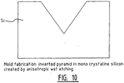
- Figure 10 Mold fabrication: inverted pyramid in mono crystalline silicon created by anisotropic wet etching.
- Figure 11 shows the conformal deposition of 3 layers: LPCVD. SiN, LPCVD Poly-Si, LPCVD SiN.
- Figure 12 shows the isotropic removal of the last deposited LPCVD SiN layer.
- Figure 13 shows the 1.23 times over-etching to remove the LPCVD SiN in the four oblique ribs of the inverted pyramid.
- Figure 14 shows the partly oxidation of the LPCVD poly-Si using the residual LPCVD SiN as inversion mask. (local oxidation of LPCVD poly-Si: LOCOS).
- Figure 15 shows the stripping of the residual LPCVD SiN.
- Figures 16 shows the wet etching of poly-Si using the LOCOS-oxide as mask material. Length A can be tuned by the etching time.
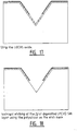
- Figure 17 shows the stripping of the LOCOS oxide.
- Figure 18 shows the isotropic etching of the first deposited LPCVD SiN layer using the polysilicon as the etch mask.
- Figure 19 shows the stripping of the poly-silicon layer.
- Figure 20 shows the conformal deposition of LPCVD poly Si (sacrificial layer).
- Figure 21 shows the conformal deposition of LPCVD SiN (capping layer of the fluid/gas channel).
- Figure 22 shows the sacrificial etching of the LPCVD poly-Si layer, leaving a channel for fluid/gas supply.
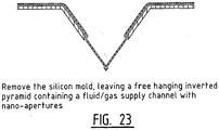
- Figure 23 shows the removal of the silicon mold, leaving a free hanging inverted pyramid containing a fluid/gas supply channel with nano-apertures.
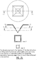
- Figure 24 is the top drawing represents the top view of the final structure: a SiN pyramid fountain pen with tunable nano-apertures.
- Cross section 1-1 represents figure 23 . Views 2) and 3) show different cross sections.
- the advantage of the fountain pen approach compared with NADIS is that a wider variety of inks can be used (also more volatile ones) and that eventually complex fluidic delivery systems can be made.
- some of the possible advantages of the fountain pen technology are: a larger amount of ink is available, the dependence of the writing process on relative humidity could be less, inks can be mixed at the tip, inks can possibly be changed during writing and electrochemical deposition of for example metals is possible.
- a cross-section of the prior art probe is shown in figure 25 below, together with a written line pattern of a self-assembled monolayer (ODT) on gold. As can be seen in fig. 25 , the written feature size is still in the order of 1 ⁇ m.
- the final aim in the scope of this proposal is a ten-fold reduction of the line width, so typically sub-100 nm resolution.
- the applicant has ongoing collaborations with the Biophysical Engineering Group of prof. Subramaniam and the Molecular Nanofabrication group of prof. Huskens (both at the university of Twente) on the application of the nanofountain pen, therefore knowledge of different inks and substrates to be tested is available to the project.
Landscapes
- Engineering & Computer Science (AREA)
- Chemical & Material Sciences (AREA)
- Manufacturing & Machinery (AREA)
- Radiology & Medical Imaging (AREA)
- Physics & Mathematics (AREA)
- Health & Medical Sciences (AREA)
- General Health & Medical Sciences (AREA)
- General Physics & Mathematics (AREA)
- Nuclear Medicine, Radiotherapy & Molecular Imaging (AREA)
- Analytical Chemistry (AREA)
- Microelectronics & Electronic Packaging (AREA)
- Nanotechnology (AREA)
- Crystallography & Structural Chemistry (AREA)
- Micromachines (AREA)
- Crystals, And After-Treatments Of Crystals (AREA)
- Semiconductor Memories (AREA)
- Cold Cathode And The Manufacture (AREA)
- Moulds For Moulding Plastics Or The Like (AREA)
- Mounting, Exchange, And Manufacturing Of Dies (AREA)
Description
- The present invention relates to a method for making a 3D nanostructure having a nanosubstructure, such as an insulating pyramid having a metallic tip.
- In nanotechnology the term "nano" means that the relevant dimension is less than 100nm. This implies that the 3D nanostructure and substructures may be typically a few microns large, but would be much smaller. In this application the term "nano" also encompasses structure with a relevant dimension up to 100 microns, preferably up to 50 microns or up to 10 microns. The lower limit is about 1nm, preferably about 5 or 10nm.
- Several fabrication strategies have been developed to define sub-micron features without the need for nano lithography. These include edge lithography to create 2D-confined nanochannels and nano-ridges (see N.R. Tas, J.W. Berenschot, P. Mela, H.V. Jansen, M. Elwenspoek, A. van den Berg, "2D-Confined Nanochannels Fabricated by Conventional Micromachining", Nano Lett., 2 (2002), pp. 1031-1032, and J. Haneveld, E. Berenschot, P. Maury, H. Jansen,"Nano-ridge fabrication by local oxidation of silicon edges with silicon nitride as a mask", J. Micromech. Microeng., 16 (2006), pp. S24-S28). Another fabrication strategy includes the use of stress induced retardation of oxide growth in corners to create nano-apertures (See A. Vollkopf, O. Rudow, M. Muller-Wiegand, G. Georgiev, E. Oesterschulze, "Influence of the oxidation temperature on the fabrication process of silicon dioxide aperture tips", Appl. Phys. A, 76 (2003), p. 923-926),and low temperature oxidation and selective etching (LOSE) to create an aperture at the apex of a pyramidal tip (see P.N. Minh, T. Ono, and M. Esashi, "Non-uniform silicon oxidation and application for the fabrication of aperture for near-field scanning optical microscopy", Appl. Phys. Lett., 75 (1999), pp. 4076-4078.
- Corner lithography was introduced and used to create a nano wire pyramid (see E. Sarajlic, E. Berenschot, G. Krijnen, M. Elwenspoek, "Fabrication of 3D Nanowire Frames by Conventional Micromachining Technology", Transducers '05 [Digest of techn. Papers 13th Int. Conf. on Solid-State Sensors, Actuators and Microsystems], pp. 27 - 29).
- Corner lithography is based on the material that is left in sharp concave corners after conformal deposition and isotropic etching. If t is the thickness of the deposited layer, α is the angle of the sharp concave corner, and R is the isotropic thinning distance, then the remaining material has a thickness w), given by:

- The present invention has for its object to provide a method for making 3D nanostructures having at least one nanosubstructure. The invention is based on the insight that by using corner lithography it is possible to create such nanosubstructures and nanowires without the need of nano lithography. To that extent structural material that remains after conformal deposition and subsequent isotropic thinning of a thin film in sharp concave corners is used as a mask. From the embodiment given it is clear that several steps are added, to create an inversion mask. As will be shown the method according to an example is a powerful technique for nano-patterning of pyramidal tips, as the ones used in scanning probe microscopy (SPM).
- Furthermore, pyramids provided with apertures can be used for liquid meniscus manipulation. The 3D oriented wires can be used for manipulating a liquid droplet. In addition, due to the 3D orientation these nanowires can be used for advanced measurements whereas effects typical for nanowires can now be determined in a 3D mode. By appropriate selection of material 3D fluidum (gas/liquid) channels can be made (see for 2D fluidum channels: N.R. Tas, J.W. Berenschot, P. Mela, H.V. Jansen, M. Elwenspoek, A..van den Berg, "2D-Confined Nanochannels Fabricated by Conventional Micromachining", Nano Lett., 2 (2002), pp. 1031-1032.
- Finally, provides a 3D coupling of nanowires (or nanochannels) a new combination of measured data in scanning probe microscopy.
- Accordingly, in view of the above objectives and desires the present invention provides a method for making a 3D nanostructure having a nanosubstructure according to
claim 1, comprising the steps of:
i) providing a mold comprising at least one sharp concave corner; ii) conformal depositing at least one structural material in at least the sharp concave corner; iii) isotropically removing structural material; iv) depositing at least one other structural material; v) removing earlier deposited structural material; vi) forming a nanosubstructure; and vii) removing the mold thereby providing the 3D nanostructure having the nanosubstructure. - A sharp concave corner has an angle which in principle is greater than 0° and less than 180°. More practically the angles lies between about 10° and about 170°. In practice for a silicon mold (made of silicon crystal) the crystal angles are at about 70°, 90° en 110°. Using other crystal structures for the mold will allow the use of different angles. In addition, an important (silicon) etching method for micromachining is the so called deep reactive ion etching (DRIE). DRIE etches substancially perpendicular to the (silicon) substrate. This implies that the angle will be in a range around 90°. Furhtermore, at angles close to 180° the differential overetching for selctively removing material will be more difficult. Thus, the angles could be within the range of 30° to 150°, such as 50° to 140°, or from 60° to 120°.
- According to a preferred embodiment the 3D nanostructure has a pyramidal form and the conformal deposition takes place in at least the pyramidal apex and/or rigdes. However, other 3D structures such as cones and pyramids with a triangular or multigonal base, are also possible.
- Different materials can be used as the structural material. Examples are polysilicon, silicon nitride and silicon oxide. Preferred are materials that can be conformally deposited using different methods and can be (isotropically) removed by different methods using conditions which are not negatively effecting the other applied materials. According to a preferred embodiment is in step iv) the other structural material deposited by local oxidation of the silicon mold and/or oxidation of a previously deposited structural material, such as poly silicon.
- According to a preferred embodiment is structural material directly or after isotropical (partial) removal used for defining a space for the nanostructure. To that extent the step vi) of forming the nanosubstructure may comprise a further material deposition, such as metal, plastic, porous material or mixtures thereof. More preferably the metal deposition results in the formation of an insulating pyramid having a metallic tip. Such metallic tip can be used as catalyst for e.g. carbon nanotube (- nanofiber) growth,as a local electrode for electrical or electrochemical measurement + stimulus, or for surface enhanced raman spectroscopy (SERS) measurements.
- In addition, the single hole at the apex can be used as a dopingmask. Mono crystalline silicon (or poly-Silicon) can be doped with boron. Accordingly, a boron doped p++ silicon nano-dot or line can be formed. Such structure conducts electricity well. Furthermore, this layer may be maintained when the mold is removed by etching. This results in the formation of a p++ nanodot or line. A metal contact can be provided to the top surface. When using this structure as a probe on a conductive surface it is possible to measure through the tip structure.
- Mentioned and other features of the method and 3D nanostructures according to the invention will be further illustrated by several examples which are given for information purposes only and are not intended to limit the invention to any extent. In relation to these embodiments reference will be made to the annexed figures of which:
-
Figure 1 shows a fabrication scheme for the silicon oxide pyramid containing a nanosubstructure in the form of a nanoscale metal tip; -
Figure 2 shows a silicon oxide pyramid containing a chromium tip as produced in example 1. -
Figure 3 is visualization of the fabrication scheme for the silicon nitride pyramid with nano-apertures. -
Figure 4 shows silicon nitride pyramid with apertures in all four side walls as produced in example 2. -
Figure 5 shows the mold fabrication for vertical nanowires. (a) silicon pillar formation and oxidation. (b) Cross section showing the corner sharpening. (c) anisotropic silicon oxide etching. (d) hollowing out of the mold structure. -
Figure 6 shows (Top:) a nanostructure containing vertical nanowires created through corner lithography. Note that wires have only been formed in the concave corners of the mold. (Bottom:) Close up of some of the vertical nanowires as produced in example 3. -
Figure 7 shows the mold fabrication for horizontal nanowires suspended by vertical nanowires. (a) Silicon etching. (b) under cutting the silicon nitride mask layer. (c) thinning down of the silicon nitride and subsequent LOCOS step. (d) isotropic etching of the silicon to form the hollow mold structure; -
Figure 8 silicon oxide mold, note the overhanging "roof"; and -
Figure 9 shows suspended silicon nitride nano wires created by corner lithography according to example 3. -
Figure 10 : Mold fabrication: inverted pyramid in mono crystalline silicon created by anisotropic wet etching; -
Figure 11 shows the conformal deposition of 3 layers: LPCVD SiN, LPCVD Poly-Si, LPCVD SiN; -
Figure 12 shows the isotropic removal of the last deposited LPCVD SiN layer; -
Figure 13 shows the 1.23 times over-etching to remove the LPCVD SiN in the four oblique ribs of the inverted pyramid; -
Figure 14 shows the partly oxidation of the LPCVD poly-Si using the residual LPCVD SiN as inversion mask. (local oxidation of LPCVD poly-Si: LOCOS); -
Figure 15 shows the stripping of the residual LPCVD SiN; -
Figures 16 shows the wet etching of poly-Si using the LOCOS-oxide as mask material. length A can be tuned by the etching time; -
Figure 17 shows the stripping of the LOCOS oxide; -
Figure 18 shows the isotropic etching of the first deposited LPCVD SiN layer using the polysilicon as the etch mask; -
Figure 19 shows the stripping of the poly-silicon layer; -
Figure 20 shows the conformal deposition of LPCVD poly Si (sacrificial layer); -
Figure 21 shows the conformal deposition of LPCVD SiN (capping layer of the fluid/gas channel); -
Figure 22 shows the sacrificial etching of the LPCVD poly-Si layer, leaving a channel for fluid/gas supply; -
Figure 23 shows the removal of the silicon mold, leaving a free hanging inverted pyramid containing a fluid/gas supply channel with nano-apertures; -
Figure 24 is the top drawing represents the top view of the final structure: a SiN pyramid fountain pen with tunable nano-apertures. Cross section 1-1 representsfigure 23 . Views 2) and 3) show different cross sections. -
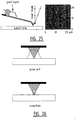
Figure 25 (Left) Cross section of a prior art nano fountain pen. The liquid (red) is transported from the reservoir to the pyramidal tip through the embedded nanochannel. (Right) Written line pattern of a self-assembled monolayer (ODT) on sputtered gold. The typical line width is 1 µm; and -
Figure 26 . (Left) In a locally "wet" environment a relative large meniscus (µm size) can be formed around the tip. (Right) It is expected that the apertures in the sides of the pyramid will help to confine the meniscus to the tip apex. - The materials mostly used in the examples as structural or masking material are polysilicon (Low Pressure Chemical Vapour Deposited, LPCVD), silicon oxide (thermal), and low stress (silicon rich) silicon nitride (LPCVD). Table 1 summarizes the etch rates of these materials in the etchants used in the examples. TMAH refers to a 5 wt% solution of tetramethyl ammonium hydroxide in water at 70 °C. 50% HF etching. is performed at room temperature, without stirring. H3PO4 refers to a 85 vol% solution at 180°C.
Table 1: Etch rates in nm/min Material Etchant Polysilicon Silicon nitride Silicon oxide TMAH 4-7e+02 * 1e-02 7e-02 HF 50% 4e-02 3.3e+00 2e+03 H3PO4 3e-01 4.3e+00 2.5e-01 *The lower value is for the lateral etch rate in confinement, specifically for the conditions presented below. The higher value is for the blank film. - The aim of this example is to create an insulating micro pyramid, with metallic tip. Ultimately this type of structure could find application in advanced SPM, for example for localized electrical or electrochemical measurements.
Fig. 1 shows the fabrication scheme for an oxide pyramid supporting a nanosubstruture metal tip. Fabrication started with the mold fabrication, in this case by KOH etching in a <100> silicon wafer to create the pyramidal hole bounded by the <111> planes. Next, silicon nitride (220 nm) was deposited by LPCVD (conformal deposition) and isotropically removed in 50% HF (84 min. at room temperature). This is a timed etch step which required a 1.23 times over-etching to remove the silicon nitride in the four oblique ribs of the pyramidal hole (α = 109.4°) and leaving only a small piece of silicon nitride at the tip. To calibrate the etching speed, a dummy wafer containing the same thickness of silicon nitride was etched in parallel. The silicon oxide structural material for the pyramid was formed by local oxidation of the silicon (LOCOS) (see J.A. Appels, E. Kooi, M.M. Paffen, J.J. H. Schatorje, W. Verkuylen, "Local oxidation of silicon and its applications in semiconductor-device technology", Philips Res. Rep., 25 (1970), pp. 118-132) using the residual silicon nitride as the inversion mask. The LOCOS step was a wet oxidation performed at 1000 °C for 35 min., resulting in a 270 nm layer. Next, the silicon nitride at the tip was removed in hot H3PO4 (30 min. at 180 °C) and 30 nm Chromium was deposited by sputtering to create the metal tip. Finally, the silicon mold was removed in TMAH. TMAH is a suitable etchant for this step as it has a high selectivity for silicon as compared to silicon oxide (table 1) [7].Fig. 2 shows the fabricated silicon oxide pyramid having a Chromium tip of less than 300 nm in size. - Dependent on the material of the pyramide wires, the pyramid may have particular uses. With wires made of piezoresistive material, such as p++ silicon nano-dot or line, the pyramide may be used for measuring (contact) forces. With wires made material having a temperature dependent electrical resistance, a pyramide may be used for local temperature measurement. Wire dissipating electrical power may be used for local heating.
- This example is not part of the invention.
- The aim of this example is to create a pyramid with tunable nanosubstructure apertures close to the tip. Fabrication started with KOH etching of the pyramidal mold in a <100> silicon wafer. Next, 500 nm LPCVD silicon nitride structural material was conformally deposited, followed by 330 nm LPCVD polysilicon. This layer acted as etching mask in later steps. A second layer of silicon nitride (120 nm) was deposited and isotropically etched in 50 %HF in order to remove all of the silicon nitride but a small remnant at the tip (
fig. 3a ). This remnant was used as an inversion mask in the LOCOS step (wet oxidation at 900°C for 10 min.) of the polysilicon (fig. 3b ). After removal of the silicon nitride remnant a timed etching of the polysilicon followed, which starts at the apex of the pyramid and moves up along its sides (fig. 3c ). The duration of this step determines the height of the nano apertures to be formed. Typically, a confined layer of 330 nm polysilicon etches laterally at a speed of 4.2·102 nm/min. in the 5 wt% TMAH solution supplied through a silicon oxide pinhole of sub 100 nm. Next the silicon oxide was removed and the first silicon nitride etched in 50% HF. This also is a timed etch step as it should leave the silicon nitride nano wires and the tip (fig. 3d ).Fig. 4 shows a typical fabrication result with apertures in the order of 1 µm in size. The size and the location of the apertures can be tuned by the thickness of in particular the silicon nitride layers and by the polysilicon etching time. - This example is not part of the invention.
- In this example vertical nanowires and suspended horizontal silicon nitride nanowires were created in the sharp concave corners of a silicon oxide mold. The suspended nanowires illustrate the ability to create relative long, slender and rather complex 3D-structures using corner lithography.
- To create vertical nanowires a silicon oxide mold was made containing the appropriate sharp concave corners. Illustrated is the process which was followed by a structure having four vertical wires created in the corners of a square mold. First a square silicon pillar is etched by deep reactive ion etching (DRIE) with photoresist as the mask material. Next, the resist is stripped and the wafer oxidized (wet oxidation at 950 °C) to form the silicon oxide mold (thickness of about 400 nm),
fig. 5a . Under these conditions convex corners in the silicon are sharpened as is illustrate by the cross section,fig. 5b (see R.B. Marcus, T.T. Sheng, "The oxidation of shaped silicon surfaces", J. Electrochem. Soc., 129 (1982), pp. 1278-1282). Finally, the silicon oxide is removed from the top by a maskless directional RIE step (fig. 5c ), and the mold is hollowed out by isotropic RIE in a SF6 plasma (fig. 5d ). This completes the mold fabrication. To create vertical wires a silicon nitride layer of 350 nm was deposited by LPCVD and etched back in hot H3PO4 for 83 min to leave the wires in the concave corners. Finally, the silicon oxide mould was removed in BHF and the vertical nanowires remained (fig. 6 ). Note that vertical nanowires are only formed in concave corners of the mold, therefore they are situated only at convex corners of the supporting structure after removal of the mold. - To add suspended horizontal nanowires an overhanging "roof" is added to the mold to create an horizontally oriented concave corner. The fabrication of the mold is illustrated in
fig. 7 . First a silicon pillar is etched by DRIE (Bosch process) using a silicon oxide and silicon nitride bi-layer as the mask. Next, the silicon oxide is etched in BHF, under-cutting the silicon nitride thin film. Then the silicon nitride is thinned down in hot H3PO4 until it is only left on top of the silicon oxide. Using the remaining mask material a LOCOS step is performed. After stripping of the silicon nitride and thinning down of the silicon oxide, the silicon is isotropically etched in a SF6 plasma through the window in the silicon oxide.Fig. 8 shows a SEM picture of a typical mold structure. The cross section next to it shows the location of the horizontal nanowires in the concave corners of the mold.Fig. 9 shows the resulting suspended nano wire structure formed after conformal deposition of silicon nitride (350 nm by LPCVD), subsequent isotropic thinning of this layer in hot H3PO4 for 83 min., and removal of the mold in BHF. - This example is not part of the invention.
- As in example 2 is first produced a SiN pyramid with tunable nano-apertures. Subsequently, by further two conformal depositions of structural materials and by sacrificial etching of the formerly deposited structural layer are formed channels for liquid or gas. Finally after removal of the the silicon mold, remains a free hanging inverted pyramid containing a fluid/gas supply channel with nano-apertures.
- With reference to the
figures 10-24 the method for making a silicon nitride pyramid fountain-pen is further described. -
Figure 10 : Mold fabrication: inverted pyramid in mono crystalline silicon created by anisotropic wet etching. -
Figure 11 shows the conformal deposition of 3 layers: LPCVD. SiN, LPCVD Poly-Si, LPCVD SiN. -
Figure 12 shows the isotropic removal of the last deposited LPCVD SiN layer. -
Figure 13 shows the 1.23 times over-etching to remove the LPCVD SiN in the four oblique ribs of the inverted pyramid. -
Figure 14 shows the partly oxidation of the LPCVD poly-Si using the residual LPCVD SiN as inversion mask. (local oxidation of LPCVD poly-Si: LOCOS). -
Figure 15 shows the stripping of the residual LPCVD SiN. -
Figures 16 shows the wet etching of poly-Si using the LOCOS-oxide as mask material. Length A can be tuned by the etching time. -
Figure 17 shows the stripping of the LOCOS oxide. -
Figure 18 shows the isotropic etching of the first deposited LPCVD SiN layer using the polysilicon as the etch mask. -
Figure 19 shows the stripping of the poly-silicon layer. -
Figure 20 shows the conformal deposition of LPCVD poly Si (sacrificial layer). -
Figure 21 shows the conformal deposition of LPCVD SiN (capping layer of the fluid/gas channel). -
Figure 22 shows the sacrificial etching of the LPCVD poly-Si layer, leaving a channel for fluid/gas supply. -
Figure 23 shows the removal of the silicon mold, leaving a free hanging inverted pyramid containing a fluid/gas supply channel with nano-apertures. -
Figure 24 is the top drawing represents the top view of the final structure: a SiN pyramid fountain pen with tunable nano-apertures. Cross section 1-1 representsfigure 23 . Views 2) and 3) show different cross sections. - The advantage of the fountain pen approach compared with NADIS (nanoscale dispensing system) is that a wider variety of inks can be used (also more volatile ones) and that eventually complex fluidic delivery systems can be made. Compared with the popular dip pen technology some of the possible advantages of the fountain pen technology are: a larger amount of ink is available, the dependence of the writing process on relative humidity could be less, inks can be mixed at the tip, inks can possibly be changed during writing and electrochemical deposition of for example metals is possible. A cross-section of the prior art probe is shown in
figure 25 below, together with a written line pattern of a self-assembled monolayer (ODT) on gold. As can be seen infig. 25 , the written feature size is still in the order of 1µm. The explanation for this is that most likely a local "wet" environment is created in the vicinity of the tip which, as described by the Kelvin equation, leads to a meniscus with a relative large radius of curvature. Depending on the contact angle of the ink to the substrate and the tip material, this can easily lead to a rather large spot on the substrate (fig. 26 (left) illustrates this). The strategy that we will follow to confine the meniscus is the use of the apertures on the four sides of the pyramid. It is expected that the meniscus is confined to the tip apex as illustrated infig. 26 (right). Liquid is supplied through the inside of the pyramid. A second approach is to guide the liquid in or along the wires of a wire pyramid structure. The final aim in the scope of this proposal is a ten-fold reduction of the line width, so typically sub-100 nm resolution. The applicant has ongoing collaborations with the Biophysical Engineering Group of prof. Subramaniam and the Molecular Nanofabrication group of prof. Huskens (both at the university of Twente) on the application of the nanofountain pen, therefore knowledge of different inks and substrates to be tested is available to the project. - In the above examples has been shown a fabrication process for 3D nanostructures comprising nanosubstructures without the need for nano lithography. As it is a batch-wise process which is relative cheap.
Claims (5)
- Method for making a 3D nanostructure having a nanosubstructure, comprising the steps of:i) providing a mold comprising at least one sharp concave corner;ii) conformal depositing at least one structural material in at least the sharp concave corner;iii) isotropically removing a first portion of said structural material, deposited in step ii), so that at least a second portion remains within the mold in the sharp concave corner;iv) depositing at least one other structural material in the mold, wherein said second portion is used as an inversion mask;v) removing the second portion of structural material, so that at least a third portion of the at least one other structural material remains within the mold;vi) thereafter forming a nanosubstructure by depositing a layer of structural material over the mold; andvii) removing the mold thereby providing the 3D nanostructure having the nanosubstructure.
- Method according to claim 1, wherein the mold is a pyramidal mold.
- Method according to claim 1 or 2, wherein in step iv) the other structural material is deposited by local oxidation of the silicon mold and/or oxidation of a previously deposited structural material, such as poly silicon.
- Method according to claim 1-3, wherein the step vi) of forming the nanosubstructure comprises deposition of a further material, such as a metal, plastic, porous material or mixtures thereof.
- Method according to claim 4, wherein the material deposition results in the formation of an insulating pyramid having a metallic tip.
Priority Applications (2)
| Application Number | Priority Date | Filing Date | Title |
|---|---|---|---|
| EP19171039.1A EP3549906A3 (en) | 2008-01-06 | 2008-12-22 | A method for making a 3d nanostructure having a nanosubstructure, such as an insulating pyramid having a metallic tip |
| EP08869344.5A EP2231507B1 (en) | 2008-01-06 | 2008-12-22 | A method for making a 3d nanostructure having a nanosubstructure, such as an insulating pyramid having a metallic tip |
Applications Claiming Priority (3)
| Application Number | Priority Date | Filing Date | Title |
|---|---|---|---|
| EP08000094A EP2077249A1 (en) | 2008-01-06 | 2008-01-06 | A method for making a 3D nanostructure having a nanosubstructure, and an insulating pyramid having a metallic tip, a pyramid having a nano-apertures and horizontal and/or vertical nanowires obtainable by this method |
| EP08869344.5A EP2231507B1 (en) | 2008-01-06 | 2008-12-22 | A method for making a 3d nanostructure having a nanosubstructure, such as an insulating pyramid having a metallic tip |
| PCT/EP2008/011107 WO2009086915A1 (en) | 2008-01-06 | 2008-12-22 | A method for making a 3d nanostructure having a nanosubstructure, and an insulating pyramid having a metallic tip, a pyramid having nano-apertures and horizontal and/or vertical nanowires obtainable by this method |
Related Child Applications (1)
| Application Number | Title | Priority Date | Filing Date |
|---|---|---|---|
| EP19171039.1A Division EP3549906A3 (en) | 2008-01-06 | 2008-12-22 | A method for making a 3d nanostructure having a nanosubstructure, such as an insulating pyramid having a metallic tip |
Publications (2)
| Publication Number | Publication Date |
|---|---|
| EP2231507A1 EP2231507A1 (en) | 2010-09-29 |
| EP2231507B1 true EP2231507B1 (en) | 2019-05-01 |
Family
ID=39408658
Family Applications (3)
| Application Number | Title | Priority Date | Filing Date |
|---|---|---|---|
| EP08000094A Withdrawn EP2077249A1 (en) | 2008-01-06 | 2008-01-06 | A method for making a 3D nanostructure having a nanosubstructure, and an insulating pyramid having a metallic tip, a pyramid having a nano-apertures and horizontal and/or vertical nanowires obtainable by this method |
| EP08869344.5A Active EP2231507B1 (en) | 2008-01-06 | 2008-12-22 | A method for making a 3d nanostructure having a nanosubstructure, such as an insulating pyramid having a metallic tip |
| EP19171039.1A Pending EP3549906A3 (en) | 2008-01-06 | 2008-12-22 | A method for making a 3d nanostructure having a nanosubstructure, such as an insulating pyramid having a metallic tip |
Family Applications Before (1)
| Application Number | Title | Priority Date | Filing Date |
|---|---|---|---|
| EP08000094A Withdrawn EP2077249A1 (en) | 2008-01-06 | 2008-01-06 | A method for making a 3D nanostructure having a nanosubstructure, and an insulating pyramid having a metallic tip, a pyramid having a nano-apertures and horizontal and/or vertical nanowires obtainable by this method |
Family Applications After (1)
| Application Number | Title | Priority Date | Filing Date |
|---|---|---|---|
| EP19171039.1A Pending EP3549906A3 (en) | 2008-01-06 | 2008-12-22 | A method for making a 3d nanostructure having a nanosubstructure, such as an insulating pyramid having a metallic tip |
Country Status (4)
| Country | Link |
|---|---|
| US (2) | US8932473B2 (en) |
| EP (3) | EP2077249A1 (en) |
| JP (1) | JP5501250B2 (en) |
| WO (1) | WO2009086915A1 (en) |
Families Citing this family (12)
| Publication number | Priority date | Publication date | Assignee | Title |
|---|---|---|---|---|
| EP2077249A1 (en) * | 2008-01-06 | 2009-07-08 | Universiteit Twente | A method for making a 3D nanostructure having a nanosubstructure, and an insulating pyramid having a metallic tip, a pyramid having a nano-apertures and horizontal and/or vertical nanowires obtainable by this method |
| FR2934709B1 (en) * | 2008-08-01 | 2010-09-10 | Commissariat Energie Atomique | THERMAL EXCHANGE STRUCTURE AND COOLING DEVICE HAVING SUCH A STRUCTURE. |
| EP2604175B1 (en) | 2011-12-13 | 2019-11-20 | EndoChoice Innovation Center Ltd. | Removable tip endoscope |
| US9334571B2 (en) | 2012-06-29 | 2016-05-10 | Regents Of The University Of Minnesota | Method of forming individual metallic microstructures |
| US10605827B2 (en) * | 2015-12-14 | 2020-03-31 | Universidade Federal De Menas Gerais-Ufmg | Metallic device for scanning probe microscopy and method for manufacturing same |
| US10689245B2 (en) | 2018-02-27 | 2020-06-23 | International Business Machines Corporation | Vertically stacked nanofluidic channel array |
| CN108673880A (en) * | 2018-06-13 | 2018-10-19 | 北京化工大学 | A kind of 3D printing interstitital texture and its processing technology with joinery and its construction |
| EP3552806A1 (en) | 2018-04-09 | 2019-10-16 | Nederlandse Organisatie voor toegepast- natuurwetenschappelijk onderzoek TNO | Method of apparatus for forming an object by means of additive manufacturing |
| NL2022939B1 (en) * | 2019-04-12 | 2020-10-20 | Smarttip Bv | A method of providing a MEMS device comprising a pyramidal protrusion, and a mold |
| CN112062084A (en) * | 2020-08-25 | 2020-12-11 | 华南理工大学 | A high-resolution silicon-based hollow cantilever probe and its preparation method |
| NL2026730B1 (en) * | 2020-10-22 | 2022-06-16 | Cytosurge Ag | A method of manufacturing a MEMS device |
| CN116715186B (en) * | 2023-03-03 | 2025-09-30 | 浙江大学 | Ciliary optical fluid sensor array and flow field testing method based on bionics |
Citations (1)
| Publication number | Priority date | Publication date | Assignee | Title |
|---|---|---|---|---|
| WO2004028952A2 (en) * | 2002-06-26 | 2004-04-08 | Cornell Research Foundation, Inc. | Small scale wires with microelectromechanical devices |
Family Cites Families (17)
| Publication number | Priority date | Publication date | Assignee | Title |
|---|---|---|---|---|
| JPH06117849A (en) * | 1992-10-07 | 1994-04-28 | Advantest Corp | Probe for spm and its manufacture |
| JP3226238B2 (en) * | 1993-03-15 | 2001-11-05 | 株式会社東芝 | Field emission cold cathode and method of manufacturing the same |
| US5584740A (en) * | 1993-03-31 | 1996-12-17 | The United States Of America As Represented By The Secretary Of The Navy | Thin-film edge field emitter device and method of manufacture therefor |
| KR100205051B1 (en) * | 1995-12-22 | 1999-06-15 | 정선종 | Method for manufacturing field emission display device |
| US5789272A (en) * | 1996-09-27 | 1998-08-04 | Industrial Technology Research Institute | Low voltage field emission device |
| JP3697034B2 (en) * | 1997-08-26 | 2005-09-21 | キヤノン株式会社 | Method of manufacturing protrusions having minute openings, and probes or multiprobes using them |
| JP2000123711A (en) * | 1998-10-12 | 2000-04-28 | Toshiba Corp | Field emission cold cathode and method of manufacturing the same |
| JP3884887B2 (en) * | 1999-08-27 | 2007-02-21 | 株式会社ルネサステクノロジ | Drawing probe and manufacturing method thereof |
| JP2001116678A (en) * | 1999-10-14 | 2001-04-27 | Canon Inc | Method for producing light irradiation or light detection probe, and light irradiation or light detection probe |
| GB2383187B (en) * | 2001-09-13 | 2005-06-22 | Microsaic Systems Ltd | Electrode structures |
| US6692145B2 (en) * | 2001-10-31 | 2004-02-17 | Wisconsin Alumni Research Foundation | Micromachined scanning thermal probe method and apparatus |
| AU2002348934A1 (en) * | 2002-01-15 | 2003-07-30 | International Business Machines Corporation | Microstructures |
| DE10236149A1 (en) * | 2002-08-05 | 2004-02-26 | Universität Kassel | Production of a structure having a sharp tip or cutting edge comprises providing a semiconductor substrate on a surface having a recess with a tip section, side walls and a layer, and deforming the substrate in the region of the recess |
| JP2004239704A (en) * | 2003-02-05 | 2004-08-26 | Renesas Technology Corp | Cantilever and its manufacturing method |
| GB0708695D0 (en) * | 2007-05-04 | 2007-06-13 | Univ Nottingham | Fabrication of nanoparticles |
| EP2077249A1 (en) * | 2008-01-06 | 2009-07-08 | Universiteit Twente | A method for making a 3D nanostructure having a nanosubstructure, and an insulating pyramid having a metallic tip, a pyramid having a nano-apertures and horizontal and/or vertical nanowires obtainable by this method |
| WO2010114887A1 (en) * | 2009-03-31 | 2010-10-07 | Georgia Tech Research Corporation | Metal-assisted chemical etching of substrates |
-
2008
- 2008-01-06 EP EP08000094A patent/EP2077249A1/en not_active Withdrawn
- 2008-12-22 JP JP2010541027A patent/JP5501250B2/en active Active
- 2008-12-22 US US12/811,674 patent/US8932473B2/en active Active
- 2008-12-22 EP EP08869344.5A patent/EP2231507B1/en active Active
- 2008-12-22 EP EP19171039.1A patent/EP3549906A3/en active Pending
- 2008-12-22 WO PCT/EP2008/011107 patent/WO2009086915A1/en not_active Ceased
-
2014
- 2014-12-15 US US14/570,652 patent/US9416001B2/en active Active
Patent Citations (1)
| Publication number | Priority date | Publication date | Assignee | Title |
|---|---|---|---|---|
| WO2004028952A2 (en) * | 2002-06-26 | 2004-04-08 | Cornell Research Foundation, Inc. | Small scale wires with microelectromechanical devices |
Also Published As
| Publication number | Publication date |
|---|---|
| JP5501250B2 (en) | 2014-05-21 |
| EP2077249A1 (en) | 2009-07-08 |
| US8932473B2 (en) | 2015-01-13 |
| WO2009086915A1 (en) | 2009-07-16 |
| US9416001B2 (en) | 2016-08-16 |
| EP3549906A2 (en) | 2019-10-09 |
| EP2231507A1 (en) | 2010-09-29 |
| JP2011511270A (en) | 2011-04-07 |
| US20150158724A1 (en) | 2015-06-11 |
| EP3549906A3 (en) | 2019-12-11 |
| US20110039100A1 (en) | 2011-02-17 |
Similar Documents
| Publication | Publication Date | Title |
|---|---|---|
| US8932473B2 (en) | Method for making a 3D nanostructure having a nanosubstructure, and an insulating pyramid having a metallic tip, a pyramid having nano-apertures and horizontal and/or vertical nanowires obtainable by this method | |
| Ziaie et al. | Introduction to micro-/nanofabrication | |
| US20160280537A1 (en) | Methods for fabricating high aspect ratio probes and deforming high aspect ratio nanopillars and micropillars | |
| US20100081278A1 (en) | Methods for Nanoscale Feature Imprint Molding | |
| US8828243B2 (en) | Scanning probe having integrated silicon tip with cantilever | |
| CN102205943A (en) | Preparation method of monocrystalline silicon nanostructure | |
| Zhao et al. | Sub-10 nm silicon ridge nanofabrication by advanced edge lithography for NIL applications | |
| Westerik et al. | Sidewall patterning—a new wafer-scale method for accurate patterning of vertical silicon structures | |
| US6887395B2 (en) | Method of forming sub-micron-size structures over a substrate | |
| Berenschot et al. | 3D-nanomachining using corner lithography | |
| Sarajlic et al. | Fabrication of 3D nanowire frames by conventional micromachining technology | |
| Mihalcea et al. | Reproducible large‐area microfabrication of sub‐100 nm apertures on hollow tips | |
| NL2026730B1 (en) | A method of manufacturing a MEMS device | |
| Boisen et al. | Indirect tip fabrication for scanning probe microscopy | |
| Berenschot et al. | A method for making a 3D nanostructure having a nanosubstructure, and an insulating pyramid having a metallic tip, a pyramid having nano-apertures and horizontal and/or vertical nanovires obtainable by this method | |
| Haneveld et al. | Nano-ridge fabrication by local oxidation of silicon edges with silicon nitride as a mask | |
| JP2005535137A (en) | Method for making at least one small opening in a layer on a substrate and component parts produced by such a method | |
| Golod et al. | Directional-rolling method for strained SiGe/Si films and its application to fabrication of hollow needles | |
| US11035880B2 (en) | Method for producing a probe suitable for scanning probe microscopy | |
| EP3953716B1 (en) | A method of providing a mems device comprising a pyramidal protrusion, and a mold | |
| Berenschot et al. | Wafer-scale nanostructure formation inside vertical nano-pores | |
| EP4228734B1 (en) | A method of manufacturing a micro-fluid probe | |
| Lin et al. | A liquid-based gravity-driven etching-stop technique and its application to wafer level cantilever thickness control of AFM probes | |
| Yifang et al. | Fabrication of nano-tips employing three different methods | |
| JPH1123590A (en) | Cantilever and manufacturing method thereof |
Legal Events
| Date | Code | Title | Description |
|---|---|---|---|
| PUAI | Public reference made under article 153(3) epc to a published international application that has entered the european phase |
Free format text: ORIGINAL CODE: 0009012 |
|
| 17P | Request for examination filed |
Effective date: 20100712 |
|
| AK | Designated contracting states |
Kind code of ref document: A1 Designated state(s): AT BE BG CH CY CZ DE DK EE ES FI FR GB GR HR HU IE IS IT LI LT LU LV MC MT NL NO PL PT RO SE SI SK TR |
|
| AX | Request for extension of the european patent |
Extension state: AL BA MK RS |
|
| STAA | Information on the status of an ep patent application or granted ep patent |
Free format text: STATUS: EXAMINATION IS IN PROGRESS |
|
| 17Q | First examination report despatched |
Effective date: 20161104 |
|
| GRAP | Despatch of communication of intention to grant a patent |
Free format text: ORIGINAL CODE: EPIDOSNIGR1 |
|
| STAA | Information on the status of an ep patent application or granted ep patent |
Free format text: STATUS: GRANT OF PATENT IS INTENDED |
|
| RIC1 | Information provided on ipc code assigned before grant |
Ipc: B81C 1/00 20060101AFI20181019BHEP Ipc: G01Q 70/16 20100101ALI20181019BHEP Ipc: G01Q 70/10 20100101ALI20181019BHEP |
|
| INTG | Intention to grant announced |
Effective date: 20181123 |
|
| RAP1 | Party data changed (applicant data changed or rights of an application transferred) |
Owner name: UNIVERSITEIT TWENTE |
|
| RIN1 | Information on inventor provided before grant (corrected) |
Inventor name: TAS, NIELS ROELOF Inventor name: BERENSCHOT, JOHAN WILLEM |
|
| GRAS | Grant fee paid |
Free format text: ORIGINAL CODE: EPIDOSNIGR3 |
|
| GRAA | (expected) grant |
Free format text: ORIGINAL CODE: 0009210 |
|
| STAA | Information on the status of an ep patent application or granted ep patent |
Free format text: STATUS: THE PATENT HAS BEEN GRANTED |
|
| AK | Designated contracting states |
Kind code of ref document: B1 Designated state(s): AT BE BG CH CY CZ DE DK EE ES FI FR GB GR HR HU IE IS IT LI LT LU LV MC MT NL NO PL PT RO SE SI SK TR |
|
| AX | Request for extension of the european patent |
Extension state: AL BA MK RS |
|
| REG | Reference to a national code |
Ref country code: GB Ref legal event code: FG4D |
|
| REG | Reference to a national code |
Ref country code: CH Ref legal event code: EP Ref country code: AT Ref legal event code: REF Ref document number: 1126675 Country of ref document: AT Kind code of ref document: T Effective date: 20190515 |
|
| REG | Reference to a national code |
Ref country code: DE Ref legal event code: R096 Ref document number: 602008059957 Country of ref document: DE |
|
| REG | Reference to a national code |
Ref country code: IE Ref legal event code: FG4D |
|
| REG | Reference to a national code |
Ref country code: CH Ref legal event code: NV Representative=s name: ARNOLD AND SIEDSMA AG, CH |
|
| REG | Reference to a national code |
Ref country code: NL Ref legal event code: FP |
|
| REG | Reference to a national code |
Ref country code: LT Ref legal event code: MG4D |
|
| PG25 | Lapsed in a contracting state [announced via postgrant information from national office to epo] |
Ref country code: LT Free format text: LAPSE BECAUSE OF FAILURE TO SUBMIT A TRANSLATION OF THE DESCRIPTION OR TO PAY THE FEE WITHIN THE PRESCRIBED TIME-LIMIT Effective date: 20190501 Ref country code: HR Free format text: LAPSE BECAUSE OF FAILURE TO SUBMIT A TRANSLATION OF THE DESCRIPTION OR TO PAY THE FEE WITHIN THE PRESCRIBED TIME-LIMIT Effective date: 20190501 Ref country code: NO Free format text: LAPSE BECAUSE OF FAILURE TO SUBMIT A TRANSLATION OF THE DESCRIPTION OR TO PAY THE FEE WITHIN THE PRESCRIBED TIME-LIMIT Effective date: 20190801 Ref country code: SE Free format text: LAPSE BECAUSE OF FAILURE TO SUBMIT A TRANSLATION OF THE DESCRIPTION OR TO PAY THE FEE WITHIN THE PRESCRIBED TIME-LIMIT Effective date: 20190501 Ref country code: FI Free format text: LAPSE BECAUSE OF FAILURE TO SUBMIT A TRANSLATION OF THE DESCRIPTION OR TO PAY THE FEE WITHIN THE PRESCRIBED TIME-LIMIT Effective date: 20190501 Ref country code: PT Free format text: LAPSE BECAUSE OF FAILURE TO SUBMIT A TRANSLATION OF THE DESCRIPTION OR TO PAY THE FEE WITHIN THE PRESCRIBED TIME-LIMIT Effective date: 20190901 Ref country code: ES Free format text: LAPSE BECAUSE OF FAILURE TO SUBMIT A TRANSLATION OF THE DESCRIPTION OR TO PAY THE FEE WITHIN THE PRESCRIBED TIME-LIMIT Effective date: 20190501 |
|
| PG25 | Lapsed in a contracting state [announced via postgrant information from national office to epo] |
Ref country code: BG Free format text: LAPSE BECAUSE OF FAILURE TO SUBMIT A TRANSLATION OF THE DESCRIPTION OR TO PAY THE FEE WITHIN THE PRESCRIBED TIME-LIMIT Effective date: 20190801 Ref country code: GR Free format text: LAPSE BECAUSE OF FAILURE TO SUBMIT A TRANSLATION OF THE DESCRIPTION OR TO PAY THE FEE WITHIN THE PRESCRIBED TIME-LIMIT Effective date: 20190802 Ref country code: LV Free format text: LAPSE BECAUSE OF FAILURE TO SUBMIT A TRANSLATION OF THE DESCRIPTION OR TO PAY THE FEE WITHIN THE PRESCRIBED TIME-LIMIT Effective date: 20190501 |
|
| REG | Reference to a national code |
Ref country code: AT Ref legal event code: MK05 Ref document number: 1126675 Country of ref document: AT Kind code of ref document: T Effective date: 20190501 |
|
| PG25 | Lapsed in a contracting state [announced via postgrant information from national office to epo] |
Ref country code: IS Free format text: LAPSE BECAUSE OF FAILURE TO SUBMIT A TRANSLATION OF THE DESCRIPTION OR TO PAY THE FEE WITHIN THE PRESCRIBED TIME-LIMIT Effective date: 20190901 |
|
| PG25 | Lapsed in a contracting state [announced via postgrant information from national office to epo] |
Ref country code: EE Free format text: LAPSE BECAUSE OF FAILURE TO SUBMIT A TRANSLATION OF THE DESCRIPTION OR TO PAY THE FEE WITHIN THE PRESCRIBED TIME-LIMIT Effective date: 20190501 Ref country code: DK Free format text: LAPSE BECAUSE OF FAILURE TO SUBMIT A TRANSLATION OF THE DESCRIPTION OR TO PAY THE FEE WITHIN THE PRESCRIBED TIME-LIMIT Effective date: 20190501 Ref country code: RO Free format text: LAPSE BECAUSE OF FAILURE TO SUBMIT A TRANSLATION OF THE DESCRIPTION OR TO PAY THE FEE WITHIN THE PRESCRIBED TIME-LIMIT Effective date: 20190501 Ref country code: AT Free format text: LAPSE BECAUSE OF FAILURE TO SUBMIT A TRANSLATION OF THE DESCRIPTION OR TO PAY THE FEE WITHIN THE PRESCRIBED TIME-LIMIT Effective date: 20190501 Ref country code: CZ Free format text: LAPSE BECAUSE OF FAILURE TO SUBMIT A TRANSLATION OF THE DESCRIPTION OR TO PAY THE FEE WITHIN THE PRESCRIBED TIME-LIMIT Effective date: 20190501 Ref country code: SK Free format text: LAPSE BECAUSE OF FAILURE TO SUBMIT A TRANSLATION OF THE DESCRIPTION OR TO PAY THE FEE WITHIN THE PRESCRIBED TIME-LIMIT Effective date: 20190501 |
|
| REG | Reference to a national code |
Ref country code: DE Ref legal event code: R097 Ref document number: 602008059957 Country of ref document: DE |
|
| PG25 | Lapsed in a contracting state [announced via postgrant information from national office to epo] |
Ref country code: IT Free format text: LAPSE BECAUSE OF FAILURE TO SUBMIT A TRANSLATION OF THE DESCRIPTION OR TO PAY THE FEE WITHIN THE PRESCRIBED TIME-LIMIT Effective date: 20190501 |
|
| PLBE | No opposition filed within time limit |
Free format text: ORIGINAL CODE: 0009261 |
|
| STAA | Information on the status of an ep patent application or granted ep patent |
Free format text: STATUS: NO OPPOSITION FILED WITHIN TIME LIMIT |
|
| PG25 | Lapsed in a contracting state [announced via postgrant information from national office to epo] |
Ref country code: TR Free format text: LAPSE BECAUSE OF FAILURE TO SUBMIT A TRANSLATION OF THE DESCRIPTION OR TO PAY THE FEE WITHIN THE PRESCRIBED TIME-LIMIT Effective date: 20190501 |
|
| 26N | No opposition filed |
Effective date: 20200204 |
|
| PG25 | Lapsed in a contracting state [announced via postgrant information from national office to epo] |
Ref country code: PL Free format text: LAPSE BECAUSE OF FAILURE TO SUBMIT A TRANSLATION OF THE DESCRIPTION OR TO PAY THE FEE WITHIN THE PRESCRIBED TIME-LIMIT Effective date: 20190501 |
|
| PG25 | Lapsed in a contracting state [announced via postgrant information from national office to epo] |
Ref country code: SI Free format text: LAPSE BECAUSE OF FAILURE TO SUBMIT A TRANSLATION OF THE DESCRIPTION OR TO PAY THE FEE WITHIN THE PRESCRIBED TIME-LIMIT Effective date: 20190501 |
|
| REG | Reference to a national code |
Ref country code: BE Ref legal event code: MM Effective date: 20191231 |
|
| PG25 | Lapsed in a contracting state [announced via postgrant information from national office to epo] |
Ref country code: MC Free format text: LAPSE BECAUSE OF FAILURE TO SUBMIT A TRANSLATION OF THE DESCRIPTION OR TO PAY THE FEE WITHIN THE PRESCRIBED TIME-LIMIT Effective date: 20190501 |
|
| PG25 | Lapsed in a contracting state [announced via postgrant information from national office to epo] |
Ref country code: LU Free format text: LAPSE BECAUSE OF NON-PAYMENT OF DUE FEES Effective date: 20191222 Ref country code: IE Free format text: LAPSE BECAUSE OF NON-PAYMENT OF DUE FEES Effective date: 20191222 |
|
| PG25 | Lapsed in a contracting state [announced via postgrant information from national office to epo] |
Ref country code: BE Free format text: LAPSE BECAUSE OF NON-PAYMENT OF DUE FEES Effective date: 20191231 |
|
| PG25 | Lapsed in a contracting state [announced via postgrant information from national office to epo] |
Ref country code: CY Free format text: LAPSE BECAUSE OF FAILURE TO SUBMIT A TRANSLATION OF THE DESCRIPTION OR TO PAY THE FEE WITHIN THE PRESCRIBED TIME-LIMIT Effective date: 20190501 |
|
| PG25 | Lapsed in a contracting state [announced via postgrant information from national office to epo] |
Ref country code: HU Free format text: LAPSE BECAUSE OF FAILURE TO SUBMIT A TRANSLATION OF THE DESCRIPTION OR TO PAY THE FEE WITHIN THE PRESCRIBED TIME-LIMIT; INVALID AB INITIO Effective date: 20081222 Ref country code: MT Free format text: LAPSE BECAUSE OF FAILURE TO SUBMIT A TRANSLATION OF THE DESCRIPTION OR TO PAY THE FEE WITHIN THE PRESCRIBED TIME-LIMIT Effective date: 20190501 |
|
| PGFP | Annual fee paid to national office [announced via postgrant information from national office to epo] |
Ref country code: NL Payment date: 20241230 Year of fee payment: 17 |
|
| PGFP | Annual fee paid to national office [announced via postgrant information from national office to epo] |
Ref country code: GB Payment date: 20241230 Year of fee payment: 17 |
|
| PGFP | Annual fee paid to national office [announced via postgrant information from national office to epo] |
Ref country code: FR Payment date: 20241230 Year of fee payment: 17 |
|
| PGFP | Annual fee paid to national office [announced via postgrant information from national office to epo] |
Ref country code: DE Payment date: 20241230 Year of fee payment: 17 |
|
| PGFP | Annual fee paid to national office [announced via postgrant information from national office to epo] |
Ref country code: CH Payment date: 20250108 Year of fee payment: 17 |