EP2230890A1 - Method for providing a conductive material structure on a carrier - Google Patents
Method for providing a conductive material structure on a carrier Download PDFInfo
- Publication number
- EP2230890A1 EP2230890A1 EP09155698A EP09155698A EP2230890A1 EP 2230890 A1 EP2230890 A1 EP 2230890A1 EP 09155698 A EP09155698 A EP 09155698A EP 09155698 A EP09155698 A EP 09155698A EP 2230890 A1 EP2230890 A1 EP 2230890A1
- Authority
- EP
- European Patent Office
- Prior art keywords
- carrier
- conductive material
- mask
- material structure
- previous
- Prior art date
- Legal status (The legal status is an assumption and is not a legal conclusion. Google has not performed a legal analysis and makes no representation as to the accuracy of the status listed.)
- Withdrawn
Links
- 239000004020 conductor Substances 0.000 title claims abstract description 65
- 238000000034 method Methods 0.000 title claims abstract description 41
- 239000000463 material Substances 0.000 claims abstract description 92
- 230000001678 irradiating effect Effects 0.000 claims abstract description 6
- 238000001465 metallisation Methods 0.000 claims abstract description 6
- 230000002708 enhancing effect Effects 0.000 claims description 22
- 230000007613 environmental effect Effects 0.000 claims description 12
- 229920000642 polymer Polymers 0.000 claims description 9
- 238000007639 printing Methods 0.000 claims description 9
- 238000007649 pad printing Methods 0.000 claims description 8
- 230000001413 cellular effect Effects 0.000 claims description 6
- 229910052751 metal Inorganic materials 0.000 claims description 6
- 239000002184 metal Substances 0.000 claims description 6
- 239000003153 chemical reaction reagent Substances 0.000 claims description 5
- 238000004891 communication Methods 0.000 claims description 5
- 239000000835 fiber Substances 0.000 claims description 4
- 238000007747 plating Methods 0.000 claims description 4
- 230000005855 radiation Effects 0.000 claims description 3
- 238000001035 drying Methods 0.000 claims description 2
- 239000010410 layer Substances 0.000 description 12
- PXHVJJICTQNCMI-UHFFFAOYSA-N Nickel Chemical compound [Ni] PXHVJJICTQNCMI-UHFFFAOYSA-N 0.000 description 10
- 230000003213 activating effect Effects 0.000 description 8
- 229920003023 plastic Polymers 0.000 description 7
- 230000001681 protective effect Effects 0.000 description 7
- 239000000969 carrier Substances 0.000 description 6
- 238000000465 moulding Methods 0.000 description 6
- 239000000758 substrate Substances 0.000 description 6
- 230000008901 benefit Effects 0.000 description 5
- PCHJSUWPFVWCPO-UHFFFAOYSA-N gold Chemical compound [Au] PCHJSUWPFVWCPO-UHFFFAOYSA-N 0.000 description 5
- 229910052737 gold Inorganic materials 0.000 description 5
- 239000010931 gold Substances 0.000 description 5
- 229910052759 nickel Inorganic materials 0.000 description 5
- 239000011241 protective layer Substances 0.000 description 5
- XLYOFNOQVPJJNP-UHFFFAOYSA-N water Substances O XLYOFNOQVPJJNP-UHFFFAOYSA-N 0.000 description 5
- KDLHZDBZIXYQEI-UHFFFAOYSA-N Palladium Chemical compound [Pd] KDLHZDBZIXYQEI-UHFFFAOYSA-N 0.000 description 4
- 238000013461 design Methods 0.000 description 4
- 238000007650 screen-printing Methods 0.000 description 4
- PEZNEXFPRSOYPL-UHFFFAOYSA-N (bis(trifluoroacetoxy)iodo)benzene Chemical compound FC(F)(F)C(=O)OI(OC(=O)C(F)(F)F)C1=CC=CC=C1 PEZNEXFPRSOYPL-UHFFFAOYSA-N 0.000 description 3
- BQCADISMDOOEFD-UHFFFAOYSA-N Silver Chemical compound [Ag] BQCADISMDOOEFD-UHFFFAOYSA-N 0.000 description 3
- 229910052709 silver Inorganic materials 0.000 description 3
- 239000004332 silver Substances 0.000 description 3
- RYGMFSIKBFXOCR-UHFFFAOYSA-N Copper Chemical compound [Cu] RYGMFSIKBFXOCR-UHFFFAOYSA-N 0.000 description 2
- 239000004372 Polyvinyl alcohol Substances 0.000 description 2
- XUIMIQQOPSSXEZ-UHFFFAOYSA-N Silicon Chemical compound [Si] XUIMIQQOPSSXEZ-UHFFFAOYSA-N 0.000 description 2
- 230000004913 activation Effects 0.000 description 2
- 230000008859 change Effects 0.000 description 2
- 238000007796 conventional method Methods 0.000 description 2
- 229910052802 copper Inorganic materials 0.000 description 2
- 239000010949 copper Substances 0.000 description 2
- 238000005260 corrosion Methods 0.000 description 2
- 230000007797 corrosion Effects 0.000 description 2
- 230000001419 dependent effect Effects 0.000 description 2
- 238000007598 dipping method Methods 0.000 description 2
- 238000007772 electroless plating Methods 0.000 description 2
- 238000009713 electroplating Methods 0.000 description 2
- 239000000383 hazardous chemical Substances 0.000 description 2
- 229910001385 heavy metal Inorganic materials 0.000 description 2
- 238000007641 inkjet printing Methods 0.000 description 2
- 239000007788 liquid Substances 0.000 description 2
- 230000000873 masking effect Effects 0.000 description 2
- 229910052763 palladium Inorganic materials 0.000 description 2
- 229920002451 polyvinyl alcohol Polymers 0.000 description 2
- 229940068984 polyvinyl alcohol Drugs 0.000 description 2
- 235000019422 polyvinyl alcohol Nutrition 0.000 description 2
- 229910052710 silicon Inorganic materials 0.000 description 2
- 239000010703 silicon Substances 0.000 description 2
- 238000012360 testing method Methods 0.000 description 2
- 239000004923 Acrylic lacquer Substances 0.000 description 1
- ATJFFYVFTNAWJD-UHFFFAOYSA-N Tin Chemical compound [Sn] ATJFFYVFTNAWJD-UHFFFAOYSA-N 0.000 description 1
- 239000004904 UV filter Substances 0.000 description 1
- 238000013459 approach Methods 0.000 description 1
- 239000007795 chemical reaction product Substances 0.000 description 1
- 239000003638 chemical reducing agent Substances 0.000 description 1
- 238000005229 chemical vapour deposition Methods 0.000 description 1
- 150000004696 coordination complex Chemical class 0.000 description 1
- 230000000694 effects Effects 0.000 description 1
- 239000012777 electrically insulating material Substances 0.000 description 1
- 238000004519 manufacturing process Methods 0.000 description 1
- 239000007769 metal material Substances 0.000 description 1
- 150000002739 metals Chemical class 0.000 description 1
- 239000002245 particle Substances 0.000 description 1
- 229920000728 polyester Polymers 0.000 description 1
- 238000006722 reduction reaction Methods 0.000 description 1
- 230000000717 retained effect Effects 0.000 description 1
- 239000000523 sample Substances 0.000 description 1
- 238000005507 spraying Methods 0.000 description 1
- 238000004544 sputter deposition Methods 0.000 description 1
- 239000000126 substance Substances 0.000 description 1
- 229910052718 tin Inorganic materials 0.000 description 1
- 239000011135 tin Substances 0.000 description 1
- 239000002699 waste material Substances 0.000 description 1
Images



Classifications
-
- H—ELECTRICITY
- H05—ELECTRIC TECHNIQUES NOT OTHERWISE PROVIDED FOR
- H05K—PRINTED CIRCUITS; CASINGS OR CONSTRUCTIONAL DETAILS OF ELECTRIC APPARATUS; MANUFACTURE OF ASSEMBLAGES OF ELECTRICAL COMPONENTS
- H05K3/00—Apparatus or processes for manufacturing printed circuits
- H05K3/10—Apparatus or processes for manufacturing printed circuits in which conductive material is applied to the insulating support in such a manner as to form the desired conductive pattern
- H05K3/18—Apparatus or processes for manufacturing printed circuits in which conductive material is applied to the insulating support in such a manner as to form the desired conductive pattern using precipitation techniques to apply the conductive material
- H05K3/181—Apparatus or processes for manufacturing printed circuits in which conductive material is applied to the insulating support in such a manner as to form the desired conductive pattern using precipitation techniques to apply the conductive material by electroless plating
- H05K3/182—Apparatus or processes for manufacturing printed circuits in which conductive material is applied to the insulating support in such a manner as to form the desired conductive pattern using precipitation techniques to apply the conductive material by electroless plating characterised by the patterning method
- H05K3/185—Apparatus or processes for manufacturing printed circuits in which conductive material is applied to the insulating support in such a manner as to form the desired conductive pattern using precipitation techniques to apply the conductive material by electroless plating characterised by the patterning method by making a catalytic pattern by photo-imaging
-
- H—ELECTRICITY
- H05—ELECTRIC TECHNIQUES NOT OTHERWISE PROVIDED FOR
- H05K—PRINTED CIRCUITS; CASINGS OR CONSTRUCTIONAL DETAILS OF ELECTRIC APPARATUS; MANUFACTURE OF ASSEMBLAGES OF ELECTRICAL COMPONENTS
- H05K1/00—Printed circuits
- H05K1/02—Details
- H05K1/0213—Electrical arrangements not otherwise provided for
- H05K1/0237—High frequency adaptations
-
- H—ELECTRICITY
- H05—ELECTRIC TECHNIQUES NOT OTHERWISE PROVIDED FOR
- H05K—PRINTED CIRCUITS; CASINGS OR CONSTRUCTIONAL DETAILS OF ELECTRIC APPARATUS; MANUFACTURE OF ASSEMBLAGES OF ELECTRICAL COMPONENTS
- H05K2203/00—Indexing scheme relating to apparatus or processes for manufacturing printed circuits covered by H05K3/00
- H05K2203/05—Patterning and lithography; Masks; Details of resist
- H05K2203/0548—Masks
- H05K2203/0551—Exposure mask directly printed on the PCB
Definitions
- the present invention relates to the provision of a conductive material structure on a carrier, such as a structure defining conductors and/or radiators.
- Electrically conductive structures are known to be provided on carriers such as circuit boards. However, there is also a need for providing such structures on flex films, chassis, covers, casings or middle decks of a piece of electronic equipment, like a cellular phone. In some cases the structure is to function as a radiator or antenna. When it is provided as such it is important that the structure is well defined or otherwise the radiation properties may be worse than expected.
- LDS Laser Direct Structuring
- moulding is performed using two polymers in two moulding tools, where one polymer can be metallised and the other cannot.
- Such tools are expensive and it is therefore undesirable to change the structure too often.
- a carrier produced this way is furthermore thick, which is disadvantageous if it is to be used in a small portable electronic communications device, such as a cellular phone, where size restrictions are often severe.
- An object of the present invention is therefore to provide a method for providing a conductive material structure on a carrier using photo sensitive material, which method can achieve a well-defined conductive material structure regardless of the preciseness of light sources used.
- the invention is based on the realization that a mask that defines a conductive material structure can be applied on a photo sensitive material provided on the carrier. In this way it is possible to use less precise, and hence more economical, light sources for activating the photo sensitive material in order to metallise the defined structure.
- the invention presents a method for providing a conductive material structure on a carrier where the problem of achieving a well-defined conductive material structure regardless of the preciseness of the light sources used is solved through applying a photo sensitive material on the carrier, applying a mask on this photo sensitive material, where the mask defines a conductive material structure to be formed on the carrier, irradiating the defined structure on the carrier in order to prepare for metallisation and metalizing the defined structure for forming the conductive material structure.
- the present invention is generally directed towards the provision of conductive material structures on carriers, i.e. of material structures that are able to conduct electrical currents.
- Such structures can be conductors or antenna radiator traces provided on circuit boards, flex films, chassis, covers, casings or middle decks of a piece of electronic equipment.
- a piece of electronic equipment where such a carrier having a conductive material structure may be provided can be such a thing as a portable electronic device, like a gaming machine or an electronic organizer.
- a portable electronic device may also be a portable communication device such as a cellular phone, a lap top or a desk top computer.
- such a carrier with conductive material structure is provided as a mounting entity, which is to be mounted as one piece in such a piece of electronic equipment.
- the conductive material structure of the present invention may then be provided on the exterior of this entity, like on the surface of it. This means that the carrier in this case will become an outer surface of such a mounting entity.
- the present invention is therefore directed towards an alternative method for providing a conductive material structure on a carrier, which method achieves a well-defined conductive material structure regardless of the preciseness of the light sources used.
- the material structure that is to be provided on the carrier will in the following be exemplified through a radiator structure, i.e. the structure and shape of an antenna element.
- the exemplifying radiator structure shown is furthermore in the form of a Planar Inverted-F multiband antenna (multiband PIFA). It has to be emphasized that the shown radiator structure is only exemplifying and the present invention can be used on any radiator structure.
- a conductive material structure may also include more than one antenna.
- the conductive material structure is actually not limited to antennas at all but may be any conductive material structure provided on a carrier. It may for instance be the conductors and component contact points provided on a printed circuit board (PCB), i.e. the layout of a PCB.
- PCB printed circuit board
- Such a structure may be a conductive structure provided on carrier in the form of a printed circuit board (PCB) or a flex film. In these cases the structure is normally a two-dimensional structure provided on a planar surface of carrier
- the carrier may have a three-dimensional extension, i.e. it may extend in three dimensions.
- a three-dimensional conductive material structure may be provided on a curved surface of a carrier or on two planar surfaces of a carrier that are provided at an angle to each other, like an exemplifying angle of ninety degrees.
- Such a surface or surfaces may be the exterior or a part of the exterior of a mounting entity, like for instance a chassis.
- fig. 1 - 16 show the carrier during various process steps in the method
- fig. 17 shows a flow chart outlining a number of method steps being taken in one embodiment of the present invention, when producing a conductive material structure on a carrier.
- a carrier 10 which is shown in a top view in fig. 1 and in a side view in fig. 9 .
- the carrier 10 may be provided in the form of a dielectric substrate 10 that may be silicon based or made of a plastic material.
- the method starts through applying a photo sensitive material 12 on the carrier 10, step 24.
- This photo sensitive material 12 may cover the whole or only a part of the carrier 10. It is important that it covers an area on the carrier 10 where a radiator structure is to be provided.
- the photo sensitive material layer 11 is in this embodiment water soluble and is applied through printing it on the carrier 10. It should be realized that it is not limited to being soluble in water, but it may also be soluble in other liquids. It may in fact not be soluble at all.
- non-activated photo sensitive material can be removed irrespective of the properties allowing such removal.
- the photo sensitive material may here be advantageous with screen printing or pad printing.
- the photo sensitive material here typically includes a polymer and possibly also a reagent.
- the carrier with applied photo sensitive material 11 is schematically shown in fig. 2 and 10 . After the photo sensitive material has been applied, it is thereafter dried, step 26. This drying step is optional depending on if later steps can be performed using moist photo sensitive material or not.
- a mask 12 is applied on the photo sensitive material.
- the mask is a chemical mask, for instance being sprayed over the photo sensitive material.
- various types of printing for instance ink-jet printing, screen printing or pad printing. The printing is here with advantage pad printing. Alternatively a mechanical mask may also be used.
- pad printing is of special interest in case the structure is to be provided on a curved carrier surface, since pad printing uses a pad that receives material according to a desired structure on a pad, which is then pressed onto a surface that can have any shape.
- the pad here adapts its shape to the shape of carrier, which means that a conductive material structure may be provided on a curved carrier surface.
- Such a position may be of advantage in many portable electronic devices that need to be kept small. This therefore means that the volume in the interior of such a device, like a cellular phone, is used more efficiently.
- screen printing can work, where the carrier may be turned for printing on different sides of the carrier.
- a mask 12 is furthermore applied through selectively printing it on the photo sensitive material 11, step 28, in order to define the desired radiator structure.
- the mask 12 may here be water soluble in order to simplify application and later removal. It should be realized that it is not limited to being soluble in water, but it may also be soluble in other liquids. It may in fact not be soluble at all. What is important though is that the mask can be removed irrespective of the properties allowing such removal.
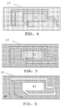
- the carrier 10 with photo sensitive material 11 and mask 12 is schematically shown in fig. 4 and 11 . In the present embodiment the mask 12 is applied so that the area where the radiator structure is to be provided is exposed. There is in this embodiment no mask 12 placed on the part of the carrier 10 where the actual radiator structure is to appear.
- the mask 12 thus has a pattern that overlaps the photo sensitive material and this pattern defines openings in the mask material, which openings in turn define the radiator structure.
- the mask 12 can also be seen as defining where the edges of the conductive material structure are to be provided. In this way the mask 12 thus defines the conductive material structure that is to be formed on the carrier 10.
- the mask here has activating wavelength filter properties, i.e. it filters away light at an activating wavelength of the photo sensitive material and may be made of a PVA (Poly Vinyl Alcohol) or similar material. In this embodiment, the activating wavelength lies in the UV (Ultra Violet) range and therefore the mask has UV filter properties.
- the mask is dried, step 30. Also this step is optional depending on if later steps can be provided on moist or dry mask material.
- this material is irradiated with light including the activating wavelength for being activated, step 32, which may be done using a UV lamp, a UV laser or other suitable UV source with a suitable wavelength.
- the wavelength may for instance be in the range of 200 - 1000 nm, 500 - 1000 nm or even round 266 or 355 nm.
- the irradiation causes a reagent to bind the polymer of the photo sensitive material to the carrier. Such a reagent may already be a part of the photo sensitive material.
- the polymer does furthermore have fibre strands on which the conductive material that is to form the structure is to attach.
- Activation may also need the use of an activating metal material, which may be provided in a solution, like a solution of Palladium that may be added through dipping the carrier in the solution.
- the activating material here assists in the attachment of the conductive material to the fibre strands.
- the activated state of the photo sensitive material 11 is indicated in fig. 4 and 12 .
- the irradiation is optionally followed by removal of residues or residual material, step 34, i.e. removal of the mask and non-activated photo sensitive material. This may be done by rinse, mechanical brush wash or other suitable wash technique.
- the carrier after such removal is shown in fig. 5 and 13 .
- the radiator structure is formed through metallization of the irradiated and activated area, step 36.
- the structure is thus metalized for forming the conductive material structure.
- Metallization may be performed through plating of a metal like copper. Other possible materials are Nickel, Silver or Palladium. It should be realized that this plating may be electroless plating or electroplating.
- Fig. 6 and 14 show the thus formed radiator structure 13 on the carrier 10. In any event, since the polymer is bound to the carrier, conductive material being applied to the fibre strands will be retained on the carrier.
- the structure 13 includes at least one contact area, i.e. an area where the structure is to be connected to another entity, such as for instance to a conductor, to a circuit, to a circuit board, to a component etc. Since the structure according to the present example is a PIFA, two such areas 14 and 16 are provided on this structure 13. Naturally there may be more or fewer such areas for other types of conductive material structures. In the case of PIFA one such area 14 is a signal connection area for connection to a radio circuit and the other 16 is a ground connection area for connection to a ground potential. The connection to the radio circuit and to the ground potential may both be provided via a circuit board provided separately from the carrier 10.
- the thus formed structure may be the final structure. However, in this case it is the subject of environmental hazards such as corrosion and moisture.
- the conductive material structure may therefore need an environmental protection layer or an environmental protection cover that protects it from this environment, such as protecting it from air, dirt and/or water. It may also need contact enhancing material in the above-mentioned contact areas, where such contact enhancing material may act to lower the contact resistance in connections to other entities such as components and circuits in the electronic device.
- the environmental protection layer and contact enhancing material may be provided using conventional techniques and methods. The traditional way that such a protection layer and contact enhancing material are provided is through providing the whole conductive material structure with contact enhancing material and thereafter the conductive material structure is covered with a protection layer. This has the disadvantage in that an excessive amount of contact enhancing material is used. This may be very expensive, especially if the contact enhancing material used is gold.
- the radiator structure may according to the present invention be covered with an environmental protection layer or protective cover 18 except for in a set of areas including at least one contact area and here the two contact areas 14 and 16, step 38.
- the radiator structure with protective cover is shown in fig. 7 and 15 .
- This protective cover 18 is here furthermore provided onto a side of this conductive material structure 13 that faces away from the carrier 10.
- a protective layer is provided over the parts of the structure that are to be insulated and not areas to be used for contacting other devices or for performing other activities, such as probe areas for testing.
- a mask of protective material may be sprayed or printed, for instance using ink-jet printing, screen printing or pad printing.
- the protection layer 18 is printed over the radiator structure 13 except for in the contact areas.
- the printing is here furthermore with advantage pad printing.
- the material may here be a plastic material. It may also in some cases be a metal such as gold, silver or nickel that does not corrode easily. It may also be a combination of gold and nickel.
- An electrically insulating material, like a plastic material may be advantageous for cost reasons. This material may be an acrylic lacquer or polyester.
- the mask is here selected so that it protects the underlying structure from environmental hazards such as corrosion and/or moisture.
- the use of plastic has another advantage. It will provide electrostatic discharge (ESD) protection from other components in the device. If the structure is an antenna the influence on the antenna efficiency and the radio frequency (RF) properties will then be limited.
- ESD electrostatic discharge
- a masking technique such as for instance to deposit the protective material over all the structure, provide a mask over the parts that are to retain the protective material, remove the protective material from the non-masked areas and then remove the mask material.
- electrical contact enhancing material 20, 22 is placed in the uncovered contact areas 14 and 16 of the structure 13, step 28.
- the placing of electrical contact enhancing material is thus performed after the conductive material structure 13 has been covered with the environmental protection layer 18.
- the structure 13 covered by a protective layer 18 with electrical contact enhancing material 20 and 22 over contact areas 14 and 16 is schematically shown in fig. 8 and 16 .
- the material may be placed in these contact areas through plating, like electroless plating or electroplating, sputtering or chemical vapour deposition.
- the protective layer 18 acts as a mask that stops the other parts of the structure from receiving contact enhancing material.
- the contact enhancing material may here be a metal such as gold, silver, nickel or tin or a combination of such metals such as a combination of gold and nickel.
- the method of providing a conductive material structure of the present invention allows flexibility in the design of the structure combined with simple tools for defining the radiator structure. It is for instance possible to only use a simple two-dimensional cliché for providing a mask that defines the radiator structure. Even though such a cliché is used for providing a mask a well defined radiator structure is obtained.
- the light sources used for irradiating the photo sensitive material need therefore not be well focused to the area covered for obtaining a well-defined radiator structure. Neither do the light sources have to be precise regarding wavelength as long as the activating wavelength is included.
- the invention can therefore also be implemented using inexpensive light sources for irradiating the photo sensitive material. This is furthermore combined with enabling a provision of thin carriers and without having to compromise the exactness of the conductive material structure. Since the tools for providing a mask can be simple and inexpensive, it is easy to change design through merely exchanging one cliché for another. The present invention therefore also allows the provision of more flexible production.
- the cover that is used for protecting the structure in the end product that is to be mounted in an electronic device acts as a mask when providing contact enhancing material. This means that the amount of contact enhancing material used is reduced. This also means that contact enhancing material is limited to what is necessary for ensuring contact at areas of the structure where contact is desired. This is also done without using additional process steps.
- the printed environmental protection layer has a further advantage. It can be used for providing an aesthetically interesting surface on the carrier.
- the surface may through this printing be provided with a graphical design, such as a company logotype, a figure or some other type of design. It can also be used for providing characters such as text and numbers and can therefore provide written and/or graphical messages.
- the set of areas that are to be excluded from being covered by the protective layer includes electrical contact areas for connection to other entities in the electronic equipment.
- this set may include also other areas such as probing areas that are to be used for testing the contact material structure. Such probing areas may or may not receive contact enhancing material.
Landscapes
- Engineering & Computer Science (AREA)
- Chemical & Material Sciences (AREA)
- Chemical Kinetics & Catalysis (AREA)
- Manufacturing & Machinery (AREA)
- Microelectronics & Electronic Packaging (AREA)
- Manufacturing Of Printed Wiring (AREA)
- Printing Plates And Materials Therefor (AREA)
Abstract
Description
- The present invention relates to the provision of a conductive material structure on a carrier, such as a structure defining conductors and/or radiators.
- Electrically conductive structures are known to be provided on carriers such as circuit boards. However, there is also a need for providing such structures on flex films, chassis, covers, casings or middle decks of a piece of electronic equipment, like a cellular phone. In some cases the structure is to function as a radiator or antenna. When it is provided as such it is important that the structure is well defined or otherwise the radiation properties may be worse than expected.
- There are some ways in which electrically conductive structures are provided on carriers, like carriers made from silicon or plastic substrates.
- One way in which they may be applied is through the use of Laser Direct Structuring (LDS), where a plastic material that is doped with particles of electrically conductive material, like copper, is irradiated with laser light. This laser light then causes the metal to appear on the surface of the plastic material. This allows the provision of a well defined structure. However, lasers are fairly expensive equipment.
- One example of using LDS is described in
WO 0035259 - Another example is through Two Shot Moulding. In this method moulding is performed using two polymers in two moulding tools, where one polymer can be metallised and the other cannot. Such tools are expensive and it is therefore undesirable to change the structure too often. A carrier produced this way is furthermore thick, which is disadvantageous if it is to be used in a small portable electronic communications device, such as a cellular phone, where size restrictions are often severe.
- There is therefore a need for an alternative way to provide a well defined conductive material structure on a carrier using photo sensitive material.
- An object of the present invention is therefore to provide a method for providing a conductive material structure on a carrier using photo sensitive material, which method can achieve a well-defined conductive material structure regardless of the preciseness of light sources used.
- The invention is based on the realization that a mask that defines a conductive material structure can be applied on a photo sensitive material provided on the carrier. In this way it is possible to use less precise, and hence more economical, light sources for activating the photo sensitive material in order to metallise the defined structure.
- According to a first aspect of the present invention there is provided a method as defined in claim 1.
- Further preferred embodiments are defined in the dependent claims.
- The invention presents a method for providing a conductive material structure on a carrier where the problem of achieving a well-defined conductive material structure regardless of the preciseness of the light sources used is solved through applying a photo sensitive material on the carrier, applying a mask on this photo sensitive material, where the mask defines a conductive material structure to be formed on the carrier, irradiating the defined structure on the carrier in order to prepare for metallisation and metalizing the defined structure for forming the conductive material structure.
- The invention is now described, by way of example, with reference to the accompanying drawings, in which:
-
fig. 1 shows a top view of a carrier acting as a substrate for a conductive material structure to be formed; -
fig. 2 shows a top view of a carrier on which a photo sensitive material layer has been printed; -
fig. 3 shows a top view of the carrier where a mask has been printed on top of the photo sensitive material layer; -
fig. 4 shows a top view of the carrier with mask after irradiation with UV light on exposed photo sensitive material; -
fig. 5 shows a top view of the carrier with remaining photo sensitive material after removal of residues; -
fig. 6 shows a top view of the carrier after metallization of the remaining photo sensitive material for forming the conductive material structure; -
fig. 7 shows a top view of the carrier, where the conductive material structure has been covered by a an environmental protection layer; -
fig. 8 shows a top view of the covered material structure, where contact areas of it have received electrical contact enhancing material; -
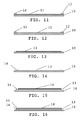
fig. 9 shows a side view of the carrier infig. 1 ; -
fig. 10 shows a side view of the carrier infig. 2 ; -
fig. 11 shows a side view of the carrier infig. 3 ; -
fig. 12 shows a side view of the carrier infig. 4 ; -
fig. 13 shows a side view of the carrier infig. 5 ; -
fig. 14 shows a side view of the carrier infig. 6 ; -
fig. 15 shows a side view of the carrier infig. 7 ; -
fig. 16 shows a side view of the carrier infig. 8 ; and -
fig. 17 shows a flow chart of a number of method steps in a method of the present invention. - In the following, a detailed description of preferred embodiments of a method for providing a conductive material structure on a carrier will be given. In the description, for purposes of explanation and not limitation, specific details are set forth, such as particular applications, techniques etc. in order to provide a thorough understanding of the present invention. However, it will be apparent to one skilled in the art that the present invention may be utilized in other embodiments that depart from these specific details. In other instances, detailed descriptions of well-known methods, apparatuses, and circuits are omitted so as not to obscure the description of the present invention with unnecessary details.
- The present invention is generally directed towards the provision of conductive material structures on carriers, i.e. of material structures that are able to conduct electrical currents. Such structures can be conductors or antenna radiator traces provided on circuit boards, flex films, chassis, covers, casings or middle decks of a piece of electronic equipment. A piece of electronic equipment where such a carrier having a conductive material structure may be provided can be such a thing as a portable electronic device, like a gaming machine or an electronic organizer. Such a portable electronic device may also be a portable communication device such as a cellular phone, a lap top or a desk top computer.
- Typically such a carrier with conductive material structure is provided as a mounting entity, which is to be mounted as one piece in such a piece of electronic equipment. The conductive material structure of the present invention may then be provided on the exterior of this entity, like on the surface of it. This means that the carrier in this case will become an outer surface of such a mounting entity.
- Traditional ways to produce a conductive material structure on a carrier typically involve the use of precise light sources like lasers or are dependent on moulding tool equipment. Both these approaches are associated with considerable costs. The use of two different polymers in two moulding tools used in Two Shot Moulding also provides a relatively thick carrier, which is of disadvantage if it is to be provided inside a thin portable radio communication device such as cellular phone.
- The present invention is therefore directed towards an alternative method for providing a conductive material structure on a carrier, which method achieves a well-defined conductive material structure regardless of the preciseness of the light sources used.
- The material structure that is to be provided on the carrier will in the following be exemplified through a radiator structure, i.e. the structure and shape of an antenna element. The exemplifying radiator structure shown is furthermore in the form of a Planar Inverted-F multiband antenna (multiband PIFA). It has to be emphasized that the shown radiator structure is only exemplifying and the present invention can be used on any radiator structure. A conductive material structure may also include more than one antenna. The conductive material structure is actually not limited to antennas at all but may be any conductive material structure provided on a carrier. It may for instance be the conductors and component contact points provided on a printed circuit board (PCB), i.e. the layout of a PCB. Such a structure may be a conductive structure provided on carrier in the form of a printed circuit board (PCB) or a flex film. In these cases the structure is normally a two-dimensional structure provided on a planar surface of carrier.
- It should however be realised that the invention is not limited to these types of carriers. The carrier may have a three-dimensional extension, i.e. it may extend in three dimensions. Here a three-dimensional conductive material structure may be provided on a curved surface of a carrier or on two planar surfaces of a carrier that are provided at an angle to each other, like an exemplifying angle of ninety degrees. Such a surface or surfaces may be the exterior or a part of the exterior of a mounting entity, like for instance a chassis.
- The method of the invention will now be described in more detail with reference being made to all of the drawings, where
fig. 1 - 16 show the carrier during various process steps in the method andfig. 17 shows a flow chart outlining a number of method steps being taken in one embodiment of the present invention, when producing a conductive material structure on a carrier. - According to the present invention there is a
carrier 10, which is shown in a top view infig. 1 and in a side view infig. 9 . Thecarrier 10 may be provided in the form of adielectric substrate 10 that may be silicon based or made of a plastic material. The method starts through applying a photosensitive material 12 on thecarrier 10,step 24. This photosensitive material 12 may cover the whole or only a part of thecarrier 10. It is important that it covers an area on thecarrier 10 where a radiator structure is to be provided. The photosensitive material layer 11 is in this embodiment water soluble and is applied through printing it on thecarrier 10. It should be realized that it is not limited to being soluble in water, but it may also be soluble in other liquids. It may in fact not be soluble at all. What is important though is that non-activated photo sensitive material can be removed irrespective of the properties allowing such removal. Depending on the shape of the carrier it may here be advantageous with screen printing or pad printing. However, it is possible to apply the photo sensitive material in other ways. It is for instance possible to use spraying or dipping of the carrier in the photo sensitive material. The photo sensitive material here typically includes a polymer and possibly also a reagent. The carrier with applied photosensitive material 11 is schematically shown infig. 2 and10 . After the photo sensitive material has been applied, it is thereafter dried,step 26. This drying step is optional depending on if later steps can be performed using moist photo sensitive material or not. - When this has been done a
mask 12 is applied on the photo sensitive material. Here it is possible that the mask is a chemical mask, for instance being sprayed over the photo sensitive material. It is also possible to use various types of printing for instance ink-jet printing, screen printing or pad printing. The printing is here with advantage pad printing. Alternatively a mechanical mask may also be used. - The use of pad printing is of special interest in case the structure is to be provided on a curved carrier surface, since pad printing uses a pad that receives material according to a desired structure on a pad, which is then pressed onto a surface that can have any shape. The pad here adapts its shape to the shape of carrier, which means that a conductive material structure may be provided on a curved carrier surface. Such a position may be of advantage in many portable electronic devices that need to be kept small. This therefore means that the volume in the interior of such a device, like a cellular phone, is used more efficiently. As an alternative to this also screen printing can work, where the carrier may be turned for printing on different sides of the carrier.
- In the present embodiment a
mask 12 is furthermore applied through selectively printing it on the photosensitive material 11,step 28, in order to define the desired radiator structure. Themask 12 may here be water soluble in order to simplify application and later removal. It should be realized that it is not limited to being soluble in water, but it may also be soluble in other liquids. It may in fact not be soluble at all. What is important though is that the mask can be removed irrespective of the properties allowing such removal. Thecarrier 10 with photosensitive material 11 andmask 12 is schematically shown infig. 4 and11 . In the present embodiment themask 12 is applied so that the area where the radiator structure is to be provided is exposed. There is in this embodiment nomask 12 placed on the part of thecarrier 10 where the actual radiator structure is to appear. Themask 12 thus has a pattern that overlaps the photo sensitive material and this pattern defines openings in the mask material, which openings in turn define the radiator structure. Themask 12 can also be seen as defining where the edges of the conductive material structure are to be provided. In this way themask 12 thus defines the conductive material structure that is to be formed on thecarrier 10. The mask here has activating wavelength filter properties, i.e. it filters away light at an activating wavelength of the photo sensitive material and may be made of a PVA (Poly Vinyl Alcohol) or similar material. In this embodiment, the activating wavelength lies in the UV (Ultra Violet) range and therefore the mask has UV filter properties. Thereafter the mask is dried,step 30. Also this step is optional depending on if later steps can be provided on moist or dry mask material. - It should here be realised that it is as an alternative possible to use another masking technique, such as for instance to place the mask on the area that is to receive the radiator structure and then remove the photo sensitive material from the non-masked areas. This is then followed by removal of the mask for exposing the photo sensitive material. The remaining photo sensitive material is then shaped according the conductive material structure to be received.
- When there is provided exposed photo sensitive material in a pattern shaped as the desired conductive material structure, this material is irradiated with light including the activating wavelength for being activated,
step 32, which may be done using a UV lamp, a UV laser or other suitable UV source with a suitable wavelength. The wavelength may for instance be in the range of 200 - 1000 nm, 500 - 1000 nm or even round 266 or 355 nm. In the activation, the irradiation causes a reagent to bind the polymer of the photo sensitive material to the carrier. Such a reagent may already be a part of the photo sensitive material. Alternatively it may be added in a reagent adding step, which may be performed at any time between the application of the photo sensitive material and the irradiation of this material. The polymer does furthermore have fibre strands on which the conductive material that is to form the structure is to attach. Activation may also need the use of an activating metal material, which may be provided in a solution, like a solution of Palladium that may be added through dipping the carrier in the solution. The activating material here assists in the attachment of the conductive material to the fibre strands. The activated state of the photosensitive material 11 is indicated infig. 4 and12 . - The irradiation is optionally followed by removal of residues or residual material,
step 34, i.e. removal of the mask and non-activated photo sensitive material. This may be done by rinse, mechanical brush wash or other suitable wash technique. The carrier after such removal is shown infig. 5 and13 . - Thereafter the radiator structure is formed through metallization of the irradiated and activated area,
step 36. The structure is thus metalized for forming the conductive material structure. Metallization may be performed through plating of a metal like copper. Other possible materials are Nickel, Silver or Palladium. It should be realized that this plating may be electroless plating or electroplating.Fig. 6 and14 show the thus formedradiator structure 13 on thecarrier 10. In any event, since the polymer is bound to the carrier, conductive material being applied to the fibre strands will be retained on the carrier. - The
structure 13 includes at least one contact area, i.e. an area where the structure is to be connected to another entity, such as for instance to a conductor, to a circuit, to a circuit board, to a component etc. Since the structure according to the present example is a PIFA, twosuch areas structure 13. Naturally there may be more or fewer such areas for other types of conductive material structures. In the case of PIFA onesuch area 14 is a signal connection area for connection to a radio circuit and the other 16 is a ground connection area for connection to a ground potential. The connection to the radio circuit and to the ground potential may both be provided via a circuit board provided separately from thecarrier 10. - The thus formed structure may be the final structure. However, in this case it is the subject of environmental hazards such as corrosion and moisture. The conductive material structure may therefore need an environmental protection layer or an environmental protection cover that protects it from this environment, such as protecting it from air, dirt and/or water. It may also need contact enhancing material in the above-mentioned contact areas, where such contact enhancing material may act to lower the contact resistance in connections to other entities such as components and circuits in the electronic device. The environmental protection layer and contact enhancing material may be provided using conventional techniques and methods. The traditional way that such a protection layer and contact enhancing material are provided is through providing the whole conductive material structure with contact enhancing material and thereafter the conductive material structure is covered with a protection layer. This has the disadvantage in that an excessive amount of contact enhancing material is used. This may be very expensive, especially if the contact enhancing material used is gold.
- In order to avoid this waste, the radiator structure may according to the present invention be covered with an environmental protection layer or
protective cover 18 except for in a set of areas including at least one contact area and here the twocontact areas step 38. The radiator structure with protective cover is shown infig. 7 and15 . Thisprotective cover 18 is here furthermore provided onto a side of thisconductive material structure 13 that faces away from thecarrier 10. This means that a protective layer is provided over the parts of the structure that are to be insulated and not areas to be used for contacting other devices or for performing other activities, such as probe areas for testing. Here it is possible that a mask of protective material may be sprayed or printed, for instance using ink-jet printing, screen printing or pad printing. - In this embodiment the
protection layer 18 is printed over theradiator structure 13 except for in the contact areas. The printing is here furthermore with advantage pad printing. The material may here be a plastic material. It may also in some cases be a metal such as gold, silver or nickel that does not corrode easily. It may also be a combination of gold and nickel. An electrically insulating material, like a plastic material may be advantageous for cost reasons. This material may be an acrylic lacquer or polyester. The mask is here selected so that it protects the underlying structure from environmental hazards such as corrosion and/or moisture. The use of plastic has another advantage. It will provide electrostatic discharge (ESD) protection from other components in the device. If the structure is an antenna the influence on the antenna efficiency and the radio frequency (RF) properties will then be limited. - It should here be realised that it is also possible to use a masking technique such as for instance to deposit the protective material over all the structure, provide a mask over the parts that are to retain the protective material, remove the protective material from the non-masked areas and then remove the mask material.
- After the
structure 13 has been covered with theprotective layer 18, electricalcontact enhancing material contact areas structure 13,step 28. The placing of electrical contact enhancing material is thus performed after theconductive material structure 13 has been covered with theenvironmental protection layer 18. Thestructure 13 covered by aprotective layer 18 with electricalcontact enhancing material contact areas fig. 8 and16 . The material may be placed in these contact areas through plating, like electroless plating or electroplating, sputtering or chemical vapour deposition. In this step of placing electrical contact enhancing material, theprotective layer 18 acts as a mask that stops the other parts of the structure from receiving contact enhancing material. The contact enhancing material may here be a metal such as gold, silver, nickel or tin or a combination of such metals such as a combination of gold and nickel. - The method of providing a conductive material structure of the present invention allows flexibility in the design of the structure combined with simple tools for defining the radiator structure. It is for instance possible to only use a simple two-dimensional cliché for providing a mask that defines the radiator structure. Even though such a cliché is used for providing a mask a well defined radiator structure is obtained. The light sources used for irradiating the photo sensitive material need therefore not be well focused to the area covered for obtaining a well-defined radiator structure. Neither do the light sources have to be precise regarding wavelength as long as the activating wavelength is included. The invention can therefore also be implemented using inexpensive light sources for irradiating the photo sensitive material. This is furthermore combined with enabling a provision of thin carriers and without having to compromise the exactness of the conductive material structure. Since the tools for providing a mask can be simple and inexpensive, it is easy to change design through merely exchanging one cliché for another. The present invention therefore also allows the provision of more flexible production.
- The cover that is used for protecting the structure in the end product that is to be mounted in an electronic device acts as a mask when providing contact enhancing material. This means that the amount of contact enhancing material used is reduced. This also means that contact enhancing material is limited to what is necessary for ensuring contact at areas of the structure where contact is desired. This is also done without using additional process steps.
- The printed environmental protection layer has a further advantage. It can be used for providing an aesthetically interesting surface on the carrier. The surface may through this printing be provided with a graphical design, such as a company logotype, a figure or some other type of design. It can also be used for providing characters such as text and numbers and can therefore provide written and/or graphical messages.
- As mentioned above the set of areas that are to be excluded from being covered by the protective layer includes electrical contact areas for connection to other entities in the electronic equipment. However, this set may include also other areas such as probing areas that are to be used for testing the contact material structure. Such probing areas may or may not receive contact enhancing material.
- Preferred variations of a method for providing a conductive material structure according to the invention have been described. However, it will be appreciated that these can be varied within the scope of the appended claims. Therefore the present invention is only to be limited by the following claims.
Claims (16)
- A method for providing a conductive material structure (13) on a carrier (10) comprising the steps of:- applying (24) a photo sensitive material (11) on the carrier (10);- applying (28) a mask (12) on said photo sensitive material, the mask defining a conductive material structure to be formed on the carrier;- irradiating (32) the defined structure on the carrier (10) in order to prepare for metallisation; and- metalizing (36) the defined structure for forming the conductive material structure (13).
- The method according to claim 1, wherein the step of applying a mask comprises printing the mask on the carrier.
- The method according to claim 2, wherein the printing is pad printing.
- The method according to any previous claim, wherein the step of irradiating involves UV radiation.
- The method according to any previous claim wherein the photo sensitive material includes a polymer, which a reagent after irradiation binds to the carrier, said polymer having fibre strands on which metal will attach.
- The method according to any previous claim, further comprising the step of removing (34) residual material from the carrier after it has been irradiated.
- The method according to any previous claim, further comprising drying the mask (30) and/or the photo sensitive layer (26) before performing the step of illuminating.
- The method according to any previous claim further comprising the steps of covering (38) the formed conductive material structure (13) with an environmental protection layer (18) except for in a set of pre-specified areas (14, 16), where said set of pre-specified areas includes at least one contact area (14, 16) on the conductive material structure (13) and placing (40) electrical contact enhancing material (20, 22) on said contact area (14, 16), which placing of electrical contact enhancing material is performed after the conductive material structure has been covered with the environmental protection layer.
- The method according to claim 8, wherein the step of placing electrical contact enhancing material comprises plating electrical contact enhancing material onto said contact area while using the environmental protection layer as a mask.
- The method according to claim 8 or 9, wherein the step of covering the conductive material structure with an environmental protection layer comprises applying the environmental protection layer (18) on a side of the conductive material structure (13) that faces away from the carrier (10).
- The method according to any previous claim, wherein the conductive material structure defines at least one antenna radiator.
- The method according to any previous claim, wherein the carrier and the conductive material structure have a three-dimensional extension.
- The method according to any previous claim, wherein the carrier is a mounting entity for being mounted in a piece of electronic equipment and the conductive material structure is provided on at least one exterior surface of said mounting entity.
- The method according to claim 13, wherein said piece of electronic equipment is a portable electronic device.
- The method according to claim 14, wherein the portable electronic device is a portable radio communication device.
- The method according to claim 15, wherein the portable radio communication device is a cellular phone.
Priority Applications (5)
| Application Number | Priority Date | Filing Date | Title |
|---|---|---|---|
| EP09155698A EP2230890A1 (en) | 2009-03-20 | 2009-03-20 | Method for providing a conductive material structure on a carrier |
| CN2010800125539A CN102356181B (en) | 2009-03-20 | 2010-02-04 | Method for providing a conductive material structure on a carrier |
| KR1020117020645A KR101319119B1 (en) | 2009-03-20 | 2010-02-04 | Method for providing a conductive material structure on a carrier |
| PCT/SE2010/050131 WO2010107363A1 (en) | 2009-03-20 | 2010-02-04 | Method for providing a conductive material structure on a carrier |
| US13/211,920 US8492077B2 (en) | 2009-03-20 | 2011-08-17 | Method for providing a conductive material structure on a carrier |
Applications Claiming Priority (1)
| Application Number | Priority Date | Filing Date | Title |
|---|---|---|---|
| EP09155698A EP2230890A1 (en) | 2009-03-20 | 2009-03-20 | Method for providing a conductive material structure on a carrier |
Publications (1)
| Publication Number | Publication Date |
|---|---|
| EP2230890A1 true EP2230890A1 (en) | 2010-09-22 |
Family
ID=40718922
Family Applications (1)
| Application Number | Title | Priority Date | Filing Date |
|---|---|---|---|
| EP09155698A Withdrawn EP2230890A1 (en) | 2009-03-20 | 2009-03-20 | Method for providing a conductive material structure on a carrier |
Country Status (5)
| Country | Link |
|---|---|
| US (1) | US8492077B2 (en) |
| EP (1) | EP2230890A1 (en) |
| KR (1) | KR101319119B1 (en) |
| CN (1) | CN102356181B (en) |
| WO (1) | WO2010107363A1 (en) |
Families Citing this family (8)
| Publication number | Priority date | Publication date | Assignee | Title |
|---|---|---|---|---|
| EP2230890A1 (en) | 2009-03-20 | 2010-09-22 | Laird Technologies AB | Method for providing a conductive material structure on a carrier |
| CN102548195B (en) * | 2011-12-23 | 2015-09-23 | 云南云天化股份有限公司 | High-precision flexible circuit board and preparation method thereof |
| EP3011636B1 (en) | 2013-06-21 | 2018-10-24 | Laird Technologies, Inc. | Multiband mimo vehicular antenna assemblies |
| CN104733359A (en) * | 2015-03-24 | 2015-06-24 | 王春 | Efficient and energy-saving EPT for rapidly forming metal pattern circuit |
| WO2017062173A1 (en) | 2015-10-08 | 2017-04-13 | Laird Technologies, (Shenzhen) Ltd. | Selectively plated rolls of materials and related methods |
| CN105681502A (en) * | 2016-03-04 | 2016-06-15 | 海信电子科技(深圳)有限公司 | Mobile terminal |
| CN106769070A (en) * | 2016-12-22 | 2017-05-31 | 潍柴动力股份有限公司 | The method and device of detection carrier rupture |
| CN110565123B (en) * | 2019-08-28 | 2021-06-08 | 清华大学 | Method and device for making transferable transparent flexible air-permeable antenna |
Citations (6)
| Publication number | Priority date | Publication date | Assignee | Title |
|---|---|---|---|---|
| US3701317A (en) * | 1967-09-19 | 1972-10-31 | Hiroshi Miyamoto | Method for printing electrical circuits on substrates |
| US5066360A (en) * | 1990-09-24 | 1991-11-19 | International Business Machines Corp. | Pad printing of resist over via holes |
| US5112726A (en) * | 1986-12-30 | 1992-05-12 | E. I. Du Pont De Nemours And Company | Embedded catalyst receptors for metallization of dielectrics |
| US5837609A (en) * | 1997-01-16 | 1998-11-17 | Ford Motor Company | Fully additive method of applying a circuit pattern to a three-dimensional, nonconductive part |
| WO2000035259A2 (en) | 1998-12-10 | 2000-06-15 | Gerhard Naundorf | Method for producing printed conductor structures |
| US20090020315A1 (en) * | 2007-05-21 | 2009-01-22 | Steven Lee Dutton | Automated direct emulsion process for making printed circuits and multilayer printed circuits |
Family Cites Families (7)
| Publication number | Priority date | Publication date | Assignee | Title |
|---|---|---|---|---|
| US3900320A (en) * | 1971-09-30 | 1975-08-19 | Bell & Howell Co | Activation method for electroless plating |
| DE3021896A1 (en) * | 1980-06-06 | 1982-03-25 | Schering Ag, 1000 Berlin Und 4619 Bergkamen | METHOD FOR PRODUCING PRINTED CIRCUITS |
| GB2205323B (en) | 1987-03-09 | 1991-01-30 | Warner Lambert Co | Destructurized starch and process for making same |
| JPH118447A (en) * | 1997-06-17 | 1999-01-12 | Kyocera Corp | Wiring board |
| JP3409714B2 (en) * | 1998-10-20 | 2003-05-26 | 株式会社村田製作所 | Manufacturing method of chip-shaped electronic component |
| JP4876274B2 (en) * | 2000-10-19 | 2012-02-15 | シャープ株式会社 | Manufacturing method of substrate with fine metal wiring |
| EP2230890A1 (en) | 2009-03-20 | 2010-09-22 | Laird Technologies AB | Method for providing a conductive material structure on a carrier |
-
2009
- 2009-03-20 EP EP09155698A patent/EP2230890A1/en not_active Withdrawn
-
2010
- 2010-02-04 KR KR1020117020645A patent/KR101319119B1/en not_active Expired - Fee Related
- 2010-02-04 CN CN2010800125539A patent/CN102356181B/en not_active Expired - Fee Related
- 2010-02-04 WO PCT/SE2010/050131 patent/WO2010107363A1/en not_active Ceased
-
2011
- 2011-08-17 US US13/211,920 patent/US8492077B2/en not_active Expired - Fee Related
Patent Citations (6)
| Publication number | Priority date | Publication date | Assignee | Title |
|---|---|---|---|---|
| US3701317A (en) * | 1967-09-19 | 1972-10-31 | Hiroshi Miyamoto | Method for printing electrical circuits on substrates |
| US5112726A (en) * | 1986-12-30 | 1992-05-12 | E. I. Du Pont De Nemours And Company | Embedded catalyst receptors for metallization of dielectrics |
| US5066360A (en) * | 1990-09-24 | 1991-11-19 | International Business Machines Corp. | Pad printing of resist over via holes |
| US5837609A (en) * | 1997-01-16 | 1998-11-17 | Ford Motor Company | Fully additive method of applying a circuit pattern to a three-dimensional, nonconductive part |
| WO2000035259A2 (en) | 1998-12-10 | 2000-06-15 | Gerhard Naundorf | Method for producing printed conductor structures |
| US20090020315A1 (en) * | 2007-05-21 | 2009-01-22 | Steven Lee Dutton | Automated direct emulsion process for making printed circuits and multilayer printed circuits |
Also Published As
| Publication number | Publication date |
|---|---|
| US20110300489A1 (en) | 2011-12-08 |
| CN102356181B (en) | 2013-07-10 |
| WO2010107363A1 (en) | 2010-09-23 |
| KR20110122835A (en) | 2011-11-11 |
| US8492077B2 (en) | 2013-07-23 |
| KR101319119B1 (en) | 2013-10-17 |
| CN102356181A (en) | 2012-02-15 |
Similar Documents
| Publication | Publication Date | Title |
|---|---|---|
| US8492077B2 (en) | Method for providing a conductive material structure on a carrier | |
| US10514793B2 (en) | Touch sensor panel | |
| WO2008044845A1 (en) | Antenna module, method of forming the same and radio communication terminal comprising the same | |
| WO2011156677A1 (en) | Method of manufacturing and operating an antenna arrangement for a communication device | |
| WO2009033616A1 (en) | Improvements in or relating to protective housing for wireless transmission apparatus and associated methods | |
| US20090308645A1 (en) | Printed circuit board and manufacturing method thereof | |
| CN104334654A (en) | High-Resolution Conductive Patterns with Low Bias by Optimizing Catalyst Concentration | |
| WO2002019346A1 (en) | Using laser etching to improve surface contact resistance of conductive fiber filler polymer composites | |
| Yang et al. | A compact tri-notched flexible UWB antenna based on an inkjet-printable and plasma-activated silver nano ink | |
| CN106662939A (en) | Electrically-conductive laminate for touchscreen, touchscreen, and transparent electrically-conductive laminate | |
| CN101622918A (en) | Conductive polymer elastomer composition and electromagnetic wave shield formed from the same | |
| US6831606B2 (en) | Antenna device and a method for manufacturing an antenna device | |
| KR20140138529A (en) | Booster antenna and method for manufacturing same | |
| CN101257140A (en) | Method for manufacturing antenna module by laser engraving | |
| KR102924187B1 (en) | Wiring board and method for manufacturing wiring board | |
| CN110660529A (en) | Manufacturing method of conductive circuit and conductive circuit | |
| HK1250118A1 (en) | Method for manufacturing shield printed wiring board | |
| US8803740B2 (en) | Composite antenna structure | |
| KR101148788B1 (en) | Structure for lds processing which is easy to metallize two surface and internal antenna including the same | |
| WO2010040399A1 (en) | Method for protecting a condutive material structure provided on a carrier | |
| CN202210572U (en) | Composite antenna structure | |
| TWI423751B (en) | Method of manufacturing three - dimensional circuit | |
| CN105472889A (en) | Method for forming metal pattern on polymer substrate | |
| KR20090093295A (en) | Film for antenna and electro-magnetic wave shield containing conductive micro pattern | |
| CN102055056A (en) | Flexible thin antenna and manufacturing method thereof |
Legal Events
| Date | Code | Title | Description |
|---|---|---|---|
| PUAI | Public reference made under article 153(3) epc to a published international application that has entered the european phase |
Free format text: ORIGINAL CODE: 0009012 |
|
| AK | Designated contracting states |
Kind code of ref document: A1 Designated state(s): AT BE BG CH CY CZ DE DK EE ES FI FR GB GR HR HU IE IS IT LI LT LU LV MC MK MT NL NO PL PT RO SE SI SK TR |
|
| AX | Request for extension of the european patent |
Extension state: AL BA RS |
|
| 17P | Request for examination filed |
Effective date: 20110315 |
|
| 17Q | First examination report despatched |
Effective date: 20110421 |
|
| AKX | Designation fees paid |
Designated state(s): DE FR GB |
|
| STAA | Information on the status of an ep patent application or granted ep patent |
Free format text: STATUS: THE APPLICATION IS DEEMED TO BE WITHDRAWN |
|
| 18D | Application deemed to be withdrawn |
Effective date: 20170309 |