EP2230548B1 - Vorrichtung zur Umwandlung von einfallenden Photonen zu Gleichstrom - Google Patents
Vorrichtung zur Umwandlung von einfallenden Photonen zu Gleichstrom Download PDFInfo
- Publication number
- EP2230548B1 EP2230548B1 EP10152422.1A EP10152422A EP2230548B1 EP 2230548 B1 EP2230548 B1 EP 2230548B1 EP 10152422 A EP10152422 A EP 10152422A EP 2230548 B1 EP2230548 B1 EP 2230548B1
- Authority
- EP
- European Patent Office
- Prior art keywords
- array structure
- configurable
- photons
- energy
- emitted
- Prior art date
- Legal status (The legal status is an assumption and is not a legal conclusion. Google has not performed a legal analysis and makes no representation as to the accuracy of the status listed.)
- Active
Links
Images


Classifications
-
- H—ELECTRICITY
- H10—SEMICONDUCTOR DEVICES; ELECTRIC SOLID-STATE DEVICES NOT OTHERWISE PROVIDED FOR
- H10F—INORGANIC SEMICONDUCTOR DEVICES SENSITIVE TO INFRARED RADIATION, LIGHT, ELECTROMAGNETIC RADIATION OF SHORTER WAVELENGTH OR CORPUSCULAR RADIATION
- H10F77/00—Constructional details of devices covered by this subclass
- H10F77/40—Optical elements or arrangements
- H10F77/42—Optical elements or arrangements directly associated or integrated with photovoltaic cells, e.g. light-reflecting means or light-concentrating means
- H10F77/45—Wavelength conversion means, e.g. by using luminescent material, fluorescent concentrators or up-conversion arrangements
-
- B—PERFORMING OPERATIONS; TRANSPORTING
- B64—AIRCRAFT; AVIATION; COSMONAUTICS
- B64B—LIGHTER-THAN AIR AIRCRAFT
- B64B1/00—Lighter-than-air aircraft
- B64B1/06—Rigid airships; Semi-rigid airships
- B64B1/14—Outer covering
-
- B—PERFORMING OPERATIONS; TRANSPORTING
- B64—AIRCRAFT; AVIATION; COSMONAUTICS
- B64G—COSMONAUTICS; VEHICLES OR EQUIPMENT THEREFOR
- B64G1/00—Cosmonautic vehicles
- B64G1/22—Parts of, or equipment specially adapted for fitting in or to, cosmonautic vehicles
- B64G1/42—Arrangements or adaptations of power supply systems
- B64G1/44—Arrangements or adaptations of power supply systems using radiation, e.g. deployable solar arrays
- B64G1/443—Photovoltaic cell arrays
-
- B—PERFORMING OPERATIONS; TRANSPORTING
- B64—AIRCRAFT; AVIATION; COSMONAUTICS
- B64U—UNMANNED AERIAL VEHICLES [UAV]; EQUIPMENT THEREFOR
- B64U50/00—Propulsion; Power supply
- B64U50/30—Supply or distribution of electrical power
- B64U50/31—Supply or distribution of electrical power generated by photovoltaics
-
- H—ELECTRICITY
- H10—SEMICONDUCTOR DEVICES; ELECTRIC SOLID-STATE DEVICES NOT OTHERWISE PROVIDED FOR
- H10F—INORGANIC SEMICONDUCTOR DEVICES SENSITIVE TO INFRARED RADIATION, LIGHT, ELECTROMAGNETIC RADIATION OF SHORTER WAVELENGTH OR CORPUSCULAR RADIATION
- H10F10/00—Individual photovoltaic cells, e.g. solar cells
-
- Y—GENERAL TAGGING OF NEW TECHNOLOGICAL DEVELOPMENTS; GENERAL TAGGING OF CROSS-SECTIONAL TECHNOLOGIES SPANNING OVER SEVERAL SECTIONS OF THE IPC; TECHNICAL SUBJECTS COVERED BY FORMER USPC CROSS-REFERENCE ART COLLECTIONS [XRACs] AND DIGESTS
- Y02—TECHNOLOGIES OR APPLICATIONS FOR MITIGATION OR ADAPTATION AGAINST CLIMATE CHANGE
- Y02E—REDUCTION OF GREENHOUSE GAS [GHG] EMISSIONS, RELATED TO ENERGY GENERATION, TRANSMISSION OR DISTRIBUTION
- Y02E10/00—Energy generation through renewable energy sources
- Y02E10/50—Photovoltaic [PV] energy
- Y02E10/52—PV systems with concentrators
-
- Y—GENERAL TAGGING OF NEW TECHNOLOGICAL DEVELOPMENTS; GENERAL TAGGING OF CROSS-SECTIONAL TECHNOLOGIES SPANNING OVER SEVERAL SECTIONS OF THE IPC; TECHNICAL SUBJECTS COVERED BY FORMER USPC CROSS-REFERENCE ART COLLECTIONS [XRACs] AND DIGESTS
- Y02—TECHNOLOGIES OR APPLICATIONS FOR MITIGATION OR ADAPTATION AGAINST CLIMATE CHANGE
- Y02T—CLIMATE CHANGE MITIGATION TECHNOLOGIES RELATED TO TRANSPORTATION
- Y02T50/00—Aeronautics or air transport
- Y02T50/50—On board measures aiming to increase energy efficiency
Definitions
- LTA lighter-than-air airships
- military applications include use of high-altitude airship stations having electronic equipment for performing surveillance, intelligence gathering, radar, navigation, and similar other functions.
- long-duration station-keeping is essential.
- the airship must be equipped to provide power in a sustainable and reliable manner to operate payloads and power on-board systems while simultaneously making headway into the wind in order to hold a fixed geostationary position for desired time duration.
- Solar cells capable of converting solar energy to electrical current are being used for powering some of the transport vehicles.
- energy from visible light that is incident on a photovoltaic cell is harvested by absorbing photons to generate charge carriers, e.g., holes and electrons, and then separating the charge carriers to drive a direct current (DC) to the electrodes of the solar cell.
- charge carriers e.g., holes and electrons
- DC direct current
- the charge carriers such as electrons must travel out of the solar cell and into an external electrical circuit, e.g., a load, to establish a current flow.
- Some of the electrons generated by the photons may be recaptured by holes before reaching the electrodes, thereby limiting the performance of the solar cell.
- providing a sustainable mechanism for the collection and physical transport of charge carriers is essential for the solar cell to operate reliably and efficiently.
- Visible light corresponds to a wavelength of about 400 nanometers (violet color) to about 700 nanometers (red color).
- Many traditional solar cells are capable of absorbing energy from the visible light but are not capable of absorbing energy from other sources such as heat radiation.
- Heat radiation and blackbody radiation from the earth is continuous, day and night, with most of the energy in the wave length ranging from approximately 8 microns to approximately 40 microns, which may be up to 100X greater than the wavelengths of the visible light.
- Photons having less energy than a band gap (which defines the energy required to promote an electron from the valence band to the conduction band) for the material used in the solar cell pass through without being absorbed, while photons having energy higher than the band gap are absorbed, but their excess energy is wasted, e.g., typically dissipated as heat or vibrations.
- the invention provides an apparatus as claimed in claim 1 and a vehicle equipped with the apparatus.
- Applicant further recognizes that it would be desirable to convert the energy harvested from the incident photons and emitting the harvested energy as an electromagnetic field instead of the traditional DC current. Therefore, a need exists to provide improved tools and techniques for efficiently harvesting energy from heat and thermal radiation sources operating below 600 degrees Celsius, absent the disadvantages found in the prior techniques discussed above.
- the apparatus includes a photovoltaic device (PVD) having a quantum dot (QD) array structure that is capable of performing wavelength conversion.
- the PVD is configured to generate charge carriers from incident photons.
- An electric field generator is operable to apply an electric field to the PVD. Strength of the electric field is sufficient to cause the charge carriers to transition through a plurality of discrete energy states formed within a corresponding one of a conductive band and a valence band of the QD array structure. The transition of the charge carriers through the plurality of discrete energy states enables the PVD to generate emitted photons being radiated as an electromagnetic wave.
- a frequency (and hence wavelength) of the emitted photons being radiated as the electromagnetic wave is tunable by configuring physical attributes of the QD array structure and controlling the electric field strength.
- An efficient nanocrystal structure based photovoltaic device is disclosed that is operable to harvest energy from infrared sources (operating below 600 degrees Celsius) and emit electromagnetic radiation waves having tunable frequencies at or above the X-band portion of the frequency spectrum (ranging from about 10 gigahertz (GHz) to about 1 terahertz (THz)).
- the electromagnetic radiation waves are captured and rectified into a DC current by using rectenna structures.
- the process to generate the DC current is free from the need to collect and physically transport the charge carriers to generate DC current.
- the output voltage of the apparatus is not limited by the energy of the incident photons, thereby enabling the harvesting of electric power generation from heat sources below degrees Celsius.
- Solar cell and photovoltaic cell - A solar cell or photovoltaic cell is a device that converts solar energy into electrical energy in accordance with the photovoltaic effect. While the solar cell and the photovoltaic cell may be used interchangeably, the use of a solar cell in intended to describe harvesting of energy from visible sunlight while the term photovoltaic cell may be used to describe harvesting of energy from any source including sunlight.
- Quantum Dot (also referred to as a nanocrystal) - A light absorbing semiconducting crystal approximately 1-100 nanometers in diameter.
- the QD confines the motion of conduction band electrons and valence band holes in all three spatial directions by the potential energy barriers that form the QD's boundaries.
- a structured array of nanocrystals is embedded in a supporting matrix of conductive polymer to form a photovoltaic device (PVD).
- the PVD can be tuned to absorb or harvest photons having different wavelengths by varying the size and separation between QD's and by selecting the material used to fabricate the QD's.
- Configuration - Describes a set up of elements, components, modules, devices, and/or a system, and refers to a process for setting, defining, or selecting particular properties, parameters, or attributes associated with the elements, components, modules, devices, and/or the system.
- a bias voltage for an electric field may be configured to be equal to V volts in order to generate an electromagnetic wave output having a wavelength of L.
- apparatus and methods disclosed herein provide the ability to harvest the earth's blackbody radiation, also referred to as "earthshine", at night to provide energy to operate a power consuming device around the clock.
- Various other embodiments disclosed herein can be used to convert into useful energy the waste heat generated by a device such as a jet engine, power plant, laptop computer, a radar, or automobile engine, for more efficient energy consumption and operation. All these devices reject waste heat that can be captured and converted in part to useful work (e.g., electric power) thus cooling the device and increasing its net effective efficiency.
- useful work e.g., electric power
- the power saved by this recycling strategy can improve the performance of the device, increase its range and endurance, and/or lower the operating costs of the device.
- An airship 100 equipped with a photovoltaic device (PVD) 102 having nanocrystals is described with reference to Fig. 1 . Additional detail of the PVD 102 is described with reference to Fig.'s 2, 3, 4 and 5.
- the airship 100 equipped with the PVD 102 offers considerable capability in terms of simplicity, reliability, sustainability, and efficiency in energy compared to an airship equipped with traditional solar cells. Such an airship has the ability to operate continuously (e.g., during day and night) and over an extended period of time.
- useful blackbody radiation from the earth at night at about 65,000 feet altitude is approximately 223 Watts/meter 2 (W/m 2 ); this average radiation output reflects both seasonal and geographic variations. During the day, the output rises many-fold from reflected radiation in the form of incident photons 108.
- the surface of airship 100 incorporates a photovoltaic device (PVD) 102 having a quantum dot (QD) (also referred to as a nanocrystal) array structure 104.
- QD quantum dot
- plurality of layers of quantum dots are arranged in a matrix structure to improve the photon absorption.
- the PVD 102 also includes conductors and an electric field generator 110.
- the electric field generator 110 is operable to generate an electric field across the QD array structure 104 by providing a bias voltage to the pair of electrodes 106 , the QD array structure 104 being disposed between the pair of electrodes 106.
- the electrodes 106 are designed to be transparent to the output electromagnetic waves from the QD array structure 104.
- the PVD 102 is operable to convert incident heat energy in the form of incident photons 108 having wavelengths ranging from approximately 8 microns to approximately 40 microns into electromagnetic waves (not shown) having frequencies at or above the X-band portion of the frequency spectrum (corresponding to wavelengths of about 30 millimeters to about 30 micrometers). The electromagnetic waves are rectified to produce DC current for powering on-board electro-mechanical equipment.
- the PVD 102 can be tuned to absorb desired wavelengths of the heat or infrared emissions, such as earthshine radiation in the form of incident photons 108 , by configuring parameters such as dimension and spacing of the QD's, length of the structure. Additional details of the PVD 102 are described with reference to Fig. 2 , Fig. 3 , and Fig. 4 .
- the airship 100 equipped with the PVD 102 is capable of generating power in a sustainable and reliable manner to operate on-board electro-mechanical systems while simultaneously making headway into the wind in order to hold a fixed geostationary position.
- the PVD 102 subjected to an electric field across the pair of electrodes 106 as disclosed herein, and operating at 75 percent of the Landsberg efficiency limit can generate 14.5 W/m 2 .
- the minimum nighttime power production from earthshine is 39 kilowatts (kW) for a 5 million cubic foot vehicle.
- Such a power level would support a continuous speed rating (referred to as the 'eternal speed') of approximately 43 knots for a typical airship 100 even if none of the energy generated by the PVD 102 is stored. Since the wind at 65,000 feet is typically much less than 43 knots, the excess energy can be stored to operate payloads and other airship functions during high wind events. If the payload does not require much energy, storage is required only for the most stressful wind events, and may not be required at all depending on the system availability requirement. If the airship volume is doubled to 10 million cubic feet, the available power rises to 63 kW, but the eternal speed remains approximately constant because the drag of the vehicle rises with volume almost exactly enough to nullify the increased power output.
- the 'eternal speed' continuous speed rating
- Fig. 2 illustrates an embodiment of cross sectional view of a portion of PVD 102 described with reference to Fig. 1 .
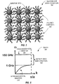
- Fig. 3 illustrates an embodiment of a top view of a portion of the QD array structure 104 described with reference to Fig. 1 .
- the PVD 102 is disposed within a body or hull 202 of the airship 100.
- the QD array structure 104 included in the PVD 102 is disposed between the pair of electrodes 106.
- a rectifying antenna 210 device is operable to convert the electromagnetic waves (not shown) emitted by the PVD 102 as an output into a DC power output.
- An efficiency of the rectifying antenna 210 device may be configured to be at least 90 percent.
- the rectifying antenna 210 device may include a plurality of diode and dipole elements arranged in a mesh pattern to obtain directional properties.
- the rectifying antenna 210 device which may also include filter circuits, may be implemented as a thin film device. Such a thin film antenna may also be rapidly adjusted to match the desired shape, form, or size that optimizes the intended functional and frequency requirements.
- the quantum dot (QD) array structure 104 includes a plurality of sheet layers of quantum dots arranged in a matrix structure.
- the quantum dots have a configurable diameter and are spaced apart at a configurable center-to-center distance between adjacent QD's.
- the sheet layer thickness and sheet layer length is also configurable.
- a QD is a light absorbing semiconducting crystal approximately 1-100 nanometers in diameter.
- the QD confines the motion of conduction band electrons and valence band holes in all three spatial directions by the potential energy barriers that form the QD's boundaries.
- a structured array of QD's or nanocrystals is embedded in a supporting matrix of conductive polymer composite material 310 to form the PVD 102.
- the QD array structure 104 can be fabricated through self-assembly or through templated growth.
- the PVD 102 is operable to convert incident heat energy having wavelengths ranging from approximately 8 microns to approximately 40 microns into electromagnetic waves having frequencies at or above the X-band portion of the frequency spectrum (corresponding to wavelengths of about 30 millimeters to about 30 micrometers).
- the PVD 102 can be tuned to absorb incident photons having different wavelengths, e.g., photons between approximately 8 microns to approximately 12 microns emitted by energy sources below approximately 600 degrees Celsius, by varying the size and separation between QD's and by selecting the material used to fabricate the QD's.
- a frequency of the electromagnetic waves emitted by the PVD 102 as an output is tunable in dependence of strength of an electric field applied. Additional detail of the energy and wavelength conversion feature of the PVD 102 is described with reference to Fig. 4 .
- Fig. 4 illustrates an embodiment of an energy band gap 400 associated with a quantum dot described with reference to Fig. 1, Fig. 2 and Fig. 3 .
- the band gap for bulk semiconductors separates the valence band from the more energetic conduction band, making it difficult for electrons to jump to the conduction band.
- the band gap is fixed (e.g., about 0.1 electron volt (eV) to 1.0 eV for most semiconductors) owing to continuous energy states.
- the band gap 400 is present in discrete energy states (C1 410 , C2 420 , C3 430 in the conduction band, and V1 412 , V2 422 , V3 432 in the valence band) and is dependent on the size of the nanocrystal.
- the band gap 400 may be altered to produce a range of discrete energy states between the valence and conduction band. For example, the addition or subtraction of one atom or electron to the nanocrystal measurably changes the energy of the band gap.
- the incident photons 108 are absorbed by a quantum dot causing at least one electron 440 to be excited.
- a corresponding hole (or absence of electron) 442 is also generated in the valence band.
- the electron 440 and the hole 442 may be individually or collectively referred to as a charge carrier.
- the combination of the electron 440 and the hole 442 is referred as an exciton.
- the absorbed energy enables the electron 440 to cross the band gap from V1 412 discrete energy state to C1 410 discrete energy state provided the amount of energy absorbed is sufficient to cross the band gap.
- adjacent discrete energy states have a decreasing energy level, e.g., C1 410 > C2 420 > C3 430 .
- the electron 440 and the hole 442 travel in opposing directions towards the respective electrode.
- the downward slope for the band gap is zero.
- a transition occurs from C1 410 to the C2 420 discrete energy state, and then from C2 420 to the C3 4 30 discrete energy state. Each one of the transitions of the electron 440 causes an emitted photon 450 to be generated.
- a transition occurs from V3 432 to the V2 422 discrete energy state, and then from V2 422 to the V1 412 discrete energy state. Each one of the transitions of the hole 442 causes another emitted photon to be generated.
- a number of the emitted photons are greater than a number of the incident photons by a factor of at least 2X (one each for electron and hole transition).
- each electron crossing the band gap 400 is capable of generating multiple ones of the emitted photon 450 depending on a number of transitions between the discrete energy states, thereby improving the gain and the efficiency of the PVD 102.
- the charge carriers are harvested as the emitted photons before the charge carriers are captured by the electrodes 106.
- no energy is harvested from the electric field for generating multiple ones of the emitted photon 450. The electric field is only used to reduce the band gap over which the electron 440 must jump to get into the conduction band. Thus, the electric field is not depleted or diminished in the wavelength conversion process.
- Equation 100 defines a relationship between a frequency of the emitted electromagnetic wave and the bias voltage.
- f_out is the output photon frequency
- h Planck's constant
- e is the electron charge
- V_bias is the bias voltage
- d is the center-to-center spacing of the nanocrystals (measured in the direction parallel to the applied electric field)
- L is the total length of the sample. The equation assumes that there is no built-in field arising from a graded impurity concentration in the supporting matrix of conductive polymer composite material 310 or substrate (as in a semiconductor p-n junction).
- multiple ones of the emitted photon 450 are emitted or radiated as an electromagnetic wave having a frequency at or above the X-band portion of the frequency spectrum (ranging from about 10 GHz to about 1 THz), which corresponds to wavelength of about 30 millimeters to about 30 micrometers.
- the frequency of the output electromagnetic wave may be configured to be at least 1 THz but less than 10 THz.
- the QD array structure 104 of the PVD 102 is tuned to absorb infrared photons by generating a gap in the phonon band structure.
- a phonon is a quantized mode of vibration occurring in a nanocrystal lattice structure, e.g., the QD array structure 104 of the PVD 102. Additional details of the gap in the phonon band structure for passing the desired frequencies, e.g., at or above the X-band, are described with reference to Fig. 5 .
- the DC power required for on-board equipment may be generated by the rectifying antenna 210. Therefore, the process to generate the DC current is free from the need to collect and physically transport the charge carriers to the electrodes to generate the DC current.
- the PVD 102 achieves energy and wavelength conversion before the charge carriers reach the electrodes 106.
- the output voltage of the PVD 102 is determined by how the emitted photons are used and not limited by the energy of the incident photons.
- Fig. 5 illustrates a frequency response graph 500 for vibrations occurring in the QD array structure 104 of the PVD 102 described with reference to Fig. 1, Fig. 2 , Fig. 3 , and Fig. 4 , according to an embodiment.
- the QD array structure 104 vibrates in response to the incident photons 108 , the vibrations being in accordance with a phonon band structure for the QD array structure 104.
- the phonon band structure is configurable to suppress the transition that causes energy loss due to the vibrations instead of harvesting energy as the emitted photons.
- the phonon band structure includes a gap at the configurable frequency (or a configurable range of frequencies) of the electromagnetic wave output.
- the phonon gap opened up by the QD array structure 104 of the PVD 102 increases the lifetime of the excited states and enables multiple GHz/THz photons to be emitted for each incident photon.
- the bulk acoustic phonons are split into two groups: the low frequency group (illustrated by Y-axis of the graph 500 ) that results in an overall translation of the nanocrystal (nanocrystal "acoustic" phonons), and a higher frequency group (not shown) that includes vibrations within the nanocrystal (nanocrystal "optical” phonons).
- the bulk optical phonons are still active, but lie much higher in frequency (10's of THz instead of GHz).
- the absorption of incident photons 108 on the QD's causes the QD's to generate an inter-nanocrystal vibration 510 having a frequency less than approximately 1 GHz and an intra-nanocrystal vibration 520 having a frequency equal to 150 GHz.
- a gap 530 in the phonon band structure e.g., between 1 GHz and 150 GHz, is beneficial to photon emission when the charge carriers transition and travel between nanocrystals because there are no non-radiative channels in which to dissipate energy.
- the gap 530 in the phonon band structure is achieved due to confinement of bulk acoustic phonons in the nanocrystal geometry, and the soft conductive polymer composite material 310 in which the nanocrystals are embedded.
- the nanocrystals are effectively zero-dimensional, there is no need for phonon emission to accompany photon emission to conserve momentum. Since the phonon band gap is readily achieved in close-packed nanocrystal colloidal crystals, there is no conflict between phonon band gap formation and charge carrier movement. Absorbed infrared radiation is down-converted and re-emitted as electromagnetic wave (GHz/THz) radiation instead of being absorbed by the nanocrystals and converted into heat (phonons).
- GHz/THz electromagnetic wave
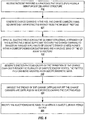
- Fig. 6 is a flow chart of a method for harvesting energy from incident photons. The method is used to harvest energy from incident photons using the PVD 102 described with reference to Fig.'s 1, 2, 3, 4 and 5.
- incident photons are received by a photovoltaic device (PVD) having a quantum dot (QD) array structure.
- QD quantum dot
- charge carriers are generated in the PVD by harvesting the energy from the incident photons.
- an electric field is applied across the QD array structure. Strength of the electric field is sufficient to cause the charge carriers to transition through a plurality of discrete energy states formed within a corresponding conductive band and a valence band of the QD array structure.
- emitted photons are generated.
- the emitted photons are caused by the transition of the charge carriers through the plurality of discrete energy states.
- the emitted photons are radiated as an electromagnetic wave having a tunable wavelength and frequency.
- harvesting of the energy contained within the charge carriers is completed before the charge carriers are captured by the electrodes.
- the electromagnetic wave radiated as an output is rectified to generate a DC power output.
- Embodiments disclosed herein provide an efficient nanocrystal structure based photovoltaic device that is operable to harvest energy from infrared sources (operating below 600 degrees Celsius) and emit electromagnetic radiation waves having tunable frequencies at or above the X-band portion of the frequency spectrum (ranging from about 10 GHz to about 1 THz).
- the electromagnetic radiation waves are captured and rectified into a DC current by using rectenna structures.
- the process to generate the DC current is free from the need to collect and physically transport the charge carriers to generate DC current.
- the output voltage of the apparatus is not limited by the energy of the incident photons, thereby enabling the harvesting of electric power generation from heat sources below degrees Celsius.
- the illustrative embodiments presented herein provide a simple, reliable, sustainable, and efficient energy conversion apparatus and method that is suitable for use in an aerospace environment.
Landscapes
- Engineering & Computer Science (AREA)
- Aviation & Aerospace Engineering (AREA)
- Life Sciences & Earth Sciences (AREA)
- Sustainable Development (AREA)
- Remote Sensing (AREA)
- Mechanical Engineering (AREA)
- Chemical & Material Sciences (AREA)
- Combustion & Propulsion (AREA)
- Photovoltaic Devices (AREA)
Claims (13)
- Vorrichtung, umfassend:eine photovoltaische Einrichtung mit einer Quantenpunkt-(QD)-Array-Struktur, die dazu ausgelegt ist, Ladungsträger aus einfallenden Photonen zu erzeugen; undeinen elektrischen Feldgenerator, der ein Elektrodenpaar umfasst, wobei die QD-Array-Struktur zwischen den beiden Elektroden angeordnet ist, wobei der elektrische Feldgenerator dazu ausgelegt ist, eine Vorspannung an die QD-Array-Struktur über das Elektrodenpaar anzulegen, um zu bewirken, dass die Ladungsträger eine Vielzahl von diskreten Energiezuständen durchlaufen, die sich innerhalb eines entsprechenden leitenden Bandes oder eines Valenzbandes der QD-Array-Struktur einstellen, und die QD-Array-Struktur dazu ausgelegt ist, eine Anzahl an emittierten Photonen zu erzeugen, die basierend auf jedem Übergang zwischen der Vielzahl von diskreten Energiezuständen um einen Faktor von mindestens 2 größer als eine Anzahl der einfallenden Photonen ist; undeine Gleichrichtantenne, die betreibbar ist, um einen Gleichstrom aus den emittierten Photonen zu erzeugen, wobei die Gleichrichtantenne in direktem physischen Kontakt mit einer oberen Elektrode des Elektrodenpaares steht.
- Vorrichtung nach Anspruch 1, wobei:
eine konfigurierbare Wellenlänge der emittierten Photonen auf der angelegten Vorspannung beruht. - Vorrichtung nach einem der vorhergehenden Ansprüche, wobei der Übergang eines Ladungsträgers von einem diskreten Energiezustand zu einem benachbarten diskreten Energiezustand ein emittiertes Photon erzeugt.
- Vorrichtung nach einem der vorhergehenden Ansprüche, wobei Energie in den Ladungsträgern in Form der emittierten Photonen gewonnen wird, bevor die Ladungsträger von einer oder mehreren der beiden Elektroden des elektrischen Feldgenerators eingefangen werden.
- Vorrichtung nach einem der vorhergehenden Ansprüche, wobei jeder der Vielzahl von Quantenpunkten einen konfigurierbaren Durchmesser aufweist, wobei die Vielzahl von Quantenpunkten in einer Schichtlage mit konfigurierbarer Dicke und konfigurierbarer Länge angeordnet sind.
- Vorrichtung nach einem der vorhergehenden Ansprüche, wobei die einfallenden Photonen eine Wellenlänge in einem konfigurierbaren Bereich zwischen ca. 8 Mikron und ca. 40 Mikron aufweisen.
- Vorrichtung nach einem der vorhergehenden Ansprüche, wobei jedes der emittierten Photonen als elektromagnetische Welle mit einer konfigurierbaren Frequenz emittiert wird.
- Vorrichtung nach Anspruch 7, wobei die konfigurierbare Frequenz in Abhängigkeit von mindestens einem der folgenden Parameter abstimmbar ist: eine Größe eines Quantenpunktes, der in der QD-Array-Struktur enthalten ist, ein Abstand zwischen benachbarten Quantenpunkten, die in der QD-Array-Struktur enthalten sind, eine Dicke der QD-Array-Struktur, die als Schicht gebildet ist, eine Länge der Schicht und eine Spannung des elektrischen Feldes.
- Vorrichtung nach Anspruch 7 oder Anspruch 8, wobei die konfigurierbare Frequenz innerhalb eines Hochfrequenzbereichs von 10 Gigahertz bis ca. 1 Terahertz liegt.
- Vorrichtung nach Anspruch 7, 8 oder 9, wobei die QD-Array-Struktur im Ansprechen auf die einfallenden Photonen vibriert, wobei die Vibrationen einer Phononenbandstruktur für die QD-Array-Struktur entsprechen, wobei die Phononenbandstruktur einen Lücke bei der konfigurierbaren Frequenz aufweist.
- Vorrichtung nach Anspruch 10, wobei anstelle der emittierten Photonen die Phononenbandstruktur konfigurierbar ist, um den Übergang zu unterbinden, der die Vibrationen verursacht.
- Vorrichtung nach einem der vorhergehenden Ansprüche, wobei die einfallenden Photonen von Wärmequellen mit einer Temperatur unter 600 Grad Celsius erzeugt werden.
- Fahrzeug, das mit der Vorrichtung nach einem der vorhergehenden Ansprüche ausgestattet ist.
Applications Claiming Priority (1)
| Application Number | Priority Date | Filing Date | Title |
|---|---|---|---|
| US12/388,699 US8759666B2 (en) | 2009-02-19 | 2009-02-19 | Wavelength conversion photovoltaics |
Publications (3)
| Publication Number | Publication Date |
|---|---|
| EP2230548A2 EP2230548A2 (de) | 2010-09-22 |
| EP2230548A3 EP2230548A3 (de) | 2013-01-30 |
| EP2230548B1 true EP2230548B1 (de) | 2019-09-11 |
Family
ID=42537859
Family Applications (1)
| Application Number | Title | Priority Date | Filing Date |
|---|---|---|---|
| EP10152422.1A Active EP2230548B1 (de) | 2009-02-19 | 2010-02-02 | Vorrichtung zur Umwandlung von einfallenden Photonen zu Gleichstrom |
Country Status (2)
| Country | Link |
|---|---|
| US (1) | US8759666B2 (de) |
| EP (1) | EP2230548B1 (de) |
Families Citing this family (9)
| Publication number | Priority date | Publication date | Assignee | Title |
|---|---|---|---|---|
| US9124213B2 (en) * | 2010-02-19 | 2015-09-01 | Qualcomm Incorporated | Method and apparatus for cooling and energy capture in an electronic device via a photovoltaics |
| US20140150860A1 (en) * | 2011-05-16 | 2014-06-05 | The Board Of Trustees Of The University Of Illinoi | Electronic device from dissipative quantum dots |
| WO2012162268A2 (en) * | 2011-05-20 | 2012-11-29 | Solexel, Inc. | Self-activated front surface bias for a solar cell |
| EP2710639A4 (de) | 2011-05-20 | 2015-11-25 | Solexel Inc | Selbstaktivierte vorderseiten-vorspannung für eine solarzelle |
| US20150380590A1 (en) * | 2014-06-26 | 2015-12-31 | Nxp B.V. | Energy harvester |
| US20180334090A1 (en) * | 2017-05-19 | 2018-11-22 | Ford Global Technologies, Llc | Brake component illuminator and illumination method |
| US12152988B2 (en) * | 2021-05-07 | 2024-11-26 | University Of South Carolina | Spatially resolved fourier transform impedance spectroscopy and applications to optoelectronics |
| US12500422B2 (en) * | 2024-04-10 | 2025-12-16 | Leigh M. Rothschild | Smart energy recycling system and method thereof |
| US20250350124A1 (en) * | 2024-04-10 | 2025-11-13 | Leigh M. Rothschild | Smart energy harvesting system and method thereof |
Citations (1)
| Publication number | Priority date | Publication date | Assignee | Title |
|---|---|---|---|---|
| US20050284147A1 (en) * | 2004-06-29 | 2005-12-29 | Lockheed Martin Corporation | Systems and methods for converting heat to electrical power |
Family Cites Families (7)
| Publication number | Priority date | Publication date | Assignee | Title |
|---|---|---|---|---|
| US6541788B2 (en) * | 1998-10-27 | 2003-04-01 | The Regents Of The University Of California | Mid infrared and near infrared light upconverter using self-assembled quantum dots |
| US7371962B2 (en) * | 1999-05-04 | 2008-05-13 | Neokismet, Llc | Diode energy converter for chemical kinetic electron energy transfer |
| US6882128B1 (en) * | 2000-09-27 | 2005-04-19 | Science Applications International Corporation | Method and system for energy reclamation and reuse |
| US7271405B2 (en) * | 2003-10-14 | 2007-09-18 | Stc.Unm | Intersubband detector with avalanche multiplier region |
| KR100682928B1 (ko) * | 2005-02-03 | 2007-02-15 | 삼성전자주식회사 | 양자점 화합물을 포함하는 에너지 변환막 및 양자점 박막 |
| DE102005018820A1 (de) | 2005-04-22 | 2006-11-02 | Universität Augsburg | Akustisch gesteuerte und gespeiste Lichtquelle unter Verwendung von akusto-optisch angeregten Intrabandübergängen |
| US20080230782A1 (en) * | 2006-10-09 | 2008-09-25 | Homer Antoniadis | Photoconductive devices with enhanced efficiency from group iv nanoparticle materials and methods thereof |
-
2009
- 2009-02-19 US US12/388,699 patent/US8759666B2/en active Active
-
2010
- 2010-02-02 EP EP10152422.1A patent/EP2230548B1/de active Active
Patent Citations (1)
| Publication number | Priority date | Publication date | Assignee | Title |
|---|---|---|---|---|
| US20050284147A1 (en) * | 2004-06-29 | 2005-12-29 | Lockheed Martin Corporation | Systems and methods for converting heat to electrical power |
Also Published As
| Publication number | Publication date |
|---|---|
| EP2230548A2 (de) | 2010-09-22 |
| US20100206359A1 (en) | 2010-08-19 |
| US8759666B2 (en) | 2014-06-24 |
| EP2230548A3 (de) | 2013-01-30 |
Similar Documents
| Publication | Publication Date | Title |
|---|---|---|
| EP2230548B1 (de) | Vorrichtung zur Umwandlung von einfallenden Photonen zu Gleichstrom | |
| US8529825B2 (en) | Fabrication of nanovoid-imbedded bismuth telluride with low dimensional system | |
| US7750425B2 (en) | Intermediate-band photosensitive device with quantum dots embedded in energy fence barrier | |
| US8969710B2 (en) | Photon induced enhanced field electron emission collector | |
| US8736108B1 (en) | Photovoltaic system | |
| KR101596972B1 (ko) | 유형 ⅱ 양자점 태양전지 | |
| JP5783332B2 (ja) | 複合粒子、複合粒子分散体、及び、光起電装置 | |
| US9117954B2 (en) | High efficiency nanostructured photovoltaic device manufacturing | |
| US20110023941A1 (en) | Ultra-efficient energy conversion device for converting light to electricity by rectifying surface plasmon polaritons | |
| US7446451B2 (en) | Systems and methods for converting heat to electrical power | |
| US20250096613A1 (en) | Space-based solar energy harvesting | |
| KR20090054260A (ko) | 태양전지 | |
| WO2013089554A1 (en) | A light receiving and emitting device and method of producing thereof | |
| WO2009085089A9 (en) | Fabrication of nanovoid-imbedded bismuth telluride with low dimensional system | |
| US9741882B2 (en) | Tandem junction photovoltaic cell | |
| JP2016225546A (ja) | 光電変換素子 | |
| Lu et al. | Photocurrent Spectroscopy | |
| Bishnoi | Quantum dots: Rethinking the electronics | |
| JP2015079870A (ja) | 太陽電池 | |
| Potdar | Nanophotovoltaic and energy harvesting | |
| Saurov | Power calculation of GaN/AlGaN based thermo-photovoltaic heterostructure | |
| Lester et al. | Solar power for unmanned autonomous vehicles | |
| Mishra et al. | Witricity Transmission by Satellites using carbon nanotubic solar cells |
Legal Events
| Date | Code | Title | Description |
|---|---|---|---|
| PUAI | Public reference made under article 153(3) epc to a published international application that has entered the european phase |
Free format text: ORIGINAL CODE: 0009012 |
|
| AK | Designated contracting states |
Kind code of ref document: A2 Designated state(s): AT BE BG CH CY CZ DE DK EE ES FI FR GB GR HR HU IE IS IT LI LT LU LV MC MK MT NL NO PL PT RO SE SI SK SM TR |
|
| AX | Request for extension of the european patent |
Extension state: AL BA RS |
|
| PUAL | Search report despatched |
Free format text: ORIGINAL CODE: 0009013 |
|
| AK | Designated contracting states |
Kind code of ref document: A3 Designated state(s): AT BE BG CH CY CZ DE DK EE ES FI FR GB GR HR HU IE IS IT LI LT LU LV MC MK MT NL NO PL PT RO SE SI SK SM TR |
|
| AX | Request for extension of the european patent |
Extension state: AL BA RS |
|
| RIC1 | Information provided on ipc code assigned before grant |
Ipc: B64G 1/22 20060101ALI20121221BHEP Ipc: B64G 1/44 20060101ALI20121221BHEP Ipc: H01L 31/04 20060101ALI20121221BHEP Ipc: G02F 1/00 20060101AFI20121221BHEP |
|
| 17P | Request for examination filed |
Effective date: 20130726 |
|
| RBV | Designated contracting states (corrected) |
Designated state(s): AT BE BG CH CY CZ DE DK EE ES FI FR GB GR HR HU IE IS IT LI LT LU LV MC MK MT NL NO PL PT RO SE SI SK SM TR |
|
| 17Q | First examination report despatched |
Effective date: 20160119 |
|
| REG | Reference to a national code |
Ref country code: DE Ref legal event code: R079 Ref document number: 602010060965 Country of ref document: DE Free format text: PREVIOUS MAIN CLASS: G02F0001000000 Ipc: H01L0031040000 |
|
| RIC1 | Information provided on ipc code assigned before grant |
Ipc: H01L 31/04 20140101AFI20190129BHEP Ipc: B64G 1/44 20060101ALI20190129BHEP |
|
| GRAP | Despatch of communication of intention to grant a patent |
Free format text: ORIGINAL CODE: EPIDOSNIGR1 |
|
| STAA | Information on the status of an ep patent application or granted ep patent |
Free format text: STATUS: GRANT OF PATENT IS INTENDED |
|
| INTG | Intention to grant announced |
Effective date: 20190322 |
|
| GRAS | Grant fee paid |
Free format text: ORIGINAL CODE: EPIDOSNIGR3 |
|
| GRAA | (expected) grant |
Free format text: ORIGINAL CODE: 0009210 |
|
| STAA | Information on the status of an ep patent application or granted ep patent |
Free format text: STATUS: THE PATENT HAS BEEN GRANTED |
|
| AK | Designated contracting states |
Kind code of ref document: B1 Designated state(s): AT BE BG CH CY CZ DE DK EE ES FI FR GB GR HR HU IE IS IT LI LT LU LV MC MK MT NL NO PL PT RO SE SI SK SM TR |
|
| REG | Reference to a national code |
Ref country code: GB Ref legal event code: FG4D |
|
| REG | Reference to a national code |
Ref country code: CH Ref legal event code: EP |
|
| REG | Reference to a national code |
Ref country code: AT Ref legal event code: REF Ref document number: 1179598 Country of ref document: AT Kind code of ref document: T Effective date: 20190915 |
|
| REG | Reference to a national code |
Ref country code: DE Ref legal event code: R096 Ref document number: 602010060965 Country of ref document: DE Ref country code: IE Ref legal event code: FG4D |
|
| REG | Reference to a national code |
Ref country code: NL Ref legal event code: MP Effective date: 20190911 |
|
| REG | Reference to a national code |
Ref country code: LT Ref legal event code: MG4D |
|
| PG25 | Lapsed in a contracting state [announced via postgrant information from national office to epo] |
Ref country code: FI Free format text: LAPSE BECAUSE OF FAILURE TO SUBMIT A TRANSLATION OF THE DESCRIPTION OR TO PAY THE FEE WITHIN THE PRESCRIBED TIME-LIMIT Effective date: 20190911 Ref country code: LT Free format text: LAPSE BECAUSE OF FAILURE TO SUBMIT A TRANSLATION OF THE DESCRIPTION OR TO PAY THE FEE WITHIN THE PRESCRIBED TIME-LIMIT Effective date: 20190911 Ref country code: BG Free format text: LAPSE BECAUSE OF FAILURE TO SUBMIT A TRANSLATION OF THE DESCRIPTION OR TO PAY THE FEE WITHIN THE PRESCRIBED TIME-LIMIT Effective date: 20191211 Ref country code: NO Free format text: LAPSE BECAUSE OF FAILURE TO SUBMIT A TRANSLATION OF THE DESCRIPTION OR TO PAY THE FEE WITHIN THE PRESCRIBED TIME-LIMIT Effective date: 20191211 Ref country code: SE Free format text: LAPSE BECAUSE OF FAILURE TO SUBMIT A TRANSLATION OF THE DESCRIPTION OR TO PAY THE FEE WITHIN THE PRESCRIBED TIME-LIMIT Effective date: 20190911 Ref country code: HR Free format text: LAPSE BECAUSE OF FAILURE TO SUBMIT A TRANSLATION OF THE DESCRIPTION OR TO PAY THE FEE WITHIN THE PRESCRIBED TIME-LIMIT Effective date: 20190911 |
|
| PG25 | Lapsed in a contracting state [announced via postgrant information from national office to epo] |
Ref country code: LV Free format text: LAPSE BECAUSE OF FAILURE TO SUBMIT A TRANSLATION OF THE DESCRIPTION OR TO PAY THE FEE WITHIN THE PRESCRIBED TIME-LIMIT Effective date: 20190911 Ref country code: GR Free format text: LAPSE BECAUSE OF FAILURE TO SUBMIT A TRANSLATION OF THE DESCRIPTION OR TO PAY THE FEE WITHIN THE PRESCRIBED TIME-LIMIT Effective date: 20191212 Ref country code: ES Free format text: LAPSE BECAUSE OF FAILURE TO SUBMIT A TRANSLATION OF THE DESCRIPTION OR TO PAY THE FEE WITHIN THE PRESCRIBED TIME-LIMIT Effective date: 20190911 |
|
| REG | Reference to a national code |
Ref country code: AT Ref legal event code: MK05 Ref document number: 1179598 Country of ref document: AT Kind code of ref document: T Effective date: 20190911 |
|
| PG25 | Lapsed in a contracting state [announced via postgrant information from national office to epo] |
Ref country code: NL Free format text: LAPSE BECAUSE OF FAILURE TO SUBMIT A TRANSLATION OF THE DESCRIPTION OR TO PAY THE FEE WITHIN THE PRESCRIBED TIME-LIMIT Effective date: 20190911 Ref country code: AT Free format text: LAPSE BECAUSE OF FAILURE TO SUBMIT A TRANSLATION OF THE DESCRIPTION OR TO PAY THE FEE WITHIN THE PRESCRIBED TIME-LIMIT Effective date: 20190911 Ref country code: PL Free format text: LAPSE BECAUSE OF FAILURE TO SUBMIT A TRANSLATION OF THE DESCRIPTION OR TO PAY THE FEE WITHIN THE PRESCRIBED TIME-LIMIT Effective date: 20190911 Ref country code: EE Free format text: LAPSE BECAUSE OF FAILURE TO SUBMIT A TRANSLATION OF THE DESCRIPTION OR TO PAY THE FEE WITHIN THE PRESCRIBED TIME-LIMIT Effective date: 20190911 Ref country code: PT Free format text: LAPSE BECAUSE OF FAILURE TO SUBMIT A TRANSLATION OF THE DESCRIPTION OR TO PAY THE FEE WITHIN THE PRESCRIBED TIME-LIMIT Effective date: 20200113 Ref country code: RO Free format text: LAPSE BECAUSE OF FAILURE TO SUBMIT A TRANSLATION OF THE DESCRIPTION OR TO PAY THE FEE WITHIN THE PRESCRIBED TIME-LIMIT Effective date: 20190911 |
|
| PG25 | Lapsed in a contracting state [announced via postgrant information from national office to epo] |
Ref country code: SM Free format text: LAPSE BECAUSE OF FAILURE TO SUBMIT A TRANSLATION OF THE DESCRIPTION OR TO PAY THE FEE WITHIN THE PRESCRIBED TIME-LIMIT Effective date: 20190911 Ref country code: IS Free format text: LAPSE BECAUSE OF FAILURE TO SUBMIT A TRANSLATION OF THE DESCRIPTION OR TO PAY THE FEE WITHIN THE PRESCRIBED TIME-LIMIT Effective date: 20200224 Ref country code: CZ Free format text: LAPSE BECAUSE OF FAILURE TO SUBMIT A TRANSLATION OF THE DESCRIPTION OR TO PAY THE FEE WITHIN THE PRESCRIBED TIME-LIMIT Effective date: 20190911 Ref country code: SK Free format text: LAPSE BECAUSE OF FAILURE TO SUBMIT A TRANSLATION OF THE DESCRIPTION OR TO PAY THE FEE WITHIN THE PRESCRIBED TIME-LIMIT Effective date: 20190911 |
|
| REG | Reference to a national code |
Ref country code: DE Ref legal event code: R097 Ref document number: 602010060965 Country of ref document: DE |
|
| PLBE | No opposition filed within time limit |
Free format text: ORIGINAL CODE: 0009261 |
|
| STAA | Information on the status of an ep patent application or granted ep patent |
Free format text: STATUS: NO OPPOSITION FILED WITHIN TIME LIMIT |
|
| PG2D | Information on lapse in contracting state deleted |
Ref country code: IS |
|
| PG25 | Lapsed in a contracting state [announced via postgrant information from national office to epo] |
Ref country code: DK Free format text: LAPSE BECAUSE OF FAILURE TO SUBMIT A TRANSLATION OF THE DESCRIPTION OR TO PAY THE FEE WITHIN THE PRESCRIBED TIME-LIMIT Effective date: 20190911 Ref country code: IS Free format text: LAPSE BECAUSE OF FAILURE TO SUBMIT A TRANSLATION OF THE DESCRIPTION OR TO PAY THE FEE WITHIN THE PRESCRIBED TIME-LIMIT Effective date: 20200112 |
|
| 26N | No opposition filed |
Effective date: 20200615 |
|
| PG25 | Lapsed in a contracting state [announced via postgrant information from national office to epo] |
Ref country code: SI Free format text: LAPSE BECAUSE OF FAILURE TO SUBMIT A TRANSLATION OF THE DESCRIPTION OR TO PAY THE FEE WITHIN THE PRESCRIBED TIME-LIMIT Effective date: 20190911 |
|
| REG | Reference to a national code |
Ref country code: CH Ref legal event code: PL |
|
| REG | Reference to a national code |
Ref country code: BE Ref legal event code: MM Effective date: 20200229 |
|
| PG25 | Lapsed in a contracting state [announced via postgrant information from national office to epo] |
Ref country code: MC Free format text: LAPSE BECAUSE OF FAILURE TO SUBMIT A TRANSLATION OF THE DESCRIPTION OR TO PAY THE FEE WITHIN THE PRESCRIBED TIME-LIMIT Effective date: 20190911 Ref country code: LU Free format text: LAPSE BECAUSE OF NON-PAYMENT OF DUE FEES Effective date: 20200202 |
|
| PG25 | Lapsed in a contracting state [announced via postgrant information from national office to epo] |
Ref country code: LI Free format text: LAPSE BECAUSE OF NON-PAYMENT OF DUE FEES Effective date: 20200229 Ref country code: CH Free format text: LAPSE BECAUSE OF NON-PAYMENT OF DUE FEES Effective date: 20200229 |
|
| PG25 | Lapsed in a contracting state [announced via postgrant information from national office to epo] |
Ref country code: IE Free format text: LAPSE BECAUSE OF NON-PAYMENT OF DUE FEES Effective date: 20200202 |
|
| PG25 | Lapsed in a contracting state [announced via postgrant information from national office to epo] |
Ref country code: BE Free format text: LAPSE BECAUSE OF NON-PAYMENT OF DUE FEES Effective date: 20200229 |
|
| PG25 | Lapsed in a contracting state [announced via postgrant information from national office to epo] |
Ref country code: TR Free format text: LAPSE BECAUSE OF FAILURE TO SUBMIT A TRANSLATION OF THE DESCRIPTION OR TO PAY THE FEE WITHIN THE PRESCRIBED TIME-LIMIT Effective date: 20190911 Ref country code: MT Free format text: LAPSE BECAUSE OF FAILURE TO SUBMIT A TRANSLATION OF THE DESCRIPTION OR TO PAY THE FEE WITHIN THE PRESCRIBED TIME-LIMIT Effective date: 20190911 Ref country code: CY Free format text: LAPSE BECAUSE OF FAILURE TO SUBMIT A TRANSLATION OF THE DESCRIPTION OR TO PAY THE FEE WITHIN THE PRESCRIBED TIME-LIMIT Effective date: 20190911 |
|
| PG25 | Lapsed in a contracting state [announced via postgrant information from national office to epo] |
Ref country code: MK Free format text: LAPSE BECAUSE OF FAILURE TO SUBMIT A TRANSLATION OF THE DESCRIPTION OR TO PAY THE FEE WITHIN THE PRESCRIBED TIME-LIMIT Effective date: 20190911 |
|
| REG | Reference to a national code |
Ref country code: DE Ref legal event code: R079 Ref document number: 602010060965 Country of ref document: DE Free format text: PREVIOUS MAIN CLASS: H01L0031040000 Ipc: H10F0010000000 |
|
| PGFP | Annual fee paid to national office [announced via postgrant information from national office to epo] |
Ref country code: GB Payment date: 20260227 Year of fee payment: 17 |
|
| PGFP | Annual fee paid to national office [announced via postgrant information from national office to epo] |
Ref country code: DE Payment date: 20260227 Year of fee payment: 17 |
|
| PGFP | Annual fee paid to national office [announced via postgrant information from national office to epo] |
Ref country code: IT Payment date: 20260219 Year of fee payment: 17 |
|
| PGFP | Annual fee paid to national office [announced via postgrant information from national office to epo] |
Ref country code: FR Payment date: 20260225 Year of fee payment: 17 |