EP2228836A2 - Light emitting device - Google Patents
Light emitting device Download PDFInfo
- Publication number
- EP2228836A2 EP2228836A2 EP09176705A EP09176705A EP2228836A2 EP 2228836 A2 EP2228836 A2 EP 2228836A2 EP 09176705 A EP09176705 A EP 09176705A EP 09176705 A EP09176705 A EP 09176705A EP 2228836 A2 EP2228836 A2 EP 2228836A2
- Authority
- EP
- European Patent Office
- Prior art keywords
- layer
- light emitting
- emitting device
- shape
- semiconductor layer
- Prior art date
- Legal status (The legal status is an assumption and is not a legal conclusion. Google has not performed a legal analysis and makes no representation as to the accuracy of the status listed.)
- Granted
Links
Images



Classifications
-
- H—ELECTRICITY
- H10—SEMICONDUCTOR DEVICES; ELECTRIC SOLID-STATE DEVICES NOT OTHERWISE PROVIDED FOR
- H10H—INORGANIC LIGHT-EMITTING SEMICONDUCTOR DEVICES HAVING POTENTIAL BARRIERS
- H10H20/00—Individual inorganic light-emitting semiconductor devices having potential barriers, e.g. light-emitting diodes [LED]
- H10H20/80—Constructional details
- H10H20/81—Bodies
- H10H20/819—Bodies characterised by their shape, e.g. curved or truncated substrates
-
- H—ELECTRICITY
- H10—SEMICONDUCTOR DEVICES; ELECTRIC SOLID-STATE DEVICES NOT OTHERWISE PROVIDED FOR
- H10H—INORGANIC LIGHT-EMITTING SEMICONDUCTOR DEVICES HAVING POTENTIAL BARRIERS
- H10H20/00—Individual inorganic light-emitting semiconductor devices having potential barriers, e.g. light-emitting diodes [LED]
- H10H20/80—Constructional details
- H10H20/83—Electrodes
- H10H20/831—Electrodes characterised by their shape
Definitions
- This relates to a light emitting device.
- a light emitting diode is a semiconductor light emitting device that converts current to light.
- the wavelength of light emitted by such an LED depends on a band-gap of the semiconductor material used in the LED, the band gap representing an energy difference between a valence band and a conduction band.
- LEDs have been used as a light source for displays such as liquid crystal displays (LCDs), a light source for automobiles, and a light source for other types of lighting devices.
- An LED may emit white light by using phosphor materials or may emit various colors by combining LEDs having various colors.
- the efficiency of the LEDs may be significantly degraded.
- An LCD apparatus may produce various colors by controlling polarization of the light source.
- the light emitted by the light source may pass through a polarizer, so that the light passing through the polarizer has polarizing components in a specific direction.
- a vertical type light emitting device including a light emitting semiconductor layer including a first conductive type semiconductor layer, an active layer and a second conductive type semiconductor layer, a first electrode layer disposed on the light emitting semiconductor layer and a second electrode layer disposed under the light emitting semiconductor layer.
- Light emitting efficiency of a vertical type light emitting device may be increased when a reflective layer having a relatively high reflectance is formed between the second conductive type semiconductor layer and the second electrode layer
- the distance between the active layer and the reflective layer may be relatively close so that the distance between the active layer and the reflective layer is less than the wavelength of the light emitted from the active layer.
- a quantum interference effect may be generated so that the optical characteristics of the light emitting device may be changed. For example, as the distance between the active layer and the reflective layer is changed, a damping rate of a dipole source of the light emitted from the light emitting device may be changed.
- FIGS. 1 and 2 illustrate the change in damping rate according to the vibration direction of the dipole source of light emitted from a light emitting device according to the change in distance between an active layer and a reflective layer.
- the damping rate refers to a turnaround time in the light emitting device from the time at which electrons receive energy until the time at which the energy is emitted in the form of light.
- dipole source light emission is increased so that internal quantum efficiency may be improved.
- the damping rate of the light emitted from the light emitting device is changed in relation to the gap distance D between the active layer and the reflective layer, the refractive index of material that forms the light emitting device, and the wavelength emitted from the light emitting device.
- the Y axis represents the damping rate
- the lower X axis represents the distance D between the active layer and the reflective layer
- the upper X axis represents the relative value obtained by dividing the distance D between the active layer and the reflective layer by ⁇ /n in which, ⁇ represents the peak wavelength of the light emitted from the light emitting device, and n represents the refractive index of material that forms the light emitting device.
- the damping rate according to the vibration direction of the dipole source of the light emitted from the light emitting device is changed as the distance D between the active layer and the reflective layer is changed.
- the damping rate is increased as the distance between the active layer and the reflective layer becomes shorter.
- the maximum value of the damping rate is shown at a specific distance (for example, 50nm).
- the distance between the active layer and the reflective layer is shorter than the wavelength of the light emitted from the light emitting device, so optical characteristics can be changed according to the change in the distance D between the active layer and the reflective layer.
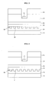
- FIG. 3 illustrates a light emitting device according to a first embodiment as broadly described herein.
- the light emitting device includes a first electrode layer 10, a reflective layer 20 formed on the first electrode layer 10, patterned layers 80 formed on the reflective layer 20, a first conductive type semiconductor layer 30 formed on the reflective layer 20 and the patterned layers 80, an active layer 40 formed on the first conductive type semiconductor layer 30, a second conductive type semiconductor layer 50 formed on the active layer 40, and a second electrode layer 70 formed on the second conductive type semiconductor layer 50.
- a non-conductive semiconductor layer 60 may be selectively formed on the second conductive type semiconductor layer 50.
- the first electrode layer 10 which may be formed of at least one of copper (Cu), titanium (Ti), chrome (Cr), nickel (Ni), aluminum (Al), platinum (Pt), gold (Au), tungsten (W) or a semiconductor substrate implanted with impurity, is used to provide power to the active layer 40 together with the second electrode layer 70.
- the reflective layer 20 may be partially opposed to the first conductive type semiconductor layer 30 and may be formed of at least one of silver (Ag) having a high reflectance, an alloy including silver (Ag), aluminum (Al), or an alloy including aluminum (Al).
- An adhesive metal layer including nickel (Ni) or titanium (Ti) may also be formed between the first electrode layer 10 and the reflective layer 20 to reinforce interface adhesion between the second electrode layer 10 and the reflective layer 20.
- An ohmic layer (not shown in detail in Figure 3 ) that provides ohmic contact may also be formed between the reflective layer 20 and the first conductive type semiconductor layer 30.
- the patterned layer 80 is formed on an upper portion of the reflective layer 20 and under the first conductive type semiconductor layer 30.
- the side surfaces of the patterned layer 80 may be partially surrounded by the reflective layer 20.
- the reflective layer 20 may have projection parts that project upward from its upper surface, and the patterned layer 80 may be disposed between the projection parts.
- the projection parts of the reflective layer 20 and the patterned layer 80 may be at least partially disposed on the same horizontal plane.
- the patterned layer 80 and the reflective layer 20 may form a polarization induction pattern 90.
- the patterned layer 80 may be formed of a non-metal material, so that the refractive index of the patterned layer 80 is greater than the refractive index of air and is less than the refractive index of the first conductive type semiconductor layer 30.
- the patterned layer 80 may be formed as a transparent electrode and, for example, may be formed of at least any one of ITO, ZnO, GZO, RuOx or IrOx.
- the patterned layer 80 When the patterned layer 80 is formed as a transparent electrode, current may flow through the patterned layer 80 so that the patterned layer 80 may not be formed spaced apart at a predetermined interval, as shown in FIG. 3 . Rather, the patterned layer 80 may be formed on the entire region between the first conductive type semiconductor layer 30 and the reflective layer 20. In this case, a pattern that is projected in a shape similar to the patterned layer 80 may be formed on the surface opposing the reflective layer 20.
- the patterned layer 80 may be formed of dielectrics such as, for example, at least any one of SiO2, MgF2, SOG, TiO2, A1203 or Si3N4.
- dielectrics such as, for example, at least any one of SiO2, MgF2, SOG, TiO2, A1203 or Si3N4.
- the patterned layer 80 is formed of dielectrics, current does not flow through the patterned layer 80, and so the patterned layer 80 is formed of components spaced at a predetermined interval, as shown in FIG. 3 .
- the first conductive type semiconductor layer 30 and the reflective layer 20 are partially opposed to each other.
- the reflective layer 20 and the patterned layer 80 form the polarization induction pattern 90 that allows the light emitted from the light emitting device to have a polarizing component in a specific direction.
- the polarization induction pattern 90 controls the polarization of the light emitted from the active layer 40 through a symmetric pattern formed on the interface between the patterned layer 80 and the reflective layer 20.
- the polarization induction pattern 90 is disposed in a range shorter than the wavelength of the emitted light, thereby allowing light having a great quantity of polarizing components in a specific direction to be emitted by a spontaneous emission process.
- a polarization induction pattern 90 as embodied and broadly described herein, a reduction in optical efficiency to achieve a particular polarization may thus be avoided.
- the first conductive type semiconductor layer 30 may be formed of a GaN-based semiconductor layer implanted with p-type impurities
- the second conductive type semiconductor layer 50 may be formed of a GaN-based semiconductor layer implanted with n-type impurities.
- the active layer 40 which is a light emitting layer, may be formed of at least one of a single quantum well structure, a multi quantum well (MQW) structure, a quantum-wire structure, or a quantum dot structure. Other variations of Group III-IV semiconductor materials may be used.
- the non-conductive semiconductor layer 60 may be a semiconductor layer having a noticeably lower electrical conductivity compared to the second conductive type semiconductor layer 50 and the first conductive type semiconductor layer 30.
- the non-conductive semiconductor layer 60 may be an undoped GaN layer.
- the polarization induction pattern 90 includes the patterned layer 80 formed of the transparent electrode or the dielectrics between the first conductive type semiconductor layer 30 and the reflective layer 20, and the reflective layer 20 disposed on the lower surface and the side surfaces of the patterned layer 80.
- FIG. 4 illustrates a light emitting device according to another embodiment as broadly described herein.
- the light emitting device shown in FIG. 4 may include a first electrode layer 10, a reflective layer 20 formed on the first electrode layer 10, a first conductive type semiconductor layer 30 having projection patterns 31 that extend toward the reflective layer 20, an active layer 40 formed on the first conductive type semiconductor layer 30, a second conductive type semiconductor layer 50 formed on the active layer 40, and a second electrode layer 70 formed on the second conductive type semiconductor layer 50.
- a non-conductive semiconductor layer 60 may be selectively formed on the second conductive type semiconductor layer 50.
- the projection patterns 31 of the first conductive type semiconductor layer 30 and the reflective layer 20 form a polarization induction pattern 90.
- the projection patterns 31 may project towards the reflective layer 20 and be spaced at predetermined intervals such that the lower surface and the side surfaces of the projection pattern 31 are opposed to the reflective layer 20.
- the projection pattern 31 may be formed by being selectively etched after the first conductive type semiconductor layer 30 is formed or by roughening the surface of the first conductive type semiconductor layer 30 by controlling the growth condition of the first conductive type semiconductor layer 30.
- the projection pattern 31 may be formed as the GaN-based semiconductor layer so as to form patterned layer as described above.
- the polarization induction pattern 90 is formed by the projection pattern 31 of the first conductive type semiconductor layer 30 that is formed as a GaN-based semiconductor layer, and the reflective layer 20 that is a metal mirror contacting the projection pattern 31.
- FIG. 5 illustrates a light emitting device according to another embodiment as broadly described herein.
- the light emitting device shown in FIG. 5 may include a first electrode layer 10, a reflective layer 20 formed on the first electrode layer 10, patterned layers 80 formed on the reflective layer 20, a first conductive type semiconductor layer 30 formed on the reflective layer 20 and the patterned layers 80, an active layer 40 formed on the first conductive type semiconductor layer 30, a second conductive type semiconductor layer 50 formed on the active layer 40, a second electrode layer 70 formed on the second conductive type semiconductor layer 50, and a non-conductive semiconductor layer 60 formed on the second conductive type semiconductor layer 50.
- a photonic crystal structure 100 having a pillar or a hole shape may be formed on the non-conductive semiconductor layer 60, with pillars or holes 61 disposed at predetermined intervals or in a random shape so as to improve extracting efficiency of the light emitted from the light emitting device.
- the photonic crystal structure 100 formed on the non-conductive semiconductor layer 60 shown in FIG. 5 may also be applied to the embodiment of the light emitting device shown in FIG. 4 .
- the photonic crystal structure 100 may be formed on the second conductive type semiconductor layer 50 by removing the non-conductive semiconductor layer 60. This may also be applied to the embodiment shown in FIG. 4 .
- FIGS. 6 to 8 are diagrams of polarization induction patterns in the light emitting devices according to embodiments as broadly described herein.
- the polarization induction patterns 90 are plan views illustrate the shapes of the polarization induction patterns 90 as viewed on the x-y plane, whereas the polarization induction patterns 90 shown in FIGS. 3 to 5 are shown as an elevation type view.
- the polarization induction patterns 90 shown in FIGS. 6 to 8 are exemplary in nature, and the present disclosure is not limited thereto.
- FIGS. 6 to 8 the patterned layer 80 formed on the reflective layer 20 is exemplified as described in the embodiment shown in FIG. 3 , but the present disclosure may also be applied to the case where the projection patterns 31 are formed on the reflective layer 20 as described in the embodiment shown in FIG. 4 .
- the patterned layer 80 is formed on the reflective layer 20 having components thereof partially spaced apart.
- the reflective layer 20 may be formed on the patterned layer 80 having components partially spaced apart.
- the period or width of the patterned layer 80 may be replaced by the period or width of the reflective layer 20.
- the polarization induction pattern 90 has patterned layers 80 formed on the reflective layer 20 in a line shape.
- a plurality of patterned layers 80 are formed in a line shape, spaced apart at a predetermined interval in a first direction.
- the patterned layers 80 extend in a first direction and are spaced apart at a predetermined interval along a second direction that is perpendicular to the first direction.
- the patterned layers 80 may each have a line shape that that extend in a y direction, and may be spaced apart in an x direction.
- the patterned layers 80 have periodicity in the x direction, but do not have periodicity in the y direction.
- the polarization induction pattern 90 has patterned layers 80 having different lengths in a first direction and in a second direction perpendicular to the first direction formed on the reflective layer 20.
- the length in the y direction ry is greater than the length in the x direction rx, and the patterned layer 80 may have an elliptical shape having a longer length in the y direction than in the x direction.
- the patterned layers 80 are disposed on the reflective layer 20, having a different period in a first direction than in a second direction that is perpendicular to the first direction, that is, having different intervals.
- the patterned layers 80 may have a circular shape, and the period ax in the x direction may be less than the period ay in the y direction.
- the patterned layers 80 may be disposed along the first direction and the second direction perpendicular to the first direction, may be formed in a line shape and extend in the first direction or in the second direction, or may have different periods or sizes for the first direction and the second direction.
- the pattern density of the patterned layers 80 that are disposed in a row in the first direction may be different from the pattern density of the patterned layers 80 that are disposed in a row in the second direction.
- the pattern density of the patterned layers 80 that are disposed in a row in the first direction may be identical to the pattern density of the patterned layers 80 that are spaced along the second direction at a predetermined interval to be disposed in a row in the first direction.
- the patterned layers 80 may be formed having certain regularities in the first direction and the second direction, wherein the regularity in the first direction and the regularity in the second direction may be different from each other.
- FIGs. 9 and 10 illustrate the polarization ratio of light emitted from the light emitting devices of FIGs. 3-5 having the polarization induction patterns shown in FIGs. 6-8 .
- a period a of the transparent electrode pattern 81 is set to approximately 200nm.
- the light emitting layer 111 may be provided with multiple quantum well structures MQWs, having a p-GaN layer with a thickness of approximately 60nm therebetween. And, when a dipole source that vibrates in the x direction and a dipole source that vibrates in the y direction are applied, respectively, in the simulation structure as described above and shown in FIG. 9 , total emission amount may be detected from the upper direction (z direction). The total emission amount may correspond to a spontaneous emission rate.
- the total emission amount by the dipole source that vibrates in the x direction in parallel to the direction that the transparent electrode pattern 81 extends is greater than the total emission amount by the dipole source that vibrates in the y direction by 1.8 times or more.
- Light having a large amount of polarizing components in a specific direction can be emitted from the light emitting device according to the embodiments as broadly described herein.
- FIG. 11 is a diagram explaining the period, or interval, width and height of the polarization induction pattern in the light emitting devices according to embodiments as broadly described herein
- FIG. 12 illustrates the polarization ratio according to the period of the polarization induction pattern
- FIG. 13 illustrates the polarization ratio according to the width of the polarization induction pattern
- FIG. 14 illustrates the polarization ratio according to the thickness of the first conductive type semiconductor layer of the polarization induction pattern.
- the period a in the polarization induction pattern refers to the distance between centers of adjacent patterns projected from a reflective layer 20
- the width refers to the distance between two ends of a patterned layer 80
- the height refers to the thickness of the patterned layer 80.
- the polarization control effect is excellent when the period a of the patterned layer is approximately 150nm to 600nm.
- a ratio of 1 indicates no polarization control effect.
- the period a of the patterned layer may be selected from 0.75 ⁇ /n to 5 ⁇ /n.
- the polarization control effect is excellent when the width of the patterned layer is approximately 0.4a nm to 0.9a nm.
- the polarization control effect is changed as the thickness of the first conductive type semiconductor layer is changed.
- the change period of the polarization control effect is ⁇ /2n
- the thickness of the first conductive type semiconductor layer that has the excellent polarization control effect is 0.75m ⁇ /2n to 1.25m ⁇ /2n. In this distance, m refers to a natural number.
- the present disclosure teaches a light emitting device, comprising a polarization induction pattern comprising a reflective layer and non-metal patterns on the reflective layer; a second conductive type semiconductor layer on the polarization induction patter; an active layer on the second conductive type semiconductor layer; and a first conductive type semiconductor layer on the active layer.
- the polarization induction pattern is formed in a line shape, and a plurality of polarization induction patterns are extended in a first direction to be spaced along a second direction vertical to the first direction.
- the polarization induction pattern has a length in the first direction different from a length in the second direction vertical to the first direction, and a plurality of polarization induction patterns are disposed in the first direction and in the second direction.
- a plurality of polarization induction patterns are disposed in the first direction and the second direction vertical to the first direction, in which a period disposed along the first direction is different from a period disposed along the second direction.
- a plurality of polarization induction patterns are disposed along the first direction and the second direction vertical to the first direction, in which pattern density of the polarization induction patterns disposed on a straight line along the first direction is different from pattern density of the polarization induction patterns disposed on a straight line along the second direction.
- a plurality of polarization induction patterns are disposed having regularities along the first direction and the second direction vertical to the first direction, in which the regularity of the polarization induction patterns disposed in the first direction is different from the regularity of the polarization induction patterns disposed in the second direction.
- the lower surface and the side surface of the non-metal pattern are opposed to the reflective layer.
- the non-metal pattern is formed of a transparent electrode or dielectrics.
- the upper surface of the non-metal pattern is spaced by the upper surface of the reflective layer or the upper of the reflective layer is spaced by the upper surface of the non-metal pattern.
- the period of the non-metal pattern or the reflective layer is 0.75 ⁇ /n to 5 ⁇ /n, ⁇ is the wavelength of the light emitted from the light emitting semiconductor layer of the light emitting device, and n is the refractive index of the material that forms the light emitting semiconductor layer.
- the period of the non-metal pattern or the reflective layer is 150 to 600nm.
- the width of the non-metal pattern is 0.4a to 0.9a, where a is the period of the non-metal pattern.
- the width of the reflective layer is 0.4a to 0.9a, where a is the period of the reflective layer.
- the thickness of the second conductive type semiconductor layer is 0.75m ⁇ /2n to 1.25m ⁇ /2n, where ⁇ is the wavelength of the light emitted from the light emitting semiconductor layer of the light emitting device, n is the refractive index of the material that forms the light emitting semiconductor layer, and m is a natural number.
- the non-metal pattern is a projection pattern that the second conductive type semiconductor layer is projected in a direction that the reflective layer is disposed.
- the present disclosure also teaches a light emitting device, comprising a polarization induction pattern comprising a reflective layer having a projection part projected in the upper direction and non-metal pattern of which at least portion is disposed on the same horizontal plane with the projection part of the reflective layer; a second conductive type semiconductor layer on the polarization induction pattern; an active layer on the second conductive type semiconductor layer; and a first conductive type semiconductor layer on the active layer, wherein one of the projection part of the reflective layer and the non-metal pattern is spaced by the other.
- the polarization induction pattern is formed in a line shape, and wherein a plurality of polarization induction patterns are extended in a first direction to be spaced along a second direction vertical to the first direction.
- the polarization induction pattern has a length in the first direction different from a length in the second direction vertical to the first direction, and wherein a plurality of polarization induction patterns are disposed in the first direction and in the second direction.
- a plurality of polarization induction patterns are disposed in the first direction and the second direction vertical to the first direction, in which a period disposed along the first direction is different from a period disposed along the second direction.
- the plurality of polarization induction patterns are disposed along the first direction and the second direction vertical to the first direction, in which pattern density of the polarization induction patterns disposed on a straight line along the first direction is different from pattern density of the polarization induction patterns disposed on a straight line along the second direction.
- any reference in this specification to "one embodiment,” “an embodiment,” “example embodiment,” etc. means that a particular feature, structure, or characteristic described in connection with the embodiment is included in at least one embodiment of the invention.
- the appearances of such phrases in various places in the specification are not necessarily all referring to the same embodiment.
Landscapes
- Led Devices (AREA)
Abstract
Description
- This relates to a light emitting device.
- A light emitting diode (LED) is a semiconductor light emitting device that converts current to light. The wavelength of light emitted by such an LED depends on a band-gap of the semiconductor material used in the LED, the band gap representing an energy difference between a valence band and a conduction band. Recently, LEDs have been used as a light source for displays such as liquid crystal displays (LCDs), a light source for automobiles, and a light source for other types of lighting devices. An LED may emit white light by using phosphor materials or may emit various colors by combining LEDs having various colors. However, when the LEDs are used in certain applications, the efficiency of the LEDs may be significantly degraded.
- The embodiments will be described in detail with reference to the following drawings in which like reference numerals refer to like elements wherein:
-
FIGS. 1 and 2 are graphs illustrating a change in damping rate according to a change in distance between an active layer and a reflective layer; -
FIG. 3 illustrates a light emitting device according to an embodiment as broadly described herein; -
FIG. 4 illustrates a light emitting device according to another embodiment as broadly described herein; -
FIG. 5 illustrates a light emitting device according to another embodiment as broadly described herein; -
FIGS. 6 to 8 illustrate polarization induction patterns in the light emitting devices shown inFIGs. 3-5 ; -
FIG. 9 is a structure simulating the polarization ratio of light emitted from the light emitting devices shown inFIGs. 3-5 by the polarization induction patterns shown inFIGs. 6-8 ; -
FIG. 10 illustrates the results obtained by simulating the polarization ratio of light emitted from the light emitting devices ofFIGs. 3-5 having the polarization induction patterns ofFIGs. 6-8 ; -
FIG. 11 is a diagram of the period, width and height of the polarization induction pattern of a light emitting device according to embodiments as broadly described herein; -
FIG. 12 is a graph of polarization ratio as a function of the period of the polarization induction pattern; -
FIG. 13 is a graph of polarization ratio as a function of the width of the polarization induction pattern; and -
FIG. 14 is a graph of polarization ratio as a function of the thickness of the first conductive type semiconductor layer of the polarization induction pattern. - In the description of embodiments disclosed herein, in referring to each layer (film), region, pattern or structures being "on/under" a substrate, "on" and "under" may include both "directly" and "indirectly" "on" and "under". Any reference to "on" or "under" is based on the drawings. In the drawings, the thickness or size of each layer may be exaggerated, omitted or schematically illustrated for the convenience and clarity of explanation, and the size of each constituent does not necessarily reflect its actual size.
- An LCD apparatus may produce various colors by controlling polarization of the light source. The light emitted by the light source may pass through a polarizer, so that the light passing through the polarizer has polarizing components in a specific direction.
- Generally, light emitted by the light source has random polarization. Therefore, the intensity of light passing through the polarizer is reduced to, for example, half, and loss of light may not be prevented in order to generate light having polarizing components. An example of a liquid crystal display modules having LEDs is shown in
U.S. Patent Nos. 7,528,416 whose entire disclosure is incorporated herein by reference. - In certain embodiments, a vertical type light emitting device may be described, including a light emitting semiconductor layer including a first conductive type semiconductor layer, an active layer and a second conductive type semiconductor layer, a first electrode layer disposed on the light emitting semiconductor layer and a second electrode layer disposed under the light emitting semiconductor layer.
- Light emitting efficiency of a vertical type light emitting device may be increased when a reflective layer having a relatively high reflectance is formed between the second conductive type semiconductor layer and the second electrode layer
- In the vertical type light emitting device having a reflective layer, the distance between the active layer and the reflective layer may be relatively close so that the distance between the active layer and the reflective layer is less than the wavelength of the light emitted from the active layer. As the distance between the active layer and the reflective layer is changed, a quantum interference effect may be generated so that the optical characteristics of the light emitting device may be changed. For example, as the distance between the active layer and the reflective layer is changed, a damping rate of a dipole source of the light emitted from the light emitting device may be changed.
-
FIGS. 1 and 2 illustrate the change in damping rate according to the vibration direction of the dipole source of light emitted from a light emitting device according to the change in distance between an active layer and a reflective layer. In this scenario, the damping rate refers to a turnaround time in the light emitting device from the time at which electrons receive energy until the time at which the energy is emitted in the form of light. When the damping rate is increased, dipole source light emission is increased so that internal quantum efficiency may be improved. - Referring to
FIGS. 1 and 2 , the damping rate of the light emitted from the light emitting device is changed in relation to the gap distance D between the active layer and the reflective layer, the refractive index of material that forms the light emitting device, and the wavelength emitted from the light emitting device. - In
FIGS. 1 and 2 , the Y axis represents the damping rate, the lower X axis represents the distance D between the active layer and the reflective layer, and the upper X axis represents the relative value obtained by dividing the distance D between the active layer and the reflective layer by λ/n in which, λ represents the peak wavelength of the light emitted from the light emitting device, and n represents the refractive index of material that forms the light emitting device. - In other words, assuming that the refractive index n of material that forms the light emitting device and the peak wavelength λ of the light emitted from the light emitting device are each constant, the damping rate according to the vibration direction of the dipole source of the light emitted from the light emitting device is changed as the distance D between the active layer and the reflective layer is changed.
- In
FIGS. 1 and 2 , the damping rate of a GaN-based light emitting device having refractive index n of approximately 2.46, emitting blue light having peak wavelength λ of approximately 450nm, is shown, and the value 1.0 on the upper X axis corresponds to approximately 188.3nm (=450nm/2.46) on the lower X axis. As shown inFIG. 1 , in the case of a dipole source that vibrates vertically with respect to an x-y plane, the damping rate is increased as the distance between the active layer and the reflective layer becomes shorter. As shown inFIG. 2 , in the case of a dipole source that vibrates in parallel to the x-y plane, the maximum value of the damping rate is shown at a specific distance (for example, 50nm). - As described above, in the vertical type light emitting device, the distance between the active layer and the reflective layer is shorter than the wavelength of the light emitted from the light emitting device, so optical characteristics can be changed according to the change in the distance D between the active layer and the reflective layer.
- Changing the damping rate of the dipole source that vibrates vertically with respect to the x-y plane and changing the damping rate of the dipole source that vibrates in parallel to the x-y plane by changing the distance D between the active layer and the reflective layer have been explained above with respect to
FIGS. 1 and 2 . Light having a great quantity of polarizing components in a specific direction may be emitted by changing the damping rate of a dipole source that vibrates in the X direction with respect to the light emitted from the active layer and the changing damping rate of a dipole source that vibrates in the Y direction with respect thereto by forming a polarization induction pattern between a second conductive type semiconductor layer and a reflective layer will be described hereinafter. -
FIG. 3 illustrates a light emitting device according to a first embodiment as broadly described herein. The light emitting device includes afirst electrode layer 10, areflective layer 20 formed on thefirst electrode layer 10, patternedlayers 80 formed on thereflective layer 20, a first conductivetype semiconductor layer 30 formed on thereflective layer 20 and thepatterned layers 80, anactive layer 40 formed on the first conductivetype semiconductor layer 30, a second conductivetype semiconductor layer 50 formed on theactive layer 40, and asecond electrode layer 70 formed on the second conductivetype semiconductor layer 50. Anon-conductive semiconductor layer 60 may be selectively formed on the second conductivetype semiconductor layer 50. - The
first electrode layer 10, which may be formed of at least one of copper (Cu), titanium (Ti), chrome (Cr), nickel (Ni), aluminum (Al), platinum (Pt), gold (Au), tungsten (W) or a semiconductor substrate implanted with impurity, is used to provide power to theactive layer 40 together with thesecond electrode layer 70. Thereflective layer 20 may be partially opposed to the first conductivetype semiconductor layer 30 and may be formed of at least one of silver (Ag) having a high reflectance, an alloy including silver (Ag), aluminum (Al), or an alloy including aluminum (Al). An adhesive metal layer (not shown in detail inFigure 3 ) including nickel (Ni) or titanium (Ti) may also be formed between thefirst electrode layer 10 and thereflective layer 20 to reinforce interface adhesion between thesecond electrode layer 10 and thereflective layer 20. An ohmic layer (not shown in detail inFigure 3 ) that provides ohmic contact may also be formed between thereflective layer 20 and the first conductivetype semiconductor layer 30. - The
patterned layer 80 is formed on an upper portion of thereflective layer 20 and under the first conductivetype semiconductor layer 30. In certain embodiments, as shown inFIG. 3 , the side surfaces of thepatterned layer 80 may be partially surrounded by thereflective layer 20. For example, thereflective layer 20 may have projection parts that project upward from its upper surface, and thepatterned layer 80 may be disposed between the projection parts. Thus, the projection parts of thereflective layer 20 and the patternedlayer 80 may be at least partially disposed on the same horizontal plane. Thepatterned layer 80 and thereflective layer 20 may form apolarization induction pattern 90. - The patterned
layer 80 may be formed of a non-metal material, so that the refractive index of thepatterned layer 80 is greater than the refractive index of air and is less than the refractive index of the first conductivetype semiconductor layer 30. The patternedlayer 80 may be formed as a transparent electrode and, for example, may be formed of at least any one of ITO, ZnO, GZO, RuOx or IrOx. - When the patterned
layer 80 is formed as a transparent electrode, current may flow through thepatterned layer 80 so that thepatterned layer 80 may not be formed spaced apart at a predetermined interval, as shown inFIG. 3 . Rather, thepatterned layer 80 may be formed on the entire region between the first conductivetype semiconductor layer 30 and thereflective layer 20. In this case, a pattern that is projected in a shape similar to the patternedlayer 80 may be formed on the surface opposing thereflective layer 20. - In alternative embodiments, the patterned
layer 80 may be formed of dielectrics such as, for example, at least any one of SiO2, MgF2, SOG, TiO2, A1203 or Si3N4. When the patternedlayer 80 is formed of dielectrics, current does not flow through the patternedlayer 80, and so the patternedlayer 80 is formed of components spaced at a predetermined interval, as shown inFIG. 3 . In other words, in this case, the first conductivetype semiconductor layer 30 and thereflective layer 20 are partially opposed to each other. - The
reflective layer 20 and the patternedlayer 80 form thepolarization induction pattern 90 that allows the light emitted from the light emitting device to have a polarizing component in a specific direction. Thepolarization induction pattern 90 controls the polarization of the light emitted from theactive layer 40 through a symmetric pattern formed on the interface between the patternedlayer 80 and thereflective layer 20. Thus, in such a light emitting device, thepolarization induction pattern 90 is disposed in a range shorter than the wavelength of the emitted light, thereby allowing light having a great quantity of polarizing components in a specific direction to be emitted by a spontaneous emission process. This is different from a method in which light having random polarization has polarizing components in a specific direction due to the use of a polarizer. In apolarization induction pattern 90 as embodied and broadly described herein, a reduction in optical efficiency to achieve a particular polarization may thus be avoided. - The first conductive
type semiconductor layer 30 may be formed of a GaN-based semiconductor layer implanted with p-type impurities, and the second conductivetype semiconductor layer 50 may be formed of a GaN-based semiconductor layer implanted with n-type impurities. Theactive layer 40, which is a light emitting layer, may be formed of at least one of a single quantum well structure, a multi quantum well (MQW) structure, a quantum-wire structure, or a quantum dot structure. Other variations of Group III-IV semiconductor materials may be used. - The
non-conductive semiconductor layer 60 may be a semiconductor layer having a noticeably lower electrical conductivity compared to the second conductivetype semiconductor layer 50 and the first conductivetype semiconductor layer 30. For example, thenon-conductive semiconductor layer 60 may be an undoped GaN layer. - As described above, in the light emitting device as embodied and broadly described herein, the
polarization induction pattern 90 includes the patternedlayer 80 formed of the transparent electrode or the dielectrics between the first conductivetype semiconductor layer 30 and thereflective layer 20, and thereflective layer 20 disposed on the lower surface and the side surfaces of the patternedlayer 80. -
FIG. 4 illustrates a light emitting device according to another embodiment as broadly described herein. The light emitting device shown inFIG. 4 may include afirst electrode layer 10, areflective layer 20 formed on thefirst electrode layer 10, a first conductivetype semiconductor layer 30 havingprojection patterns 31 that extend toward thereflective layer 20, anactive layer 40 formed on the first conductivetype semiconductor layer 30, a second conductivetype semiconductor layer 50 formed on theactive layer 40, and asecond electrode layer 70 formed on the second conductivetype semiconductor layer 50. Anon-conductive semiconductor layer 60 may be selectively formed on the second conductivetype semiconductor layer 50. Theprojection patterns 31 of the first conductivetype semiconductor layer 30 and thereflective layer 20 form apolarization induction pattern 90. - The
projection patterns 31 may project towards thereflective layer 20 and be spaced at predetermined intervals such that the lower surface and the side surfaces of theprojection pattern 31 are opposed to thereflective layer 20. - The
projection pattern 31 may be formed by being selectively etched after the first conductivetype semiconductor layer 30 is formed or by roughening the surface of the first conductivetype semiconductor layer 30 by controlling the growth condition of the first conductivetype semiconductor layer 30. Theprojection pattern 31 may be formed as the GaN-based semiconductor layer so as to form patterned layer as described above. Thepolarization induction pattern 90 is formed by theprojection pattern 31 of the first conductivetype semiconductor layer 30 that is formed as a GaN-based semiconductor layer, and thereflective layer 20 that is a metal mirror contacting theprojection pattern 31. -
FIG. 5 illustrates a light emitting device according to another embodiment as broadly described herein. The light emitting device shown inFIG. 5 may include afirst electrode layer 10, areflective layer 20 formed on thefirst electrode layer 10, patternedlayers 80 formed on thereflective layer 20, a first conductivetype semiconductor layer 30 formed on thereflective layer 20 and thepatterned layers 80, anactive layer 40 formed on the first conductivetype semiconductor layer 30, a second conductivetype semiconductor layer 50 formed on theactive layer 40, asecond electrode layer 70 formed on the second conductivetype semiconductor layer 50, and anon-conductive semiconductor layer 60 formed on the second conductivetype semiconductor layer 50. Aphotonic crystal structure 100 having a pillar or a hole shape may be formed on thenon-conductive semiconductor layer 60, with pillars orholes 61 disposed at predetermined intervals or in a random shape so as to improve extracting efficiency of the light emitted from the light emitting device. - The
photonic crystal structure 100 formed on thenon-conductive semiconductor layer 60 shown inFIG. 5 may also be applied to the embodiment of the light emitting device shown inFIG. 4 . In alternative embodiments, thephotonic crystal structure 100 may be formed on the second conductivetype semiconductor layer 50 by removing thenon-conductive semiconductor layer 60. This may also be applied to the embodiment shown inFIG. 4 . -
FIGS. 6 to 8 are diagrams of polarization induction patterns in the light emitting devices according to embodiments as broadly described herein. Thepolarization induction patterns 90 are plan views illustrate the shapes of thepolarization induction patterns 90 as viewed on the x-y plane, whereas thepolarization induction patterns 90 shown inFIGS. 3 to 5 are shown as an elevation type view. Thepolarization induction patterns 90 shown inFIGS. 6 to 8 are exemplary in nature, and the present disclosure is not limited thereto. - Also, in
FIGS. 6 to 8 the patternedlayer 80 formed on thereflective layer 20 is exemplified as described in the embodiment shown inFIG. 3 , but the present disclosure may also be applied to the case where theprojection patterns 31 are formed on thereflective layer 20 as described in the embodiment shown inFIG. 4 . - As shown in the plan view of the
polarization induction pattern 90 inFIGS. 6 to 8 , the patternedlayer 80 is formed on thereflective layer 20 having components thereof partially spaced apart. In alternative embodiments, thereflective layer 20 may be formed on the patternedlayer 80 having components partially spaced apart. In this case, the period or width of the patternedlayer 80 may be replaced by the period or width of thereflective layer 20. - In the embodiment shown in
FIG. 6 , thepolarization induction pattern 90 has patternedlayers 80 formed on thereflective layer 20 in a line shape. In particular, a plurality of patternedlayers 80 are formed in a line shape, spaced apart at a predetermined interval in a first direction. The patterned layers 80 extend in a first direction and are spaced apart at a predetermined interval along a second direction that is perpendicular to the first direction. For example, thepatterned layers 80 may each have a line shape that that extend in a y direction, and may be spaced apart in an x direction. Thus, thepatterned layers 80 have periodicity in the x direction, but do not have periodicity in the y direction. - In the embodiment shown in
FIG. 7 , thepolarization induction pattern 90 has patternedlayers 80 having different lengths in a first direction and in a second direction perpendicular to the first direction formed on thereflective layer 20. In particular, in the patternedlayer 80 shown inFIG. 7 , the length in the y direction ry is greater than the length in the x direction rx, and the patternedlayer 80 may have an elliptical shape having a longer length in the y direction than in the x direction. - In the embodiment shown in
FIG. 8 , thepatterned layers 80 are disposed on thereflective layer 20, having a different period in a first direction than in a second direction that is perpendicular to the first direction, that is, having different intervals. For example, thepatterned layers 80 may have a circular shape, and the period ax in the x direction may be less than the period ay in the y direction. - Thus, in the
polarization induction patterns 90 shown inFIGS. 6 to 8 , thepatterned layers 80 may be disposed along the first direction and the second direction perpendicular to the first direction, may be formed in a line shape and extend in the first direction or in the second direction, or may have different periods or sizes for the first direction and the second direction. - In certain embodiments, the pattern density of the
patterned layers 80 that are disposed in a row in the first direction may be different from the pattern density of thepatterned layers 80 that are disposed in a row in the second direction. - In alternative embodiments, the pattern density of the
patterned layers 80 that are disposed in a row in the first direction may be identical to the pattern density of thepatterned layers 80 that are spaced along the second direction at a predetermined interval to be disposed in a row in the first direction. - The patterned layers 80 may be formed having certain regularities in the first direction and the second direction, wherein the regularity in the first direction and the regularity in the second direction may be different from each other.
-
FIGs. 9 and10 illustrate the polarization ratio of light emitted from the light emitting devices ofFIGs. 3-5 having the polarization induction patterns shown inFIGs. 6-8 . - Referring to
FIGS. 9 and10 , atransparent electrode pattern 81 formed of ITO having a line shape, and having a thickness of approximately 100nm, is formed on areflective mirror 21 formed of silver (Ag), and alight emitting layer 111 formed of GaN material is formed on thetransparent electrode pattern 81 and thereflective mirror 21. A period a of thetransparent electrode pattern 81 is set to approximately 200nm. - In certain embodiments the
light emitting layer 111 may be provided with multiple quantum well structures MQWs, having a p-GaN layer with a thickness of approximately 60nm therebetween. And, when a dipole source that vibrates in the x direction and a dipole source that vibrates in the y direction are applied, respectively, in the simulation structure as described above and shown inFIG. 9 , total emission amount may be detected from the upper direction (z direction). The total emission amount may correspond to a spontaneous emission rate. - Based on this configuration, the total emission amount by the dipole source that vibrates in the x direction in parallel to the direction that the
transparent electrode pattern 81 extends is greater than the total emission amount by the dipole source that vibrates in the y direction by 1.8 times or more. Light having a large amount of polarizing components in a specific direction can be emitted from the light emitting device according to the embodiments as broadly described herein. -
FIG. 11 is a diagram explaining the period, or interval, width and height of the polarization induction pattern in the light emitting devices according to embodiments as broadly described herein,FIG. 12 illustrates the polarization ratio according to the period of the polarization induction pattern,FIG. 13 illustrates the polarization ratio according to the width of the polarization induction pattern, andFIG. 14 illustrates the polarization ratio according to the thickness of the first conductive type semiconductor layer of the polarization induction pattern. - As shown in
FIG. 11 , the period a in the polarization induction pattern refers to the distance between centers of adjacent patterns projected from areflective layer 20, the width refers to the distance between two ends of a patternedlayer 80, and the height refers to the thickness of the patternedlayer 80. - Referring to
FIG. 12 , it can be appreciated that in a polarization induction pattern where the thickness of a first conductive type semiconductor layer is approximately 60nm, the height of the patterned layer is approximately 100nm, and the width of the patterned layer is approximately 70nm, the polarization control effect is excellent when the period a of the patterned layer is approximately 150nm to 600nm. Here, a ratio of 1 indicates no polarization control effect. For example, if the wavelength of the light emitted from the light emitting device is λ and the refractive index of material that forms the light emitting layer is n, the period a of the patterned layer may be selected from 0.75λ/n to 5λ/n. - Referring to
FIG. 13 , it can be appreciated that in a polarization induction pattern where the thickness of the first conductive type semiconductor layer is approximately 60nm, the height of the patterned layer is approximately 100nm, and the width of the patterned layer is approximately 300nm, the polarization control effect is excellent when the width of the patterned layer is approximately 0.4a nm to 0.9a nm. - Referring to
FIG. 14 , it can be appreciated that in a polarization induction pattern where the height of the patterned layer is approximately 100nm, the width of the patterned layer is approximately 60nm, and the period of the patterned layer is approximately 300nm, the polarization control effect is changed as the thickness of the first conductive type semiconductor layer is changed. It can be appreciated that the change period of the polarization control effect is λ/2n, and the thickness of the first conductive type semiconductor layer that has the excellent polarization control effect is 0.75m λ/2n to 1.25m λ/2n. In this distance, m refers to a natural number. - The present disclosure teaches a light emitting device, comprising a polarization induction pattern comprising a reflective layer and non-metal patterns on the reflective layer; a second conductive type semiconductor layer on the polarization induction patter; an active layer on the second conductive type semiconductor layer; and a first conductive type semiconductor layer on the active layer.
- The polarization induction pattern is formed in a line shape, and a plurality of polarization induction patterns are extended in a first direction to be spaced along a second direction vertical to the first direction. The polarization induction pattern has a length in the first direction different from a length in the second direction vertical to the first direction, and a plurality of polarization induction patterns are disposed in the first direction and in the second direction.
- A plurality of polarization induction patterns are disposed in the first direction and the second direction vertical to the first direction, in which a period disposed along the first direction is different from a period disposed along the second direction. A plurality of polarization induction patterns are disposed along the first direction and the second direction vertical to the first direction, in which pattern density of the polarization induction patterns disposed on a straight line along the first direction is different from pattern density of the polarization induction patterns disposed on a straight line along the second direction.
- A plurality of polarization induction patterns are disposed having regularities along the first direction and the second direction vertical to the first direction, in which the regularity of the polarization induction patterns disposed in the first direction is different from the regularity of the polarization induction patterns disposed in the second direction.
- The lower surface and the side surface of the non-metal pattern are opposed to the reflective layer. The non-metal pattern is formed of a transparent electrode or dielectrics. The upper surface of the non-metal pattern is spaced by the upper surface of the reflective layer or the upper of the reflective layer is spaced by the upper surface of the non-metal pattern.
- The period of the non-metal pattern or the reflective layer is 0.75λ/n to 5 λ/n, λ is the wavelength of the light emitted from the light emitting semiconductor layer of the light emitting device, and n is the refractive index of the material that forms the light emitting semiconductor layer. The period of the non-metal pattern or the reflective layer is 150 to 600nm. The width of the non-metal pattern is 0.4a to 0.9a, where a is the period of the non-metal pattern. The width of the reflective layer is 0.4a to 0.9a, where a is the period of the reflective layer.
- The thickness of the second conductive type semiconductor layer is 0.75mλ/2n to 1.25mλ/2n, where λ is the wavelength of the light emitted from the light emitting semiconductor layer of the light emitting device, n is the refractive index of the material that forms the light emitting semiconductor layer, and m is a natural number. The non-metal pattern is a projection pattern that the second conductive type semiconductor layer is projected in a direction that the reflective layer is disposed.
- The present disclosure also teaches a light emitting device, comprising a polarization induction pattern comprising a reflective layer having a projection part projected in the upper direction and non-metal pattern of which at least portion is disposed on the same horizontal plane with the projection part of the reflective layer; a second conductive type semiconductor layer on the polarization induction pattern; an active layer on the second conductive type semiconductor layer; and a first conductive type semiconductor layer on the active layer, wherein one of the projection part of the reflective layer and the non-metal pattern is spaced by the other.
- The polarization induction pattern is formed in a line shape, and wherein a plurality of polarization induction patterns are extended in a first direction to be spaced along a second direction vertical to the first direction. The polarization induction pattern has a length in the first direction different from a length in the second direction vertical to the first direction, and wherein a plurality of polarization induction patterns are disposed in the first direction and in the second direction.
- A plurality of polarization induction patterns are disposed in the first direction and the second direction vertical to the first direction, in which a period disposed along the first direction is different from a period disposed along the second direction. The plurality of polarization induction patterns are disposed along the first direction and the second direction vertical to the first direction, in which pattern density of the polarization induction patterns disposed on a straight line along the first direction is different from pattern density of the polarization induction patterns disposed on a straight line along the second direction.
- Any reference in this specification to "one embodiment," "an embodiment," "example embodiment," etc., means that a particular feature, structure, or characteristic described in connection with the embodiment is included in at least one embodiment of the invention. The appearances of such phrases in various places in the specification are not necessarily all referring to the same embodiment. Further, when a particular feature, structure, or characteristic is described in connection with any embodiment, it is submitted that it is within the purview of one skilled in the art to effect such feature, structure, or characteristic in connection with other ones of the embodiments.
- Although embodiments have been described with reference to a number of illustrative embodiments thereof, it should be understood that numerous other modifications and embodiments can be devised by those skilled in the art that will fall within the spirit and scope of the principles of this disclosure. More particularly, numerous variations and modifications are possible in the component parts and/or arrangements of the subject combination arrangement within the scope of the disclosure, the drawings and the appended claims. In addition to variations and modifications in the component parts and/or arrangements, alternative uses will also be apparent to those skilled in the art.
Claims (15)
- A light emitting device, comprising:a reflective layer having a prescribed pattern of at least one shape having prescribed thickness, width and periodicity; anda light emitting layer formed on the reflective layer, wherein the prescribed periodicity is based on 0.75λ/n to 5λ/n, where λ is the wavelength of the light emitted from the light emitting layer, and n is the refractive index of the light emitting layer.
- The light emitting device of claim 1, wherein the light emitting layer comprises:a first conductive type semiconductor layer on the prescribed pattern;an active layer on the first conductive type semiconductor layer; anda second conductive type semiconductor layer on the active layer.
- The light emitting device of claim 1, wherein the at least one shape has a linear shape and extends in a first direction, and is repeated in a second direction, which is perpendicular to the first direction, and adjacent linear shape being spaced apart by a prescribed distance in the second direction based on the prescribed periodicity.
- The light emitting device of claim 1, the at least one shape has a width which is different from a length, and the at least one shape is repeated in a first direction and a second direction, the first direction being perpendicular to the second direction.
- The light emitting device of claim 4, wherein the first and second distances are different from each other.
- The light emitting device of claim 4, wherein a pattern density of the at least one shape in the first direction is different from a pattern density of the at least one shape in the second direction.
- The light emitting device of claim 1, wherein the at least one shape is repeated in the first direction to form a plurality of shaped patterns and the at least one shape is repeated in the second direction to form a plurality of shaped patterns, wherein adjacent shaped patterns in the first direction is separated by a first prescribed distance, and adjacent shaped patterns in the second direction is separated by a second prescribed distance, the first and second distances being different.
- The light emitting device of claim 1, wherein a lower surface and side surfaces of the at least one shape overlap at least one surface of the light emitting layer.
- The light emitting device of claim 1, wherein a top surface of the at least one shape only contacts a surface of the light emitting layer.
- The light emitting device of claim 1, wherein the at least one shape is formed of a transparent material or a dielectric material.
- The light emitting device of claim 1, wherein 0.75λ/n to 5λ/n corresponds to approximately 150nm to 600nm.
- The light emitting device of claim 1, wherein a width of the at least one shape is 0.4a to 0.9a, where a corresponds to 0.75λ/n to 5λ/n.
- The light emitting device of claim 2, wherein the thickness of the first conductive type semiconductor layer is 0.75mλ/2n to 1.25mλ/2n, m being a natural number.
- A light emitting device, comprising:a first electrode layer having a pattern of at least one prescribed shape;a light emitting layer formed over the first electrode layer; anda prescribed layer formed between the first electrode layer and the light emitting layer, the prescribed layer having a pattern of at least one shape, wherein the prescribed layer polarizes the light emitted by the light emitting layer in a prescribed direction.
- A light emitting device, comprising:a reflective layer;a first semiconductor layer formed on the reflective layer;an active layer formed on the first semiconductor layer;a second semiconductor layer formed on the active layer;projections formed on the reflective layer that extend toward the first semiconductor layer so as to form recesses between adjacent projections on the reflective layer; anda patterned layer formed in the recesses defined by the projections on the reflective layer such that an upper surface of the patterned layer is substantially flush with an upper surface of the projections.
Applications Claiming Priority (1)
| Application Number | Priority Date | Filing Date | Title |
|---|---|---|---|
| KR1020090017787A KR101210172B1 (en) | 2009-03-02 | 2009-03-02 | Light emitting element |
Publications (3)
| Publication Number | Publication Date |
|---|---|
| EP2228836A2 true EP2228836A2 (en) | 2010-09-15 |
| EP2228836A3 EP2228836A3 (en) | 2013-07-31 |
| EP2228836B1 EP2228836B1 (en) | 2019-11-13 |
Family
ID=42370992
Family Applications (1)
| Application Number | Title | Priority Date | Filing Date |
|---|---|---|---|
| EP09176705.3A Not-in-force EP2228836B1 (en) | 2009-03-02 | 2009-11-23 | Light emitting device |
Country Status (4)
| Country | Link |
|---|---|
| US (1) | US8441025B2 (en) |
| EP (1) | EP2228836B1 (en) |
| KR (1) | KR101210172B1 (en) |
| CN (1) | CN101826586B (en) |
Cited By (1)
| Publication number | Priority date | Publication date | Assignee | Title |
|---|---|---|---|---|
| EP2360747A3 (en) * | 2010-02-23 | 2014-02-19 | LG Innotek Co., Ltd. | Light emitting device, light emitting device package, method of manufacturing light emitting device, and lighting system |
Families Citing this family (6)
| Publication number | Priority date | Publication date | Assignee | Title |
|---|---|---|---|---|
| KR100921466B1 (en) | 2007-08-30 | 2009-10-13 | 엘지전자 주식회사 | Nitride-based light emitting device and its manufacturing method |
| KR101064082B1 (en) * | 2009-01-21 | 2011-09-08 | 엘지이노텍 주식회사 | Light emitting element |
| KR101034211B1 (en) * | 2009-04-16 | 2011-05-12 | (재)나노소자특화팹센터 | Vertical light emitting device |
| KR102224132B1 (en) * | 2014-08-04 | 2021-03-09 | 엘지이노텍 주식회사 | Light emitting device and lighting system |
| CN104393127B (en) * | 2014-11-18 | 2017-05-03 | 中国科学院半导体研究所 | Inversion light emitting diode (LED) and production method thereof |
| US20190237644A1 (en) * | 2018-01-30 | 2019-08-01 | Mikro Mesa Technology Co., Ltd. | Light emitting device with multi-layer isolation structure |
Citations (1)
| Publication number | Priority date | Publication date | Assignee | Title |
|---|---|---|---|---|
| US7528416B2 (en) | 2005-07-04 | 2009-05-05 | Lg Electronics Inc. | Vertical structure LED and fabricating method thereof |
Family Cites Families (17)
| Publication number | Priority date | Publication date | Assignee | Title |
|---|---|---|---|---|
| JP3561244B2 (en) * | 2001-07-05 | 2004-09-02 | 独立行政法人 科学技術振興機構 | Two-dimensional photonic crystal surface emitting laser |
| US6878969B2 (en) * | 2002-07-29 | 2005-04-12 | Matsushita Electric Works, Ltd. | Light emitting device |
| KR100631840B1 (en) * | 2004-06-03 | 2006-10-09 | 삼성전기주식회사 | Nitride semiconductor light emitting device for flip chip |
| KR100631746B1 (en) | 2004-07-16 | 2006-10-09 | 라이프앤드엘이디 주식회사 | Manufacturing method of high brightness light emitting diode using nitride semiconductor |
| EP1909335A1 (en) * | 2005-06-09 | 2008-04-09 | Rohm Co., Ltd. | Semiconductor light emitting element |
| KR100640497B1 (en) * | 2005-11-24 | 2006-11-01 | 삼성전기주식회사 | Vertical structure gallium nitride-based light emitting diode device |
| EP1995794A4 (en) * | 2006-03-10 | 2011-08-31 | Panasonic Elec Works Co Ltd | LIGHT EMITTING DEVICE |
| KR101229834B1 (en) | 2006-09-25 | 2013-02-04 | 서울옵토디바이스주식회사 | Vertical light emitting diode and method of fabricating the same |
| DE102007004302A1 (en) | 2006-09-29 | 2008-04-03 | Osram Opto Semiconductors Gmbh | Semiconductor chip for light emitting diode, has support with two support surfaces, and semiconductor layer sequence has active area for generation of radiation |
| TWI394290B (en) * | 2006-12-18 | 2013-04-21 | 台達電子工業股份有限公司 | Electroluminescent device and method of manufacturing same |
| TWI322522B (en) | 2006-12-18 | 2010-03-21 | Delta Electronics Inc | Electroluminescent device, and fabrication method thereof |
| KR101308131B1 (en) | 2006-12-23 | 2013-09-12 | 서울옵토디바이스주식회사 | Vertical light emitting diode having light-transmitting material pattern and method of fabricating the same |
| KR101165254B1 (en) | 2006-12-28 | 2012-07-19 | 서울옵토디바이스주식회사 | Vertical light emitting diode having scattering center laminated with a plurality of insulator layer and fabrication method of the same |
| US7868542B2 (en) * | 2007-02-09 | 2011-01-11 | Canon Kabushiki Kaisha | Light-emitting apparatus having periodic structure and sandwiched optical waveguide |
| KR100843426B1 (en) | 2007-07-23 | 2008-07-03 | 삼성전기주식회사 | Semiconductor light emitting device |
| DE102007053297A1 (en) | 2007-09-13 | 2009-03-19 | Osram Opto Semiconductors Gmbh | Polarized light source for background lighting of liquid crystal display and liquid crystal display projectors, comprises light emitting diode, which emits unpolarized light |
| KR101064082B1 (en) | 2009-01-21 | 2011-09-08 | 엘지이노텍 주식회사 | Light emitting element |
-
2009
- 2009-03-02 KR KR1020090017787A patent/KR101210172B1/en not_active Expired - Fee Related
- 2009-10-05 US US12/573,422 patent/US8441025B2/en active Active
- 2009-11-23 EP EP09176705.3A patent/EP2228836B1/en not_active Not-in-force
- 2009-12-14 CN CN200910254283.1A patent/CN101826586B/en not_active Expired - Fee Related
Patent Citations (1)
| Publication number | Priority date | Publication date | Assignee | Title |
|---|---|---|---|---|
| US7528416B2 (en) | 2005-07-04 | 2009-05-05 | Lg Electronics Inc. | Vertical structure LED and fabricating method thereof |
Cited By (2)
| Publication number | Priority date | Publication date | Assignee | Title |
|---|---|---|---|---|
| EP2360747A3 (en) * | 2010-02-23 | 2014-02-19 | LG Innotek Co., Ltd. | Light emitting device, light emitting device package, method of manufacturing light emitting device, and lighting system |
| US8916891B2 (en) | 2010-02-23 | 2014-12-23 | Lg Innotek Co., Ltd. | Light emitting device, light emitting device package, method of manufacturing light emitting device, and lighting system |
Also Published As
| Publication number | Publication date |
|---|---|
| CN101826586B (en) | 2014-03-05 |
| EP2228836B1 (en) | 2019-11-13 |
| KR101210172B1 (en) | 2012-12-07 |
| US8441025B2 (en) | 2013-05-14 |
| EP2228836A3 (en) | 2013-07-31 |
| CN101826586A (en) | 2010-09-08 |
| KR20100099021A (en) | 2010-09-10 |
| US20100219434A1 (en) | 2010-09-02 |
Similar Documents
| Publication | Publication Date | Title |
|---|---|---|
| KR101064082B1 (en) | Light emitting element | |
| EP2188850B1 (en) | Light emitting device and method for fabricating the same | |
| EP2228836B1 (en) | Light emitting device | |
| EP2220696B1 (en) | Led with enhanced light extraction | |
| EP2192626B1 (en) | Light emitting device | |
| EP2533308B1 (en) | Light emitting device | |
| KR101667815B1 (en) | Light emitting device, method for fabricating the light emitting device and light emitting device package | |
| US20080308832A1 (en) | Light-emitting device | |
| JP2010135798A (en) | Light-emitting element and method of manufacturing the same | |
| US8084776B2 (en) | Light emitting device, light emitting device package, and lighting system | |
| WO2007015844A2 (en) | Light emitting diodes with improved light extraction and reflectivity | |
| EP2418699A2 (en) | Electrode configuration for a light emitting diode | |
| KR101877396B1 (en) | Light emitting device | |
| US20230033196A1 (en) | Light-emitting diode, light-emitting module, and display device | |
| JP5227334B2 (en) | LIGHT EMITTING ELEMENT AND LIGHTING DEVICE | |
| US20100051971A1 (en) | High efficiency light emitting articles and methods of forming the same | |
| KR20100005373A (en) | Light emitting diode in which the photonic crystal structure is formed and the method for manufacturing the same | |
| KR20090110528A (en) | Semiconductor device |
Legal Events
| Date | Code | Title | Description |
|---|---|---|---|
| PUAI | Public reference made under article 153(3) epc to a published international application that has entered the european phase |
Free format text: ORIGINAL CODE: 0009012 |
|
| AK | Designated contracting states |
Kind code of ref document: A2 Designated state(s): AT BE BG CH CY CZ DE DK EE ES FI FR GB GR HR HU IE IS IT LI LT LU LV MC MK MT NL NO PL PT RO SE SI SK SM TR |
|
| AX | Request for extension of the european patent |
Extension state: AL BA RS |
|
| RAP1 | Party data changed (applicant data changed or rights of an application transferred) |
Owner name: LG INNOTEK CO., LTD. |
|
| RIC1 | Information provided on ipc code assigned before grant |
Ipc: H01L 33/38 20100101ALI20130304BHEP Ipc: H01L 33/20 20100101AFI20130304BHEP |
|
| PUAL | Search report despatched |
Free format text: ORIGINAL CODE: 0009013 |
|
| AK | Designated contracting states |
Kind code of ref document: A3 Designated state(s): AT BE BG CH CY CZ DE DK EE ES FI FR GB GR HR HU IE IS IT LI LT LU LV MC MK MT NL NO PL PT RO SE SI SK SM TR |
|
| AX | Request for extension of the european patent |
Extension state: AL BA RS |
|
| RIC1 | Information provided on ipc code assigned before grant |
Ipc: H01L 33/20 20100101AFI20130621BHEP Ipc: H01L 33/38 20100101ALI20130621BHEP |
|
| 17P | Request for examination filed |
Effective date: 20140122 |
|
| RBV | Designated contracting states (corrected) |
Designated state(s): AT BE BG CH CY CZ DE DK EE ES FI FR GB GR HR HU IE IS IT LI LT LU LV MC MK MT NL NO PL PT RO SE SI SK SM TR |
|
| RAP1 | Party data changed (applicant data changed or rights of an application transferred) |
Owner name: LG INNOTEK CO., LTD. |
|
| RAP1 | Party data changed (applicant data changed or rights of an application transferred) |
Owner name: LG INNOTEK CO., LTD. |
|
| STAA | Information on the status of an ep patent application or granted ep patent |
Free format text: STATUS: EXAMINATION IS IN PROGRESS |
|
| 17Q | First examination report despatched |
Effective date: 20180830 |
|
| GRAP | Despatch of communication of intention to grant a patent |
Free format text: ORIGINAL CODE: EPIDOSNIGR1 |
|
| STAA | Information on the status of an ep patent application or granted ep patent |
Free format text: STATUS: GRANT OF PATENT IS INTENDED |
|
| INTG | Intention to grant announced |
Effective date: 20190527 |
|
| RIN1 | Information on inventor provided before grant (corrected) |
Inventor name: KIM, SUN KYUNG |
|
| GRAS | Grant fee paid |
Free format text: ORIGINAL CODE: EPIDOSNIGR3 |
|
| GRAA | (expected) grant |
Free format text: ORIGINAL CODE: 0009210 |
|
| STAA | Information on the status of an ep patent application or granted ep patent |
Free format text: STATUS: THE PATENT HAS BEEN GRANTED |
|
| AK | Designated contracting states |
Kind code of ref document: B1 Designated state(s): AT BE BG CH CY CZ DE DK EE ES FI FR GB GR HR HU IE IS IT LI LT LU LV MC MK MT NL NO PL PT RO SE SI SK SM TR |
|
| REG | Reference to a national code |
Ref country code: GB Ref legal event code: FG4D |
|
| REG | Reference to a national code |
Ref country code: CH Ref legal event code: EP Ref country code: AT Ref legal event code: REF Ref document number: 1202583 Country of ref document: AT Kind code of ref document: T Effective date: 20191115 |
|
| REG | Reference to a national code |
Ref country code: DE Ref legal event code: R096 Ref document number: 602009060420 Country of ref document: DE |
|
| REG | Reference to a national code |
Ref country code: IE Ref legal event code: FG4D |
|
| REG | Reference to a national code |
Ref country code: NL Ref legal event code: MP Effective date: 20191113 |
|
| REG | Reference to a national code |
Ref country code: LT Ref legal event code: MG4D |
|
| PG25 | Lapsed in a contracting state [announced via postgrant information from national office to epo] |
Ref country code: LV Free format text: LAPSE BECAUSE OF FAILURE TO SUBMIT A TRANSLATION OF THE DESCRIPTION OR TO PAY THE FEE WITHIN THE PRESCRIBED TIME-LIMIT Effective date: 20191113 Ref country code: SE Free format text: LAPSE BECAUSE OF FAILURE TO SUBMIT A TRANSLATION OF THE DESCRIPTION OR TO PAY THE FEE WITHIN THE PRESCRIBED TIME-LIMIT Effective date: 20191113 Ref country code: NL Free format text: LAPSE BECAUSE OF FAILURE TO SUBMIT A TRANSLATION OF THE DESCRIPTION OR TO PAY THE FEE WITHIN THE PRESCRIBED TIME-LIMIT Effective date: 20191113 Ref country code: ES Free format text: LAPSE BECAUSE OF FAILURE TO SUBMIT A TRANSLATION OF THE DESCRIPTION OR TO PAY THE FEE WITHIN THE PRESCRIBED TIME-LIMIT Effective date: 20191113 Ref country code: BG Free format text: LAPSE BECAUSE OF FAILURE TO SUBMIT A TRANSLATION OF THE DESCRIPTION OR TO PAY THE FEE WITHIN THE PRESCRIBED TIME-LIMIT Effective date: 20200213 Ref country code: FI Free format text: LAPSE BECAUSE OF FAILURE TO SUBMIT A TRANSLATION OF THE DESCRIPTION OR TO PAY THE FEE WITHIN THE PRESCRIBED TIME-LIMIT Effective date: 20191113 Ref country code: LT Free format text: LAPSE BECAUSE OF FAILURE TO SUBMIT A TRANSLATION OF THE DESCRIPTION OR TO PAY THE FEE WITHIN THE PRESCRIBED TIME-LIMIT Effective date: 20191113 Ref country code: PL Free format text: LAPSE BECAUSE OF FAILURE TO SUBMIT A TRANSLATION OF THE DESCRIPTION OR TO PAY THE FEE WITHIN THE PRESCRIBED TIME-LIMIT Effective date: 20191113 Ref country code: GR Free format text: LAPSE BECAUSE OF FAILURE TO SUBMIT A TRANSLATION OF THE DESCRIPTION OR TO PAY THE FEE WITHIN THE PRESCRIBED TIME-LIMIT Effective date: 20200214 Ref country code: PT Free format text: LAPSE BECAUSE OF FAILURE TO SUBMIT A TRANSLATION OF THE DESCRIPTION OR TO PAY THE FEE WITHIN THE PRESCRIBED TIME-LIMIT Effective date: 20200313 Ref country code: NO Free format text: LAPSE BECAUSE OF FAILURE TO SUBMIT A TRANSLATION OF THE DESCRIPTION OR TO PAY THE FEE WITHIN THE PRESCRIBED TIME-LIMIT Effective date: 20200213 |
|
| PG25 | Lapsed in a contracting state [announced via postgrant information from national office to epo] |
Ref country code: HR Free format text: LAPSE BECAUSE OF FAILURE TO SUBMIT A TRANSLATION OF THE DESCRIPTION OR TO PAY THE FEE WITHIN THE PRESCRIBED TIME-LIMIT Effective date: 20191113 Ref country code: IS Free format text: LAPSE BECAUSE OF FAILURE TO SUBMIT A TRANSLATION OF THE DESCRIPTION OR TO PAY THE FEE WITHIN THE PRESCRIBED TIME-LIMIT Effective date: 20200313 |
|
| REG | Reference to a national code |
Ref country code: CH Ref legal event code: PL |
|
| PG25 | Lapsed in a contracting state [announced via postgrant information from national office to epo] |
Ref country code: RO Free format text: LAPSE BECAUSE OF FAILURE TO SUBMIT A TRANSLATION OF THE DESCRIPTION OR TO PAY THE FEE WITHIN THE PRESCRIBED TIME-LIMIT Effective date: 20191113 Ref country code: CZ Free format text: LAPSE BECAUSE OF FAILURE TO SUBMIT A TRANSLATION OF THE DESCRIPTION OR TO PAY THE FEE WITHIN THE PRESCRIBED TIME-LIMIT Effective date: 20191113 Ref country code: LI Free format text: LAPSE BECAUSE OF NON-PAYMENT OF DUE FEES Effective date: 20191130 Ref country code: CH Free format text: LAPSE BECAUSE OF NON-PAYMENT OF DUE FEES Effective date: 20191130 Ref country code: LU Free format text: LAPSE BECAUSE OF NON-PAYMENT OF DUE FEES Effective date: 20191123 Ref country code: EE Free format text: LAPSE BECAUSE OF FAILURE TO SUBMIT A TRANSLATION OF THE DESCRIPTION OR TO PAY THE FEE WITHIN THE PRESCRIBED TIME-LIMIT Effective date: 20191113 Ref country code: DK Free format text: LAPSE BECAUSE OF FAILURE TO SUBMIT A TRANSLATION OF THE DESCRIPTION OR TO PAY THE FEE WITHIN THE PRESCRIBED TIME-LIMIT Effective date: 20191113 |
|
| REG | Reference to a national code |
Ref country code: DE Ref legal event code: R097 Ref document number: 602009060420 Country of ref document: DE |
|
| REG | Reference to a national code |
Ref country code: AT Ref legal event code: MK05 Ref document number: 1202583 Country of ref document: AT Kind code of ref document: T Effective date: 20191113 |
|
| REG | Reference to a national code |
Ref country code: BE Ref legal event code: MM Effective date: 20191130 |
|
| PG25 | Lapsed in a contracting state [announced via postgrant information from national office to epo] |
Ref country code: SK Free format text: LAPSE BECAUSE OF FAILURE TO SUBMIT A TRANSLATION OF THE DESCRIPTION OR TO PAY THE FEE WITHIN THE PRESCRIBED TIME-LIMIT Effective date: 20191113 Ref country code: MC Free format text: LAPSE BECAUSE OF FAILURE TO SUBMIT A TRANSLATION OF THE DESCRIPTION OR TO PAY THE FEE WITHIN THE PRESCRIBED TIME-LIMIT Effective date: 20191113 Ref country code: SM Free format text: LAPSE BECAUSE OF FAILURE TO SUBMIT A TRANSLATION OF THE DESCRIPTION OR TO PAY THE FEE WITHIN THE PRESCRIBED TIME-LIMIT Effective date: 20191113 |
|
| PLBE | No opposition filed within time limit |
Free format text: ORIGINAL CODE: 0009261 |
|
| STAA | Information on the status of an ep patent application or granted ep patent |
Free format text: STATUS: NO OPPOSITION FILED WITHIN TIME LIMIT |
|
| 26N | No opposition filed |
Effective date: 20200814 |
|
| GBPC | Gb: european patent ceased through non-payment of renewal fee |
Effective date: 20200213 |
|
| PG25 | Lapsed in a contracting state [announced via postgrant information from national office to epo] |
Ref country code: IE Free format text: LAPSE BECAUSE OF NON-PAYMENT OF DUE FEES Effective date: 20191123 |
|
| PG25 | Lapsed in a contracting state [announced via postgrant information from national office to epo] |
Ref country code: AT Free format text: LAPSE BECAUSE OF FAILURE TO SUBMIT A TRANSLATION OF THE DESCRIPTION OR TO PAY THE FEE WITHIN THE PRESCRIBED TIME-LIMIT Effective date: 20191113 Ref country code: SI Free format text: LAPSE BECAUSE OF FAILURE TO SUBMIT A TRANSLATION OF THE DESCRIPTION OR TO PAY THE FEE WITHIN THE PRESCRIBED TIME-LIMIT Effective date: 20191113 Ref country code: BE Free format text: LAPSE BECAUSE OF NON-PAYMENT OF DUE FEES Effective date: 20191130 |
|
| PG25 | Lapsed in a contracting state [announced via postgrant information from national office to epo] |
Ref country code: IT Free format text: LAPSE BECAUSE OF FAILURE TO SUBMIT A TRANSLATION OF THE DESCRIPTION OR TO PAY THE FEE WITHIN THE PRESCRIBED TIME-LIMIT Effective date: 20191113 Ref country code: GB Free format text: LAPSE BECAUSE OF NON-PAYMENT OF DUE FEES Effective date: 20200213 |
|
| PG25 | Lapsed in a contracting state [announced via postgrant information from national office to epo] |
Ref country code: CY Free format text: LAPSE BECAUSE OF FAILURE TO SUBMIT A TRANSLATION OF THE DESCRIPTION OR TO PAY THE FEE WITHIN THE PRESCRIBED TIME-LIMIT Effective date: 20191113 |
|
| PG25 | Lapsed in a contracting state [announced via postgrant information from national office to epo] |
Ref country code: HU Free format text: LAPSE BECAUSE OF FAILURE TO SUBMIT A TRANSLATION OF THE DESCRIPTION OR TO PAY THE FEE WITHIN THE PRESCRIBED TIME-LIMIT; INVALID AB INITIO Effective date: 20091123 Ref country code: MT Free format text: LAPSE BECAUSE OF FAILURE TO SUBMIT A TRANSLATION OF THE DESCRIPTION OR TO PAY THE FEE WITHIN THE PRESCRIBED TIME-LIMIT Effective date: 20191113 |
|
| REG | Reference to a national code |
Ref country code: DE Ref legal event code: R081 Ref document number: 602009060420 Country of ref document: DE Owner name: SUZHOU LEKIN SEMICONDUCTOR CO. LTD., TAICANG, CN Free format text: FORMER OWNER: LG INNOTEK CO., LTD., SEOUL, KR |
|
| PG25 | Lapsed in a contracting state [announced via postgrant information from national office to epo] |
Ref country code: TR Free format text: LAPSE BECAUSE OF FAILURE TO SUBMIT A TRANSLATION OF THE DESCRIPTION OR TO PAY THE FEE WITHIN THE PRESCRIBED TIME-LIMIT Effective date: 20191113 |
|
| PG25 | Lapsed in a contracting state [announced via postgrant information from national office to epo] |
Ref country code: MK Free format text: LAPSE BECAUSE OF FAILURE TO SUBMIT A TRANSLATION OF THE DESCRIPTION OR TO PAY THE FEE WITHIN THE PRESCRIBED TIME-LIMIT Effective date: 20191113 |
|
| PGFP | Annual fee paid to national office [announced via postgrant information from national office to epo] |
Ref country code: FR Payment date: 20221010 Year of fee payment: 14 |
|
| PGFP | Annual fee paid to national office [announced via postgrant information from national office to epo] |
Ref country code: DE Payment date: 20231003 Year of fee payment: 15 |
|
| PG25 | Lapsed in a contracting state [announced via postgrant information from national office to epo] |
Ref country code: FR Free format text: LAPSE BECAUSE OF NON-PAYMENT OF DUE FEES Effective date: 20231130 |
|
| PG25 | Lapsed in a contracting state [announced via postgrant information from national office to epo] |
Ref country code: FR Free format text: LAPSE BECAUSE OF NON-PAYMENT OF DUE FEES Effective date: 20231130 |
|
| REG | Reference to a national code |
Ref country code: DE Ref legal event code: R079 Ref document number: 602009060420 Country of ref document: DE Free format text: PREVIOUS MAIN CLASS: H01L0033200000 Ipc: H10H0020819000 |
|
| REG | Reference to a national code |
Ref country code: DE Ref legal event code: R119 Ref document number: 602009060420 Country of ref document: DE |
|
| PG25 | Lapsed in a contracting state [announced via postgrant information from national office to epo] |
Ref country code: DE Free format text: LAPSE BECAUSE OF NON-PAYMENT OF DUE FEES Effective date: 20250603 |