EP2228807A1 - High power resistor having an improved operating temperature range and method for making same - Google Patents
High power resistor having an improved operating temperature range and method for making same Download PDFInfo
- Publication number
- EP2228807A1 EP2228807A1 EP10167405A EP10167405A EP2228807A1 EP 2228807 A1 EP2228807 A1 EP 2228807A1 EP 10167405 A EP10167405 A EP 10167405A EP 10167405 A EP10167405 A EP 10167405A EP 2228807 A1 EP2228807 A1 EP 2228807A1
- Authority
- EP
- European Patent Office
- Prior art keywords
- resistance element
- resistor
- heat sink
- adhesive
- molded body
- Prior art date
- Legal status (The legal status is an assumption and is not a legal conclusion. Google has not performed a legal analysis and makes no representation as to the accuracy of the status listed.)
- Granted
Links
- 238000000034 method Methods 0.000 title claims description 24
- 238000000465 moulding Methods 0.000 claims abstract description 12
- 239000003989 dielectric material Substances 0.000 claims abstract description 5
- 239000000853 adhesive Substances 0.000 claims description 31
- 230000001070 adhesive effect Effects 0.000 claims description 31
- 239000000463 material Substances 0.000 claims description 10
- XAGFODPZIPBFFR-UHFFFAOYSA-N aluminium Chemical compound [Al] XAGFODPZIPBFFR-UHFFFAOYSA-N 0.000 claims description 6
- 229910052782 aluminium Inorganic materials 0.000 claims description 6
- FRWYFWZENXDZMU-UHFFFAOYSA-N 2-iodoquinoline Chemical compound C1=CC=CC2=NC(I)=CC=C21 FRWYFWZENXDZMU-UHFFFAOYSA-N 0.000 claims description 3
- RYGMFSIKBFXOCR-UHFFFAOYSA-N Copper Chemical compound [Cu] RYGMFSIKBFXOCR-UHFFFAOYSA-N 0.000 claims description 3
- LTPBRCUWZOMYOC-UHFFFAOYSA-N beryllium oxide Inorganic materials O=[Be] LTPBRCUWZOMYOC-UHFFFAOYSA-N 0.000 claims description 3
- 229910052802 copper Inorganic materials 0.000 claims description 3
- 239000010949 copper Substances 0.000 claims description 3
- TWNQGVIAIRXVLR-UHFFFAOYSA-N oxo(oxoalumanyloxy)alumane Chemical compound O=[Al]O[Al]=O TWNQGVIAIRXVLR-UHFFFAOYSA-N 0.000 claims description 3
- 238000005452 bending Methods 0.000 claims description 2
- 238000000151 deposition Methods 0.000 claims 1
- 238000003466 welding Methods 0.000 claims 1
- 150000001875 compounds Chemical class 0.000 abstract description 6
- 229920000106 Liquid crystal polymer Polymers 0.000 description 3
- 239000004977 Liquid-crystal polymers (LCPs) Substances 0.000 description 3
- 238000004519 manufacturing process Methods 0.000 description 3
- 241000209219 Hordeum Species 0.000 description 2
- 235000007340 Hordeum vulgare Nutrition 0.000 description 2
- PXHVJJICTQNCMI-UHFFFAOYSA-N Nickel Chemical compound [Ni] PXHVJJICTQNCMI-UHFFFAOYSA-N 0.000 description 2
- 229920013651 Zenite Polymers 0.000 description 2
- HJJVPARKXDDIQD-UHFFFAOYSA-N bromuconazole Chemical compound ClC1=CC(Cl)=CC=C1C1(CN2N=CN=C2)OCC(Br)C1 HJJVPARKXDDIQD-UHFFFAOYSA-N 0.000 description 2
- 239000012778 molding material Substances 0.000 description 2
- PGNWIWKMXVDXHP-UHFFFAOYSA-L zinc;1,3-benzothiazole-2-thiolate Chemical compound [Zn+2].C1=CC=C2SC([S-])=NC2=C1.C1=CC=C2SC([S-])=NC2=C1 PGNWIWKMXVDXHP-UHFFFAOYSA-L 0.000 description 2
- 229910000881 Cu alloy Inorganic materials 0.000 description 1
- 229910000990 Ni alloy Inorganic materials 0.000 description 1
- 238000007792 addition Methods 0.000 description 1
- WYTGDNHDOZPMIW-RCBQFDQVSA-N alstonine Natural products C1=CC2=C3C=CC=CC3=NC2=C2N1C[C@H]1[C@H](C)OC=C(C(=O)OC)[C@H]1C2 WYTGDNHDOZPMIW-RCBQFDQVSA-N 0.000 description 1
- 238000005520 cutting process Methods 0.000 description 1
- 230000003247 decreasing effect Effects 0.000 description 1
- 229920006332 epoxy adhesive Polymers 0.000 description 1
- 230000017525 heat dissipation Effects 0.000 description 1
- 238000003698 laser cutting Methods 0.000 description 1
- 238000012986 modification Methods 0.000 description 1
- 230000004048 modification Effects 0.000 description 1
- 238000006467 substitution reaction Methods 0.000 description 1
Images


Classifications
-
- H—ELECTRICITY
- H01—ELECTRIC ELEMENTS
- H01C—RESISTORS
- H01C1/00—Details
- H01C1/08—Cooling, heating or ventilating arrangements
- H01C1/084—Cooling, heating or ventilating arrangements using self-cooling, e.g. fins, heat sinks
-
- H—ELECTRICITY
- H01—ELECTRIC ELEMENTS
- H01C—RESISTORS
- H01C7/00—Non-adjustable resistors formed as one or more layers or coatings; Non-adjustable resistors made from powdered conducting material or powdered semi-conducting material with or without insulating material
- H01C7/06—Non-adjustable resistors formed as one or more layers or coatings; Non-adjustable resistors made from powdered conducting material or powdered semi-conducting material with or without insulating material including means to minimise changes in resistance with changes in temperature
-
- Y—GENERAL TAGGING OF NEW TECHNOLOGICAL DEVELOPMENTS; GENERAL TAGGING OF CROSS-SECTIONAL TECHNOLOGIES SPANNING OVER SEVERAL SECTIONS OF THE IPC; TECHNICAL SUBJECTS COVERED BY FORMER USPC CROSS-REFERENCE ART COLLECTIONS [XRACs] AND DIGESTS
- Y10—TECHNICAL SUBJECTS COVERED BY FORMER USPC
- Y10T—TECHNICAL SUBJECTS COVERED BY FORMER US CLASSIFICATION
- Y10T29/00—Metal working
- Y10T29/49—Method of mechanical manufacture
- Y10T29/49002—Electrical device making
- Y10T29/49082—Resistor making
-
- Y—GENERAL TAGGING OF NEW TECHNOLOGICAL DEVELOPMENTS; GENERAL TAGGING OF CROSS-SECTIONAL TECHNOLOGIES SPANNING OVER SEVERAL SECTIONS OF THE IPC; TECHNICAL SUBJECTS COVERED BY FORMER USPC CROSS-REFERENCE ART COLLECTIONS [XRACs] AND DIGESTS
- Y10—TECHNICAL SUBJECTS COVERED BY FORMER USPC
- Y10T—TECHNICAL SUBJECTS COVERED BY FORMER US CLASSIFICATION
- Y10T29/00—Metal working
- Y10T29/49—Method of mechanical manufacture
- Y10T29/49002—Electrical device making
- Y10T29/49082—Resistor making
- Y10T29/49083—Heater type
-
- Y—GENERAL TAGGING OF NEW TECHNOLOGICAL DEVELOPMENTS; GENERAL TAGGING OF CROSS-SECTIONAL TECHNOLOGIES SPANNING OVER SEVERAL SECTIONS OF THE IPC; TECHNICAL SUBJECTS COVERED BY FORMER USPC CROSS-REFERENCE ART COLLECTIONS [XRACs] AND DIGESTS
- Y10—TECHNICAL SUBJECTS COVERED BY FORMER USPC
- Y10T—TECHNICAL SUBJECTS COVERED BY FORMER US CLASSIFICATION
- Y10T29/00—Metal working
- Y10T29/49—Method of mechanical manufacture
- Y10T29/49002—Electrical device making
- Y10T29/49082—Resistor making
- Y10T29/49085—Thermally variable
-
- Y—GENERAL TAGGING OF NEW TECHNOLOGICAL DEVELOPMENTS; GENERAL TAGGING OF CROSS-SECTIONAL TECHNOLOGIES SPANNING OVER SEVERAL SECTIONS OF THE IPC; TECHNICAL SUBJECTS COVERED BY FORMER USPC CROSS-REFERENCE ART COLLECTIONS [XRACs] AND DIGESTS
- Y10—TECHNICAL SUBJECTS COVERED BY FORMER USPC
- Y10T—TECHNICAL SUBJECTS COVERED BY FORMER US CLASSIFICATION
- Y10T29/00—Metal working
- Y10T29/49—Method of mechanical manufacture
- Y10T29/49002—Electrical device making
- Y10T29/49082—Resistor making
- Y10T29/49087—Resistor making with envelope or housing
-
- Y—GENERAL TAGGING OF NEW TECHNOLOGICAL DEVELOPMENTS; GENERAL TAGGING OF CROSS-SECTIONAL TECHNOLOGIES SPANNING OVER SEVERAL SECTIONS OF THE IPC; TECHNICAL SUBJECTS COVERED BY FORMER USPC CROSS-REFERENCE ART COLLECTIONS [XRACs] AND DIGESTS
- Y10—TECHNICAL SUBJECTS COVERED BY FORMER USPC
- Y10T—TECHNICAL SUBJECTS COVERED BY FORMER US CLASSIFICATION
- Y10T29/00—Metal working
- Y10T29/49—Method of mechanical manufacture
- Y10T29/49002—Electrical device making
- Y10T29/49082—Resistor making
- Y10T29/49099—Coating resistive material on a base
-
- Y—GENERAL TAGGING OF NEW TECHNOLOGICAL DEVELOPMENTS; GENERAL TAGGING OF CROSS-SECTIONAL TECHNOLOGIES SPANNING OVER SEVERAL SECTIONS OF THE IPC; TECHNICAL SUBJECTS COVERED BY FORMER USPC CROSS-REFERENCE ART COLLECTIONS [XRACs] AND DIGESTS
- Y10—TECHNICAL SUBJECTS COVERED BY FORMER USPC
- Y10T—TECHNICAL SUBJECTS COVERED BY FORMER US CLASSIFICATION
- Y10T29/00—Metal working
- Y10T29/49—Method of mechanical manufacture
- Y10T29/49002—Electrical device making
- Y10T29/49117—Conductor or circuit manufacturing
- Y10T29/49121—Beam lead frame or beam lead device
-
- Y—GENERAL TAGGING OF NEW TECHNOLOGICAL DEVELOPMENTS; GENERAL TAGGING OF CROSS-SECTIONAL TECHNOLOGIES SPANNING OVER SEVERAL SECTIONS OF THE IPC; TECHNICAL SUBJECTS COVERED BY FORMER USPC CROSS-REFERENCE ART COLLECTIONS [XRACs] AND DIGESTS
- Y10—TECHNICAL SUBJECTS COVERED BY FORMER USPC
- Y10T—TECHNICAL SUBJECTS COVERED BY FORMER US CLASSIFICATION
- Y10T29/00—Metal working
- Y10T29/49—Method of mechanical manufacture
- Y10T29/49002—Electrical device making
- Y10T29/49117—Conductor or circuit manufacturing
- Y10T29/49124—On flat or curved insulated base, e.g., printed circuit, etc.
- Y10T29/4913—Assembling to base an electrical component, e.g., capacitor, etc.
-
- Y—GENERAL TAGGING OF NEW TECHNOLOGICAL DEVELOPMENTS; GENERAL TAGGING OF CROSS-SECTIONAL TECHNOLOGIES SPANNING OVER SEVERAL SECTIONS OF THE IPC; TECHNICAL SUBJECTS COVERED BY FORMER USPC CROSS-REFERENCE ART COLLECTIONS [XRACs] AND DIGESTS
- Y10—TECHNICAL SUBJECTS COVERED BY FORMER USPC
- Y10T—TECHNICAL SUBJECTS COVERED BY FORMER US CLASSIFICATION
- Y10T29/00—Metal working
- Y10T29/49—Method of mechanical manufacture
- Y10T29/49002—Electrical device making
- Y10T29/49117—Conductor or circuit manufacturing
- Y10T29/49124—On flat or curved insulated base, e.g., printed circuit, etc.
- Y10T29/49155—Manufacturing circuit on or in base
- Y10T29/49162—Manufacturing circuit on or in base by using wire as conductive path
Definitions
- the present invention relates to a high power resistor having improved operating ' temperature range and method for making same.
- Figure 9 shows a derating curve 68 having a horizontal portion 70 which commences at -55° C and which extends horizontally to +70° C. The resistor then begins to reduce in efficiency as shown by the numeral 72, and at +150° C it becomes inoperative.
- a primary object of the present invention is the provision of a high power resistor having an improved operating temperature range, and a method for making same.
- a further object of the present invention is the provision of a high power resistor which is operable between -65° C and +275° C.
- a further object of the present invention is the provision of a high power resistor which utilizes an adhesive for attaching a heat sink to the resistor element.
- a further object of the present invention is the provision of a high power resistor and method for making same which utilizes an anodized aluminum heat sink.
- a further object of the present invention is the provision of a high power resistor and method for making same which utilizes an improved dielectric molding material surrounding the resistor for improving heat dissipation.
- a further object of the present invention is the provision of a high power resistor and method for making same which provides an improved operating temperature and which occupies a minimum of space.
- a further object of the present invention is the provision of an improved high power resistor and method for making same which is efficient in operation, durable in use, and economical to manufacture.
- a high power resistor comprising a resistance element having first and second opposite ends.
- a first lead and a second lead extend from the opposite ends of the resistance element.
- a heat sink of dielectric material is capable of conducting heat away from the resistance element and is connected to the resistance element in heat conducting relation thereto so as to conduct heat away from the resistance element.
- the heat conducting relationship of the resistance element and the heat sink render the resistance element capable of operating as a resistor between temperatures of from -65° C to +275° C.
- the heat sink is comprised of anodized aluminum. This is the preferred material, but other materials such as beryllium oxide or aluminum oxide may be used. Also, copper that has been passivated to create a non-conductive outer surface may also be used.
- an adhesive attaches the heat sink to the resistance element.
- the adhesive has the capability of permitting the resistor to produce resistively throughout heat temperatures in the range of from -65° C to +275° C.
- the adhesive maintains its adhesion of the resistance element to the heat sink in the range from -65° C to +275° C.
- the specific adhesive which is Applicant's preferred adhesive is Model No. BA-813J01, manufactured by Tra-Con, Inc. under the name Tra-Bond, but other adhesives may be used.
- a dielectric molding material surrounds the resistance element, the adhesive and the heat sink.
- molding compounds are liquid crystal polymers manufactured by DuPont (having an address of Barley Mill Plaza, Building No. 22, Wilmington, Delaware 19880) under the trademark ZENITE, and under the Model No. 6130L; and a liquid crystal polymer manufactured under the trademark VECTRA, Model No. E130I, by Tucona, a member of the Hoechst Group, 90 Morris Avenue, Summit, New Jersey 07901.
- the method of the present invention comprises forming a resistance element having first and second opposite ends and first and second leads extending from the first and second opposite ends respectively.
- a heat sink is attached to the resistance element in heat conducting relation thereto so as to render the resistance element capable of producing resistance in the temperature range of -65° C to +275° C.
- the method further comprises forming the resistance element so that the resistance element includes a flat resistance element face.
- the method includes attaching a flat heat sink surface to the flat resistance element face.
- the method further comprises using an adhesive to attach the heat sink to the resistance element.
- the method further comprises molding a dielectric material completely around the resistance element, the adhesive, and the heat sink.
- the method further comprises forming a pre-molded body on opposite sides of the heat sink before attaching the heat sink to the resistance element.
- Resistor body 10 generally designates a resistor body made according to the present invention.
- Resistor body 10 includes leads 24, 26 which extend outwardly from the ends of a dielectric body 16. The leads 24, 26 are bent downwardly and under the bottom surface of dielectric body 16. An exposed heat sink 18 is shown on the top surface of the body 10.
- FIG. 2 illustrates the first step of development and manufacture of the present invention.
- An elongated strip 20 includes a plurality of resistor blanks 36 extending there from.
- Strip 20 includes a plurality of circular indexing holes 22 which are adapted to receive pins from a conveyor. The pins move the various blanks 36 to each of various stations for performing different operations on the blanks 36.
- Each blank 36 includes a pair of square holes 23 which facilitate the bending of the leads 24, 26. Between the leads 24, 26 is a resistance element 28, and a pair of weld seams 34 separate the resistance element 28 from the first and second leads 24, 26.
- the first and second leads 24, 26 are made of a nickel/copper alloy, and the resistance element 28 is formed of a conventional resistance material.
- a plurality of slots 30 Extending inwardly from one of the sides of the resistance element 28 are a plurality of slots 30 and extending inwardly from the opposite side of resistance element 28 is a slot 32.
- the number of slots 30, 32 may be increased or decreased to achieve the desired resistance.
- the resistance is illustrated in the drawings by arrow 38 which represents the serpentine current path followed as current passes through the resistance element 28.
- Slots 30, 32 may be formed by cutting, abrading, or preferably by laser cutting. Laser beams can be used to trim the resistor to the precise resistance desired.
- FIG 3 shows the next step in the manufacturing process.
- the blank 36 is pre-molded to form a pre-mold body 40.
- Pre-molded body 40 includes a bottom portion 42 ( Figure 4 ), upstanding ridges 44 which extend along the opposite edges of the resistance element 28, and four lands or posts 46 at the four corners of the resistance element 28. Extending inwardly from the upstanding ridges 44 are two spaced apart inner flanges 48 which form slots 50 around the opposite edges of resistance element 28.
- a pair of V-shaped bottom grooves 52 extend along the under surface of the bottom portion 42 of the pre-mold 40.
- Figure 5 is the same as Figure 3 , but shows an amount of adhesive 54 which has been applied to the central portion of the resistance element 28.
- the adhesive should have the properties of maintaining its structural integrity and maintaining its adhesive capabilities in the range of temperatures from -65° C to +275° C.
- An example of such an adhesive is an epoxy adhesive manufactured by Tra-Con, Inc., 45 Wiggins Avenue, Bedford, Massachusetts 01730 under the trademark TRA-BOND, Model No. BA-813J01.
- a body 56 of anodized aluminum is placed over the adhesive 54 so that it is in heat conducting connection to the resistance element 28.
- heat is conducted from the resistance element 28 through the adhesive 54, and through the anodized aluminum heat sink 56 to dissipate heat that is generated by the resistance element 28.
- the entire resistance element 28, pre-mold 40, adhesive 54, and heat sink 56 are molded in a molding compound to produce the molded body 58.
- the molded body 58 includes an exposed portion 18 so that heat may be dissipated directly from the heat sink 56 to the atmosphere.
- the molding compound for molding the body 58 may be selected from a number of molding compounds that are dielectric and capable of conducting heat.
- molding compounds are liquid crystal polymers manufactured by DuPont at Barley Mill Plaza, Building 22, Wilmington, Delaware 19880 under the trademark ZENITE, Model No. 6130L; or manufactured by Tucona, a member of Hoechst Group, 90 Morris Avenue, Summit, New Jersey 07901 under the trademark VECTRA, Model No. E130I.
- the leads 24, 26 are bent downwardly and curled under the body 16 as shown in Figure 1 .
- Figure 8 illustrates the derating curve produced by the resistor of the present invention.
- the derating curve is designated by the numeral 62 and includes a horizontal portion commencing at -65° and remaining horizontal up to +70° C. Then the derating curve declines downwardly as designated by the numeral 66 until it reaches 0 performance at +275° C.
- the device of the present invention operates as a resistor between the temperature ranges of -65° C to +275° C.
- the performance of the resistor of the present invention commences at 10° below the lowest temperature of the average prior art device and functions as a resistor up to 125° higher than the capabilities of prior art resistors.
- the resistor of the present invention will function in this temperature range to produce ohmage in the range of from .0075 ohms to .3 ohms, and to dissipate heat up to approximately 5 or 6 watts.
Landscapes
- Engineering & Computer Science (AREA)
- Microelectronics & Electronic Packaging (AREA)
- Physics & Mathematics (AREA)
- Electromagnetism (AREA)
- Details Of Resistors (AREA)
- Thermistors And Varistors (AREA)
- Resistance Heating (AREA)
- Diaphragms For Electromechanical Transducers (AREA)
Abstract
Description
- The present invention relates to a high power resistor having improved operating ' temperature range and method for making same.
- The trend in the electronic industry has been to make high power resistors in smaller package sizes so that they can be incorporated into smaller circuit boards. The ability of a resistor to perform is demonstrated by a derating curve, and a derating curve of typical prior art devices as shown in
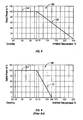
Figure 9. Figure 9 shows aderating curve 68 having ahorizontal portion 70 which commences at -55° C and which extends horizontally to +70° C. The resistor then begins to reduce in efficiency as shown by thenumeral 72, and at +150° C it becomes inoperative. - Therefore, a primary object of the present invention is the provision of a high power resistor having an improved operating temperature range, and a method for making same.
- A further object of the present invention is the provision of a high power resistor which is operable between -65° C and +275° C.
- A further object of the present invention is the provision of a high power resistor which utilizes an adhesive for attaching a heat sink to the resistor element.
- A further object of the present invention is the provision of a high power resistor and method for making same which utilizes an anodized aluminum heat sink.
- A further object of the present invention is the provision of a high power resistor and method for making same which utilizes an improved dielectric molding material surrounding the resistor for improving heat dissipation.
- A further object of the present invention is the provision of a high power resistor and method for making same which provides an improved operating temperature and which occupies a minimum of space.
- A further object of the present invention is the provision of an improved high power resistor and method for making same which is efficient in operation, durable in use, and economical to manufacture.
- The foregoing objects may be achieved by a high power resistor comprising a resistance element having first and second opposite ends. A first lead and a second lead extend from the opposite ends of the resistance element. A heat sink of dielectric material is capable of conducting heat away from the resistance element and is connected to the resistance element in heat conducting relation thereto so as to conduct heat away from the resistance element. The heat conducting relationship of the resistance element and the heat sink render the resistance element capable of operating as a resistor between temperatures of from -65° C to +275° C.
- According to one feature of the present invention the heat sink is comprised of anodized aluminum. This is the preferred material, but other materials such as beryllium oxide or aluminum oxide may be used. Also, copper that has been passivated to create a non-conductive outer surface may also be used.
- According to another feature of the present invention, an adhesive attaches the heat sink to the resistance element. The adhesive has the capability of permitting the resistor to produce resistively throughout heat temperatures in the range of from -65° C to +275° C. The adhesive maintains its adhesion of the resistance element to the heat sink in the range from -65° C to +275° C. The specific adhesive which is Applicant's preferred adhesive is Model No. BA-813J01, manufactured by Tra-Con, Inc. under the name Tra-Bond, but other adhesives may be used.
- According to another feature of the present invention a dielectric molding material surrounds the resistance element, the adhesive and the heat sink. Examples of molding compounds are liquid crystal polymers manufactured by DuPont (having an address of Barley Mill Plaza, Building No. 22, Wilmington, Delaware 19880) under the trademark ZENITE, and under the Model No. 6130L; and a liquid crystal polymer manufactured under the trademark VECTRA, Model No. E130I, by Tucona, a member of the Hoechst Group, 90 Morris Avenue, Summit, New Jersey 07901.
- The method of the present invention comprises forming a resistance element having first and second opposite ends and first and second leads extending from the first and second opposite ends respectively. A heat sink is attached to the resistance element in heat conducting relation thereto so as to render the resistance element capable of producing resistance in the temperature range of -65° C to +275° C.
- The method further comprises forming the resistance element so that the resistance element includes a flat resistance element face. The method includes attaching a flat heat sink surface to the flat resistance element face.
- The method further comprises using an adhesive to attach the heat sink to the resistance element.
- The method further comprises molding a dielectric material completely around the resistance element, the adhesive, and the heat sink.
- The method further comprises forming a pre-molded body on opposite sides of the heat sink before attaching the heat sink to the resistance element.
-
-
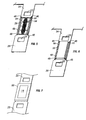
Figure 1 is a perspective view of the high power resistor of the present invention. -
Figure 2 is a perspective view of a strip of material having the various resistor elements formed thereon. -
Figure 3 is a perspective view of a similar resistance element such as shown inFigure 2 , but showing the pre-molded material and the adhesive material applied thereto. -
Figure 4 is a sectional view taken along line 4-4 ofFigure 3 . -
Figure 5 is a perspective view similar toFigure 3 showing the adhesive applied to the resistance element. -
Figure 6 is a view similar toFigures 3 and5 showing the heat sink in place. -
Figure 7 is a perspective view of the resistor after the molding process is complete. -
Figure 8 is a derating curve of the present invention. -
Figure 9 is a derating curve of prior art resistors. - Referring to the drawings the
numeral 10 generally designates a resistor body made according to the present invention.Resistor body 10 includesleads dielectric body 16. Theleads dielectric body 16. An exposedheat sink 18 is shown on the top surface of thebody 10. -
Figure 2 illustrates the first step of development and manufacture of the present invention. Anelongated strip 20 includes a plurality ofresistor blanks 36 extending there from.Strip 20 includes a plurality ofcircular indexing holes 22 which are adapted to receive pins from a conveyor. The pins move thevarious blanks 36 to each of various stations for performing different operations on the blanks 36. - Each blank 36 includes a pair of
square holes 23 which facilitate the bending of theleads leads resistance element 28, and a pair ofweld seams 34 separate theresistance element 28 from the first andsecond leads resistance element 28 is formed of a conventional resistance material. - Extending inwardly from one of the sides of the
resistance element 28 are a plurality ofslots 30 and extending inwardly from the opposite side ofresistance element 28 is aslot 32. The number ofslots arrow 38 which represents the serpentine current path followed as current passes through theresistance element 28.Slots -
Figure 3 shows the next step in the manufacturing process. The blank 36 is pre-molded to form apre-mold body 40.Pre-molded body 40 includes a bottom portion 42 (Figure 4 ),upstanding ridges 44 which extend along the opposite edges of theresistance element 28, and four lands orposts 46 at the four corners of theresistance element 28. Extending inwardly from theupstanding ridges 44 are two spaced apartinner flanges 48 which formslots 50 around the opposite edges ofresistance element 28. A pair of V-shaped bottom grooves 52 extend along the under surface of thebottom portion 42 of the pre-mold 40. -
Figure 5 is the same asFigure 3 , but shows an amount of adhesive 54 which has been applied to the central portion of theresistance element 28. The adhesive should have the properties of maintaining its structural integrity and maintaining its adhesive capabilities in the range of temperatures from -65° C to +275° C. An example of such an adhesive is an epoxy adhesive manufactured by Tra-Con, Inc., 45 Wiggins Avenue, Bedford, Massachusetts 01730 under the trademark TRA-BOND, Model No. BA-813J01. - Referring to
Figure 6 , abody 56 of anodized aluminum is placed over the adhesive 54 so that it is in heat conducting connection to theresistance element 28. Thus heat is conducted from theresistance element 28 through the adhesive 54, and through the anodizedaluminum heat sink 56 to dissipate heat that is generated by theresistance element 28. - After the
heat sink 56 is attached to theresistance element 28 as shown inFigure 6 , theentire resistance element 28,pre-mold 40, adhesive 54, andheat sink 56 are molded in a molding compound to produce the moldedbody 58. The moldedbody 58 includes an exposedportion 18 so that heat may be dissipated directly from theheat sink 56 to the atmosphere. - The molding compound for molding the
body 58 may be selected from a number of molding compounds that are dielectric and capable of conducting heat. Examples of such molding compounds are liquid crystal polymers manufactured by DuPont at Barley Mill Plaza,Building 22, Wilmington, Delaware 19880 under the trademark ZENITE, Model No. 6130L; or manufactured by Tucona, a member of Hoechst Group, 90 Morris Avenue, Summit, New Jersey 07901 under the trademark VECTRA, Model No. E130I. - The leads 24, 26 are bent downwardly and curled under the
body 16 as shown inFigure 1 . -
Figure 8 illustrates the derating curve produced by the resistor of the present invention. The derating curve is designated by the numeral 62 and includes a horizontal portion commencing at -65° and remaining horizontal up to +70° C. Then the derating curve declines downwardly as designated by the numeral 66 until it reaches 0 performance at +275° C. Thus the device of the present invention operates as a resistor between the temperature ranges of -65° C to +275° C. - As can be seen by comparing
Figure 8 to Figure 9 , the performance of the resistor of the present invention commences at 10° below the lowest temperature of the average prior art device and functions as a resistor up to 125° higher than the capabilities of prior art resistors. The resistor of the present invention will function in this temperature range to produce ohmage in the range of from .0075 ohms to .3 ohms, and to dissipate heat up to approximately 5 or 6 watts. - The invention has been shown and described above with the preferred embodiments, and it is understood that many modifications, substitutions, and additions may be made which are within the intended spirit and scope of the invention. From the foregoing, it can be seen that the present invention accomplishes at least all of its stated objectives.
Claims (20)
- A high power resistor comprising:a resistance element;a heat sink comprising a dielectric material; anda heat conductive adhesive between the resistance element and the heat sink, the adhesive conducting heat from the resistance element to the heat sink;wherein the heat conducting relationship of the resistance element, the adhesive, and the heat sink render the resistance element operable as a resistor without power derating between temperatures of -65 degrees Celsius to +275 degrees Celsius.
- The resistor of claim 1, wherein the dielectric material comprises at least one of anodized aluminum, aluminum oxide, beryllium oxide or copper passivated to create a non-conductive outer layer.
- The resistor of claim 1, further comprising first and second leads attached respectively to first and second opposite ends of the resistance element.
- The resistor of claim 1 further comprising a molded body partially surrounding the heat sink, leaving a portion of the heat sink exposed to the atmosphere surrounding the resistor.
- The resistor of claim 4, wherein the molded body completely surrounds the resistance element and the adhesive.
- The resistor of claim 3 wherein the first and second leads are bent downwardly and under a bottom surface of a molded body.
- The resistor of claim 6, wherein the molded body partially surrounds the heat sink, leaving a portion of the heat sink exposed to the atmosphere surrounding the resistor.
- The resistor of claim 3, wherein the first and second leads comprise a material different from material of the resistance element.
- The resistor of claim 1 further comprising a pre-molded body having first and second edges extending between first and second opposite ends of the resistance element retentively engaging the resistance element and including at least two ridges extending along opposite edges of the resistance element that extend between the first and second opposite ends of the resistance element.
- The resistor of claim 1 comprising a plurality of molded bodies interconnected by an elongated strip, each of the molded bodies surrounding the resistance element and the adhesive, and partially surrounding the heat sink.
- A method for making a high power resistor comprising:forming a resistor blank comprising a resistance element;depositing an electrically non-conductive and heat conductive adhesive on a surface of the resistance element, the adhesive having the properties of maintaining structural integrity and adhesive capabilities at temperatures between -65 degrees Celsius and to +275 degrees Celsius; andplacing a dielectric heat sink in contact with the adhesive, the adhesive being situated between the heat sink and a surface of the resistance element, the adhesive establishing a heat conducting relationship between the resistance element and the heat sink such that the resistor is operable without power derating at temperatures between -65°C degrees Celsius and 275 degrees Celsius.
- The method of claim 11, wherein the dielectric heat sink comprises at least one of anodized aluminum, aluminum oxide, beryllium oxide or copper passivated to create a non-conductive outer layer.
- The method of claim 11 further comprising attaching first and second leads respectively to first and second opposite ends of the resistance element.
- The method of claim 13, wherein the attaching comprises welding.
- The method of claim 11, further comprising molding a molded body partially around the heat sink, leaving a portion of the heat sink exposed to the atmosphere surrounding the resistor.
- The method of claim 15 comprising molding the molded body completely around the resistance element and the adhesive.
- The method of claim 13 further comprising:bending the first and second leads into facing relation with a bottom surface of a molded body.
- The method of claim 17, further comprising molding the molded body partially around the heat sink, leaving a portion of the heat sink exposed to the atmosphere surrounding the resistor.
- The method of claim 13 comprising using a material for the first and second leads different from material of the resistance element.
- The method according to claim 11 further comprising forming a pre-molded body having first and second slots that embrace first and second opposite edges of the resistance element, the edges extending between first and second opposite ends of the resistance element.
Applications Claiming Priority (2)
| Application Number | Priority Date | Filing Date | Title |
|---|---|---|---|
| US10/441,649 US7102484B2 (en) | 2003-05-20 | 2003-05-20 | High power resistor having an improved operating temperature range |
| EP04785520A EP1625599B1 (en) | 2003-05-20 | 2004-05-11 | High power resistor having an improved operating temperature range and method for making same |
Related Parent Applications (2)
| Application Number | Title | Priority Date | Filing Date |
|---|---|---|---|
| EP04785520.0 Division | 2004-05-11 | ||
| EP04785520A Division EP1625599B1 (en) | 2003-05-20 | 2004-05-11 | High power resistor having an improved operating temperature range and method for making same |
Publications (2)
| Publication Number | Publication Date |
|---|---|
| EP2228807A1 true EP2228807A1 (en) | 2010-09-15 |
| EP2228807B1 EP2228807B1 (en) | 2016-07-27 |
Family
ID=33450038
Family Applications (2)
| Application Number | Title | Priority Date | Filing Date |
|---|---|---|---|
| EP10167405.9A Expired - Lifetime EP2228807B1 (en) | 2003-05-20 | 2004-05-11 | High power resistor having an improved operating temperature range and method for making same |
| EP04785520A Expired - Lifetime EP1625599B1 (en) | 2003-05-20 | 2004-05-11 | High power resistor having an improved operating temperature range and method for making same |
Family Applications After (1)
| Application Number | Title | Priority Date | Filing Date |
|---|---|---|---|
| EP04785520A Expired - Lifetime EP1625599B1 (en) | 2003-05-20 | 2004-05-11 | High power resistor having an improved operating temperature range and method for making same |
Country Status (7)
| Country | Link |
|---|---|
| US (3) | US7102484B2 (en) |
| EP (2) | EP2228807B1 (en) |
| JP (1) | JP4390806B2 (en) |
| CN (2) | CN100583315C (en) |
| AT (1) | ATE504069T1 (en) |
| DE (1) | DE602004032019D1 (en) |
| WO (1) | WO2004105059A1 (en) |
Cited By (1)
| Publication number | Priority date | Publication date | Assignee | Title |
|---|---|---|---|---|
| EP2602797A3 (en) * | 2011-12-05 | 2013-08-21 | Isabellenhütte Heusler GmbH & Co.KG | Resistor, in particular current-measurement resistor |
Families Citing this family (18)
| Publication number | Priority date | Publication date | Assignee | Title |
|---|---|---|---|---|
| US7190252B2 (en) * | 2005-02-25 | 2007-03-13 | Vishay Dale Electronics, Inc. | Surface mount electrical resistor with thermally conductive, electrically insulative filler and method for using same |
| DE102006033710B4 (en) * | 2006-07-20 | 2013-04-11 | Epcos Ag | Method for producing a resistor arrangement |
| US7948355B2 (en) * | 2007-05-24 | 2011-05-24 | Industrial Technology Research Institute | Embedded resistor devices |
| US7843309B2 (en) * | 2007-09-27 | 2010-11-30 | Vishay Dale Electronics, Inc. | Power resistor |
| WO2009041974A1 (en) * | 2007-09-27 | 2009-04-02 | Vishay Dale Electronics, Inc. | Power resistor |
| CN103093908B (en) * | 2007-09-27 | 2017-04-26 | 韦沙戴尔电子公司 | Power resistor |
| US8248202B2 (en) * | 2009-03-19 | 2012-08-21 | Vishay Dale Electronics, Inc. | Metal strip resistor for mitigating effects of thermal EMF |
| US8325007B2 (en) * | 2009-12-28 | 2012-12-04 | Vishay Dale Electronics, Inc. | Surface mount resistor with terminals for high-power dissipation and method for making same |
| DE102010030317B4 (en) * | 2010-06-21 | 2016-09-01 | Infineon Technologies Ag | Circuit arrangement with shunt resistor |
| CN102097193B (en) * | 2010-12-17 | 2012-07-04 | 江苏浩峰汽车附件有限公司 | Etched resistor production method |
| JP6038439B2 (en) * | 2011-10-14 | 2016-12-07 | ローム株式会社 | Chip resistor, chip resistor mounting structure |
| TWI428940B (en) * | 2011-11-15 | 2014-03-01 | Ta I Technology Co Ltd | Current sensing resistor and method for manufacturing the same |
| US8823483B2 (en) | 2012-12-21 | 2014-09-02 | Vishay Dale Electronics, Inc. | Power resistor with integrated heat spreader |
| US10319501B2 (en) * | 2014-02-27 | 2019-06-11 | Panasonic Intellectual Property Management Co., Ltd. | Chip resistor |
| CN105590712A (en) * | 2014-11-15 | 2016-05-18 | 旺诠股份有限公司 | Manufacturing method of micro-impedance resistor and micro-impedance resistor |
| US10083781B2 (en) | 2015-10-30 | 2018-09-25 | Vishay Dale Electronics, Llc | Surface mount resistors and methods of manufacturing same |
| US10438729B2 (en) | 2017-11-10 | 2019-10-08 | Vishay Dale Electronics, Llc | Resistor with upper surface heat dissipation |
| CN110666040A (en) * | 2019-09-17 | 2020-01-10 | 中国航空制造技术研究院 | Hot stretch bending die and stretch bending forming method of titanium alloy profile |
Citations (2)
| Publication number | Priority date | Publication date | Assignee | Title |
|---|---|---|---|---|
| DE4234022A1 (en) * | 1992-10-09 | 1994-04-14 | Telefunken Microelectron | Layered circuit with power resistor(s) - has extra ceramic carrier layer in heat conductive contact with power resistor |
| US6148502A (en) * | 1997-10-02 | 2000-11-21 | Vishay Sprague, Inc. | Surface mount resistor and a method of making the same |
Family Cites Families (28)
| Publication number | Priority date | Publication date | Assignee | Title |
|---|---|---|---|---|
| US3541489A (en) | 1968-12-26 | 1970-11-17 | Dale Electronics | Resistor |
| US3525065A (en) | 1969-02-03 | 1970-08-18 | Dale Electronics | Heat dissipating resistor |
| US3649944A (en) * | 1970-05-25 | 1972-03-14 | Richard E Caddock | Film-type power resistor |
| US3955169A (en) | 1974-11-08 | 1976-05-04 | The United States Of America As Represented By The Secretary Of The Air Force | High power resistor |
| US4064477A (en) * | 1975-08-25 | 1977-12-20 | American Components Inc. | Metal foil resistor |
| US4196411A (en) * | 1978-06-26 | 1980-04-01 | Gentron Corporation | Dual resistor element |
| US4455744A (en) * | 1979-09-04 | 1984-06-26 | Vishay Intertechnology, Inc. | Method of making a precision resistor with improved temperature characteristics |
| US4529958A (en) * | 1983-05-02 | 1985-07-16 | Dale Electronics, Inc. | Electrical resistor |
| US4719443A (en) | 1986-04-03 | 1988-01-12 | General Electric Company | Low capacitance power resistor using beryllia dielectric heat sink layer and low toxicity method for its manufacture |
| US4829553A (en) * | 1988-01-19 | 1989-05-09 | Matsushita Electric Industrial Co., Ltd. | Chip type component |
| US5179366A (en) * | 1991-06-24 | 1993-01-12 | Motorola, Inc. | End terminated high power chip resistor assembly |
| US5304977A (en) * | 1991-09-12 | 1994-04-19 | Caddock Electronics, Inc. | Film-type power resistor combination with anchored exposed substrate/heatsink |
| US5287083A (en) * | 1992-03-30 | 1994-02-15 | Dale Electronics, Inc. | Bulk metal chip resistor |
| JP2899180B2 (en) | 1992-09-01 | 1999-06-02 | キヤノン株式会社 | Image heating device and image heating heater |
| US5291175A (en) * | 1992-09-28 | 1994-03-01 | Ohmite Manufacturing Co. | Limiting heat flow in planar, high-density power resistors |
| US5355281A (en) * | 1993-06-29 | 1994-10-11 | E.B.G. Elektronische Bauelemente Gesellschaft M.B.H. | Electrical device having a bonded ceramic-copper heat transfer medium |
| US5481241A (en) * | 1993-11-12 | 1996-01-02 | Caddock Electronics, Inc. | Film-type heat sink-mounted power resistor combination having only a thin encapsulant, and having an enlarged internal heat sink |
| US5621378A (en) * | 1995-04-20 | 1997-04-15 | Caddock Electronics, Inc. | Heatsink-mountable power resistor having improved heat-transfer interface with the heatsink |
| US5739743A (en) * | 1996-02-05 | 1998-04-14 | Emc Technology, Inc. | Asymmetric resistor terminal |
| US5999085A (en) | 1998-02-13 | 1999-12-07 | Vishay Dale Electronics, Inc. | Surface mounted four terminal resistor |
| TW393744B (en) * | 1998-11-10 | 2000-06-11 | Siliconware Precision Industries Co Ltd | A semicondutor packaging |
| US5945905A (en) * | 1998-12-21 | 1999-08-31 | Emc Technology Llc | High power resistor |
| US6404324B1 (en) * | 1999-09-07 | 2002-06-11 | General Motors Corporation | Resistive component for use with short duration, high-magnitude currents |
| US6510605B1 (en) | 1999-12-21 | 2003-01-28 | Vishay Dale Electronics, Inc. | Method for making formed surface mount resistor |
| JP3803025B2 (en) * | 2000-12-05 | 2006-08-02 | 富士電機ホールディングス株式会社 | Resistor |
| US6600651B1 (en) * | 2001-06-05 | 2003-07-29 | Macronix International Co., Ltd. | Package with high heat dissipation |
| US6340927B1 (en) * | 2001-06-29 | 2002-01-22 | Elektronische Bauelemente Gesellschaft M.B.H | High thermal efficiency power resistor |
| US6660651B1 (en) | 2001-11-08 | 2003-12-09 | Advanced Micro Devices, Inc. | Adjustable wafer stage, and a method and system for performing process operations using same |
-
2003
- 2003-05-20 US US10/441,649 patent/US7102484B2/en not_active Expired - Lifetime
- 2003-12-23 US US10/744,846 patent/US6925704B1/en not_active Expired - Lifetime
-
2004
- 2004-05-11 DE DE602004032019T patent/DE602004032019D1/en not_active Expired - Lifetime
- 2004-05-11 CN CN200480020518A patent/CN100583315C/en not_active Expired - Lifetime
- 2004-05-11 AT AT04785520T patent/ATE504069T1/en not_active IP Right Cessation
- 2004-05-11 WO PCT/US2004/014569 patent/WO2004105059A1/en not_active Ceased
- 2004-05-11 EP EP10167405.9A patent/EP2228807B1/en not_active Expired - Lifetime
- 2004-05-11 JP JP2006532918A patent/JP4390806B2/en not_active Expired - Lifetime
- 2004-05-11 CN CN2009102538592A patent/CN101702355B/en not_active Expired - Lifetime
- 2004-05-11 EP EP04785520A patent/EP1625599B1/en not_active Expired - Lifetime
-
2005
- 2005-05-05 US US11/123,508 patent/US7042328B2/en not_active Expired - Lifetime
Patent Citations (2)
| Publication number | Priority date | Publication date | Assignee | Title |
|---|---|---|---|---|
| DE4234022A1 (en) * | 1992-10-09 | 1994-04-14 | Telefunken Microelectron | Layered circuit with power resistor(s) - has extra ceramic carrier layer in heat conductive contact with power resistor |
| US6148502A (en) * | 1997-10-02 | 2000-11-21 | Vishay Sprague, Inc. | Surface mount resistor and a method of making the same |
Cited By (1)
| Publication number | Priority date | Publication date | Assignee | Title |
|---|---|---|---|---|
| EP2602797A3 (en) * | 2011-12-05 | 2013-08-21 | Isabellenhütte Heusler GmbH & Co.KG | Resistor, in particular current-measurement resistor |
Also Published As
| Publication number | Publication date |
|---|---|
| US7102484B2 (en) | 2006-09-05 |
| HK1142990A1 (en) | 2010-12-17 |
| EP1625599B1 (en) | 2011-03-30 |
| US20050212649A1 (en) | 2005-09-29 |
| WO2004105059A1 (en) | 2004-12-02 |
| DE602004032019D1 (en) | 2011-05-12 |
| JP2006529059A (en) | 2006-12-28 |
| JP4390806B2 (en) | 2009-12-24 |
| ATE504069T1 (en) | 2011-04-15 |
| US20040233032A1 (en) | 2004-11-25 |
| CN1823395A (en) | 2006-08-23 |
| US7042328B2 (en) | 2006-05-09 |
| EP2228807B1 (en) | 2016-07-27 |
| CN101702355B (en) | 2012-05-23 |
| EP1625599A1 (en) | 2006-02-15 |
| CN101702355A (en) | 2010-05-05 |
| CN100583315C (en) | 2010-01-20 |
| US6925704B1 (en) | 2005-08-09 |
Similar Documents
| Publication | Publication Date | Title |
|---|---|---|
| EP2228807B1 (en) | High power resistor having an improved operating temperature range and method for making same | |
| EP1851776B1 (en) | Surface mount electrical resistor with thermally conductive, electrically non-conductive filler and method for producing the same | |
| US7843309B2 (en) | Power resistor | |
| JP3260750B2 (en) | Self-regulating PTC device with molded layered conductive terminals | |
| KR101753271B1 (en) | Flexible heating element and manufacturing method thereof | |
| WO2009005108A1 (en) | Resistor | |
| JPH0317166B2 (en) | ||
| JPS6230306A (en) | Connection strip for manufacture of directly carried electronic component and manufacture of same electronic component | |
| JP4640952B2 (en) | Chip resistor and manufacturing method thereof | |
| EP2215639A1 (en) | Power resistor | |
| US11648766B1 (en) | Process for making a flexible foil heater | |
| TW201407646A (en) | Mass production method of metal plate resistor and product thereof | |
| JP2898336B2 (en) | Manufacturing method of PTC thermistor | |
| HK1142990B (en) | High power resistor having an improved operating temperature range and method for making same | |
| TWI260846B (en) | Over-current protection device | |
| JP2001052901A (en) | Chip organic positive temperature coefficient thermistor and manufacturing method therefor | |
| HK1112106B (en) | Surface mount electrical resistor with thermally conductive, electrically non-conductive filler and method for producing the same | |
| HK1112106A (en) | Surface mount electrical resistor with thermally conductive, electrically non-conductive filler and method for producing the same | |
| TWI261847B (en) | Manufacturing process of high-precision alloy resistor | |
| JP2005303050A (en) | Spacer tape for film carrier tape for mounting electronic components | |
| JPS60208802A (en) | Nonlinear resistance element and method of producing same | |
| KR20130006075U (en) | Circuit protection device |
Legal Events
| Date | Code | Title | Description |
|---|---|---|---|
| PUAI | Public reference made under article 153(3) epc to a published international application that has entered the european phase |
Free format text: ORIGINAL CODE: 0009012 |
|
| 17P | Request for examination filed |
Effective date: 20100625 |
|
| AC | Divisional application: reference to earlier application |
Ref document number: 1625599 Country of ref document: EP Kind code of ref document: P |
|
| AK | Designated contracting states |
Kind code of ref document: A1 Designated state(s): AT BE BG CH CY CZ DE DK EE ES FI FR GB GR HU IE IT LI LU MC NL PL PT RO SE SI SK TR |
|
| 17Q | First examination report despatched |
Effective date: 20150811 |
|
| GRAP | Despatch of communication of intention to grant a patent |
Free format text: ORIGINAL CODE: EPIDOSNIGR1 |
|
| RIN1 | Information on inventor provided before grant (corrected) |
Inventor name: WELK, NATHAN Inventor name: HENDRICKS, STEVE Inventor name: SMEJKAL, JOEL J. Inventor name: TRAUDT, BRANDON Inventor name: MIKSCH, RONALD Inventor name: LANGE, DAVID L. Inventor name: SCHNEEKLOTH, GREG |
|
| INTG | Intention to grant announced |
Effective date: 20160229 |
|
| GRAS | Grant fee paid |
Free format text: ORIGINAL CODE: EPIDOSNIGR3 |
|
| GRAA | (expected) grant |
Free format text: ORIGINAL CODE: 0009210 |
|
| AC | Divisional application: reference to earlier application |
Ref document number: 1625599 Country of ref document: EP Kind code of ref document: P |
|
| AK | Designated contracting states |
Kind code of ref document: B1 Designated state(s): AT BE BG CH CY CZ DE DK EE ES FI FR GB GR HU IE IT LI LU MC NL PL PT RO SE SI SK TR |
|
| REG | Reference to a national code |
Ref country code: GB Ref legal event code: FG4D |
|
| REG | Reference to a national code |
Ref country code: CH Ref legal event code: EP |
|
| REG | Reference to a national code |
Ref country code: AT Ref legal event code: REF Ref document number: 816378 Country of ref document: AT Kind code of ref document: T Effective date: 20160815 |
|
| REG | Reference to a national code |
Ref country code: IE Ref legal event code: FG4D |
|
| REG | Reference to a national code |
Ref country code: DE Ref legal event code: R096 Ref document number: 602004049685 Country of ref document: DE |
|
| REG | Reference to a national code |
Ref country code: NL Ref legal event code: MP Effective date: 20160727 |
|
| REG | Reference to a national code |
Ref country code: AT Ref legal event code: MK05 Ref document number: 816378 Country of ref document: AT Kind code of ref document: T Effective date: 20160727 |
|
| PG25 | Lapsed in a contracting state [announced via postgrant information from national office to epo] |
Ref country code: FI Free format text: LAPSE BECAUSE OF FAILURE TO SUBMIT A TRANSLATION OF THE DESCRIPTION OR TO PAY THE FEE WITHIN THE PRESCRIBED TIME-LIMIT Effective date: 20160727 Ref country code: IT Free format text: LAPSE BECAUSE OF FAILURE TO SUBMIT A TRANSLATION OF THE DESCRIPTION OR TO PAY THE FEE WITHIN THE PRESCRIBED TIME-LIMIT Effective date: 20160727 Ref country code: NL Free format text: LAPSE BECAUSE OF FAILURE TO SUBMIT A TRANSLATION OF THE DESCRIPTION OR TO PAY THE FEE WITHIN THE PRESCRIBED TIME-LIMIT Effective date: 20160727 |
|
| PG25 | Lapsed in a contracting state [announced via postgrant information from national office to epo] |
Ref country code: SE Free format text: LAPSE BECAUSE OF FAILURE TO SUBMIT A TRANSLATION OF THE DESCRIPTION OR TO PAY THE FEE WITHIN THE PRESCRIBED TIME-LIMIT Effective date: 20160727 Ref country code: GR Free format text: LAPSE BECAUSE OF FAILURE TO SUBMIT A TRANSLATION OF THE DESCRIPTION OR TO PAY THE FEE WITHIN THE PRESCRIBED TIME-LIMIT Effective date: 20161028 Ref country code: BE Free format text: LAPSE BECAUSE OF FAILURE TO SUBMIT A TRANSLATION OF THE DESCRIPTION OR TO PAY THE FEE WITHIN THE PRESCRIBED TIME-LIMIT Effective date: 20160727 Ref country code: AT Free format text: LAPSE BECAUSE OF FAILURE TO SUBMIT A TRANSLATION OF THE DESCRIPTION OR TO PAY THE FEE WITHIN THE PRESCRIBED TIME-LIMIT Effective date: 20160727 Ref country code: ES Free format text: LAPSE BECAUSE OF FAILURE TO SUBMIT A TRANSLATION OF THE DESCRIPTION OR TO PAY THE FEE WITHIN THE PRESCRIBED TIME-LIMIT Effective date: 20160727 Ref country code: PL Free format text: LAPSE BECAUSE OF FAILURE TO SUBMIT A TRANSLATION OF THE DESCRIPTION OR TO PAY THE FEE WITHIN THE PRESCRIBED TIME-LIMIT Effective date: 20160727 Ref country code: PT Free format text: LAPSE BECAUSE OF FAILURE TO SUBMIT A TRANSLATION OF THE DESCRIPTION OR TO PAY THE FEE WITHIN THE PRESCRIBED TIME-LIMIT Effective date: 20161128 |
|
| REG | Reference to a national code |
Ref country code: FR Ref legal event code: PLFP Year of fee payment: 14 |
|
| PG25 | Lapsed in a contracting state [announced via postgrant information from national office to epo] |
Ref country code: EE Free format text: LAPSE BECAUSE OF FAILURE TO SUBMIT A TRANSLATION OF THE DESCRIPTION OR TO PAY THE FEE WITHIN THE PRESCRIBED TIME-LIMIT Effective date: 20160727 Ref country code: RO Free format text: LAPSE BECAUSE OF FAILURE TO SUBMIT A TRANSLATION OF THE DESCRIPTION OR TO PAY THE FEE WITHIN THE PRESCRIBED TIME-LIMIT Effective date: 20160727 |
|
| REG | Reference to a national code |
Ref country code: DE Ref legal event code: R097 Ref document number: 602004049685 Country of ref document: DE |
|
| PG25 | Lapsed in a contracting state [announced via postgrant information from national office to epo] |
Ref country code: CZ Free format text: LAPSE BECAUSE OF FAILURE TO SUBMIT A TRANSLATION OF THE DESCRIPTION OR TO PAY THE FEE WITHIN THE PRESCRIBED TIME-LIMIT Effective date: 20160727 Ref country code: SK Free format text: LAPSE BECAUSE OF FAILURE TO SUBMIT A TRANSLATION OF THE DESCRIPTION OR TO PAY THE FEE WITHIN THE PRESCRIBED TIME-LIMIT Effective date: 20160727 Ref country code: DK Free format text: LAPSE BECAUSE OF FAILURE TO SUBMIT A TRANSLATION OF THE DESCRIPTION OR TO PAY THE FEE WITHIN THE PRESCRIBED TIME-LIMIT Effective date: 20160727 Ref country code: BG Free format text: LAPSE BECAUSE OF FAILURE TO SUBMIT A TRANSLATION OF THE DESCRIPTION OR TO PAY THE FEE WITHIN THE PRESCRIBED TIME-LIMIT Effective date: 20161027 |
|
| PLBE | No opposition filed within time limit |
Free format text: ORIGINAL CODE: 0009261 |
|
| STAA | Information on the status of an ep patent application or granted ep patent |
Free format text: STATUS: NO OPPOSITION FILED WITHIN TIME LIMIT |
|
| 26N | No opposition filed |
Effective date: 20170502 |
|
| PG25 | Lapsed in a contracting state [announced via postgrant information from national office to epo] |
Ref country code: LU Free format text: LAPSE BECAUSE OF NON-PAYMENT OF DUE FEES Effective date: 20170531 Ref country code: SI Free format text: LAPSE BECAUSE OF FAILURE TO SUBMIT A TRANSLATION OF THE DESCRIPTION OR TO PAY THE FEE WITHIN THE PRESCRIBED TIME-LIMIT Effective date: 20160727 |
|
| REG | Reference to a national code |
Ref country code: CH Ref legal event code: PL |
|
| PG25 | Lapsed in a contracting state [announced via postgrant information from national office to epo] |
Ref country code: MC Free format text: LAPSE BECAUSE OF FAILURE TO SUBMIT A TRANSLATION OF THE DESCRIPTION OR TO PAY THE FEE WITHIN THE PRESCRIBED TIME-LIMIT Effective date: 20160727 |
|
| REG | Reference to a national code |
Ref country code: IE Ref legal event code: MM4A |
|
| PG25 | Lapsed in a contracting state [announced via postgrant information from national office to epo] |
Ref country code: CH Free format text: LAPSE BECAUSE OF NON-PAYMENT OF DUE FEES Effective date: 20170531 Ref country code: LI Free format text: LAPSE BECAUSE OF NON-PAYMENT OF DUE FEES Effective date: 20170531 |
|
| PG25 | Lapsed in a contracting state [announced via postgrant information from national office to epo] |
Ref country code: LU Free format text: LAPSE BECAUSE OF NON-PAYMENT OF DUE FEES Effective date: 20170511 |
|
| PG25 | Lapsed in a contracting state [announced via postgrant information from national office to epo] |
Ref country code: IE Free format text: LAPSE BECAUSE OF NON-PAYMENT OF DUE FEES Effective date: 20170511 |
|
| REG | Reference to a national code |
Ref country code: FR Ref legal event code: PLFP Year of fee payment: 15 |
|
| PG25 | Lapsed in a contracting state [announced via postgrant information from national office to epo] |
Ref country code: HU Free format text: LAPSE BECAUSE OF FAILURE TO SUBMIT A TRANSLATION OF THE DESCRIPTION OR TO PAY THE FEE WITHIN THE PRESCRIBED TIME-LIMIT; INVALID AB INITIO Effective date: 20040511 |
|
| PG25 | Lapsed in a contracting state [announced via postgrant information from national office to epo] |
Ref country code: CY Free format text: LAPSE BECAUSE OF NON-PAYMENT OF DUE FEES Effective date: 20160727 |
|
| PG25 | Lapsed in a contracting state [announced via postgrant information from national office to epo] |
Ref country code: TR Free format text: LAPSE BECAUSE OF FAILURE TO SUBMIT A TRANSLATION OF THE DESCRIPTION OR TO PAY THE FEE WITHIN THE PRESCRIBED TIME-LIMIT Effective date: 20160727 |
|
| PGFP | Annual fee paid to national office [announced via postgrant information from national office to epo] |
Ref country code: FR Payment date: 20230510 Year of fee payment: 20 Ref country code: DE Payment date: 20230425 Year of fee payment: 20 |
|
| PGFP | Annual fee paid to national office [announced via postgrant information from national office to epo] |
Ref country code: GB Payment date: 20230427 Year of fee payment: 20 |
|
| REG | Reference to a national code |
Ref country code: DE Ref legal event code: R071 Ref document number: 602004049685 Country of ref document: DE |
|
| REG | Reference to a national code |
Ref country code: GB Ref legal event code: PE20 Expiry date: 20240510 |
|
| PG25 | Lapsed in a contracting state [announced via postgrant information from national office to epo] |
Ref country code: GB Free format text: LAPSE BECAUSE OF EXPIRATION OF PROTECTION Effective date: 20240510 |
|
| PG25 | Lapsed in a contracting state [announced via postgrant information from national office to epo] |
Ref country code: GB Free format text: LAPSE BECAUSE OF EXPIRATION OF PROTECTION Effective date: 20240510 |