EP2225752B1 - Video rendering across a high speed peripheral interconnect bus - Google Patents
Video rendering across a high speed peripheral interconnect bus Download PDFInfo
- Publication number
- EP2225752B1 EP2225752B1 EP08856301.0A EP08856301A EP2225752B1 EP 2225752 B1 EP2225752 B1 EP 2225752B1 EP 08856301 A EP08856301 A EP 08856301A EP 2225752 B1 EP2225752 B1 EP 2225752B1
- Authority
- EP
- European Patent Office
- Prior art keywords
- graphics
- computing device
- memory
- display
- graphics subsystem
- Prior art date
- Legal status (The legal status is an assumption and is not a legal conclusion. Google has not performed a legal analysis and makes no representation as to the accuracy of the status listed.)
- Active
Links
- 230000002093 peripheral effect Effects 0.000 title claims description 24
- 238000009877 rendering Methods 0.000 title claims description 22
- 239000000872 buffer Substances 0.000 claims description 127
- 238000004891 communication Methods 0.000 claims description 10
- 238000000034 method Methods 0.000 claims description 10
- 238000003032 molecular docking Methods 0.000 claims description 5
- 238000012546 transfer Methods 0.000 description 16
- 238000010586 diagram Methods 0.000 description 10
- 230000007704 transition Effects 0.000 description 6
- 230000000694 effects Effects 0.000 description 4
- 230000008672 reprogramming Effects 0.000 description 3
- 230000006870 function Effects 0.000 description 2
- 230000010354 integration Effects 0.000 description 2
- 230000004048 modification Effects 0.000 description 2
- 238000012986 modification Methods 0.000 description 2
- 230000008569 process Effects 0.000 description 2
- 238000012545 processing Methods 0.000 description 2
- 230000009286 beneficial effect Effects 0.000 description 1
- 230000008901 benefit Effects 0.000 description 1
- 230000008859 change Effects 0.000 description 1
- 230000000295 complement effect Effects 0.000 description 1
- 239000002131 composite material Substances 0.000 description 1
- 239000000446 fuel Substances 0.000 description 1
- 230000006855 networking Effects 0.000 description 1
- 230000003287 optical effect Effects 0.000 description 1
- 230000008520 organization Effects 0.000 description 1
- 230000009467 reduction Effects 0.000 description 1
- 238000005070 sampling Methods 0.000 description 1
Images


Classifications
-
- G—PHYSICS
- G09—EDUCATION; CRYPTOGRAPHY; DISPLAY; ADVERTISING; SEALS
- G09G—ARRANGEMENTS OR CIRCUITS FOR CONTROL OF INDICATING DEVICES USING STATIC MEANS TO PRESENT VARIABLE INFORMATION
- G09G5/00—Control arrangements or circuits for visual indicators common to cathode-ray tube indicators and other visual indicators
- G09G5/36—Control arrangements or circuits for visual indicators common to cathode-ray tube indicators and other visual indicators characterised by the display of a graphic pattern, e.g. using an all-points-addressable [APA] memory
- G09G5/363—Graphics controllers
-
- G—PHYSICS
- G06—COMPUTING; CALCULATING OR COUNTING
- G06F—ELECTRIC DIGITAL DATA PROCESSING
- G06F3/00—Input arrangements for transferring data to be processed into a form capable of being handled by the computer; Output arrangements for transferring data from processing unit to output unit, e.g. interface arrangements
- G06F3/14—Digital output to display device ; Cooperation and interconnection of the display device with other functional units
-
- G—PHYSICS
- G06—COMPUTING; CALCULATING OR COUNTING
- G06T—IMAGE DATA PROCESSING OR GENERATION, IN GENERAL
- G06T1/00—General purpose image data processing
- G06T1/20—Processor architectures; Processor configuration, e.g. pipelining
-
- G—PHYSICS
- G09—EDUCATION; CRYPTOGRAPHY; DISPLAY; ADVERTISING; SEALS
- G09G—ARRANGEMENTS OR CIRCUITS FOR CONTROL OF INDICATING DEVICES USING STATIC MEANS TO PRESENT VARIABLE INFORMATION
- G09G5/00—Control arrangements or circuits for visual indicators common to cathode-ray tube indicators and other visual indicators
- G09G5/36—Control arrangements or circuits for visual indicators common to cathode-ray tube indicators and other visual indicators characterised by the display of a graphic pattern, e.g. using an all-points-addressable [APA] memory
- G09G5/39—Control of the bit-mapped memory
- G09G5/395—Arrangements specially adapted for transferring the contents of the bit-mapped memory to the screen
- G09G5/397—Arrangements specially adapted for transferring the contents of two or more bit-mapped memories to the screen simultaneously, e.g. for mixing or overlay
Definitions
- the present invention relates generally to computing devices, and more particularly to a computing device including graphics processors interconnected by a high speed peripheral bus.
- Computer peripherals are often formed as part of an integrated chipset that cooperates with a central processor.
- Computer audio, graphics adapters and interfaces form part of the integrated chipsets. Such integration reduces costs and size of the computing devices.
- graphics processors are steadily evolving to provide enhanced performance and features.
- Leading graphics processors are nearly as complex as central processors.
- high performance graphics processors are still typically formed on peripheral cards.
- Integrated graphics processors are by comparison, relatively simple and do not provide the features or performance of the high performance, graphics processors formed on peripheral cards.
- integrated graphics components In the presence of an add-on peripheral card, integrated graphics components when present, are typically redundant and therefore disabled.
- graphics adapters whether integrated or external, are upgraded there is often no role for less powerful adapters, and these are disposed of or disabled.
- United States patent application publication no. 2006/0267987 discloses a master/slave graphics adapter arrangement according to which a computing device includes first and second graphics adapters.
- a graphics processor of the first graphics adapter acts as a master graphics processor, while the second graphics adapter acts as a slave.
- the master graphics processor renders graphics to be displayed on multiple separate displays within frame buffer memory of the first graphics adapter. Images to be displayed on one of the separate displays are transferred from frame buffer memory of the first graphics adapter to frame buffer memory of the second graphics adapter.
- Other documents in this technical field are US 2005/285863 and US 5 896 141 .
- graphics generated by one graphics processor are transferred across a high speed expansion/interconnect bus to a frame buffer.
- the rendered frames from the frame buffer are presented on a display by way of a display interface in communication with the frame buffer.
- the display interface of another existing (e.g. integrated) graphics adapter/subsystem may be used to present the rendered frames on an interconnected display.
- the graphics processor may form part of a graphics adapter that need not include a display interface or possibly even a frame buffer. Likewise, the graphics processor may be replaced with a more current graphics processor.
- the graphics processor may form part of a graphics adapter contained on a peripheral expansion card.
- a graphics subsystem for connection to a host computing device according to claim 6.
- a third aspect of the present invention provides a computing device comprising the graphics subsystem and the host device according to claim 8.
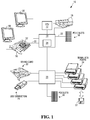
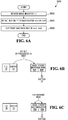
- FIG. 1 is a simplified schematic block diagram of a computing device exemplary of an embodiment of the present invention.
- Computing device 10 is based on a conventional Intel x 86 architecture. However, as will become apparent, the invention may easily be embodied in computing devices having a PowerPC, AMD x 86 or other architecture.
- Computing device 10 includes a processor 12 , interconnected to system memory 16 and peripherals through integrated interface circuits 14 and 20 .
- Processor 12 in exemplary computing device 10 is a conventional central processing unit and may for example be a microprocessor compatible with the INTEL.TM. x 86 family of microprocessors.
- Integrated interface circuits 14 and 20 are often referred to as a north bridge and south bridge, respectively, and provide an interface for processor 12 to peripherals and memory.
- north bridge 14 interconnects the processor 12 ; memory 16 ; a plurality of expansion slots 18 by way of a high speed interconnect bus 22 ; and south bridge 20 .
- South bridge 20 in turn, interconnects lower speed peripherals and interconnects, such as disk drives by way of integrated IDE/SATA ports 24 , universal serial bus devices by way of integrated universal serial bus (USB) ports 26 ; and other peripherals by way of a lower speed interconnect bus 28 , compliant for example, with known PCI or ISA standards.
- South bridge 20 may further include integrated audio components 30 , networking interfaces (not shown) and the like.
- An exemplary interconnect bus 22 is the PCI express (PCIe) bus, that has a bandwidth in the gigabyte per second range, and allows data transfer reads and writes at this bandwidth.
- PCIe PCI express
- current PCle bus speeds allow bi-directional data transfer at speeds of up to 266 MHz or 533 MHz, allowing data rates of up to 2.1 G bytes per second or 4.2 G bytes per second.
- north bridge 14 further includes an integrated graphics adapter 34 suitable for interconnecting computing device 10 to a first display 32 in the form of a monitor, LCD panel, television or the like.
- an additional graphics adapter 52 interconnected by way of interconnect bus 22 forming for example, part of peripheral expansion card 50 within expansion slots 18 on interconnect bus 22 may further be part of computing device 10 .
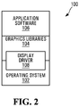
- computing device 10 executes software stored within memory 16 .
- exemplary software 100 includes an operation system 102 , graphics libraries 104 and application software 106 , stored within memory 16 .
- Exemplary operating systems include Windows Vista, Windows XP; Windows NT 4.0 , Windows ME; Windows 98 , Windows 2000 , Windows 95 , or Linux operating systems.
- Exemplary graphics libraries include the Microsoft DirectX libraries and the OpenGL libraries.
- Computer memory 16 ( FIG. 1 ) and interconnected disk drives include a suitable combination of random access memory, read-only memory and disk storage memory, used by device 10 to store and execute operating system and graphics adapter driver programs adapting device 10 in manners exemplary of the embodiments of the present invention.
- Exemplary software 100 FIG.
- Computer readable medium 27 may be an optical storage medium, a magnetic diskette, tape, ROM cartridge or the like.
- Graphics libraries 104 or operating system 102 further include a graphics driver software 108 , used for low-level communication with graphics adapters 34 and 52 .
- the software is layered, with higher level layers using lower layers to provide certain functionality.
- Applications may make use of the operating system 102 and graphics libraries 104 to render 2 D or 3 D graphics.
- Render in this context, includes drawing, or otherwise creating a graphic image for presentation, and may for example include polygon rendering, ray-tracing, image decoding, line drawing or the like.
- software exemplary of embodiments of the present invention may form part of graphics libraries 104 and/or driver software 108 .
- exemplary software may form part of the OpenGL library and associated drivers.
- OpenGL is more particularly detailed in The Official Guide to Learning OpenGL, Version 1.1 , the contents of which are hereby incorporated by reference.
- a person of ordinary skill will, however, appreciate that methods exemplary of embodiments of the present invention may form part of Microsoft Direct 3 D libraries, applications (such as games) that do not use custom libraries or routine, or any other 3 D application or library.
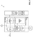
- north bridge 14 includes a high speed bus interface 36 , and memory controller 38 , interconnecting bridge 14 to interconnect bus 22 and system memory 16 .
- North bridge 14 further includes integrated graphics adapter 34 , that in turn includes a graphics processor 40 , a command processor 42 and a display interface 44 .
- Graphics processor 40 may take the form of a three dimensional (3D) graphics processor capable of rendering three dimensional images within a frame buffer 46 allocated within system memory 16 , and may include multiple pipelines and pipeline stages for accelerated rendering of graphics.
- 3D three dimensional
- command processor 42 may include registers used to define a command queue 47 in memory 16 .
- Application software 106 or operating system 102 uses libraries 104 to render graphics images.
- Driver software 108 generates graphics processor specific commands, and places these in the command queue 47 , while also updating registers of command processor 42 to reflect the end of the queue.
- Graphics processor 42 processes queued commands asynchronously, in a pipelined manner in order to, among other things, render images within frame buffer 46 .
- graphics processor 40 is able to process the next command in the queue, it provides a signal to command processor 42 , which in turn fetches the next command in the queue 47 and advances the queue pointer in registers of command processor 42 .
- Display interface 44 by way of memory controller 38 samples the frame buffer 46 and presents an image on one or more video output ports 48 in the form of VGA ports; composite video ports; DVI ports; HDMI; DisplayPort, or the like, for display of one or more video images on video devices such as display 32 ( FIG. 1 ), in the form of a television, monitor or the like. In this way, images rendered by graphics processor 40 in frame buffer 46 may be presented.
- display interface 44 may be any suitable interface for converting data within buffer for display on a display device.
- display interface 44 may take the form of a RAMDAC.
- Display interface 44 is typically programmable, for example through a plurality of registers, allowing driver software 108 or similar software or graphics processor 40 to set the beginning address within memory 16 to present at its display output.
- interface 44 pixel depth (i.e. bits per pixel) and screen resolution are typically programmable.
- two frame buffers may be allocated.
- the buffers may be used alternatively to more smoothly present rendered graphics.
- Display interface 44 only displays contents of one of the two buffers at any time.
- the buffer being displayed is typically referred to as the front buffer.
- Graphics processor 40 renders images for display to the so-called back buffer the frame buffer that is currently not being displayed by display interface 44 .
- front and back buffers are flipped: display interface 44 is programmed to present the former back buffer. In this way, transition between sequential frames rendered by graphics processor 40 may appear smooth.
- registers and frame buffer memory 46 used by adapter 34 are all mapped to addresses within global memory space.
- computing device 10 further includes a graphics adapter 52 formed on a peripheral expansion card 50 that may be inserted into device 10 by way of an expansion slot on high speed interconnect bus 22 , in communication with north bridge 14 , as illustrated in FIG. 1 .
- Graphics adapter 52 as interconnected to north bridge 14 , is schematically illustrated in FIG. 4 .
- graphics adapter 52 includes a graphics processor 54 , video memory 56 , a command processor 58 a memory controller 60 , and a display interface 62 .
- One or more ports 64 , 66 allow interconnection of adapter 52 to one or more display devices, like display 68 ( FIG. 1 ).
- Command processor 58 and display interface 62 function in much the same way as command processor 42 and display interface 44 , respectively.
- Graphics processor 54 operates in much the same way as graphics processor 40 , in its normal mode of operation.
- Graphics adapter 52 includes its own memory 56 , and a memory controller 60 to provide access to memory 56 and system memory 16 .
- Local memory 56 is used to hold, among other things, one or more buffer(s) 70 for graphics adapter 52 used by graphics processor 54 , that may act as frame buffer(s).
- a command queue 57 for graphics processor 54 is also established in system memory 16 .
- local memory 56 is addressable at addresses within global system memory space, through memory controller 60 .
- registers used by command processor 54 and display interface 62 are addressable at addresses within global address space.
- registers and frame buffer 46 used by adapter 34 are mapped to global memory space.
- command processor 58 and graphics processor 54 may write to frame buffer 46 and registers used by display interface 44 and command processor 42 .
- graphics processor 54 in conjunction with memory controller 60 is operable to perform block transfer operations to transfer data from and to system and adapter memory 16 , 56 at memory addresses.
- integrated graphics adapter 34 provides limited functionality. For example, resolution, 3 D graphics abilities, and the like of integrated graphics controller are relatively limited. Thus, integrated graphics adapter 34 typically has significantly less graphics processing ability than graphics adapter 52 . For example, adapter 34 may operate more slowly than adapter 52 , provide less features, and the like.
- integrated adapter 34 or adapter 52 may, or may not, by itself allow the interconnection of multiple physical display devices, by way of multiple ports like port 48 .
- Each adapter may be interconnected with at least one physical display.
- adapter driver software 108 loaded within memory 16 causes graphics adapter 52 to act as a master (or first) graphics adapter rendering graphics for presentation at both displays 32 and 68 , and graphics adapter 34 , as a second or slave adapter.
- integrated graphics adapter 34 is substantially disabled. However, components of on-board graphics adapter 34 (and in particular display interface 44 ) may still be used to drive interconnected monitors and other display devices. As such, card 50 need not include multiple display ports and display drivers. Instead, display interface 44 and its port(s) 48 may be used to drive at least one monitor or display 32 , in addition to the display 68 or displays driven by card 50 . If adapter 52 includes multiple ports (such as ports 64 , 66 ), processor 52 may additionally render images for presentation through these multiple ports. Of course, driver software 108 may also allow operation of adapter 34 in its conventional mode of operation, described above. Selection of the mode of operation of adapter 34 (and hence adapter 52 ) may be made by or through application software 106.
- driver software 108 within memory 16 allocates an active frame buffer 70 and a secondary adapter buffer 72 within memory 56 of adapter 52 , as schematically depicted in FIG. 4 .
- the active frame buffer 70 functions as a conventional frame buffer for adapter 52 , and thus stores frames for display on display 68 of adapter 52 .
- graphics processor 54 renders 2 -D or 3 -D graphics in the active frame buffer 70 within memory 56 in a conventional manner.
- Display interface 62 of card 50 converts contents of the active frame buffer 70 for display on an interconnected monitor or display device.
- active frame buffer 70 may be replaced by front and rear buffers, as described above.
- Graphics processor 54 further renders images for display on a display device 32 within secondary adapter frame buffer 72 .
- the contents of secondary adapter frame buffer 72 are transferred to frame buffer 46 for presentation by display interface 44 of graphics adapter 34 , as detailed below.
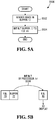
- graphics adapter driver software 108 within memory 16 performs steps S 500 depicted in FIG. 5A .
- driver software 108 generates commands directing graphics processor 54 to render the secondary adapter buffer 72 of memory 56 , in steps S 502 . These commands are placed in the command queue 57 of adapter 52 and executed by graphics processor 54 , in much the same way as commands would be queued in queue 47 , as described above.
- driver software 108 further generates a command (or commands) causing processor 54 to bit block transfer (BITBLT) the contents of secondary adapter frame buffer 72 within memory 56 in step S 504 , to that area of memory 16 allocated as frame buffer 46 for graphics adapter 34 .
- BITBLT bit block transfer
- Display interface 44 of graphics adapter 34 has been preprogrammed to display the contents of its frame buffer 46 to an interconnected monitor or display at port 48 . Conveniently then, images displayed on displays 32 and 68 interconnected with ports 48 and port 64 are rendered or drawn by graphics processor 54 . The effects of step S 504 on buffer 72 and frame buffer 46 is illustrated in FIG. 5 B .
- steps S 600 depicted in FIG. 6 A are performed.
- front and back frame buffers are allocated within memory 16 of adapter 52 .
- buffers 46 a and 46 b are designated as buffers 46 a and 46 b, and depicted in FIG. 6 B .
- Processor 54 again renders any frame to presented by display interface 44 within secondary adapter frame buffer 72 of memory 56 as described above with reference to step S 502 , in step S 602 .
- driver software 108 programs graphics processor 54 to bit block transfer (BITBLT) the contents of secondary adapter frame buffer 72 within memory 56 , to the then current back buffer within memory 16 for graphics adapter 34 in step S 604 .
- BITBLT bit block transfer
- Display interface 44 of graphics adapter 34 presents the contents of it's the buffer to an interconnected monitor (i.e.
- step S 604 Driver software 108 , of course, maintains the start location and status of each buffers 46 a and 46 b as front and back buffers.
- steps S 604 and S 606 on buffers 46 a and 46 b is schematically illustrated in FIG. 6 B .
- a single buffer 46 or direct programming of display interface 44 of adapter 34 may cause visible tearing. That is, any time outside of the vertical blanking interval that registers of display interface 44 are reprogrammed, tearing may be visible, as display parameters are changed in the middle of the frame output by interface 44 .
- steps S 700 depicted in FIG. 7 may be performed.
- front and rear buffers 46 a, 46 b are initially allocated within memory 16 used by adapter 34 .
- Processor 54 again renders images for display at device 32 within buffer 72 of local memory 56 , as described above with reference to steps S 502 and S 602 .
- driver software 108 within memory 16 programs graphics processor 54 to bit block transfer (BITBLT) the contents of secondary adapter frame buffer 72 within memory 56 , to the then current back buffer within memory 16 of graphics adapter 34 in step S 704 .
- Driver software 108 further places a command in the command queue 47 of adapter 34 to flip front and back buffers, in step S 706 .
- registers of command processor 42 are not updated by driver software 108 to reflect the pending command in command queue 47 . Instead, driver software 108 provides a command to graphics processor 54 in step S 708 to update command queue registers of command processor 42 upon completion of the bit block transfer initiated in step S 706 .
- command processor 42 causes command processor 42 to provide instructions to processor 40 to flip its back to front buffer.
- Graphics processor 40 executes the queued command to flip back and front buffers of adapter 34 (i.e. by reprogramming registers of display interface 44 to present the contents of its previous back buffer to an interconnected monitor or display at port 48 ).
- steps S 800 depicted in FIG. 8 are performed. Again, front and back buffers are initially allocated within memory 16 of adapter 34 . Processor 54 again renders images for display 32 within buffer 72 of local memory 56 , as described above.
- Driver software 108 further places a command in queue 47 of adapter 34 to cause graphics processor 40 to bit block transfer (BITBLT) the contents of the secondary frame buffer 72 within memory 56 , to that area of system memory 16 allocated as the current back frame buffer for graphics adapter 34 .
- Driver software 108 also places a command in queue 47 to cause graphics processor 40 to flip front and back buffers of adapter 34 by programming display interface 44 to use the rear buffer as front buffer.
- registers of command processor 42 defining the queue pointer are not updated until a frame has been rendered in buffer 72 .
- graphics processor 54 provides a command to update command registers defining the queue pointer for command processor 42 to reflect the two pending commands within the command queue of adapter 34 .
- Graphics processor 40 executes the queued commands to bit block transfer the contents of buffer 72 to its back buffer and flip its back and front buffers (i.e. by reprogramming registers of display interface 44 to present the contents of its previous back buffer to an interconnected monitor or display at port 48 ).
- a slave graphics adapter may be used to display images created in one frame buffer.
- Device electronics and ports required to drive additional displays may be provided by slave graphics adapter 34 .
- electronics included in the slave graphics controller may be effectively utilized to allow driving of multiple displays.
- buffers 70 and 72 may be used to define a single surface on which application software 106 may render single graphic images to be displayed across two or more displays 48 and 64 , interconnected with graphics adapters 52 and 34 .
- Driver software 108 may accordingly report an available screen size to application software 106 , equal to the size of buffer 70 and buffer 72 .
- buffer 70 has a resolution of m.sub. 1 xn
- buffer 72 has a resolution of m.sub. 2 xn
- driver software 108 may report an available screen size of (m.sub. 1 +m.sub. 2 )xn to an application of application software 106 .
- Rendering by driver software 108 is simplified if buffers 70 and 72 occupy adjacent (m.sub. 1 +m.sub.
- Application software 106 may, in turn use driver software 108 to cause graphics processor 40 to render larger images having a resolution of (m.sub. 1 +m.sub. 2 )xn pixels making up the surface defined by buffers 70 and 72 .
- Buffers 70 and 72 thus store image pairs, with each image of the pair forming a portion of the larger image rendered by the application.
- driver software 108 may transfer the image in buffer 72 to frame buffer 46 , for display on display 32 , in accordance with steps S 500 , S 600 , S 700 or S 800 described above.
- the image in buffer 70 may be displayed on display 68 in normal fashion.
- An end user viewing displays 32 and 68 side by side recognizes the larger image rendered by application 106 .
- application 106 in the form of a game may take advantage of multiple displays, without requiring modification.
- Steps S 602 , S 604 , S 702 , S 704 , or steps S 802 , S 704 could accordingly be modified to bit block transfer the buffer holding the just completed image to the back buffer 46 a or 46 b.
- existing application software 106 need not be modified. Instead, the application software may simply rely on the reported larger screen size.
- Driver software 108 causes the rendering of surfaces across multiple displays.
- the slave graphics adapter could easily be another graphics adapter in communication with graphics adapter 52 by way of a bus having sufficient bandwidth to allow transfer of graphics frames into the slave frame buffer(s).
- the slave graphics processor could be formed as another PCle compliant expansion card. So, for example, as graphics cards are upgraded, older expansion cards may still be used for their ability to drive interconnected displays.
- the interconnect bus need not be a PCle interconnect bus, but could be any other suitable bus having a bandwidth allowing transfer of data between frame buffers at a rate equal to the refresh rate used by display interface 44 .
- frame buffers 46 and front and back buffers 46 a and 46 b
- frame buffers 46 have been described as being formed in system memory 16 , they could easily be formed as part of memory local to adapter 34 .
- rendering across bus 22 may allow a graphics adapter (or subsystem) interconnected by high speed bus 22 to take the place of an integrated adapter/subsystem.
- FIG. 9 is a simplified block diagrams exemplary of a portion of a computing device 10' exemplary of another embodiment.
- Computing device 10' is detailed in US Patent Application No. 11/421,005 .
- device 10' includes two graphics subsystem 30' and 40' .
- Graphics subsystem 30' includes a graphics engine/processor 32' , a memory controller 72' , a display interface 74' and a bus interface 78' .
- a second graphics subsystem 40' is in communication with graphics subsystem 30' , by way of high speed bus 22' , such as the PCle bus .
- Graphics subsystem 40' includes its own graphics engine/processor 42' ; memory controller 52' ; display interface 54' .
- Graphics subsystem 40' is further in communication with graphics memory 50' .
- subsystem 40' is adapted to render graphics to memory 14' , across bus 22' .
- Device 10' may conveniently be formed as a portable computing device in the form of a laptop or smaller computing device.
- a single housing may contain a DC power source, display 26' and the above mentioned motherboard and components.
- the second graphics subsystem 40' may be added to a single housing that houses the remainder of the computing device, or may form part of a docking station that only forms part of device 10' , when device 10' is physically interconnected thereto.
- Device 10' may be operated in at least two power consumption modes: a higher power consumption mode and a lower power consumption mode.
- the higher power mode may be assumed when device 10' is powered by a power source connected to an AC(mains) supply; the lower power consumption mode may be assumed when device 10' is powered by a DC power source using one or more batteries, fuel cells, or the like.
- power consumption modes may be user selected, software controlled, based on for example, user preferences, types of software applications being executed, battery levels, and the like, or otherwise chosen.
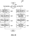
- FIG. 10 depicts software blocks S800' , that may be performed by a central processor (like processor 12 - FIG. 1 ) under control of software within system memory of device 10' .
- Blocks S800' may be performed each time device 10' undergoes a state change, for which subsystems 30' and 40' should be configured accordingly.
- the software determines whether device 10' should assume its higher power consumption mode, or its lower power consumption mode.
- blocks S804'-S810' are executed.
- graphics subsystem 40' is placed in its full operational (high power consumption) mode, if it is not already in this mode. This may be performed by providing an appropriate signal to power controller 60' , through the driver controlling graphics subsystem 40' .
- graphics subsystem 40' is enabled in blocks S806 and S808 . Again, this may be performed by logically disabling any display interconnected associated with graphics subsystem 30' in block S804 , and logically enabling the display connected with graphics subsystem 40' , in block S808 .
- Blocks S806 and S808 may again be performed, by appropriate operating system API calls, such as the EnumDisplayDevices() and ChangeDisplaySettingsEX() calls described in the 11/421,005 patent application, or through direct communication with hardware.
- graphics subsystem 40' no physical display is connected to graphics subsystem 40' .
- Driver software controlling operation of graphics subsystem 40' is configured to render images in buffer 14' of graphics subsystem 30' instead of within associated memory 50' in step S810' .
- high speed bus 22' embodied, for example, as the PCle bus
- rendering is possible across bus 22' , owing in part to transfer speeds enabled by the bus.
- the rendering may be direct into the frame buffer across the bus, primitive by primitive, thus transferring the rendered image across bus 22' . This may be facilitated by allocating buffer 14' in memory accessible by subsystem 40' and providing the driver software for subsystem 40' with the address of buffer 14' . Alternatively, as will become apparent, the frames may be rendered in one buffer, and transferred by direct memory access or the like across bus 22' .
- the driver for graphics subsystem 30' is further configured to cause display interface 74' of graphics subsystem 30' to sample the frame buffer in memory 14' , so as to present the image rendered by graphics subsystem 40' in the frame buffer in memory 14' at interconnected display 26' .
- the driver for graphics subsystem 30' may direct graphics engine 32' of graphics subsystem 30' to remain substantially dormant or idle. This mode of operation is schematically depicted in FIG. 11A with only the active blocks of graphics subsystem 40' and graphics subsystem 30' , crosshatched.
- memory 50' and display interface 54' are not used. As such, these functional blocks could be eliminated from subsystem 40' allowing cost reduction.
- the resulting subsystem 40' need not include a display interface and would lack memory defining a frame buffer local to subsystem 40' .
- Producing such a graphics subsystem may be beneficial, as subsystem 40' could be produced to complement the functionality provided by subsystem 30' .
- subsystem could provide a graphics engine 42' that provides 3 D graphics or video decoding capabilities. Graphics engine 32' may not include these capabilities.
- 2 D graphics abilities offered by graphics engine 32' need not be included in subsystem 40' . Consumers, in turn could add graphics subsystem 30' only when additional functionality is needed.
- blocks S812' - S818' are executed.
- graphics subsystem 40' is partially or completely disabled and placed in its low power consumption mode, and rendering is again performed by graphics subsystem 30' .
- any display interconnected associated with graphics subsystem 30' may be enabled in block S812'
- any display physically connected with graphics subsystem 40' may be logically disabled in block S814' .
- driver software controlling operation of graphics subsystem 30' is again configured to cause graphics subsystem 30' to render images in memory 14' .
- Display interface 74' continues to sample memory 14' to present images on display 26' interconnected with port 78' .
- processor 12' first provides a suitable signal to power controller 60' in block S818' , placing graphics subsystem 40' in its low power state.
- a power controller (not shown) disconnects power to graphics subsystem 40' or places graphics subsystem 40' into a lower power sleep mode.
- voltages are throttled, and/or all or parts of graphics subsystem 40' are powered down and/or selected clocks used by graphics subsystem 40' are slowed.
- the graphics engine 42' of graphics subsystem 40' remains idle or substantially idle (e.g. it may be slowed, disable or powered down).
- This mode of operation is schematically depicted in FIG. 9B with only the active functional blocks of adapter 40' and graphics subsystem 30' , crosshatched.
- the inactive/idle functional blocks may be entirely disabled, or operated at reduced voltages or clock speeds.
- portions of graphics subsystem 30' could be disabled when graphics engine 32' is not in use. This could be facilitated by placing graphics engine 32' and other components on one or more voltage islands that may be disabled by way of a GPIO or similar circuit, any time graphics subsystem 40' is responsible for rendering images.
- both graphics subsystem 30' and graphics subsystem 40' could render to memory 14' or memory 50' .
- the two graphics subsystems 30' and 40' may operate in concert, each rendering an alternate frame in memory 14' or rendering an alternate portion (e.g. scan-line) of each frame in memory 14' .
- additional displays may be connected to graphics subsystems 30' and 40' allowing concurrent use of multiple displays in the high power consumption modes, as detailed above.
- display interface 54' could be used to drive a second display.
- device 10' Upon transition to a lower power consumption mode, device 10' could be configured to operate as depicted in FIG. 11B .
- device 10' could include multiple additional graphics subsystems connected to bus 22' (or 22 ), all of which could be active in the high power consumption mode, and render graphics through display interface 74' of graphics subsystem 30' . Upon transition to the lower power consumption mode, these could be disabled and rendering could be left to graphics engine 32' of graphics subsystem 30' .
- computing device 10' may include a direct memory access (DMA) controller 90 .
- DMA controller 90 may transfer data from memory 50' to memory 14' .
- graphics subsystem 40' could render images to memory 50' . These rendered images could then be transferred by DMA controller 90 to a frame buffer in memory 14' .
- DMA controller 90' could form part of graphics subsystem 30' or 40' (for example as DMA engines of graphics engines 32' or 42' ), or be otherwise located in computing device 10' .
- Data may be transferred across bus 20' or otherwise directly from memory 50' to memory 14' .
- Display interface 74' would continue operating as disclosed above, sampling the frame buffer in memory 14' to present the rendered image on display 26' .
- active blocks of device 10' of FIG. 10 in its higher power consumption mode are illustrated in crosshatch in FIG. 12 .
Landscapes
- Engineering & Computer Science (AREA)
- Theoretical Computer Science (AREA)
- Physics & Mathematics (AREA)
- General Physics & Mathematics (AREA)
- Computer Hardware Design (AREA)
- Computer Graphics (AREA)
- Human Computer Interaction (AREA)
- General Engineering & Computer Science (AREA)
- Controls And Circuits For Display Device (AREA)
- Digital Computer Display Output (AREA)
- Information Transfer Systems (AREA)
Applications Claiming Priority (2)
| Application Number | Priority Date | Filing Date | Title |
|---|---|---|---|
| US11/987,559 US20080143731A1 (en) | 2005-05-24 | 2007-11-30 | Video rendering across a high speed peripheral interconnect bus |
| PCT/US2008/085160 WO2009073617A1 (en) | 2007-11-30 | 2008-12-01 | Video rendering across a high speed peripheral interconnect bus |
Publications (2)
| Publication Number | Publication Date |
|---|---|
| EP2225752A1 EP2225752A1 (en) | 2010-09-08 |
| EP2225752B1 true EP2225752B1 (en) | 2016-03-23 |
Family
ID=40383655
Family Applications (1)
| Application Number | Title | Priority Date | Filing Date |
|---|---|---|---|
| EP08856301.0A Active EP2225752B1 (en) | 2007-11-30 | 2008-12-01 | Video rendering across a high speed peripheral interconnect bus |
Country Status (6)
| Country | Link |
|---|---|
| US (1) | US20080143731A1 (ja) |
| EP (1) | EP2225752B1 (ja) |
| JP (1) | JP5529748B2 (ja) |
| KR (1) | KR101545682B1 (ja) |
| CN (2) | CN101965610A (ja) |
| WO (1) | WO2009073617A1 (ja) |
Families Citing this family (27)
| Publication number | Priority date | Publication date | Assignee | Title |
|---|---|---|---|---|
| US7961194B2 (en) | 2003-11-19 | 2011-06-14 | Lucid Information Technology, Ltd. | Method of controlling in real time the switching of modes of parallel operation of a multi-mode parallel graphics processing subsystem embodied within a host computing system |
| US8085273B2 (en) | 2003-11-19 | 2011-12-27 | Lucid Information Technology, Ltd | Multi-mode parallel graphics rendering system employing real-time automatic scene profiling and mode control |
| US7777748B2 (en) | 2003-11-19 | 2010-08-17 | Lucid Information Technology, Ltd. | PC-level computing system with a multi-mode parallel graphics rendering subsystem employing an automatic mode controller, responsive to performance data collected during the run-time of graphics applications |
| CN1890660A (zh) | 2003-11-19 | 2007-01-03 | 路西德信息技术有限公司 | Pc总线上的多重三维图形管线的方法及系统 |
| US20090027383A1 (en) | 2003-11-19 | 2009-01-29 | Lucid Information Technology, Ltd. | Computing system parallelizing the operation of multiple graphics processing pipelines (GPPLs) and supporting depth-less based image recomposition |
| US8497865B2 (en) * | 2006-12-31 | 2013-07-30 | Lucid Information Technology, Ltd. | Parallel graphics system employing multiple graphics processing pipelines with multiple graphics processing units (GPUS) and supporting an object division mode of parallel graphics processing using programmable pixel or vertex processing resources provided with the GPUS |
| CA2595085A1 (en) * | 2005-01-25 | 2006-11-09 | Lucid Information Technology, Ltd. | Graphics processing and display system employing multiple graphics cores on a silicon chip of monolithic construction |
| US7861013B2 (en) * | 2007-12-13 | 2010-12-28 | Ati Technologies Ulc | Display system with frame reuse using divided multi-connector element differential bus connector |
| US8890876B1 (en) * | 2007-12-21 | 2014-11-18 | Oracle America, Inc. | Microprocessor including a display interface in the microprocessor |
| US9336752B1 (en) * | 2007-12-21 | 2016-05-10 | Oracle America, Inc. | Microprocessor including a display interface in the microprocessor |
| CN101639930B (zh) * | 2008-08-01 | 2012-07-04 | 辉达公司 | 一连串绘图处理器处理绘图数据的方法及系统 |
| US9324294B2 (en) * | 2009-04-07 | 2016-04-26 | Nvidia Corporation | Graphics system for supporting multiple digital display interface standards |
| US8316255B2 (en) * | 2009-09-09 | 2012-11-20 | Ati Technologies Ulc | Method and apparatus for responding to signals from a disabling device while in a disabled state |
| US8482574B2 (en) * | 2009-10-06 | 2013-07-09 | Nvidia Corporation | System, method, and computer program product for calculating statistics associated with a surface to be rendered utilizing a graphics processor |
| US20110090234A1 (en) * | 2009-10-19 | 2011-04-21 | Barnes & Noble, Inc. | Apparatus and method for control of multiple displays from a single virtual frame buffer |
| US8760459B2 (en) * | 2009-12-30 | 2014-06-24 | Intel Corporation | Display data management techniques |
| US8963797B2 (en) * | 2010-01-06 | 2015-02-24 | Apple Inc. | Display driving architectures |
| JP2011141707A (ja) | 2010-01-07 | 2011-07-21 | Sony Corp | 情報処理装置、情報処理方法及びプログラム |
| US8659616B2 (en) * | 2010-02-18 | 2014-02-25 | Nvidia Corporation | System, method, and computer program product for rendering pixels with at least one semi-transparent surface |
| JP2011188364A (ja) * | 2010-03-10 | 2011-09-22 | Xgi Technology Inc | 多画面信号処理装置及び多画面システム |
| US20110242115A1 (en) * | 2010-03-30 | 2011-10-06 | You-Ming Tsao | Method for performing image signal processing with aid of a graphics processing unit, and associated apparatus |
| US9164646B2 (en) * | 2010-08-31 | 2015-10-20 | Ati Technologies Ulc | Method and apparatus for accommodating display migration among a plurality of physical displays |
| US10817043B2 (en) * | 2011-07-26 | 2020-10-27 | Nvidia Corporation | System and method for entering and exiting sleep mode in a graphics subsystem |
| US9251552B2 (en) * | 2012-06-28 | 2016-02-02 | Intel Corporation | Method and apparatus for managing image data for presentation on a display |
| CN105389768B (zh) * | 2015-10-21 | 2019-06-28 | 努比亚技术有限公司 | 图片处理方法及装置 |
| JP2017097066A (ja) * | 2015-11-19 | 2017-06-01 | ルネサスエレクトロニクス株式会社 | 画像処理装置及び画像処理方法 |
| US11074666B2 (en) * | 2019-01-30 | 2021-07-27 | Sony Interactive Entertainment LLC | Scalable game console CPU/GPU design for home console and cloud gaming |
Citations (3)
| Publication number | Priority date | Publication date | Assignee | Title |
|---|---|---|---|---|
| US5896141A (en) * | 1996-07-26 | 1999-04-20 | Hewlett-Packard Company | System and method for virtual device access in a computer system |
| US20050237327A1 (en) * | 2004-04-23 | 2005-10-27 | Nvidia Corporation | Point-to-point bus bridging without a bridge controller |
| US20050285863A1 (en) * | 2004-06-25 | 2005-12-29 | Diamond Michael B | Discrete graphics system unit for housing a GPU |
Family Cites Families (33)
| Publication number | Priority date | Publication date | Assignee | Title |
|---|---|---|---|---|
| JPH0727556B2 (ja) * | 1990-02-09 | 1995-03-29 | 富士通株式会社 | バスアクセス方式 |
| US5485562A (en) * | 1993-09-14 | 1996-01-16 | International Business Machines Corporation | System and method for clipping pixels drawn in one of plurality of windows in a computer graphics system |
| US5712664A (en) * | 1993-10-14 | 1998-01-27 | Alliance Semiconductor Corporation | Shared memory graphics accelerator system |
| US5488385A (en) * | 1994-03-03 | 1996-01-30 | Trident Microsystems, Inc. | Multiple concurrent display system |
| JPH0922339A (ja) * | 1995-07-05 | 1997-01-21 | Matsushita Electric Ind Co Ltd | 遠隔操作装置 |
| WO1998032068A1 (en) * | 1997-01-17 | 1998-07-23 | Intergraph Corporation | Multiple display synchronization apparatus and method |
| US6018340A (en) * | 1997-01-27 | 2000-01-25 | Microsoft Corporation | Robust display management in a multiple monitor environment |
| US5949437A (en) * | 1997-02-19 | 1999-09-07 | Appian Graphics Corp. | Dual video output board with a shared memory interface |
| US6104414A (en) * | 1997-03-12 | 2000-08-15 | Cybex Computer Products Corporation | Video distribution hub |
| JPH1165719A (ja) * | 1997-08-21 | 1999-03-09 | Toshiba Corp | コンピュータおよび画像表示方法 |
| JPH11109937A (ja) * | 1997-09-29 | 1999-04-23 | Casio Comput Co Ltd | 表示制御装置 |
| US6040845A (en) * | 1997-12-22 | 2000-03-21 | Compaq Computer Corp. | Device and method for reducing power consumption within an accelerated graphics port target |
| US6208361B1 (en) * | 1998-06-15 | 2001-03-27 | Silicon Graphics, Inc. | Method and system for efficient context switching in a computer graphics system |
| US6532019B1 (en) * | 1998-06-17 | 2003-03-11 | Advanced Micro Devices, Inc. | Input/output integrated circuit hub incorporating a RAMDAC |
| US6573905B1 (en) * | 1999-11-09 | 2003-06-03 | Broadcom Corporation | Video and graphics system with parallel processing of graphics windows |
| US6624816B1 (en) * | 1999-09-10 | 2003-09-23 | Intel Corporation | Method and apparatus for scalable image processing |
| US6760031B1 (en) * | 1999-12-31 | 2004-07-06 | Intel Corporation | Upgrading an integrated graphics subsystem |
| US20030158886A1 (en) * | 2001-10-09 | 2003-08-21 | Walls Jeffrey J. | System and method for configuring a plurality of computers that collectively render a display |
| US7079149B2 (en) * | 2001-10-09 | 2006-07-18 | Texas Instruments Incorporated | System, method, and device for accelerated graphics port linking |
| US6864891B2 (en) * | 2002-01-31 | 2005-03-08 | Hewlett-Packard Development Company L.P. | Switching between internal and external display adapters in a portable computer system |
| US6700580B2 (en) * | 2002-03-01 | 2004-03-02 | Hewlett-Packard Development Company, L.P. | System and method utilizing multiple pipelines to render graphical data |
| US6886057B2 (en) * | 2002-06-06 | 2005-04-26 | Dell Products L.P. | Method and system for supporting multiple bus protocols on a set of wirelines |
| US7102645B2 (en) * | 2003-12-15 | 2006-09-05 | Seiko Epson Corporation | Graphics display controller providing enhanced read/write efficiency for interfacing with a RAM-integrated graphics display device |
| US7289125B2 (en) * | 2004-02-27 | 2007-10-30 | Nvidia Corporation | Graphics device clustering with PCI-express |
| US7265759B2 (en) * | 2004-04-09 | 2007-09-04 | Nvidia Corporation | Field changeable rendering system for a computing device |
| US20050237329A1 (en) * | 2004-04-27 | 2005-10-27 | Nvidia Corporation | GPU rendering to system memory |
| JP2005316176A (ja) * | 2004-04-28 | 2005-11-10 | Toshiba Corp | 電子機器及び表示制御方法 |
| TWM261751U (en) * | 2004-07-09 | 2005-04-11 | Uniwill Comp Corp | Switching display processing architecture for information device |
| US7721118B1 (en) * | 2004-09-27 | 2010-05-18 | Nvidia Corporation | Optimizing power and performance for multi-processor graphics processing |
| US7545380B1 (en) * | 2004-12-16 | 2009-06-09 | Nvidia Corporation | Sequencing of displayed images for alternate frame rendering in a multi-processor graphics system |
| US7730336B2 (en) * | 2006-05-30 | 2010-06-01 | Ati Technologies Ulc | Device having multiple graphics subsystems and reduced power consumption mode, software and methods |
| US7817155B2 (en) * | 2005-05-24 | 2010-10-19 | Ati Technologies Inc. | Master/slave graphics adapter arrangement |
| US7698579B2 (en) * | 2006-08-03 | 2010-04-13 | Apple Inc. | Multiplexed graphics architecture for graphics power management |
-
2007
- 2007-11-30 US US11/987,559 patent/US20080143731A1/en not_active Abandoned
-
2008
- 2008-12-01 JP JP2010536221A patent/JP5529748B2/ja active Active
- 2008-12-01 CN CN2008801258634A patent/CN101965610A/zh active Pending
- 2008-12-01 CN CN201710860732.1A patent/CN107845374B/zh active Active
- 2008-12-01 EP EP08856301.0A patent/EP2225752B1/en active Active
- 2008-12-01 WO PCT/US2008/085160 patent/WO2009073617A1/en active Application Filing
- 2008-12-01 KR KR1020107014602A patent/KR101545682B1/ko active IP Right Grant
Patent Citations (3)
| Publication number | Priority date | Publication date | Assignee | Title |
|---|---|---|---|---|
| US5896141A (en) * | 1996-07-26 | 1999-04-20 | Hewlett-Packard Company | System and method for virtual device access in a computer system |
| US20050237327A1 (en) * | 2004-04-23 | 2005-10-27 | Nvidia Corporation | Point-to-point bus bridging without a bridge controller |
| US20050285863A1 (en) * | 2004-06-25 | 2005-12-29 | Diamond Michael B | Discrete graphics system unit for housing a GPU |
Also Published As
| Publication number | Publication date |
|---|---|
| CN101965610A (zh) | 2011-02-02 |
| JP2011509445A (ja) | 2011-03-24 |
| US20080143731A1 (en) | 2008-06-19 |
| CN107845374B (zh) | 2021-10-01 |
| WO2009073617A1 (en) | 2009-06-11 |
| KR20100114496A (ko) | 2010-10-25 |
| KR101545682B1 (ko) | 2015-08-19 |
| JP5529748B2 (ja) | 2014-06-25 |
| CN107845374A (zh) | 2018-03-27 |
| EP2225752A1 (en) | 2010-09-08 |
Similar Documents
| Publication | Publication Date | Title |
|---|---|---|
| EP2225752B1 (en) | Video rendering across a high speed peripheral interconnect bus | |
| US7817155B2 (en) | Master/slave graphics adapter arrangement | |
| US7730336B2 (en) | Device having multiple graphics subsystems and reduced power consumption mode, software and methods | |
| TWI466099B (zh) | 支援耦接至圖形控制器的自更新顯示器的方法和裝置 | |
| EP2515294B1 (en) | Method and apparatus to support a self-refreshing display device coupled to a graphics controller | |
| JP5427187B2 (ja) | 複数のグラフィックサブシステムおよび低電力消費モードを有するコンピューティングデバイス用ドライバアーキテクチャ、ソフトウェアおよび方法 | |
| US7750912B2 (en) | Integrating display controller into low power processor | |
| US20100321395A1 (en) | Display simulation system and method | |
| US8612652B2 (en) | Systems, methods, and media for disabling graphic processing units | |
| US6734862B1 (en) | Memory controller hub | |
| EP2426660A1 (en) | Method and apparatus for optimizing data flow in a graphics co-processor | |
| US10228750B2 (en) | Reducing the power consumption of an information handling system capable of handling both dynamic and static display applications | |
| CN117099070A (zh) | 基于利用的电源的图形处理单元(gpu)选择 | |
| CN117078499B (zh) | 双显卡渲染处理方法、装置、计算设备及可读存储介质 | |
| Perfetto | A Low Power Touch Screen Document Viewer |
Legal Events
| Date | Code | Title | Description |
|---|---|---|---|
| PUAI | Public reference made under article 153(3) epc to a published international application that has entered the european phase |
Free format text: ORIGINAL CODE: 0009012 |
|
| 17P | Request for examination filed |
Effective date: 20100629 |
|
| AK | Designated contracting states |
Kind code of ref document: A1 Designated state(s): AT BE BG CH CY CZ DE DK EE ES FI FR GB GR HR HU IE IS IT LI LT LU LV MC MT NL NO PL PT RO SE SI SK TR |
|
| AX | Request for extension of the european patent |
Extension state: AL BA MK RS |
|
| DAX | Request for extension of the european patent (deleted) | ||
| 17Q | First examination report despatched |
Effective date: 20111116 |
|
| RIC1 | Information provided on ipc code assigned before grant |
Ipc: G09G 5/397 20060101ALI20150805BHEP Ipc: G06T 1/20 20060101ALI20150805BHEP Ipc: G09G 5/395 20060101ALI20150805BHEP Ipc: G09G 5/36 20060101AFI20150805BHEP |
|
| GRAP | Despatch of communication of intention to grant a patent |
Free format text: ORIGINAL CODE: EPIDOSNIGR1 |
|
| INTG | Intention to grant announced |
Effective date: 20150923 |
|
| GRAS | Grant fee paid |
Free format text: ORIGINAL CODE: EPIDOSNIGR3 |
|
| GRAA | (expected) grant |
Free format text: ORIGINAL CODE: 0009210 |
|
| AK | Designated contracting states |
Kind code of ref document: B1 Designated state(s): AT BE BG CH CY CZ DE DK EE ES FI FR GB GR HR HU IE IS IT LI LT LU LV MC MT NL NO PL PT RO SE SI SK TR |
|
| REG | Reference to a national code |
Ref country code: GB Ref legal event code: FG4D |
|
| REG | Reference to a national code |
Ref country code: CH Ref legal event code: EP |
|
| REG | Reference to a national code |
Ref country code: AT Ref legal event code: REF Ref document number: 783818 Country of ref document: AT Kind code of ref document: T Effective date: 20160415 |
|
| REG | Reference to a national code |
Ref country code: IE Ref legal event code: FG4D |
|
| REG | Reference to a national code |
Ref country code: DE Ref legal event code: R096 Ref document number: 602008043104 Country of ref document: DE |
|
| REG | Reference to a national code |
Ref country code: LT Ref legal event code: MG4D |
|
| REG | Reference to a national code |
Ref country code: NL Ref legal event code: MP Effective date: 20160323 |
|
| PG25 | Lapsed in a contracting state [announced via postgrant information from national office to epo] |
Ref country code: GR Free format text: LAPSE BECAUSE OF FAILURE TO SUBMIT A TRANSLATION OF THE DESCRIPTION OR TO PAY THE FEE WITHIN THE PRESCRIBED TIME-LIMIT Effective date: 20160624 Ref country code: NO Free format text: LAPSE BECAUSE OF FAILURE TO SUBMIT A TRANSLATION OF THE DESCRIPTION OR TO PAY THE FEE WITHIN THE PRESCRIBED TIME-LIMIT Effective date: 20160623 Ref country code: FI Free format text: LAPSE BECAUSE OF FAILURE TO SUBMIT A TRANSLATION OF THE DESCRIPTION OR TO PAY THE FEE WITHIN THE PRESCRIBED TIME-LIMIT Effective date: 20160323 |
|
| REG | Reference to a national code |
Ref country code: AT Ref legal event code: MK05 Ref document number: 783818 Country of ref document: AT Kind code of ref document: T Effective date: 20160323 |
|
| PG25 | Lapsed in a contracting state [announced via postgrant information from national office to epo] |
Ref country code: LT Free format text: LAPSE BECAUSE OF FAILURE TO SUBMIT A TRANSLATION OF THE DESCRIPTION OR TO PAY THE FEE WITHIN THE PRESCRIBED TIME-LIMIT Effective date: 20160323 Ref country code: LV Free format text: LAPSE BECAUSE OF FAILURE TO SUBMIT A TRANSLATION OF THE DESCRIPTION OR TO PAY THE FEE WITHIN THE PRESCRIBED TIME-LIMIT Effective date: 20160323 Ref country code: NL Free format text: LAPSE BECAUSE OF FAILURE TO SUBMIT A TRANSLATION OF THE DESCRIPTION OR TO PAY THE FEE WITHIN THE PRESCRIBED TIME-LIMIT Effective date: 20160323 Ref country code: SE Free format text: LAPSE BECAUSE OF FAILURE TO SUBMIT A TRANSLATION OF THE DESCRIPTION OR TO PAY THE FEE WITHIN THE PRESCRIBED TIME-LIMIT Effective date: 20160323 |
|
| PG25 | Lapsed in a contracting state [announced via postgrant information from national office to epo] |
Ref country code: IS Free format text: LAPSE BECAUSE OF FAILURE TO SUBMIT A TRANSLATION OF THE DESCRIPTION OR TO PAY THE FEE WITHIN THE PRESCRIBED TIME-LIMIT Effective date: 20160723 Ref country code: PL Free format text: LAPSE BECAUSE OF FAILURE TO SUBMIT A TRANSLATION OF THE DESCRIPTION OR TO PAY THE FEE WITHIN THE PRESCRIBED TIME-LIMIT Effective date: 20160323 Ref country code: EE Free format text: LAPSE BECAUSE OF FAILURE TO SUBMIT A TRANSLATION OF THE DESCRIPTION OR TO PAY THE FEE WITHIN THE PRESCRIBED TIME-LIMIT Effective date: 20160323 |
|
| PG25 | Lapsed in a contracting state [announced via postgrant information from national office to epo] |
Ref country code: AT Free format text: LAPSE BECAUSE OF FAILURE TO SUBMIT A TRANSLATION OF THE DESCRIPTION OR TO PAY THE FEE WITHIN THE PRESCRIBED TIME-LIMIT Effective date: 20160323 Ref country code: PT Free format text: LAPSE BECAUSE OF FAILURE TO SUBMIT A TRANSLATION OF THE DESCRIPTION OR TO PAY THE FEE WITHIN THE PRESCRIBED TIME-LIMIT Effective date: 20160725 Ref country code: SK Free format text: LAPSE BECAUSE OF FAILURE TO SUBMIT A TRANSLATION OF THE DESCRIPTION OR TO PAY THE FEE WITHIN THE PRESCRIBED TIME-LIMIT Effective date: 20160323 Ref country code: RO Free format text: LAPSE BECAUSE OF FAILURE TO SUBMIT A TRANSLATION OF THE DESCRIPTION OR TO PAY THE FEE WITHIN THE PRESCRIBED TIME-LIMIT Effective date: 20160323 Ref country code: CZ Free format text: LAPSE BECAUSE OF FAILURE TO SUBMIT A TRANSLATION OF THE DESCRIPTION OR TO PAY THE FEE WITHIN THE PRESCRIBED TIME-LIMIT Effective date: 20160323 Ref country code: ES Free format text: LAPSE BECAUSE OF FAILURE TO SUBMIT A TRANSLATION OF THE DESCRIPTION OR TO PAY THE FEE WITHIN THE PRESCRIBED TIME-LIMIT Effective date: 20160323 |
|
| PG25 | Lapsed in a contracting state [announced via postgrant information from national office to epo] |
Ref country code: BE Free format text: LAPSE BECAUSE OF FAILURE TO SUBMIT A TRANSLATION OF THE DESCRIPTION OR TO PAY THE FEE WITHIN THE PRESCRIBED TIME-LIMIT Effective date: 20160323 Ref country code: IT Free format text: LAPSE BECAUSE OF FAILURE TO SUBMIT A TRANSLATION OF THE DESCRIPTION OR TO PAY THE FEE WITHIN THE PRESCRIBED TIME-LIMIT Effective date: 20160323 |
|
| REG | Reference to a national code |
Ref country code: DE Ref legal event code: R097 Ref document number: 602008043104 Country of ref document: DE |
|
| PLBE | No opposition filed within time limit |
Free format text: ORIGINAL CODE: 0009261 |
|
| STAA | Information on the status of an ep patent application or granted ep patent |
Free format text: STATUS: NO OPPOSITION FILED WITHIN TIME LIMIT |
|
| PG25 | Lapsed in a contracting state [announced via postgrant information from national office to epo] |
Ref country code: DK Free format text: LAPSE BECAUSE OF FAILURE TO SUBMIT A TRANSLATION OF THE DESCRIPTION OR TO PAY THE FEE WITHIN THE PRESCRIBED TIME-LIMIT Effective date: 20160323 |
|
| PG25 | Lapsed in a contracting state [announced via postgrant information from national office to epo] |
Ref country code: BG Free format text: LAPSE BECAUSE OF FAILURE TO SUBMIT A TRANSLATION OF THE DESCRIPTION OR TO PAY THE FEE WITHIN THE PRESCRIBED TIME-LIMIT Effective date: 20160623 |
|
| 26N | No opposition filed |
Effective date: 20170102 |
|
| PG25 | Lapsed in a contracting state [announced via postgrant information from national office to epo] |
Ref country code: SI Free format text: LAPSE BECAUSE OF FAILURE TO SUBMIT A TRANSLATION OF THE DESCRIPTION OR TO PAY THE FEE WITHIN THE PRESCRIBED TIME-LIMIT Effective date: 20160323 |
|
| REG | Reference to a national code |
Ref country code: CH Ref legal event code: PL |
|
| PG25 | Lapsed in a contracting state [announced via postgrant information from national office to epo] |
Ref country code: MC Free format text: LAPSE BECAUSE OF FAILURE TO SUBMIT A TRANSLATION OF THE DESCRIPTION OR TO PAY THE FEE WITHIN THE PRESCRIBED TIME-LIMIT Effective date: 20160323 |
|
| REG | Reference to a national code |
Ref country code: FR Ref legal event code: ST Effective date: 20170831 |
|
| REG | Reference to a national code |
Ref country code: IE Ref legal event code: MM4A |
|
| PG25 | Lapsed in a contracting state [announced via postgrant information from national office to epo] |
Ref country code: LI Free format text: LAPSE BECAUSE OF NON-PAYMENT OF DUE FEES Effective date: 20161231 Ref country code: LU Free format text: LAPSE BECAUSE OF NON-PAYMENT OF DUE FEES Effective date: 20161201 Ref country code: CH Free format text: LAPSE BECAUSE OF NON-PAYMENT OF DUE FEES Effective date: 20161231 Ref country code: FR Free format text: LAPSE BECAUSE OF NON-PAYMENT OF DUE FEES Effective date: 20170102 |
|
| PG25 | Lapsed in a contracting state [announced via postgrant information from national office to epo] |
Ref country code: IE Free format text: LAPSE BECAUSE OF NON-PAYMENT OF DUE FEES Effective date: 20161201 |
|
| PG25 | Lapsed in a contracting state [announced via postgrant information from national office to epo] |
Ref country code: CY Free format text: LAPSE BECAUSE OF FAILURE TO SUBMIT A TRANSLATION OF THE DESCRIPTION OR TO PAY THE FEE WITHIN THE PRESCRIBED TIME-LIMIT Effective date: 20160323 Ref country code: HU Free format text: LAPSE BECAUSE OF FAILURE TO SUBMIT A TRANSLATION OF THE DESCRIPTION OR TO PAY THE FEE WITHIN THE PRESCRIBED TIME-LIMIT; INVALID AB INITIO Effective date: 20081201 |
|
| PG25 | Lapsed in a contracting state [announced via postgrant information from national office to epo] |
Ref country code: HR Free format text: LAPSE BECAUSE OF FAILURE TO SUBMIT A TRANSLATION OF THE DESCRIPTION OR TO PAY THE FEE WITHIN THE PRESCRIBED TIME-LIMIT Effective date: 20160323 Ref country code: TR Free format text: LAPSE BECAUSE OF FAILURE TO SUBMIT A TRANSLATION OF THE DESCRIPTION OR TO PAY THE FEE WITHIN THE PRESCRIBED TIME-LIMIT Effective date: 20160323 |
|
| PG25 | Lapsed in a contracting state [announced via postgrant information from national office to epo] |
Ref country code: MT Free format text: LAPSE BECAUSE OF NON-PAYMENT OF DUE FEES Effective date: 20161201 |
|
| P01 | Opt-out of the competence of the unified patent court (upc) registered |
Effective date: 20230530 |
|
| PGFP | Annual fee paid to national office [announced via postgrant information from national office to epo] |
Ref country code: GB Payment date: 20231229 Year of fee payment: 16 |
|
| PGFP | Annual fee paid to national office [announced via postgrant information from national office to epo] |
Ref country code: DE Payment date: 20231221 Year of fee payment: 16 |