EP2225606B1 - Field emission back light unit and method for fabricating the same - Google Patents
Field emission back light unit and method for fabricating the same Download PDFInfo
- Publication number
- EP2225606B1 EP2225606B1 EP08766593A EP08766593A EP2225606B1 EP 2225606 B1 EP2225606 B1 EP 2225606B1 EP 08766593 A EP08766593 A EP 08766593A EP 08766593 A EP08766593 A EP 08766593A EP 2225606 B1 EP2225606 B1 EP 2225606B1
- Authority
- EP
- European Patent Office
- Prior art keywords
- cathode
- substrate
- electrodes
- back light
- light unit
- Prior art date
- Legal status (The legal status is an assumption and is not a legal conclusion. Google has not performed a legal analysis and makes no representation as to the accuracy of the status listed.)
- Not-in-force
Links
- 238000000034 method Methods 0.000 title description 7
- 239000000758 substrate Substances 0.000 claims description 71
- 229910052751 metal Inorganic materials 0.000 claims description 15
- 239000002184 metal Substances 0.000 claims description 15
- OAICVXFJPJFONN-UHFFFAOYSA-N Phosphorus Chemical compound [P] OAICVXFJPJFONN-UHFFFAOYSA-N 0.000 claims description 13
- 239000004020 conductor Substances 0.000 claims description 12
- OKTJSMMVPCPJKN-UHFFFAOYSA-N Carbon Chemical compound [C] OKTJSMMVPCPJKN-UHFFFAOYSA-N 0.000 claims description 9
- 229910021393 carbon nanotube Inorganic materials 0.000 claims description 9
- 239000002041 carbon nanotube Substances 0.000 claims description 9
- 125000006850 spacer group Chemical group 0.000 claims description 9
- 230000001678 irradiating effect Effects 0.000 claims description 4
- 238000004519 manufacturing process Methods 0.000 claims description 4
- 230000000903 blocking effect Effects 0.000 claims description 3
- 238000002955 isolation Methods 0.000 claims description 3
- 239000002134 carbon nanofiber Substances 0.000 claims description 2
- VNWKTOKETHGBQD-UHFFFAOYSA-N methane Chemical compound C VNWKTOKETHGBQD-UHFFFAOYSA-N 0.000 claims description 2
- 229920002994 synthetic fiber Polymers 0.000 claims description 2
- 239000010409 thin film Substances 0.000 description 10
- 239000012780 transparent material Substances 0.000 description 4
- 238000010894 electron beam technology Methods 0.000 description 3
- 230000009977 dual effect Effects 0.000 description 2
- 238000005516 engineering process Methods 0.000 description 2
- 239000004973 liquid crystal related substance Substances 0.000 description 2
- 238000007650 screen-printing Methods 0.000 description 2
- 238000000137 annealing Methods 0.000 description 1
- 230000005540 biological transmission Effects 0.000 description 1
- 239000003575 carbonaceous material Substances 0.000 description 1
- 238000005136 cathodoluminescence Methods 0.000 description 1
- 239000011248 coating agent Substances 0.000 description 1
- 238000000576 coating method Methods 0.000 description 1
- 230000001419 dependent effect Effects 0.000 description 1
- 230000008021 deposition Effects 0.000 description 1
- 238000000151 deposition Methods 0.000 description 1
- 238000001035 drying Methods 0.000 description 1
- 230000000694 effects Effects 0.000 description 1
- 238000010292 electrical insulation Methods 0.000 description 1
- 239000011521 glass Substances 0.000 description 1
- AMGQUBHHOARCQH-UHFFFAOYSA-N indium;oxotin Chemical compound [In].[Sn]=O AMGQUBHHOARCQH-UHFFFAOYSA-N 0.000 description 1
- 230000001939 inductive effect Effects 0.000 description 1
- 239000011810 insulating material Substances 0.000 description 1
- 239000000463 material Substances 0.000 description 1
- 238000000206 photolithography Methods 0.000 description 1
- 230000000644 propagated effect Effects 0.000 description 1
- 239000004065 semiconductor Substances 0.000 description 1
- 238000004381 surface treatment Methods 0.000 description 1
- YVTHLONGBIQYBO-UHFFFAOYSA-N zinc indium(3+) oxygen(2-) Chemical compound [O--].[Zn++].[In+3] YVTHLONGBIQYBO-UHFFFAOYSA-N 0.000 description 1
- TYHJXGDMRRJCRY-UHFFFAOYSA-N zinc indium(3+) oxygen(2-) tin(4+) Chemical compound [O-2].[Zn+2].[Sn+4].[In+3] TYHJXGDMRRJCRY-UHFFFAOYSA-N 0.000 description 1
Images


Classifications
-
- G—PHYSICS
- G02—OPTICS
- G02F—OPTICAL DEVICES OR ARRANGEMENTS FOR THE CONTROL OF LIGHT BY MODIFICATION OF THE OPTICAL PROPERTIES OF THE MEDIA OF THE ELEMENTS INVOLVED THEREIN; NON-LINEAR OPTICS; FREQUENCY-CHANGING OF LIGHT; OPTICAL LOGIC ELEMENTS; OPTICAL ANALOGUE/DIGITAL CONVERTERS
- G02F1/00—Devices or arrangements for the control of the intensity, colour, phase, polarisation or direction of light arriving from an independent light source, e.g. switching, gating or modulating; Non-linear optics
- G02F1/01—Devices or arrangements for the control of the intensity, colour, phase, polarisation or direction of light arriving from an independent light source, e.g. switching, gating or modulating; Non-linear optics for the control of the intensity, phase, polarisation or colour
- G02F1/13—Devices or arrangements for the control of the intensity, colour, phase, polarisation or direction of light arriving from an independent light source, e.g. switching, gating or modulating; Non-linear optics for the control of the intensity, phase, polarisation or colour based on liquid crystals, e.g. single liquid crystal display cells
- G02F1/133—Constructional arrangements; Operation of liquid crystal cells; Circuit arrangements
- G02F1/1333—Constructional arrangements; Manufacturing methods
- G02F1/1335—Structural association of cells with optical devices, e.g. polarisers or reflectors
- G02F1/1336—Illuminating devices
- G02F1/133602—Direct backlight
-
- G—PHYSICS
- G02—OPTICS
- G02F—OPTICAL DEVICES OR ARRANGEMENTS FOR THE CONTROL OF LIGHT BY MODIFICATION OF THE OPTICAL PROPERTIES OF THE MEDIA OF THE ELEMENTS INVOLVED THEREIN; NON-LINEAR OPTICS; FREQUENCY-CHANGING OF LIGHT; OPTICAL LOGIC ELEMENTS; OPTICAL ANALOGUE/DIGITAL CONVERTERS
- G02F1/00—Devices or arrangements for the control of the intensity, colour, phase, polarisation or direction of light arriving from an independent light source, e.g. switching, gating or modulating; Non-linear optics
- G02F1/01—Devices or arrangements for the control of the intensity, colour, phase, polarisation or direction of light arriving from an independent light source, e.g. switching, gating or modulating; Non-linear optics for the control of the intensity, phase, polarisation or colour
- G02F1/13—Devices or arrangements for the control of the intensity, colour, phase, polarisation or direction of light arriving from an independent light source, e.g. switching, gating or modulating; Non-linear optics for the control of the intensity, phase, polarisation or colour based on liquid crystals, e.g. single liquid crystal display cells
- G02F1/133—Constructional arrangements; Operation of liquid crystal cells; Circuit arrangements
- G02F1/1333—Constructional arrangements; Manufacturing methods
- G02F1/1335—Structural association of cells with optical devices, e.g. polarisers or reflectors
-
- H—ELECTRICITY
- H01—ELECTRIC ELEMENTS
- H01J—ELECTRIC DISCHARGE TUBES OR DISCHARGE LAMPS
- H01J1/00—Details of electrodes, of magnetic control means, of screens, or of the mounting or spacing thereof, common to two or more basic types of discharge tubes or lamps
- H01J1/02—Main electrodes
- H01J1/30—Cold cathodes, e.g. field-emissive cathode
-
- H—ELECTRICITY
- H01—ELECTRIC ELEMENTS
- H01J—ELECTRIC DISCHARGE TUBES OR DISCHARGE LAMPS
- H01J63/00—Cathode-ray or electron-stream lamps
- H01J63/02—Details, e.g. electrode, gas filling, shape of vessel
-
- B—PERFORMING OPERATIONS; TRANSPORTING
- B82—NANOTECHNOLOGY
- B82Y—SPECIFIC USES OR APPLICATIONS OF NANOSTRUCTURES; MEASUREMENT OR ANALYSIS OF NANOSTRUCTURES; MANUFACTURE OR TREATMENT OF NANOSTRUCTURES
- B82Y30/00—Nanotechnology for materials or surface science, e.g. nanocomposites
-
- G—PHYSICS
- G02—OPTICS
- G02F—OPTICAL DEVICES OR ARRANGEMENTS FOR THE CONTROL OF LIGHT BY MODIFICATION OF THE OPTICAL PROPERTIES OF THE MEDIA OF THE ELEMENTS INVOLVED THEREIN; NON-LINEAR OPTICS; FREQUENCY-CHANGING OF LIGHT; OPTICAL LOGIC ELEMENTS; OPTICAL ANALOGUE/DIGITAL CONVERTERS
- G02F1/00—Devices or arrangements for the control of the intensity, colour, phase, polarisation or direction of light arriving from an independent light source, e.g. switching, gating or modulating; Non-linear optics
- G02F1/01—Devices or arrangements for the control of the intensity, colour, phase, polarisation or direction of light arriving from an independent light source, e.g. switching, gating or modulating; Non-linear optics for the control of the intensity, phase, polarisation or colour
- G02F1/13—Devices or arrangements for the control of the intensity, colour, phase, polarisation or direction of light arriving from an independent light source, e.g. switching, gating or modulating; Non-linear optics for the control of the intensity, phase, polarisation or colour based on liquid crystals, e.g. single liquid crystal display cells
- G02F1/133—Constructional arrangements; Operation of liquid crystal cells; Circuit arrangements
- G02F1/1333—Constructional arrangements; Manufacturing methods
- G02F1/1335—Structural association of cells with optical devices, e.g. polarisers or reflectors
- G02F1/1336—Illuminating devices
- G02F1/133601—Illuminating devices for spatial active dimming
-
- G—PHYSICS
- G02—OPTICS
- G02F—OPTICAL DEVICES OR ARRANGEMENTS FOR THE CONTROL OF LIGHT BY MODIFICATION OF THE OPTICAL PROPERTIES OF THE MEDIA OF THE ELEMENTS INVOLVED THEREIN; NON-LINEAR OPTICS; FREQUENCY-CHANGING OF LIGHT; OPTICAL LOGIC ELEMENTS; OPTICAL ANALOGUE/DIGITAL CONVERTERS
- G02F1/00—Devices or arrangements for the control of the intensity, colour, phase, polarisation or direction of light arriving from an independent light source, e.g. switching, gating or modulating; Non-linear optics
- G02F1/01—Devices or arrangements for the control of the intensity, colour, phase, polarisation or direction of light arriving from an independent light source, e.g. switching, gating or modulating; Non-linear optics for the control of the intensity, phase, polarisation or colour
- G02F1/13—Devices or arrangements for the control of the intensity, colour, phase, polarisation or direction of light arriving from an independent light source, e.g. switching, gating or modulating; Non-linear optics for the control of the intensity, phase, polarisation or colour based on liquid crystals, e.g. single liquid crystal display cells
- G02F1/133—Constructional arrangements; Operation of liquid crystal cells; Circuit arrangements
- G02F1/1333—Constructional arrangements; Manufacturing methods
- G02F1/1335—Structural association of cells with optical devices, e.g. polarisers or reflectors
- G02F1/1336—Illuminating devices
- G02F1/133625—Electron stream lamps
Definitions
- the present invention relates to a field emission back light unit which is capable of local dimming and a method of fabricating the same.
- flat panel displays may be classified into emissive displays and non-emissive displays.
- the emissive displays include a plasma display panel (PDP) display and a field emission display (FED), and the non-emissive displays include a liquid crystal display (LCD).
- PDP plasma display panel
- FED field emission display
- LCD liquid crystal display
- a back light unit is equipped at a back surface of the LCD.
- a cold cathode fluorescent lamp which is a linear light source
- a light emitting diode which is a spot light source
- a field emission back light unit having a flat emission structure has been developed.
- Such a field emission back light unit consumes less power and exhibits relatively uniform brightness in a wide range of an emission region, compared to the conventional back light unit using a CCFL.
- a cathode substrate having a field emitter and an anode substrate having a phosphor are disposed to face and be spaced a specific distance apart from each other, and vacuum-packed.
- An electron emitted from the field emitter collides with the phosphor of the anode substrate, so that light is emitted by cathodoluminescence of the phosphor.
- FIG. 1 illustrates the field emission back light unit capable of local dimming, which has a metal gate substrate.
- the conventional field emission back light unit having the metal gate substrate includes a cathode substrate as a lower substrate 110, a plurality of cathode electrodes 112 formed on the lower substrate 110, a field emitter 114 formed on the plurality of cathode electrodes 112, an anode substrate as an upper substrate 120, an anode electrode 122 formed on the upper substrate 120, a phosphor layer 124 formed on the anode electrode 122, a metal gate substrate 132 and spacers 142 and 144.
- the field emitter 114 When a specific amount of current is applied to the cathode electrode 112, the field emitter 114 emits an electron beam, which is radially propagated. As a result, the electron beam emitted from the field emitter 114 reaches a phosphor 124 corresponding to a pixel, and the phosphor 124 emits light.
- an amount of current applied to the plurality of cathode electrodes 112 is controlled.
- the number of cathode electrodes 112 has to be increased, which makes interconnections connected with an external electrode complicated.
- WO 20071058502 A1 discloses a flat lamp device for TFT-LCD using a carbon nano tube.
- the flat lamp device includes a cathode electrode, carbon nano tubes installed on the cathode electrode, a grid electrode installed over the carbon nano tubes to induce electron emission from the carbon nano tubes, an anode electrode installed over the grid electrode and accelerating electrons emitted from the carbon nano tubes, a phosphor layer formed on a lower surface of the anode electrode and colliding with the accelerated electrons to emit the light, and controller for applying a voltage pulse to the cathode electrode so that the phosphor layer emits light.
- US 2006/0231837 A1 relates to a thin-film assembly.
- the thin-film assembly includes a substrate and at least one electronic thin-film component applied on the substrate by thin-film technology, wherein a base electrode is provided on the substrate, on which base electrode thin-film layers forming part of the thin-film component are arranged together with an upper top electrode.
- the substrate is comprised of a printed circuit board and includes an insulating material base body and a metal coating as the conductor layer, wherein the conductor layer forms the base electrode and is smoothed at least on the location of the thin-film component. It is furthermore disclosed that a contact layer is applied by thin-film technology between the smoothed conductor layer and the superimposed thin-film layers of the thin-film component, wherein the contact layer is physically or chemically absorbed on the surface of the base electrode.
- the present invention is directed to a field emission back light unit having simple interconnections connected with an external electrode and capable of local dimming.
- a cathode structure for a field emission back light unit includes: a plurality of data electrodes formed on a cathode substrate and spaced apart from one another; an insulating layer formed on the data electrodes, and having exposure regions exposing the predetermined data electrodes; cathode electrodes formed on the insulating layer and electrically connected with the data electrodes through the exposure regions; and at least one field emitter formed on the cathode electrode, wherein a cathode block is defined based on the cathode electrodes electrically isolated from one another, and brightness of each cathode block can be controlled according to current supplied through the data electrode.
- a method of fabricating a cathode structure for the field emission back light unit includes: defining cathode blocks for controlling brightness by blocks on a transparent substrate; forming a plurality of data electrodes spaced apart from one another on the respective cathode blocks; forming an insulating layer having an exposure region exposing any one of the data electrodes formed on the respective cathode blocks; forming a plurality of cathode electrodes spaced apart from one another on the insulating layer, any one of the cathode electrodes being electrically connected with the data electrode through the exposure region; applying an emitter paste to the cathode electrode except a part of the insulating layer, in which the cathode electrode is not formed; and irradiating UV light on a bottom surface of the substrate and developing the substrate.
- a field emission back light unit includes: an upper substrate and a lower substrate, which are spaced apart from and face each other; an anode electrode and a phosphor layer, which are formed on the upper substrate; a metal gate substrate disposed between the upper and lower substrates to induce electron emission from a field emitter, and having an opening to pass the emitted electron therethrough; a plurality of data electrodes spaced apart from one another on the lower substrate; an insulating layer formed on the data electrodes and having exposure regions exposing the predetermined data electrodes; cathode electrodes formed on the insulating layer and electrically connected with the data electrodes through the exposure regions; and at least one field emitter formed on the cathode electrode, wherein a cathode block is defined based on the cathode electrodes electrically isolated from one another, and brightness of the cathode block can be controlled according to current supplied through the data electrode.
- interconnections connected with an external electrode may be simply formed by a dual structure of a data electrode and an insulating layer.
- FIG. 1 illustrates a field emission back light unit capable of local dimming, which has a metal gate substrate
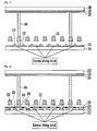
- FIG. 2 is a front view of a field emission back light unit helpful to understand the present invention
- FIG. 3 illustrates UV backside exposure
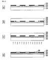
- FIG. 4 illustrates a process of fabricating a cathode structure for a field emission back light unit by backside exposure helpful to understand the present invention
- FIG. 5 is a plan view of a field emission back light unit helpful to understand the present invention.
- FIG. 6 illustrates a local dimming state exhibited by the field emission back light unit
- FIG. 7 illustrates the location of the spacers according to an exemplary embodiment of the present invention.
- a conventional field emission back light unit capable of local dimming used as a back light for a liquid crystal display partially controls brightness by changing current flowing into each of cathode electrodes formed on a cathode substrate, and for precise local dimming, the cathode electrode has to be made small and increased in number.
- the number of interconnections to be connected with an external driver is also increased, and the interconnections are very difficult to be connected with the external driver within a limited space.
- the present invention provides a device which is not limited to the number of unit blocks capable of local dimming and easily connects the external driver with an electrode.
- FIG. 2 illustrates a field emission back light unit helpful to understand the present invention.
- a field emission back light unit includes a lower substrate 210 as a cathode substrate, a plurality of data electrodes 212 formed on the lower substrate 210, an insulating layer 214 formed on the data electrode 212, a cathode electrode 216 formed on the insulating layer 214, a field emitter 218 formed on the cathode electrode 216, an upper substrate 220 as an anode substrate, an anode electrode 222 formed on the upper substrate 220, a phosphor layer 224 formed on the anode electrode 222, a metal gate substrate 232, and spacers 242 and 244.
- the lower substrate 210 is spaced apart from and faces the upper substrate 220, and maintains a specific distance therebetween by the spacer 242 formed between the lower substrate 210 and the metal gate substrate 232, and the spacer 244 formed between the upper substrate 220 and the metal gate substrate 232.
- the lower substrate 210 and the upper substrate 220 may be glass substrates.
- the plurality of data electrodes 212 are formed on the lower substrate 210, and spaced a specific distance apart from one another.
- the data electrode 212 may be formed of a transparent conductive material, which may be indium tin oxide (ITO), indium zinc oxide (IZO), indium tin zinc oxide (ITZO) or carbon nano tube (CNT).
- ITO indium tin oxide
- IZO indium zinc oxide
- ITZO indium tin zinc oxide
- CNT carbon nano tube
- the data electrode 212 is formed of a transparent conductive material to facilitate backside exposure using UV when forming the field emitter.
- an opaque electrode can be used as the data electrode.
- the insulating layer 214 is formed on the data electrode 212, and includes exposure regions 215 exposing predetermined data electrodes 212.
- the cathode electrodes 216 are formed on the insulating layer 214, and electrically connected with the data electrodes 212 through the exposure regions 215.
- a cathode block 211 is defined based on the cathode electrodes 216 electrically isolated from each other, and brightness of the cathode block 211 can be controlled according to current supplied through the data electrode 212.
- the cathode electrode 216 may be formed of a conductive material capable of blocking light. This is to facilitate the backside exposure using UV when forming the field emitter.
- At least one field emitter 218 is formed on the cathode electrode 216, and preferably, a plurality of field emitters 218 are formed to be spaced a specific distance apart from one another.
- the field emitter 218 may be formed of an electron emission material having an excellent electron emission characteristic, which includes carbon nano tube, carbon nano fiber and a carbonaceous synthetic material.
- the anode electrode 222 is formed on the upper substrate 220, and the phosphor layer 224 is coated on the anode electrode 222.
- the anode electrode 222 may also be formed of a transparent conductive material, such as ITO, IZO or ITZO.
- the metal gate substrate 232 serves as a gate electrode inducing electron emission from the field emitter 218, and spaced a specific distance apart from the upper and lower substrates 220 and 210 by the spacers 242 and 244.
- a plurality of openings 236 are formed in the metal gate substrate 232, wherein the opening 236 may be formed to correspond to a location of the field emitter 218.
- the field emission back light unit capable of local dimming controls the brightness of each of the cathode block 211 according to the change of current flowing through the data electrode 212. That is, one of the data electrodes 212 included in each cathode block 211 is used as an electrode interconnection for one cathode block thereby facilitating connection of the electrode with an external driver.
- the data electrode 212 and the insulating layer 214 of the field emission back light unit may be formed of a transparent material, and the cathode electrode 216 may be formed of a conductive material capable of blocking light. These are to facilitate the UV backside exposure when the field emitter is formed of an exposure paste using a carbonaceous material.
- a method of fabricating a field emitter by UV backside exposure will be described with reference to FIG. 3 .
- the method does not fall under the scope of the claims, but represents background art provided for better understanding the present invention.
- a data electrode 312 aud an insulating layer 314 are formed on a transparent substrate 310, and a pattern 316 for forming a field emitter is formed on the insulating layer 314.
- the data electrode 312 and the insulating layer 314 are formed of a transparent material, and the pattern 316 for forming the field emitter is formed of an opaque conductive material.
- a carbonaceous material-negative exposure paste 318 is printed on the stacked structure by screen printing.
- FIG. 3(d) a structure as in FIG. 3(d) is formed by drying the structure, irradiating UV light on a bottom surface of the substrate 310, and developing the structure as illustrated in FIG. 3(c) .
- the exposure paste 318 is removed from a UV-blocked region by a pattern, and post-processes such as annealing and surface treatments are performed, thereby finally completing the field emitter 320. While most of the area of the field emitter formed as such is in contact with the insulating layer, an edge of the field emitter is in contact with a cathode electrode, and thus current required for field emission can be supplied to the emitter.
- the field emitters are labeled to a uniform height, so that the field emitter having a uniform height and high reliability can be formed.
- FIG. 4 illustrates a process of fabricating a cathode substrate for a field emission back light unit using backside exposure helpful to understand the present invention.
- a data electrode 212 having a pattern is formed on a transparent substrate 210.
- the data electrode 212 is formed of a transparent material.
- an insulating layer 214 is formed on the data electrode 212.
- the insulating layer 214 is formed of a transparent material, and has exposure regions 215 exposing the predetermined data electrodes 212 to form a cathode block 211.
- a cathode electrode 216 is formed on the insulating layer 214.
- the cathode electrode 216 is formed, considering a size and a distance of the cathode block 211. That is, it is preferable that a sufficient distance for electrical insulation between the cathode blocks 211 is maintained, and an interface between the blocks not be exposed during emission of a phosphor.
- an emitter paste 218 is applied to the structure except an isolation region 217 for electrically isolating the cathode blocks 211.
- a cathode substrate is completed, in which the cathode blocks 211 are electrically isolated from one another as in FIG. 4(f) .
- the data and cathode electrodes, and the insulating layer may be easily formed by conventional deposition, and photolithography or screen printing.
- FIG. 5 illustrates the cathode substrate completed by the above-described process.
- an exposure region 215 is formed on each cathode block 211, and as described above, the cathode electrodes 216 correspond to and are electrically connected with the data electrodes 212 one by one through the exposure regions 215.
- the current flows into only one cathode electrode 216, and thus the brightness can be controlled by cathode blocks 211 in the cathode substrate formed as such.
- an interconnection between the cathode block 211 and an electrode is formed very simply by the data electrode 212 and the insulating layer 214.
- FIG. 6 illustrates a local dimming state exhibited by the field emission back light unit described above.
- voltage applied to a metal gate substrate and an anode electrode is fixed, and an amount of current flowing through a cathode electrode and a data electrode, which are electrically connected with a specific field emitter, is controlled, thereby controlling an amount of electron beam emitted from the field emitter, so that a gray scale of a specific part can be expressed.
- the amount of current may be controlled by a semiconductor switching circuit such as a TFT or a MOSFET, and an amount of electrons flowing into the emitter may be controlled from the cathode electrode, which is isolated in pulse width modulation (PWM) or pulse amplitude modulation (PAM).
- PWM pulse width modulation
- PAM pulse amplitude modulation
- FIG. 7 illustrates an exemplary embodiment of the invention. Since the spacers 242 are formed at the locations of the exposure regions 214 where the field emitter 218 is not formed, the non-emission region of the field emission back light unit can be minimized.
- interconnections connected with an external electrode may be simply formed by a dual structure of a data electrode and an insulating layer.
Landscapes
- Physics & Mathematics (AREA)
- Nonlinear Science (AREA)
- Mathematical Physics (AREA)
- Chemical & Material Sciences (AREA)
- Crystallography & Structural Chemistry (AREA)
- General Physics & Mathematics (AREA)
- Optics & Photonics (AREA)
- Cold Cathode And The Manufacture (AREA)
- Discharge Lamps And Accessories Thereof (AREA)
Description
- The present invention relates to a field emission back light unit which is capable of local dimming and a method of fabricating the same.
- Generally, flat panel displays may be classified into emissive displays and non-emissive displays.
- The emissive displays include a plasma display panel (PDP) display and a field emission display (FED), and the non-emissive displays include a liquid crystal display (LCD).
- While the LCD, a non-emissive display, has light weight and low power consumption, it cannot create an image by self-emission, but only by light entering from outside. Thus, the image created by the LCD cannot be observed in a dark place. To solve this problem, a back light unit is equipped at a back surface of the LCD.
- Conventionally, as a back light unit, a cold cathode fluorescent lamp (CCFL), which is a linear light source, and a light emitting diode (LED), which is a spot light source, are mainly used.
- However, such back light units are complicated and expensive, and consume a large amount of power according to reflection and transmission of light due to the light source disposed at a side thereof. Particularly, as the LCD becomes larger, uniform brightness becomes difficult to ensure.
- For these reasons, in recent time, a field emission back light unit having a flat emission structure has been developed. Such a field emission back light unit consumes less power and exhibits relatively uniform brightness in a wide range of an emission region, compared to the conventional back light unit using a CCFL.
- Generally, in a field emission-back light unit, a cathode substrate having a field emitter and an anode substrate having a phosphor are disposed to face and be spaced a specific distance apart from each other, and vacuum-packed. An electron emitted from the field emitter collides with the phosphor of the anode substrate, so that light is emitted by cathodoluminescence of the phosphor.
- A structure of the conventional field emission back light unit will now be described with reference to
FIG. 1 . -
FIG. 1 illustrates the field emission back light unit capable of local dimming, which has a metal gate substrate. - Referring to
FIG. 1 , the conventional field emission back light unit having the metal gate substrate includes a cathode substrate as alower substrate 110, a plurality ofcathode electrodes 112 formed on thelower substrate 110, afield emitter 114 formed on the plurality ofcathode electrodes 112, an anode substrate as anupper substrate 120, an anode electrode 122 formed on theupper substrate 120, aphosphor layer 124 formed on the anode electrode 122, ametal gate substrate 132 andspacers - When a specific amount of current is applied to the
cathode electrode 112, thefield emitter 114 emits an electron beam, which is radially propagated. As a result, the electron beam emitted from thefield emitter 114 reaches aphosphor 124 corresponding to a pixel, and thephosphor 124 emits light. - Meanwhile, for partial control of brightness and a high contrast ratio, an amount of current applied to the plurality of
cathode electrodes 112 is controlled. For precise local dimming, the number ofcathode electrodes 112 has to be increased, which makes interconnections connected with an external electrode complicated. - Thus, a method for effectively performing local dimming without complicated interconnections connected with an external electrode is needed.
-
WO 20071058502 A1 -
US 2006/0231837 A1 relates to a thin-film assembly. The thin-film assembly includes a substrate and at least one electronic thin-film component applied on the substrate by thin-film technology, wherein a base electrode is provided on the substrate, on which base electrode thin-film layers forming part of the thin-film component are arranged together with an upper top electrode. The substrate is comprised of a printed circuit board and includes an insulating material base body and a metal coating as the conductor layer, wherein the conductor layer forms the base electrode and is smoothed at least on the location of the thin-film component. It is furthermore disclosed that a contact layer is applied by thin-film technology between the smoothed conductor layer and the superimposed thin-film layers of the thin-film component, wherein the contact layer is physically or chemically absorbed on the surface of the base electrode. - The present invention is directed to a field emission back light unit having simple interconnections connected with an external electrode and capable of local dimming.
- Other objects of the present invention will be understood with reference to following descriptions and exemplary embodiments of the present invention.
- The present invention is defined in the appended
independent claim 1. The appended dependent claims 2-7 define preferred embodiments. - A cathode structure for a field emission back light unit includes: a plurality of data electrodes formed on a cathode substrate and spaced apart from one another; an insulating layer formed on the data electrodes, and having exposure regions exposing the predetermined data electrodes; cathode electrodes formed on the insulating layer and electrically connected with the data electrodes through the exposure regions; and at least one field emitter formed on the cathode electrode, wherein a cathode block is defined based on the cathode electrodes electrically isolated from one another, and brightness of each cathode block can be controlled according to current supplied through the data electrode.
- A method of fabricating a cathode structure for the field emission back light unit includes: defining cathode blocks for controlling brightness by blocks on a transparent substrate; forming a plurality of data electrodes spaced apart from one another on the respective cathode blocks; forming an insulating layer having an exposure region exposing any one of the data electrodes formed on the respective cathode blocks; forming a plurality of cathode electrodes spaced apart from one another on the insulating layer, any one of the cathode electrodes being electrically connected with the data electrode through the exposure region; applying an emitter paste to the cathode electrode except a part of the insulating layer, in which the cathode electrode is not formed; and irradiating UV light on a bottom surface of the substrate and developing the substrate.
- A field emission back light unit includes: an upper substrate and a lower substrate, which are spaced apart from and face each other; an anode electrode and a phosphor layer, which are formed on the upper substrate; a metal gate substrate disposed between the upper and lower substrates to induce electron emission from a field emitter, and having an opening to pass the emitted electron therethrough; a plurality of data electrodes spaced apart from one another on the lower substrate; an insulating layer formed on the data electrodes and having exposure regions exposing the predetermined data electrodes; cathode electrodes formed on the insulating layer and electrically connected with the data electrodes through the exposure regions; and at least one field emitter formed on the cathode electrode, wherein a cathode block is defined based on the cathode electrodes electrically isolated from one another, and brightness of the cathode block can be controlled according to current supplied through the data electrode.
- As described above, interconnections connected with an external electrode may be simply formed by a dual structure of a data electrode and an insulating layer.
-
FIG. 1 illustrates a field emission back light unit capable of local dimming, which has a metal gate substrate; -
FIG. 2 is a front view of a field emission back light unit helpful to understand the present invention; -
FIG. 3 illustrates UV backside exposure; -
FIG. 4 illustrates a process of fabricating a cathode structure for a field emission back light unit by backside exposure helpful to understand the present invention; -
FIG. 5 is a plan view of a field emission back light unit helpful to understand the present invention; -
FIG. 6 illustrates a local dimming state exhibited by the field emission back light unit and -
FIG. 7 illustrates the location of the spacers according to an exemplary embodiment of the present invention. - In the following description, it is to be noted that a detailed description of the known function and configuration of the present invention will be omitted if it is deemed to obscure the subject matter of the present invention. The terms described below, as terms defined considering their functions in the present invention, can be different depending on a user or operator's intention, or a practice. Thus, the definition should be made on the basis of the contents throughout this specification.
- A conventional field emission back light unit capable of local dimming used as a back light for a liquid crystal display partially controls brightness by changing current flowing into each of cathode electrodes formed on a cathode substrate, and for precise local dimming, the cathode electrode has to be made small and increased in number. However, as described above, according to the increased number of cathode electrodes, the number of interconnections to be connected with an external driver is also increased, and the interconnections are very difficult to be connected with the external driver within a limited space. To solve this problem, the present invention provides a device which is not limited to the number of unit blocks capable of local dimming and easily connects the external driver with an electrode.
- Examples helpful to understand the present invention and an exemplary embodiment of the present invention will now be described with reference to accompanying drawings in detail.
-
FIG. 2 illustrates a field emission back light unit helpful to understand the present invention. - Referring to
FIG. 2 , a field emission back light unit includes alower substrate 210 as a cathode substrate, a plurality ofdata electrodes 212 formed on thelower substrate 210, aninsulating layer 214 formed on thedata electrode 212, acathode electrode 216 formed on theinsulating layer 214, afield emitter 218 formed on thecathode electrode 216, an upper substrate 220 as an anode substrate, ananode electrode 222 formed on the upper substrate 220, a phosphor layer 224 formed on theanode electrode 222, ametal gate substrate 232, andspacers - The
lower substrate 210 is spaced apart from and faces the upper substrate 220, and maintains a specific distance therebetween by thespacer 242 formed between thelower substrate 210 and themetal gate substrate 232, and thespacer 244 formed between the upper substrate 220 and themetal gate substrate 232. Thelower substrate 210 and the upper substrate 220 may be glass substrates. - The plurality of
data electrodes 212 are formed on thelower substrate 210, and spaced a specific distance apart from one another. Thedata electrode 212 may be formed of a transparent conductive material, which may be indium tin oxide (ITO), indium zinc oxide (IZO), indium tin zinc oxide (ITZO) or carbon nano tube (CNT). Here, thedata electrode 212 is formed of a transparent conductive material to facilitate backside exposure using UV when forming the field emitter. However, when an opening the same as that in the cathode electrode, in which the field emitter is formed in the opening of the cathode electrode, is formed in the data electrode, an opaque electrode can be used as the data electrode. - The
insulating layer 214 is formed on thedata electrode 212, and includesexposure regions 215 exposingpredetermined data electrodes 212. - The
cathode electrodes 216 are formed on the insulatinglayer 214, and electrically connected with thedata electrodes 212 through theexposure regions 215. - Meanwhile, among the
cathode electrodes 216, acathode block 211 is defined based on thecathode electrodes 216 electrically isolated from each other, and brightness of thecathode block 211 can be controlled according to current supplied through thedata electrode 212. - The
cathode electrode 216 may be formed of a conductive material capable of blocking light. This is to facilitate the backside exposure using UV when forming the field emitter. - At least one
field emitter 218 is formed on thecathode electrode 216, and preferably, a plurality offield emitters 218 are formed to be spaced a specific distance apart from one another. - The
field emitter 218 may be formed of an electron emission material having an excellent electron emission characteristic, which includes carbon nano tube, carbon nano fiber and a carbonaceous synthetic material. - The
anode electrode 222 is formed on the upper substrate 220, and the phosphor layer 224 is coated on theanode electrode 222. Theanode electrode 222 may also be formed of a transparent conductive material, such as ITO, IZO or ITZO. - The
metal gate substrate 232 serves as a gate electrode inducing electron emission from thefield emitter 218, and spaced a specific distance apart from the upper andlower substrates 220 and 210 by thespacers - A plurality of
openings 236 are formed in themetal gate substrate 232, wherein theopening 236 may be formed to correspond to a location of thefield emitter 218. - The field emission back light unit capable of local dimming having the above-described structure controls the brightness of each of the
cathode block 211 according to the change of current flowing through thedata electrode 212. That is, one of thedata electrodes 212 included in eachcathode block 211 is used as an electrode interconnection for one cathode block thereby facilitating connection of the electrode with an external driver. - As described above, the
data electrode 212 and the insulatinglayer 214 of the field emission back light unit may be formed of a transparent material, and thecathode electrode 216 may be formed of a conductive material capable of blocking light. These are to facilitate the UV backside exposure when the field emitter is formed of an exposure paste using a carbonaceous material. - A method of fabricating a field emitter by UV backside exposure will be described with reference to
FIG. 3 . The method does not fall under the scope of the claims, but represents background art provided for better understanding the present invention. - First, as in
FIG. 3(a) , a data electrode 312 aud an insulating layer 314 are formed on atransparent substrate 310, and a pattern 316 for forming a field emitter is formed on the insulating layer 314. - Here, the data electrode 312 and the insulating layer 314 are formed of a transparent material, and the pattern 316 for forming the field emitter is formed of an opaque conductive material.
- Subsequently, as in
FIG. 3(b) , a carbonaceous material-negative exposure paste 318 is printed on the stacked structure by screen printing. - Then, a structure as in
FIG. 3(d) is formed by drying the structure, irradiating UV light on a bottom surface of thesubstrate 310, and developing the structure as illustrated inFIG. 3(c) . - That is, the exposure paste 318 is removed from a UV-blocked region by a pattern, and post-processes such as annealing and surface treatments are performed, thereby finally completing the
field emitter 320. While most of the area of the field emitter formed as such is in contact with the insulating layer, an edge of the field emitter is in contact with a cathode electrode, and thus current required for field emission can be supplied to the emitter. When the field emitter is formed using the backside exposure, the field emitters are labeled to a uniform height, so that the field emitter having a uniform height and high reliability can be formed. -
FIG. 4 illustrates a process of fabricating a cathode substrate for a field emission back light unit using backside exposure helpful to understand the present invention. - First, as in
FIG. 4(a) , adata electrode 212 having a pattern is formed on atransparent substrate 210. Here, thedata electrode 212 is formed of a transparent material. - After that, as in
FIG. 4(b) , an insulatinglayer 214 is formed on thedata electrode 212. Here, the insulatinglayer 214 is formed of a transparent material, and hasexposure regions 215 exposing thepredetermined data electrodes 212 to form acathode block 211. - Then, as in
FIG. 4(c) , acathode electrode 216 is formed on the insulatinglayer 214. Here, thecathode electrode 216 is formed, considering a size and a distance of thecathode block 211. That is, it is preferable that a sufficient distance for electrical insulation between the cathode blocks 211 is maintained, and an interface between the blocks not be exposed during emission of a phosphor. - As in
FIG. 4(d) , anemitter paste 218 is applied to the structure except anisolation region 217 for electrically isolating the cathode blocks 211. - After the backside exposure by irradiating UV light on a bottom surface of the substrate and development as in
FIG. 4(e) , a cathode substrate is completed, in which the cathode blocks 211 are electrically isolated from one another as inFIG. 4(f) . - The data and cathode electrodes, and the insulating layer may be easily formed by conventional deposition, and photolithography or screen printing.
-
FIG. 5 illustrates the cathode substrate completed by the above-described process. - Referring to
FIG. 5 , it can be seen that anexposure region 215 is formed on eachcathode block 211, and as described above, thecathode electrodes 216 correspond to and are electrically connected with thedata electrodes 212 one by one through theexposure regions 215. When current is applied to any one of thedata electrodes 212, the current flows into only onecathode electrode 216, and thus the brightness can be controlled bycathode blocks 211 in the cathode substrate formed as such. Further, it can be seen that an interconnection between thecathode block 211 and an electrode is formed very simply by thedata electrode 212 and the insulatinglayer 214. -
FIG. 6 illustrates a local dimming state exhibited by the field emission back light unit described above. During the local dimming, voltage applied to a metal gate substrate and an anode electrode is fixed, and an amount of current flowing through a cathode electrode and a data electrode, which are electrically connected with a specific field emitter, is controlled, thereby controlling an amount of electron beam emitted from the field emitter, so that a gray scale of a specific part can be expressed. - Here, the amount of current may be controlled by a semiconductor switching circuit such as a TFT or a MOSFET, and an amount of electrons flowing into the emitter may be controlled from the cathode electrode, which is isolated in pulse width modulation (PWM) or pulse amplitude modulation (PAM).
- Meanwhile,
FIG. 7 illustrates an exemplary embodiment of the invention. Since thespacers 242 are formed at the locations of theexposure regions 214 where thefield emitter 218 is not formed, the non-emission region of the field emission back light unit can be minimized. - As described above, interconnections connected with an external electrode may be simply formed by a dual structure of a data electrode and an insulating layer.
- While the invention has been shown and described with reference to certain exemplary embodiments thereof, it will be understood by those skilled in the art that various changes in form and details may be made therein without departing from the scope of the invention as defined by the appended claims.
Claims (7)
- A field emission back light unit, comprising:an upper substrate (220) and a lower substrate (210), which are spaced apart from and face each other;an anode electrode (222) and a phosphor layer (224), which are formed on the upper substrate (220);a metal gate substrate (232) disposed between the upper and lower substrates to induce electron emission from field emitters (218) on the lower substrate (210), and having an opening (236) to pass the emitted electron therethrough;a plurality of data electrodes (212) spaced apart from one another on the lower substrate (210);an insulating layer (214) formed on the data electrodes (212) and having exposure regions (215) exposing the predetermined data electrodes (212);cathode electrodes (216) formed on the insulating layer (214) and each electrically connected with a respective data electrode (212) through a respective exposure region (215);at least one of said field emitters (218) formed on each cathodes electrode (216); andinsulating spacers (242, 244) formed on the exposure regions (215), between the lower substrate (210) and the metal gate substrate (232), and the upper substrate (220) and the metal gate substrate (232), respectively,wherein said cathode electrodes (216) are electrically isolated from one another and each form a cathode block (211) which is adapted to control electron emission of the field emitter (218) or field emitters (218) formed thereon according to current supplied through the corresponding data electrode (212).
- The field emission back light unit according to claim 1, wherein the data electrodes (212) are formed of a transparent conductive material.
- The field emission back light unit according to claim 2, wherein the transparent conductive material is any one of the ITO, IZO, ITZO and CNT.
- The field emission back light unit according to claim 1, wherein an isolation region (217) in which the cathode electrodes (216) are not formed on the insulating layer (214) is formed to electrically isolate the adjacent cathode blocks (211) from one another.
- The field emission back light unit according to claim 1, wherein the cathode electrodes (216) are formed of a conductive material capable of blocking light.
- The field emission back light unit according to claim 1, wherein each field emitter (218) is formed of any one of carbon nano tube, carbon nano fiber and a carbonaceous synthetic material.
- A method of fabricating a field emission back light unit according to any one of claims 1 to 6, comprising:forming a plurality of data electrodes (212) spaced apart from one another on a top surface of a transparent substrate (210);forming an insulating layer (214) on the data electrodes (212) and forming exposure regions (215) in the insulating layer (214) exposing the predetermined data electrodes (212);forming a plurality of cathode electrodes (216) spaced apart from one another on the insulating layer (214), any one of the cathode electrodes (216) being electrically connected with a respective data electrode (212) through a respective exposure region (215);applying an emitter paste on the cathode electrodes (216) except an electric isolation region (217) between the cathode electrodes (216);irradiating UV light on the bottom surface of the transparent substrate (210) and developing the formed structure to obtain the at least one field emitter (218) on each cathode (216) andforming insulating spacers (242, 244) on the exposure regions (215).
Applications Claiming Priority (2)
| Application Number | Priority Date | Filing Date | Title |
|---|---|---|---|
| KR1020070132746A KR100913132B1 (en) | 2007-12-17 | 2007-12-17 | Field emission type backlight unit, cathode structure and method of manufacturing same |
| PCT/KR2008/003634 WO2009078518A1 (en) | 2007-12-17 | 2008-06-25 | Field emission back light unit, cathode structure thereof and method for fabricating the same |
Publications (3)
| Publication Number | Publication Date |
|---|---|
| EP2225606A1 EP2225606A1 (en) | 2010-09-08 |
| EP2225606A4 EP2225606A4 (en) | 2011-02-23 |
| EP2225606B1 true EP2225606B1 (en) | 2013-03-27 |
Family
ID=40795625
Family Applications (1)
| Application Number | Title | Priority Date | Filing Date |
|---|---|---|---|
| EP08766593A Not-in-force EP2225606B1 (en) | 2007-12-17 | 2008-06-25 | Field emission back light unit and method for fabricating the same |
Country Status (6)
| Country | Link |
|---|---|
| US (1) | US8093795B2 (en) |
| EP (1) | EP2225606B1 (en) |
| JP (1) | JP5319695B2 (en) |
| KR (1) | KR100913132B1 (en) |
| CN (1) | CN101868753B (en) |
| WO (1) | WO2009078518A1 (en) |
Families Citing this family (6)
| Publication number | Priority date | Publication date | Assignee | Title |
|---|---|---|---|---|
| KR101343567B1 (en) * | 2009-12-21 | 2013-12-20 | 한국전자통신연구원 | field emission device |
| JP5307766B2 (en) * | 2009-12-21 | 2013-10-02 | 韓國電子通信研究院 | Field emission device |
| TWI434320B (en) * | 2011-12-08 | 2014-04-11 | Au Optronics Corp | Field emission backlight module, display, and bowl-shaped reflective structure manufacturing method |
| JPWO2016111125A1 (en) * | 2015-01-08 | 2017-10-12 | リンテック株式会社 | Thermoelectric converter and power storage system |
| CN107504402B (en) * | 2017-08-30 | 2019-11-22 | 厦门天马微电子有限公司 | Back light and display device |
| CN109116631B (en) * | 2018-09-30 | 2021-06-15 | 厦门天马微电子有限公司 | Backlight module, liquid crystal display module and electronic equipment |
Family Cites Families (17)
| Publication number | Priority date | Publication date | Assignee | Title |
|---|---|---|---|---|
| JPH0621150U (en) * | 1992-04-28 | 1994-03-18 | 双葉電子工業株式会社 | Fluorescent tube |
| JP2000323078A (en) * | 1999-05-14 | 2000-11-24 | Ise Electronics Corp | Fluorescent display device |
| JP2001035352A (en) * | 1999-07-22 | 2001-02-09 | Sharp Corp | Electron source, method of manufacturing the same, and image forming apparatus formed using the same |
| JP2001222967A (en) * | 2000-02-07 | 2001-08-17 | Sony Corp | Field emission display device and method of manufacturing the same |
| US6441559B1 (en) | 2000-04-28 | 2002-08-27 | Motorola, Inc. | Field emission display having an invisible spacer and method |
| EP1221710B1 (en) * | 2001-01-05 | 2004-10-27 | Samsung SDI Co. Ltd. | Method of manufacturing triode carbon nanotube field emitter array |
| JP2003217478A (en) | 2002-01-24 | 2003-07-31 | Asahi Glass Co Ltd | Field emission display device |
| US6929042B2 (en) * | 2003-07-30 | 2005-08-16 | Chi-Lo Chang | Semi-automatic mortising machine |
| AT500259B1 (en) * | 2003-09-09 | 2007-08-15 | Austria Tech & System Tech | THIN-LAYER ASSEMBLY AND METHOD FOR PRODUCING SUCH A THIN-LAYER ASSEMBLY |
| TWI231521B (en) * | 2003-09-25 | 2005-04-21 | Ind Tech Res Inst | A carbon nanotubes field emission display and the fabricating method of which |
| KR20050041726A (en) | 2003-10-31 | 2005-05-04 | 삼성에스디아이 주식회사 | Field emission display device and manufacturing method of the same |
| KR20050062742A (en) * | 2003-12-22 | 2005-06-27 | 삼성에스디아이 주식회사 | Field emission device, display adopting the same and and method of manufacturing the same |
| JP2005310489A (en) * | 2004-04-20 | 2005-11-04 | Toshiba Corp | Display device |
| KR20050110189A (en) * | 2004-05-18 | 2005-11-23 | 삼성에스디아이 주식회사 | Electron emission device |
| WO2007007472A1 (en) * | 2005-07-07 | 2007-01-18 | Sharp Kabushiki Kaisha | Display unit |
| KR100732845B1 (en) * | 2005-11-17 | 2007-06-27 | 이승호 | Planar light emitting device for TFT-LCD using carbon nanotube |
| KR100963258B1 (en) | 2007-09-07 | 2010-06-11 | 한국전자통신연구원 | Field emission device |
-
2007
- 2007-12-17 KR KR1020070132746A patent/KR100913132B1/en not_active Expired - Fee Related
-
2008
- 2008-06-25 EP EP08766593A patent/EP2225606B1/en not_active Not-in-force
- 2008-06-25 US US12/739,190 patent/US8093795B2/en active Active
- 2008-06-25 JP JP2010536832A patent/JP5319695B2/en not_active Expired - Fee Related
- 2008-06-25 WO PCT/KR2008/003634 patent/WO2009078518A1/en not_active Ceased
- 2008-06-25 CN CN2008801164694A patent/CN101868753B/en not_active Expired - Fee Related
Also Published As
| Publication number | Publication date |
|---|---|
| US8093795B2 (en) | 2012-01-10 |
| KR100913132B1 (en) | 2009-08-19 |
| EP2225606A1 (en) | 2010-09-08 |
| JP2011507155A (en) | 2011-03-03 |
| EP2225606A4 (en) | 2011-02-23 |
| WO2009078518A1 (en) | 2009-06-25 |
| JP5319695B2 (en) | 2013-10-16 |
| US20100225225A1 (en) | 2010-09-09 |
| CN101868753B (en) | 2013-07-10 |
| KR20090065265A (en) | 2009-06-22 |
| CN101868753A (en) | 2010-10-20 |
Similar Documents
| Publication | Publication Date | Title |
|---|---|---|
| KR100697656B1 (en) | Planar Light Emitting Device with Multiple Electron Sources | |
| CN103323975B (en) | A kind of array base palte, display panels and display device | |
| CN101372618A (en) | White phosphor, light emitting device including the same, and display | |
| US8093795B2 (en) | Field emission back light unit, cathode structure thereof and method for fabricating the same | |
| US20020079826A1 (en) | Flat luminescence lamp and method for manufacturing the same | |
| CN100401525C (en) | Organic electroluminescence display device and manufacturing method thereof | |
| CN102800815B (en) | Display device and manufacturing method thereof | |
| TWI271766B (en) | Composite substrate able to emit light from both sides | |
| JP4326542B2 (en) | Surface light source device and liquid crystal display device using the same | |
| KR100785030B1 (en) | Field emission device and manufacturing method thereof | |
| KR20070013873A (en) | Electromagnetic Emission Backlight Unit and Flat Panel Display | |
| US8129895B2 (en) | Field emission device with fine local dimming | |
| KR100705270B1 (en) | Organic electroluminescent display and manufacturing method | |
| KR100625033B1 (en) | Organic electroluminescent display device and manufacturing method thereof | |
| CN100395865C (en) | Composite substrate capable of emitting light from both sides | |
| KR100625032B1 (en) | Organic electroluminescent display device and manufacturing method thereof | |
| KR20060084501A (en) | Field emission device using electromagnetic field and driving method thereof | |
| KR20070099268A (en) | Field emission type backlight unit and manufacturing method thereof | |
| KR100556697B1 (en) | Organic electroluminescent device and manufacturing method thereof | |
| KR101352313B1 (en) | Light Emitting Panel | |
| KR100846708B1 (en) | Light emitting device and display device | |
| KR20080061547A (en) | Flat panel and its manufacturing method | |
| KR20060102088A (en) | Organic electroluminescent display device, manufacturing method thereof and repair method using same | |
| KR20080080845A (en) | EL panel | |
| KR20010004757A (en) | Dual layer vacuum fluorescent display |
Legal Events
| Date | Code | Title | Description |
|---|---|---|---|
| PUAI | Public reference made under article 153(3) epc to a published international application that has entered the european phase |
Free format text: ORIGINAL CODE: 0009012 |
|
| 17P | Request for examination filed |
Effective date: 20100719 |
|
| AK | Designated contracting states |
Kind code of ref document: A1 Designated state(s): AT BE BG CH CY CZ DE DK EE ES FI FR GB GR HR HU IE IS IT LI LT LU LV MC MT NL NO PL PT RO SE SI SK TR |
|
| AX | Request for extension of the european patent |
Extension state: AL BA MK RS |
|
| A4 | Supplementary search report drawn up and despatched |
Effective date: 20110120 |
|
| RIC1 | Information provided on ipc code assigned before grant |
Ipc: H01J 1/304 20060101ALI20110114BHEP Ipc: G02F 1/13357 20060101AFI20090708BHEP |
|
| DAX | Request for extension of the european patent (deleted) | ||
| 17Q | First examination report despatched |
Effective date: 20110919 |
|
| GRAP | Despatch of communication of intention to grant a patent |
Free format text: ORIGINAL CODE: EPIDOSNIGR1 |
|
| GRAC | Information related to communication of intention to grant a patent modified |
Free format text: ORIGINAL CODE: EPIDOSCIGR1 |
|
| RIC1 | Information provided on ipc code assigned before grant |
Ipc: H01J 63/02 20060101ALI20120112BHEP Ipc: H01J 1/304 20060101ALI20120112BHEP Ipc: G02F 1/13357 20060101AFI20120112BHEP |
|
| RTI1 | Title (correction) |
Free format text: FIELD EMISSION BACK LIGHT UNIT AND METHOD FOR FABRICATING THE SAME |
|
| RIN1 | Information on inventor provided before grant (corrected) |
Inventor name: JEONG, JIN WOO Inventor name: SONG, YOON HO Inventor name: KIM, DAE JUN |
|
| GRAS | Grant fee paid |
Free format text: ORIGINAL CODE: EPIDOSNIGR3 |
|
| GRAJ | Information related to disapproval of communication of intention to grant by the applicant or resumption of examination proceedings by the epo deleted |
Free format text: ORIGINAL CODE: EPIDOSDIGR1 |
|
| GRAP | Despatch of communication of intention to grant a patent |
Free format text: ORIGINAL CODE: EPIDOSNIGR1 |
|
| GRAS | Grant fee paid |
Free format text: ORIGINAL CODE: EPIDOSNIGR3 |
|
| GRAA | (expected) grant |
Free format text: ORIGINAL CODE: 0009210 |
|
| AK | Designated contracting states |
Kind code of ref document: B1 Designated state(s): AT BE BG CH CY CZ DE DK EE ES FI FR GB GR HR HU IE IS IT LI LT LU LV MC MT NL NO PL PT RO SE SI SK TR |
|
| REG | Reference to a national code |
Ref country code: GB Ref legal event code: FG4D |
|
| REG | Reference to a national code |
Ref country code: CH Ref legal event code: EP |
|
| REG | Reference to a national code |
Ref country code: AT Ref legal event code: REF Ref document number: 603748 Country of ref document: AT Kind code of ref document: T Effective date: 20130415 |
|
| REG | Reference to a national code |
Ref country code: IE Ref legal event code: FG4D |
|
| REG | Reference to a national code |
Ref country code: DE Ref legal event code: R096 Ref document number: 602008023264 Country of ref document: DE Effective date: 20130523 |
|
| PG25 | Lapsed in a contracting state [announced via postgrant information from national office to epo] |
Ref country code: NO Free format text: LAPSE BECAUSE OF FAILURE TO SUBMIT A TRANSLATION OF THE DESCRIPTION OR TO PAY THE FEE WITHIN THE PRESCRIBED TIME-LIMIT Effective date: 20130627 Ref country code: LT Free format text: LAPSE BECAUSE OF FAILURE TO SUBMIT A TRANSLATION OF THE DESCRIPTION OR TO PAY THE FEE WITHIN THE PRESCRIBED TIME-LIMIT Effective date: 20130327 Ref country code: BG Free format text: LAPSE BECAUSE OF FAILURE TO SUBMIT A TRANSLATION OF THE DESCRIPTION OR TO PAY THE FEE WITHIN THE PRESCRIBED TIME-LIMIT Effective date: 20130627 Ref country code: SE Free format text: LAPSE BECAUSE OF FAILURE TO SUBMIT A TRANSLATION OF THE DESCRIPTION OR TO PAY THE FEE WITHIN THE PRESCRIBED TIME-LIMIT Effective date: 20130327 |
|
| REG | Reference to a national code |
Ref country code: AT Ref legal event code: MK05 Ref document number: 603748 Country of ref document: AT Kind code of ref document: T Effective date: 20130327 |
|
| REG | Reference to a national code |
Ref country code: LT Ref legal event code: MG4D |
|
| PG25 | Lapsed in a contracting state [announced via postgrant information from national office to epo] |
Ref country code: LV Free format text: LAPSE BECAUSE OF FAILURE TO SUBMIT A TRANSLATION OF THE DESCRIPTION OR TO PAY THE FEE WITHIN THE PRESCRIBED TIME-LIMIT Effective date: 20130327 Ref country code: GR Free format text: LAPSE BECAUSE OF FAILURE TO SUBMIT A TRANSLATION OF THE DESCRIPTION OR TO PAY THE FEE WITHIN THE PRESCRIBED TIME-LIMIT Effective date: 20130628 Ref country code: SI Free format text: LAPSE BECAUSE OF FAILURE TO SUBMIT A TRANSLATION OF THE DESCRIPTION OR TO PAY THE FEE WITHIN THE PRESCRIBED TIME-LIMIT Effective date: 20130327 Ref country code: FI Free format text: LAPSE BECAUSE OF FAILURE TO SUBMIT A TRANSLATION OF THE DESCRIPTION OR TO PAY THE FEE WITHIN THE PRESCRIBED TIME-LIMIT Effective date: 20130327 |
|
| REG | Reference to a national code |
Ref country code: NL Ref legal event code: VDEP Effective date: 20130327 |
|
| PG25 | Lapsed in a contracting state [announced via postgrant information from national office to epo] |
Ref country code: HR Free format text: LAPSE BECAUSE OF FAILURE TO SUBMIT A TRANSLATION OF THE DESCRIPTION OR TO PAY THE FEE WITHIN THE PRESCRIBED TIME-LIMIT Effective date: 20130327 Ref country code: BE Free format text: LAPSE BECAUSE OF FAILURE TO SUBMIT A TRANSLATION OF THE DESCRIPTION OR TO PAY THE FEE WITHIN THE PRESCRIBED TIME-LIMIT Effective date: 20130327 |
|
| PG25 | Lapsed in a contracting state [announced via postgrant information from national office to epo] |
Ref country code: AT Free format text: LAPSE BECAUSE OF FAILURE TO SUBMIT A TRANSLATION OF THE DESCRIPTION OR TO PAY THE FEE WITHIN THE PRESCRIBED TIME-LIMIT Effective date: 20130327 Ref country code: ES Free format text: LAPSE BECAUSE OF FAILURE TO SUBMIT A TRANSLATION OF THE DESCRIPTION OR TO PAY THE FEE WITHIN THE PRESCRIBED TIME-LIMIT Effective date: 20130708 Ref country code: CZ Free format text: LAPSE BECAUSE OF FAILURE TO SUBMIT A TRANSLATION OF THE DESCRIPTION OR TO PAY THE FEE WITHIN THE PRESCRIBED TIME-LIMIT Effective date: 20130327 Ref country code: PT Free format text: LAPSE BECAUSE OF FAILURE TO SUBMIT A TRANSLATION OF THE DESCRIPTION OR TO PAY THE FEE WITHIN THE PRESCRIBED TIME-LIMIT Effective date: 20130729 Ref country code: EE Free format text: LAPSE BECAUSE OF FAILURE TO SUBMIT A TRANSLATION OF THE DESCRIPTION OR TO PAY THE FEE WITHIN THE PRESCRIBED TIME-LIMIT Effective date: 20130327 Ref country code: NL Free format text: LAPSE BECAUSE OF FAILURE TO SUBMIT A TRANSLATION OF THE DESCRIPTION OR TO PAY THE FEE WITHIN THE PRESCRIBED TIME-LIMIT Effective date: 20130327 Ref country code: IS Free format text: LAPSE BECAUSE OF FAILURE TO SUBMIT A TRANSLATION OF THE DESCRIPTION OR TO PAY THE FEE WITHIN THE PRESCRIBED TIME-LIMIT Effective date: 20130727 Ref country code: RO Free format text: LAPSE BECAUSE OF FAILURE TO SUBMIT A TRANSLATION OF THE DESCRIPTION OR TO PAY THE FEE WITHIN THE PRESCRIBED TIME-LIMIT Effective date: 20130327 Ref country code: SK Free format text: LAPSE BECAUSE OF FAILURE TO SUBMIT A TRANSLATION OF THE DESCRIPTION OR TO PAY THE FEE WITHIN THE PRESCRIBED TIME-LIMIT Effective date: 20130327 |
|
| PG25 | Lapsed in a contracting state [announced via postgrant information from national office to epo] |
Ref country code: CY Free format text: LAPSE BECAUSE OF FAILURE TO SUBMIT A TRANSLATION OF THE DESCRIPTION OR TO PAY THE FEE WITHIN THE PRESCRIBED TIME-LIMIT Effective date: 20130327 Ref country code: PL Free format text: LAPSE BECAUSE OF FAILURE TO SUBMIT A TRANSLATION OF THE DESCRIPTION OR TO PAY THE FEE WITHIN THE PRESCRIBED TIME-LIMIT Effective date: 20130327 |
|
| PG25 | Lapsed in a contracting state [announced via postgrant information from national office to epo] |
Ref country code: DK Free format text: LAPSE BECAUSE OF FAILURE TO SUBMIT A TRANSLATION OF THE DESCRIPTION OR TO PAY THE FEE WITHIN THE PRESCRIBED TIME-LIMIT Effective date: 20130327 Ref country code: MC Free format text: LAPSE BECAUSE OF FAILURE TO SUBMIT A TRANSLATION OF THE DESCRIPTION OR TO PAY THE FEE WITHIN THE PRESCRIBED TIME-LIMIT Effective date: 20130327 |
|
| PLBE | No opposition filed within time limit |
Free format text: ORIGINAL CODE: 0009261 |
|
| REG | Reference to a national code |
Ref country code: CH Ref legal event code: PL |
|
| STAA | Information on the status of an ep patent application or granted ep patent |
Free format text: STATUS: NO OPPOSITION FILED WITHIN TIME LIMIT |
|
| GBPC | Gb: european patent ceased through non-payment of renewal fee |
Effective date: 20130627 |
|
| PG25 | Lapsed in a contracting state [announced via postgrant information from national office to epo] |
Ref country code: IT Free format text: LAPSE BECAUSE OF FAILURE TO SUBMIT A TRANSLATION OF THE DESCRIPTION OR TO PAY THE FEE WITHIN THE PRESCRIBED TIME-LIMIT Effective date: 20130327 |
|
| 26N | No opposition filed |
Effective date: 20140103 |
|
| REG | Reference to a national code |
Ref country code: IE Ref legal event code: MM4A |
|
| REG | Reference to a national code |
Ref country code: FR Ref legal event code: ST Effective date: 20140228 |
|
| REG | Reference to a national code |
Ref country code: DE Ref legal event code: R097 Ref document number: 602008023264 Country of ref document: DE Effective date: 20140103 |
|
| PG25 | Lapsed in a contracting state [announced via postgrant information from national office to epo] |
Ref country code: GB Free format text: LAPSE BECAUSE OF NON-PAYMENT OF DUE FEES Effective date: 20130627 Ref country code: IE Free format text: LAPSE BECAUSE OF NON-PAYMENT OF DUE FEES Effective date: 20130625 Ref country code: CH Free format text: LAPSE BECAUSE OF NON-PAYMENT OF DUE FEES Effective date: 20130630 Ref country code: LI Free format text: LAPSE BECAUSE OF NON-PAYMENT OF DUE FEES Effective date: 20130630 |
|
| PG25 | Lapsed in a contracting state [announced via postgrant information from national office to epo] |
Ref country code: FR Free format text: LAPSE BECAUSE OF NON-PAYMENT OF DUE FEES Effective date: 20130701 |
|
| PG25 | Lapsed in a contracting state [announced via postgrant information from national office to epo] |
Ref country code: MT Free format text: LAPSE BECAUSE OF FAILURE TO SUBMIT A TRANSLATION OF THE DESCRIPTION OR TO PAY THE FEE WITHIN THE PRESCRIBED TIME-LIMIT Effective date: 20130327 |
|
| PG25 | Lapsed in a contracting state [announced via postgrant information from national office to epo] |
Ref country code: TR Free format text: LAPSE BECAUSE OF FAILURE TO SUBMIT A TRANSLATION OF THE DESCRIPTION OR TO PAY THE FEE WITHIN THE PRESCRIBED TIME-LIMIT Effective date: 20130327 |
|
| PG25 | Lapsed in a contracting state [announced via postgrant information from national office to epo] |
Ref country code: LU Free format text: LAPSE BECAUSE OF NON-PAYMENT OF DUE FEES Effective date: 20130625 Ref country code: HU Free format text: LAPSE BECAUSE OF FAILURE TO SUBMIT A TRANSLATION OF THE DESCRIPTION OR TO PAY THE FEE WITHIN THE PRESCRIBED TIME-LIMIT; INVALID AB INITIO Effective date: 20080625 |
|
| PGFP | Annual fee paid to national office [announced via postgrant information from national office to epo] |
Ref country code: DE Payment date: 20220520 Year of fee payment: 15 |
|
| REG | Reference to a national code |
Ref country code: DE Ref legal event code: R119 Ref document number: 602008023264 Country of ref document: DE |
|
| PG25 | Lapsed in a contracting state [announced via postgrant information from national office to epo] |
Ref country code: DE Free format text: LAPSE BECAUSE OF NON-PAYMENT OF DUE FEES Effective date: 20240103 |