EP2224469A2 - Method for etching 3d structures in a semiconductor substrate, including surface preparation - Google Patents
Method for etching 3d structures in a semiconductor substrate, including surface preparation Download PDFInfo
- Publication number
- EP2224469A2 EP2224469A2 EP10154439A EP10154439A EP2224469A2 EP 2224469 A2 EP2224469 A2 EP 2224469A2 EP 10154439 A EP10154439 A EP 10154439A EP 10154439 A EP10154439 A EP 10154439A EP 2224469 A2 EP2224469 A2 EP 2224469A2
- Authority
- EP
- European Patent Office
- Prior art keywords
- substrate
- etching
- surface treatment
- etching step
- dry etching
- Prior art date
- Legal status (The legal status is an assumption and is not a legal conclusion. Google has not performed a legal analysis and makes no representation as to the accuracy of the status listed.)
- Withdrawn
Links
Images

Classifications
-
- H—ELECTRICITY
- H10—SEMICONDUCTOR DEVICES; ELECTRIC SOLID-STATE DEVICES NOT OTHERWISE PROVIDED FOR
- H10P—GENERIC PROCESSES OR APPARATUS FOR THE MANUFACTURE OR TREATMENT OF DEVICES COVERED BY CLASS H10
- H10P52/00—Grinding, lapping or polishing of wafers, substrates or parts of devices
-
- H—ELECTRICITY
- H10—SEMICONDUCTOR DEVICES; ELECTRIC SOLID-STATE DEVICES NOT OTHERWISE PROVIDED FOR
- H10P—GENERIC PROCESSES OR APPARATUS FOR THE MANUFACTURE OR TREATMENT OF DEVICES COVERED BY CLASS H10
- H10P50/00—Etching of wafers, substrates or parts of devices
- H10P50/20—Dry etching; Plasma etching; Reactive-ion etching
- H10P50/24—Dry etching; Plasma etching; Reactive-ion etching of semiconductor materials
- H10P50/242—Dry etching; Plasma etching; Reactive-ion etching of semiconductor materials of Group IV materials
-
- H—ELECTRICITY
- H10—SEMICONDUCTOR DEVICES; ELECTRIC SOLID-STATE DEVICES NOT OTHERWISE PROVIDED FOR
- H10P—GENERIC PROCESSES OR APPARATUS FOR THE MANUFACTURE OR TREATMENT OF DEVICES COVERED BY CLASS H10
- H10P70/00—Cleaning of wafers, substrates or parts of devices
- H10P70/20—Cleaning during device manufacture
Definitions
- the present invention is related to the field of semiconductor processing, in particular to the process known as Deep Reactive Ion Etching (DRIE), which is used to produce deep vias in a semiconductor (primarily Si) substrate. More particularly, the present invention is related to a surface treatment method after a grinding process step in order to avoid unwanted residuals which may lead to unwanted "grass formation" during the DRIE step.
- DRIE Deep Reactive Ion Etching
- Deep reactive ion etching (DRIE) of Si is one of the most important process steps for fabrication of different sensors and actuators and for 3D integration.
- the deep Si etching has to be carried out on thinned substrates, i.e. a second Si wafer is bonded to a first processed wafer and after this bonding, the wafer is thinned.
- This thinning process often consists of a first rough grinding step followed by a second (finer) grinding step.
- a still finer polish process referred to as the final thinning step using Chemical Mechanical Polishing (CMP) is applied.
- CMP Chemical Mechanical Polishing
- the invention is related to a method as disclosed in the appended claims.
- the invention is related to a method for producing 3D structures in a semiconductor substrate using Deep Reactive Ion Etching (DRIE), comprising at least the steps of:
- DRIE Deep Reactive Ion Etching
- the substrate may be a silicon wafer, more preferably a processed silicon wafer comprising active devices.
- the surface treatment step is a wet etching step performed by immersion, spray or puddle etching of the substrate in a solution comprising HNO 3 , HF and H 2 O or acetic acid, where the HNO 3 (65% conc.) to HF (49% conc.) ratio is preferably in the range 3:1 to 1:2 and the H 2 O and the acetic acid content is preferably at least the same of the other constituents.
- Said solution may consist of 1 part HNO 3 (65% conc.), 1part HF (49%) and 2 parts H 2 O.
- the wet etching step may be performed during a time interval of between 15 seconds and 2 minutes.
- the surface treatment step is a dry etching step performed using a CCP plasma or an ICP plasma. More particularly, the surface treatment step may be a dry etching step performed using an ICP or CCP plasma containing one or more fluorine containing gases (e.g. SF 6 ), with optionally one or more additive gases (e.g. Ar).
- fluorine containing gases e.g. SF 6
- additive gases e.g. Ar
- the surface treatment step may be a dry etching step performed using a CCP type reactor wherein the absolute value of the Bias voltage or of the LF component of the applied voltages is 200 V or higher. Also, the surface treatment step may be a dry etching step performed using an ICP type reactor wherein the absolute value of the Bias voltage or of the LF component of the applied voltages, is 100 V or higher.
- the invention is also related to the use of the method according to the invention in DRIE etching of deep silicon structures (e.g. vias) in 3D integration of silicon wafers.
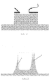
- Figures 1a to 1d illustrate schematically how the grass formation takes place as a consequence of extrusions remaining on the surface after grinding.
- ICP inductively coupled plasma
- ICP inductively coupled plasma
- ICP may also be referred to as 'TCP', Transformer coupled plasma.
- An ICP/TCP reactor is thus equipped with an RF source coupled to a coil through which the plasma is created.
- An ICP/TCP reactor may further be equipped with an RF or an LF source coupled to an electrode (as in a CCP reactor, see hereafter).
- CCP capacitive coupled plasma
- a CCP reactor is thus equipped with an RF power source (typically operating at 13.56MHz), coupled (through a capacitor) to one of the electrodes between which the plasma is created. Ions respond to the time-averaged potential over the capacitor, generally referred to as the DC-bias voltage (VDC) of the CCP reactor.
- VDC DC-bias voltage
- a CCP reactor may also be equipped with a Low Frequency source (for example operating at 113kHz).
- the root cause for the grass formation are Si-based extrusions originating from a not-perfectly polished surface. These extrusions hamper the DRIE etch, in such a way that sharp spikes are left on the surface after the DRIE process.
- the etch hampering mechanism is however not caused by the silicon extrusion itself because these will be readily etched but by the (unavoidable) formation of a native oxide around the extrusions (SiO x formation).
- SiO x formation native oxide around the extrusions
- These oxidized extrusions will act as a "micromask" during the subsequent dry etching process.
- the cause being the oxidized surface of the Silicon extrusions leading towards SiO x micromasks, has not been recognized before in the state of the art.
- Figures 1a-1d illustrate the problem.
- a silicon substrate 1 is shown in figure 1a , with a Si-extrusion 2 on the surface, left after the grinding step.
- a SiOx layer 3 is formed on the outer surface of the extrusion.
- Figure 1b illustrates the result of the first stages of the DRIE process. Due to the higher selectivity of the process to SiOx, the oxide layer is etched slower than the surrounding Si.
- an extrusion of the type shown in figure 1a represents two oxide layers 3a and 3b which need to be etched, due to the overhanging portion of the extrusion. This increases the difference in etching depth between the extrusion and the surrounding surface.
- the result, as illustrated in figures 1c and 1d is the formation of spikes 4 when the DRIE process is finished.
- the object of the invention is achieved by removing the oxidized surface of the extrusions using wet and/or dry etch processes.
- the above objective is accomplished by a method according to preferred embodiments described below.
- the method comprises at least a pre-cleaning step which is performed to remove at least part of the residues responsible for the micro masking effect that lead to the grass formation issue.
- This cleaning step may consist of a wet etch step or a dry etch step or a combination of both.
- a method for avoiding grass formation after grinding and during reactive ion etching is provided.
- the method of the invention is thus a method for producing 3D structures in a semiconductor substrate using DRIE, said method comprising at least the steps of:
- the substrate is a silicon wafer (semiconductor substrate). More preferably the substrate is a processed silicon wafer comprising active devices, on a front side. The substrate is preferably first bonded to a second substrate, before grinding the backside of the substrate.
- the step of grinding the backside of the substrate comprises a two step process.
- a rough grinding e.g. mesh 320
- an ultra fine grinding is performed to grind the last 20 ⁇ m. The ultra fine grind removes the deep mechanical damage from the rough step but does not remove the roughness of the substrate responsible for the grass formation.
- the surface treatment step may be performed using a wet etching step or a dry etching step.
- this step is preferably an immersion or spray or puddle etching of the substrate for a few minutes, preferably between 15s and 2min.
- the etching solution may be a solution comprising HNO 3 , HF and H 2 O or acetic acid, where the HNO 3 to HF ratio is preferably in the range 3:1 to 1:2 and the H 2 O and the acetic acid content is preferably at least the same as the other constituents.
- a typical example is a solution consisting of 1 part HNO 3 (65% conc.) 1 part HF (49%) and 2 parts H 2 O (or acetic acid) e.g. at 21°C [further referred to as "HNA” , B. Schwartz, H. Robbins, J. Electrochem. Soc. vol 123 (1976) 1903 ].
- a dry etching step said step is preferably performed using a CCP plasma or an ICP plasma (see definitions above). More preferably said dry etching is performed using an ICP or CCP plasma with a high degree of ion bombardment.
- the degree of ion bombardment may be expressed in terms of the ion energy, which is preferably situated between 100eV and 1000eV for the purpose of the present invention.
- these levels of ion bombardment may be obtained by applying an absolute value of the Bias voltage VDC, or of the LF component of the applied voltages, of 200V or higher, more preferably 400 or higher.
- VDC Bias voltage
- the dry-etch plasma used to perform the pre-cleaning contains one or more fluorine containing gases (e.g. SF6), possibly with one or more additive gases (e.g. Ar).
- the dry-etch plasma used to perform the pre-cleaning is an SF6 based CCP or ICP plasma for which the process time depends on the SiOx and Si removal rates of the process. This is typically between 1 and 10 minutes.
- SF6 based' means that the plasma takes place in a gas atmosphere consisting of SF6 and possibly additive gases such as Ar.
- the surface treatment step is performed using a combination of the above mentioned wet and dry etching steps.
- the step of performing deep reactive ion etching (DRIE) in order to achieve 3D vias is performed using a state of the art type of Bosch DRIE process (as described e.g. in patent document US-A-5501893 ), at an etch rate of approximately 2 ⁇ m/min.
- DRIE deep reactive ion etching
- Example of process recipe settings used on a CCP reactor Pressure SF6 flow Ar flow RF power Time mbar scm sccm W s 0.27 100 10 100 190
- the process time can vary depending on the etch rate and the dimensions of the extrusions, and is based on the experiment results.
- Example of process recipe settings used on a ICP reactor Pressure SF6 flow CF4 flow ICP Power BIAS power Time mTorr scm sccm W W s 5 100 180 1500 200 60
- the process time can vary depending on the etch rate and the dimensions of the extrusions, and is based on the experiment results.
- Example of the combination of the above mentioned wet and dry etching steps after the grinding, a plasma as in paragraph [0036] with a process time of only 1 minute is applied, followed by a 2 minutes HNA wet etching, again followed by a DI water rinse and an N2 dry step.
Landscapes
- Drying Of Semiconductors (AREA)
- Mechanical Treatment Of Semiconductor (AREA)
- Weting (AREA)
Abstract
- providing a substrate (1), and then
- grinding the backside of the substrate in order to achieve a thinned substrate, wherein extrusions (2) and native oxides (3) are left after said grinding step, and then
- performing a surface treatment selected from the group consisting of a wet etching step and a dry etching step in order to remove at least said native oxides (3) and extrusions (2) on the surface of said backside of the substrate which are causes for the grass formation during subsequent etching, and then
- performing deep reactive ion etching in order to achieve 3D vias.
Description
- The present invention is related to the field of semiconductor processing, in particular to the process known as Deep Reactive Ion Etching (DRIE), which is used to produce deep vias in a semiconductor (primarily Si) substrate. More particularly, the present invention is related to a surface treatment method after a grinding process step in order to avoid unwanted residuals which may lead to unwanted "grass formation" during the DRIE step.
- Deep reactive ion etching (DRIE) of Si is one of the most important process steps for fabrication of different sensors and actuators and for 3D integration. For some applications, the deep Si etching has to be carried out on thinned substrates, i.e. a second Si wafer is bonded to a first processed wafer and after this bonding, the wafer is thinned. This thinning process often consists of a first rough grinding step followed by a second (finer) grinding step. For some applications, a still finer polish process referred to as the final thinning step using Chemical Mechanical Polishing (CMP) is applied. However, if possible, this is avoided for cost (process time) and yield reasons. When this final thinning step is omitted, the subsequent Deep Reactive Ion Etching (DRIE), directly performed on ground surfaces, will suffer from the fact that even the smallest roughness caused by the ultra fine grinding processes can lead to detrimental effects on the DRIE, especially through so-called "grass formation". Grass formation is characterized as spear-shaped Si residues that are not etched as they should be. On ground wafers, grass formation occurs after DRIE (e.g. during etching of a deep via). The only known way of avoiding the extrusions, is by applying CMP prior to the DRIE process.
- It is an object of the invention to provide an easy and cost friendly solution to avoid grass formation and an alternative to the costly and time consuming CMP step and thereby avoiding the problem of grass formation. More particularly, it is an object of the invention to remove the cause of the micro-masking without applying a CMP step.
- The invention is related to a method as disclosed in the appended claims. In particular, the invention is related to a method for producing 3D structures in a semiconductor substrate using Deep Reactive Ion Etching (DRIE), comprising at least the steps of:
- providing a substrate,
- grinding the backside of the substrate in order to achieve a thinned substrate, wherein extrusions and native oxides are left after said grinding step,
- performing a surface treatment selected from the group consisting of a wet etching step and a dry etching step in order to remove at least said native oxides and extrusions on the surface of said backside of the substrate which are causes for the grass formation during subsequent etching,
- performing deep reactive ion etching in order to achieve 3D vias.
- The substrate may be a silicon wafer, more preferably a processed silicon wafer comprising active devices.
- According to an embodiment, the surface treatment step is a wet etching step performed by immersion, spray or puddle etching of the substrate in a solution comprising HNO3, HF and H2O or acetic acid, where the HNO3 (65% conc.) to HF (49% conc.) ratio is preferably in the range 3:1 to 1:2 and the H2O and the acetic acid content is preferably at least the same of the other constituents. Said solution may consist of 1 part HNO3 (65% conc.), 1part HF (49%) and 2 parts H2O. The wet etching step may be performed during a time interval of between 15 seconds and 2 minutes.
- According to another embodiment, the surface treatment step is a dry etching step performed using a CCP plasma or an ICP plasma. More particularly, the surface treatment step may be a dry etching step performed using an ICP or CCP plasma containing one or more fluorine containing gases (e.g. SF6), with optionally one or more additive gases (e.g. Ar).
- The surface treatment step may be a dry etching step performed using a CCP type reactor wherein the absolute value of the Bias voltage or of the LF component of the applied voltages is 200 V or higher. Also, the the surface treatment step may be a dry etching step performed using an ICP type reactor wherein the absolute value of the Bias voltage or of the LF component of the applied voltages, is 100 V or higher.
- The invention is also related to the use of the method according to the invention in DRIE etching of deep silicon structures (e.g. vias) in 3D integration of silicon wafers.
- It is an advantage of a method according to preferred embodiments that a supplementary time-consuming and expensive chemical mechanical polishing step after grinding can be avoided. It is a further advantage of the method according to preferred embodiments of the invention that no additional tool is needed and the surface treatment in order to prevent/avoid grass formation can be performed in the same (etch) chamber in which the subsequent DRIE etching of 3D structures is performed.
-
Figures 1a to 1d illustrate schematically how the grass formation takes place as a consequence of extrusions remaining on the surface after grinding. - The present invention will be described with respect to particular embodiments and with reference to certain drawings but the invention is not limited thereto but only by the claims. The drawings described are only schematic and are non-limiting. In the drawings, the size of some of the elements may be exaggerated and not drawn on scale for illustrative purposes. The dimensions and the relative dimensions do not correspond to actual reductions to practice of the invention.
- Moreover, the term top and the like in the description and the claims are used for descriptive purposes and not necessarily for describing relative positions. It is to be understood that the terms so used are interchangeable under appropriate circumstances and that the preferred embodiments described herein are capable of operation in other orientations than described or illustrated herein.
- It is to be noticed that the term "comprising", used in the claims, should not be interpreted as being restricted to the means listed thereafter; it does not exclude other elements or steps. It is thus to be interpreted as specifying the presence of the stated features, integers, steps or components as referred to, but does not preclude the presence or addition of one or more other features, integers, steps or components, or groups thereof. Thus, the scope of the expression "a device comprising means A and B" should not be limited to devices consisting only of components A and B. It means that with respect to the present invention, the only relevant components of the device are A and B.
- Reference throughout this specification to "one embodiment" or "an embodiment" means that a particular feature, structure or characteristic described in connection with the embodiment is included in at least one embodiment of the present invention. Thus, appearances of the phrases "in one embodiment" or "in an embodiment" in various places throughout this specification are not necessarily all referring to the same embodiment, but may. Furthermore, the particular features, structures or characteristics may be combined in any suitable manner, as would be apparent to one of ordinary skill in the art from this disclosure, in one or more embodiments.
- Furthermore, while some embodiments described herein include some but not other features included in other embodiments, combinations of features of different embodiments are meant to be within the scope of the invention, and form different embodiments, as would be understood by those in the art. For example, in the following claims, any of the claimed embodiments can be used in any combination.
- In the description provided herein, numerous specific details are set forth. However, it is understood that preferred embodiments may be practiced without these specific details. In other instances, well-known methods, structures and techniques have not been shown in detail in order not to obscure an understanding of this description.
- The term "ICP" as referred to in the claims and the description is used to define an inductively coupled plasma (ICP) and is referring to a type of plasma source in which the energy is supplied through a coil by radio frequent (typically 13.56 MHz) electrical currents which induce varying magnetic and electric fields, which deliver energy to the plasma. ICP may also be referred to as 'TCP', Transformer coupled plasma. An ICP/TCP reactor is thus equipped with an RF source coupled to a coil through which the plasma is created. An ICP/TCP reactor may further be equipped with an RF or an LF source coupled to an electrode (as in a CCP reactor, see hereafter).
- The term "CCP" as referred to in the claims and the description is used to define a capacitive coupled plasma (CCP) and is referring to a type of plasma source where radio frequent electric tensions/voltages are transferred through a capacitor to the plasma. One of two electrodes is connected to the power supply. A CCP reactor is thus equipped with an RF power source (typically operating at 13.56MHz), coupled (through a capacitor) to one of the electrodes between which the plasma is created. Ions respond to the time-averaged potential over the capacitor, generally referred to as the DC-bias voltage (VDC) of the CCP reactor. A CCP reactor may also be equipped with a Low Frequency source (for example operating at 113kHz).
- The invention will now be described by a detailed description of several preferred embodiments. It is clear that other preferred embodiments can be configured according to the knowledge of persons skilled in the art without departing from the true spirit or technical teaching of the invention as defined by the appended claims.
- The root cause for the grass formation are Si-based extrusions originating from a not-perfectly polished surface. These extrusions hamper the DRIE etch, in such a way that sharp spikes are left on the surface after the DRIE process. The etch hampering mechanism is however not caused by the silicon extrusion itself because these will be readily etched but by the (unavoidable) formation of a native oxide around the extrusions (SiOx formation). These oxidized extrusions will act as a "micromask" during the subsequent dry etching process. The cause, being the oxidized surface of the Silicon extrusions leading towards SiOx micromasks, has not been recognized before in the state of the art.
-
Figures 1a-1d illustrate the problem. Asilicon substrate 1 is shown infigure 1a , with a Si-extrusion 2 on the surface, left after the grinding step. ASiOx layer 3 is formed on the outer surface of the extrusion.Figure 1b illustrates the result of the first stages of the DRIE process. Due to the higher selectivity of the process to SiOx, the oxide layer is etched slower than the surrounding Si. Moreover, it can be seen that an extrusion of the type shown infigure 1a represents twooxide layers figures 1c and 1d , is the formation ofspikes 4 when the DRIE process is finished. - The object of the invention is achieved by removing the oxidized surface of the extrusions using wet and/or dry etch processes. The above objective is accomplished by a method according to preferred embodiments described below.
- According to preferred embodiments, the method comprises at least a pre-cleaning step which is performed to remove at least part of the residues responsible for the micro masking effect that lead to the grass formation issue. This cleaning step may consist of a wet etch step or a dry etch step or a combination of both.
- According to preferred embodiments a method for avoiding grass formation after grinding and during reactive ion etching is provided. The method of the invention is thus a method for producing 3D structures in a semiconductor substrate using DRIE, said method comprising at least the steps of:
- providing a substrate,
- grinding the backside of the substrate in order to achieve a thinned substrate,
- performing a surface treatment selected from at least one of a wet etching step and a dry etching step in order to remove at least the native oxides and extrusions on the surface of the substrate which are causes for the grass formation during subsequent etching,
- performing deep reactive ion etching in order to achieve 3D structures.
- According to preferred embodiments the substrate is a silicon wafer (semiconductor substrate). More preferably the substrate is a processed silicon wafer comprising active devices, on a front side. The substrate is preferably first bonded to a second substrate, before grinding the backside of the substrate.
- According to preferred embodiments, the step of grinding the backside of the substrate comprises a two step process. First, a rough grinding (e.g. mesh 320) is done to remove the bulk of the silicon. Then an ultra fine grinding is performed to grind the last 20 µm. The ultra fine grind removes the deep mechanical damage from the rough step but does not remove the roughness of the substrate responsible for the grass formation.
- As stated, the surface treatment step may be performed using a wet etching step or a dry etching step. In the case of a wet etching step, this step is preferably an immersion or spray or puddle etching of the substrate for a few minutes, preferably between 15s and 2min. The etching solution may be a solution comprising HNO3, HF and H2O or acetic acid, where the HNO3 to HF ratio is preferably in the range 3:1 to 1:2 and the H2O and the acetic acid content is preferably at least the same as the other constituents. A typical example is a solution consisting of 1 part HNO3 (65% conc.) 1 part HF (49%) and 2 parts H2O (or acetic acid) e.g. at 21°C [further referred to as "HNA" , B. Schwartz, H. Robbins, J. Electrochem. Soc. vol 123 (1976) 1903].
- In the case of a dry etching step, said step is preferably performed using a CCP plasma or an ICP plasma (see definitions above). More preferably said dry etching is performed using an ICP or CCP plasma with a high degree of ion bombardment.
- The degree of ion bombardment may be expressed in terms of the ion energy, which is preferably situated between 100eV and 1000eV for the purpose of the present invention. For a typical CCP type reactor, these levels of ion bombardment may be obtained by applying an absolute value of the Bias voltage VDC, or of the LF component of the applied voltages, of 200V or higher, more preferably 400 or higher.
- For a typical ICP/TCP type reactor the absolute value of the Bias voltage (VDC), or of the LF component of the applied voltages, has to be 100 V or higher.
- According to preferred embodiments, the dry-etch plasma used to perform the pre-cleaning contains one or more fluorine containing gases (e.g. SF6), possibly with one or more additive gases (e.g. Ar). According to preferred embodiments, the dry-etch plasma used to perform the pre-cleaning is an SF6 based CCP or ICP plasma for which the process time depends on the SiOx and Si removal rates of the process. This is typically between 1 and 10 minutes. 'SF6 based' means that the plasma takes place in a gas atmosphere consisting of SF6 and possibly additive gases such as Ar.
- According to preferred embodiments, the surface treatment step is performed using a combination of the above mentioned wet and dry etching steps.
- According to preferred embodiments, the step of performing deep reactive ion etching (DRIE) in order to achieve 3D vias is performed using a state of the art type of Bosch DRIE process (as described e.g. in patent document
US-A-5501893 ), at an etch rate of approximately 2 µm/min. Applying a traditional Bosch DRIE etch process to the ground wafers without performing the preceding surface treatment step resulted in a surface full of grass because the used Bosch process is very selective towards silicon oxide (i.e. the native oxide) which is formed onto the surface of the extrusions remaining after grinding. Because these extrusions act as a micromask during the Bosch DRIE process silicon pillars are formed during the Bosch DRIE (referred to as "grass formation"). - It is to be understood that although preferred embodiments, specific constructions and configurations, as well as materials, have been discussed herein for devices according to the present invention, various changes or modifications in form and detail may be made without departing from the scope of this invention as defined by the appended claims.
- Example of process recipe settings used on a CCP reactor:
Pressure SF6 flow Ar flow RF power Time mbar scm sccm W s 0.27 100 10 100 190 - Example of process recipe settings used on a ICP reactor:
Pressure SF6 flow CF4 flow ICP Power BIAS power Time mTorr scm sccm W W s 5 100 180 1500 200 60 - Example of process recipe settings used on a DSiE for a Bosch type process approach.
Priority Valve position SF6 flow CF4 flow ICP Power BIAS power BIAS on pulse BIAS off pulse step time % scm sccm W W % % s 1 100 0 350 1500 200 100 0 2 2 100 350 0 1500 200 100 0 5 - Example of the combination of the above mentioned wet and dry etching steps : after the grinding, a plasma as in paragraph [0036] with a process time of only 1 minute is applied, followed by a 2 minutes HNA wet etching, again followed by a DI water rinse and an N2 dry step.
Claims (10)
- A method for producing 3D structures in a semiconductor substrate using Deep Reactive Ion Etching (DRIE), comprising at least the steps of:- providing a substrate (1),- grinding the backside of the substrate in order to achieve a thinned substrate, wherein extrusions (2) and native oxides (3) are left after said grinding step,- performing a surface treatment selected from the group consisting of a wet etching step and a dry etching step in order to remove at least said native oxides (3) and extrusions (2) on the surface of said backside of the substrate which are causes for the grass formation during subsequent etching,- performing deep reactive ion etching in order to achieve 3D vias.
- The method according to claim 1 wherein the substrate (1) is a silicon wafer, more preferably a processed silicon wafer comprising active devices.
- The method according to claim 1 or 2, wherein the surface treatment step is a wet etching step performed by immersion, spray or puddle etching of the substrate in a solution comprising HNO3, HF and H2O or acetic acid, where the HNO3 (65% conc.) to HF (49% conc.) ratio is preferably in the range 3:1 to 1:2 and the H2O and the acetic acid content is preferably at least the same of the other constituents.
- The method according to claim 3, wherein said solution consists of 1 part HNO3 (65% conc.), 1part HF (49%) and 2 parts H2O.
- The method according to claim 3 or 4, wherein the wet etching step is performed during a time interval of between 15 seconds and 2 minutes.
- The method according to claim 1 wherein the surface treatment step is a dry etching step performed using a CCP plasma or an ICP plasma.
- The method according to claim 6 wherein the surface treatment step is a dry etching step performed using an ICP or CCP plasma containing one or more fluorine containing gases (e.g. SF6), with optionally one or more additive gases (e.g. Ar).
- The method according to claim 6 wherein the surface treatment step is a dry etching step performed using a CCP type reactor wherein the absolute value of the Bias voltage or of the LF component of the applied voltages is 200 V or higher.
- The method according to claim 6 wherein the surface treatment step is a dry etching step performed using an ICP type reactor wherein the absolute value of the Bias voltage or of the LF component of the applied voltages, is 100 V or higher.
- Use of the method according to claims 1 to 9 in DRIE etching of deep silicon structures (e.g. vias) in 3D integration of silicon wafers.
Applications Claiming Priority (1)
| Application Number | Priority Date | Filing Date | Title |
|---|---|---|---|
| US15542609P | 2009-02-25 | 2009-02-25 |
Publications (2)
| Publication Number | Publication Date |
|---|---|
| EP2224469A2 true EP2224469A2 (en) | 2010-09-01 |
| EP2224469A3 EP2224469A3 (en) | 2015-03-25 |
Family
ID=42211922
Family Applications (1)
| Application Number | Title | Priority Date | Filing Date |
|---|---|---|---|
| EP10154439.3A Withdrawn EP2224469A3 (en) | 2009-02-25 | 2010-02-23 | Method for etching 3d structures in a semiconductor substrate, including surface preparation |
Country Status (2)
| Country | Link |
|---|---|
| US (1) | US20100216308A1 (en) |
| EP (1) | EP2224469A3 (en) |
Cited By (1)
| Publication number | Priority date | Publication date | Assignee | Title |
|---|---|---|---|---|
| US9006703B2 (en) | 2013-07-31 | 2015-04-14 | International Business Machines Corporation | Method for reducing lateral extrusion formed in semiconductor structures and semiconductor structures formed thereof |
Families Citing this family (3)
| Publication number | Priority date | Publication date | Assignee | Title |
|---|---|---|---|---|
| MD360Z (en) * | 2010-09-23 | 2011-11-30 | Институт Прикладной Физики Академии Наук Молдовы | Process for the formation of microstructured surfaces of silicon substrates |
| JP2013084695A (en) * | 2011-10-06 | 2013-05-09 | Tokyo Electron Ltd | Semiconductor device manufacturing method |
| KR102663833B1 (en) * | 2017-02-10 | 2024-05-03 | 어플라이드 머티어리얼스, 인코포레이티드 | Method and apparatus for low temperature selective epitaxy in a deep trench |
Citations (1)
| Publication number | Priority date | Publication date | Assignee | Title |
|---|---|---|---|---|
| US5501893A (en) | 1992-12-05 | 1996-03-26 | Robert Bosch Gmbh | Method of anisotropically etching silicon |
Family Cites Families (12)
| Publication number | Priority date | Publication date | Assignee | Title |
|---|---|---|---|---|
| US2619414A (en) * | 1950-05-25 | 1952-11-25 | Bell Telephone Labor Inc | Surface treatment of germanium circuit elements |
| US5204288A (en) * | 1988-11-10 | 1993-04-20 | Applied Materials, Inc. | Method for planarizing an integrated circuit structure using low melting inorganic material |
| JP3612158B2 (en) * | 1996-11-18 | 2005-01-19 | スピードファム株式会社 | Plasma etching method and apparatus |
| WO2000072366A1 (en) * | 1999-05-21 | 2000-11-30 | Plasmasil, L.L.C. | Method for improving thickness uniformity of semiconductor wafers |
| US6794272B2 (en) * | 2001-10-26 | 2004-09-21 | Ifire Technologies, Inc. | Wafer thinning using magnetic mirror plasma |
| US6846747B2 (en) * | 2002-04-09 | 2005-01-25 | Unaxis Usa Inc. | Method for etching vias |
| US6818532B2 (en) * | 2002-04-09 | 2004-11-16 | Oriol, Inc. | Method of etching substrates |
| US8278738B2 (en) * | 2005-02-17 | 2012-10-02 | Sharp Kabushiki Kaisha | Method of producing semiconductor device and semiconductor device |
| JP4817291B2 (en) * | 2005-10-25 | 2011-11-16 | Okiセミコンダクタ株式会社 | Manufacturing method of semiconductor wafer |
| US7608837B2 (en) * | 2006-11-24 | 2009-10-27 | Tower Semiconductor Ltd. | High resolution integrated X-ray CMOS image sensor |
| US7863189B2 (en) * | 2007-01-05 | 2011-01-04 | International Business Machines Corporation | Methods for fabricating silicon carriers with conductive through-vias with low stress and low defect density |
| JP4799542B2 (en) * | 2007-12-27 | 2011-10-26 | 株式会社東芝 | Semiconductor package |
-
2010
- 2010-02-23 EP EP10154439.3A patent/EP2224469A3/en not_active Withdrawn
- 2010-02-24 US US12/711,544 patent/US20100216308A1/en not_active Abandoned
Patent Citations (1)
| Publication number | Priority date | Publication date | Assignee | Title |
|---|---|---|---|---|
| US5501893A (en) | 1992-12-05 | 1996-03-26 | Robert Bosch Gmbh | Method of anisotropically etching silicon |
Non-Patent Citations (1)
| Title |
|---|
| B. SCHWARTZ; H. ROBBINS, J. ELECTROCHEM. SOC., vol. 123, 1976, pages 1903 |
Cited By (1)
| Publication number | Priority date | Publication date | Assignee | Title |
|---|---|---|---|---|
| US9006703B2 (en) | 2013-07-31 | 2015-04-14 | International Business Machines Corporation | Method for reducing lateral extrusion formed in semiconductor structures and semiconductor structures formed thereof |
Also Published As
| Publication number | Publication date |
|---|---|
| US20100216308A1 (en) | 2010-08-26 |
| EP2224469A3 (en) | 2015-03-25 |
Similar Documents
| Publication | Publication Date | Title |
|---|---|---|
| US8617962B2 (en) | Method for finishing a substrate of the semiconductor-on-insulator type | |
| US10629473B2 (en) | Footing removal for nitride spacer | |
| US10242908B2 (en) | Airgap formation with damage-free copper | |
| TWI753010B (en) | Poly directional etch by oxidation | |
| US7776719B2 (en) | Method for manufacturing bonded wafer | |
| US6846746B2 (en) | Method of smoothing a trench sidewall after a deep trench silicon etch process | |
| US6287974B1 (en) | Method of achieving top rounding and uniform etch depths while etching shallow trench isolation features | |
| US20180138049A1 (en) | SiN SPACER PROFILE PATTERNING | |
| US20060043066A1 (en) | Processes for pre-tapering silicon or silicon-germanium prior to etching shallow trenches | |
| US8357587B2 (en) | Method for routing a chamfered substrate | |
| US6235640B1 (en) | Techniques for forming contact holes through to a silicon layer of a substrate | |
| US20130157470A1 (en) | Plasma etching method | |
| WO1999067817A1 (en) | Silicon trench etching using silicon-containing precursors to reduce or avoid mask erosion | |
| US20100216308A1 (en) | Method for etching 3d structures in a semiconductor substrate, including surface preparation | |
| US7253083B2 (en) | Method of thinning a semiconductor structure | |
| EP1538663A3 (en) | Wafer backside processing method and corresponding processing apparatus | |
| US9082819B2 (en) | Process for thinning the active silicon layer of a substrate of “silicon on insulator” (SOI) type | |
| TWI570804B (en) | A method of forming a notch at the bottom of the hole during the etching process, and a method of forming the hole | |
| US6709984B2 (en) | Method for manufacturing semiconductor device | |
| KR20160023712A (en) | Method for manufacturing bonded wafer | |
| KR101794738B1 (en) | Plasma processing method | |
| CN102386084B (en) | Method for planarizing surface of wafer | |
| EP4576172A1 (en) | Methods of treating a semiconductor substrate and apparatus | |
| US20260033259A1 (en) | Method of plasma dicing a semiconductor wafer | |
| JP5171091B2 (en) | Plasma processing method |
Legal Events
| Date | Code | Title | Description |
|---|---|---|---|
| PUAI | Public reference made under article 153(3) epc to a published international application that has entered the european phase |
Free format text: ORIGINAL CODE: 0009012 |
|
| AK | Designated contracting states |
Kind code of ref document: A2 Designated state(s): AT BE BG CH CY CZ DE DK EE ES FI FR GB GR HR HU IE IS IT LI LT LU LV MC MK MT NL NO PL PT RO SE SI SK SM TR |
|
| AX | Request for extension of the european patent |
Extension state: AL BA RS |
|
| PUAL | Search report despatched |
Free format text: ORIGINAL CODE: 0009013 |
|
| AK | Designated contracting states |
Kind code of ref document: A3 Designated state(s): AT BE BG CH CY CZ DE DK EE ES FI FR GB GR HR HU IE IS IT LI LT LU LV MC MK MT NL NO PL PT RO SE SI SK SM TR |
|
| AX | Request for extension of the european patent |
Extension state: AL BA RS |
|
| RIC1 | Information provided on ipc code assigned before grant |
Ipc: H01L 21/3065 20060101ALI20150218BHEP Ipc: H01L 21/304 20060101AFI20150218BHEP |
|
| STAA | Information on the status of an ep patent application or granted ep patent |
Free format text: STATUS: THE APPLICATION IS DEEMED TO BE WITHDRAWN |
|
| 18D | Application deemed to be withdrawn |
Effective date: 20150926 |