EP2223807A1 - Method of manufacturing a substrate for a liquid discharge head - Google Patents
Method of manufacturing a substrate for a liquid discharge head Download PDFInfo
- Publication number
- EP2223807A1 EP2223807A1 EP10154893A EP10154893A EP2223807A1 EP 2223807 A1 EP2223807 A1 EP 2223807A1 EP 10154893 A EP10154893 A EP 10154893A EP 10154893 A EP10154893 A EP 10154893A EP 2223807 A1 EP2223807 A1 EP 2223807A1
- Authority
- EP
- European Patent Office
- Prior art keywords
- silicon substrate
- layer
- silicon
- groove
- substrate
- Prior art date
- Legal status (The legal status is an assumption and is not a legal conclusion. Google has not performed a legal analysis and makes no representation as to the accuracy of the status listed.)
- Granted
Links
- 239000000758 substrate Substances 0.000 title claims abstract description 155
- 238000004519 manufacturing process Methods 0.000 title claims abstract description 44
- 239000007788 liquid Substances 0.000 title claims abstract description 32
- 229910052710 silicon Inorganic materials 0.000 claims abstract description 159
- 239000010703 silicon Substances 0.000 claims abstract description 159
- XUIMIQQOPSSXEZ-UHFFFAOYSA-N Silicon Chemical compound [Si] XUIMIQQOPSSXEZ-UHFFFAOYSA-N 0.000 claims abstract description 158
- 238000001039 wet etching Methods 0.000 claims abstract description 7
- 238000000034 method Methods 0.000 claims description 23
- WGTYBPLFGIVFAS-UHFFFAOYSA-M tetramethylammonium hydroxide Chemical compound [OH-].C[N+](C)(C)C WGTYBPLFGIVFAS-UHFFFAOYSA-M 0.000 claims description 18
- VYPSYNLAJGMNEJ-UHFFFAOYSA-N Silicium dioxide Chemical compound O=[Si]=O VYPSYNLAJGMNEJ-UHFFFAOYSA-N 0.000 claims description 13
- 230000001678 irradiating effect Effects 0.000 claims description 5
- 229910052814 silicon oxide Inorganic materials 0.000 claims description 3
- 229910052581 Si3N4 Inorganic materials 0.000 claims description 2
- 239000007864 aqueous solution Substances 0.000 claims description 2
- 238000007254 oxidation reaction Methods 0.000 claims description 2
- 230000001590 oxidative effect Effects 0.000 claims description 2
- HQVNEWCFYHHQES-UHFFFAOYSA-N silicon nitride Chemical compound N12[Si]34N5[Si]62N3[Si]51N64 HQVNEWCFYHHQES-UHFFFAOYSA-N 0.000 claims description 2
- 238000005530 etching Methods 0.000 description 82
- 239000010410 layer Substances 0.000 description 80
- 230000001681 protective effect Effects 0.000 description 23
- 229920001709 polysilazane Polymers 0.000 description 7
- 230000008569 process Effects 0.000 description 6
- 229910052681 coesite Inorganic materials 0.000 description 5
- 229910052906 cristobalite Inorganic materials 0.000 description 5
- 239000000377 silicon dioxide Substances 0.000 description 5
- 229910052682 stishovite Inorganic materials 0.000 description 5
- 229910052905 tridymite Inorganic materials 0.000 description 5
- 230000015572 biosynthetic process Effects 0.000 description 4
- 238000001312 dry etching Methods 0.000 description 4
- 238000000206 photolithography Methods 0.000 description 4
- LIVNPJMFVYWSIS-UHFFFAOYSA-N silicon monoxide Chemical compound [Si-]#[O+] LIVNPJMFVYWSIS-UHFFFAOYSA-N 0.000 description 4
- 239000013078 crystal Substances 0.000 description 3
- 238000010304 firing Methods 0.000 description 3
- 238000000059 patterning Methods 0.000 description 3
- 239000011241 protective layer Substances 0.000 description 3
- 238000007796 conventional method Methods 0.000 description 2
- 238000007599 discharging Methods 0.000 description 2
- 239000000428 dust Substances 0.000 description 2
- 239000000463 material Substances 0.000 description 2
- 230000009467 reduction Effects 0.000 description 2
- 229920002614 Polyether block amide Polymers 0.000 description 1
- 229910003814 SiH2NH Inorganic materials 0.000 description 1
- 229910004200 TaSiN Inorganic materials 0.000 description 1
- ATJFFYVFTNAWJD-UHFFFAOYSA-N Tin Chemical compound [Sn] ATJFFYVFTNAWJD-UHFFFAOYSA-N 0.000 description 1
- 239000008186 active pharmaceutical agent Substances 0.000 description 1
- 239000000853 adhesive Substances 0.000 description 1
- 230000001070 adhesive effect Effects 0.000 description 1
- PNEYBMLMFCGWSK-UHFFFAOYSA-N aluminium oxide Inorganic materials [O-2].[O-2].[O-2].[Al+3].[Al+3] PNEYBMLMFCGWSK-UHFFFAOYSA-N 0.000 description 1
- 230000008901 benefit Effects 0.000 description 1
- 230000007547 defect Effects 0.000 description 1
- 230000000994 depressogenic effect Effects 0.000 description 1
- 230000000694 effects Effects 0.000 description 1
- 238000009429 electrical wiring Methods 0.000 description 1
- XLYOFNOQVPJJNP-ZSJDYOACSA-N heavy water Substances [2H]O[2H] XLYOFNOQVPJJNP-ZSJDYOACSA-N 0.000 description 1
- 239000002184 metal Substances 0.000 description 1
- 229910052751 metal Inorganic materials 0.000 description 1
- 238000012986 modification Methods 0.000 description 1
- 230000004048 modification Effects 0.000 description 1
- 150000003376 silicon Chemical class 0.000 description 1
- 238000004528 spin coating Methods 0.000 description 1
- 238000004544 sputter deposition Methods 0.000 description 1
- XLYOFNOQVPJJNP-UHFFFAOYSA-N water Substances O XLYOFNOQVPJJNP-UHFFFAOYSA-N 0.000 description 1
Images


Classifications
-
- B—PERFORMING OPERATIONS; TRANSPORTING
- B41—PRINTING; LINING MACHINES; TYPEWRITERS; STAMPS
- B41J—TYPEWRITERS; SELECTIVE PRINTING MECHANISMS, i.e. MECHANISMS PRINTING OTHERWISE THAN FROM A FORME; CORRECTION OF TYPOGRAPHICAL ERRORS
- B41J2/00—Typewriters or selective printing mechanisms characterised by the printing or marking process for which they are designed
- B41J2/005—Typewriters or selective printing mechanisms characterised by the printing or marking process for which they are designed characterised by bringing liquid or particles selectively into contact with a printing material
- B41J2/01—Ink jet
- B41J2/135—Nozzles
- B41J2/16—Production of nozzles
- B41J2/1621—Manufacturing processes
- B41J2/1626—Manufacturing processes etching
- B41J2/1629—Manufacturing processes etching wet etching
-
- B—PERFORMING OPERATIONS; TRANSPORTING
- B41—PRINTING; LINING MACHINES; TYPEWRITERS; STAMPS
- B41J—TYPEWRITERS; SELECTIVE PRINTING MECHANISMS, i.e. MECHANISMS PRINTING OTHERWISE THAN FROM A FORME; CORRECTION OF TYPOGRAPHICAL ERRORS
- B41J2/00—Typewriters or selective printing mechanisms characterised by the printing or marking process for which they are designed
- B41J2/005—Typewriters or selective printing mechanisms characterised by the printing or marking process for which they are designed characterised by bringing liquid or particles selectively into contact with a printing material
- B41J2/01—Ink jet
- B41J2/135—Nozzles
- B41J2/16—Production of nozzles
- B41J2/1601—Production of bubble jet print heads
- B41J2/1603—Production of bubble jet print heads of the front shooter type
-
- B—PERFORMING OPERATIONS; TRANSPORTING
- B41—PRINTING; LINING MACHINES; TYPEWRITERS; STAMPS
- B41J—TYPEWRITERS; SELECTIVE PRINTING MECHANISMS, i.e. MECHANISMS PRINTING OTHERWISE THAN FROM A FORME; CORRECTION OF TYPOGRAPHICAL ERRORS
- B41J2/00—Typewriters or selective printing mechanisms characterised by the printing or marking process for which they are designed
- B41J2/005—Typewriters or selective printing mechanisms characterised by the printing or marking process for which they are designed characterised by bringing liquid or particles selectively into contact with a printing material
- B41J2/01—Ink jet
- B41J2/135—Nozzles
- B41J2/16—Production of nozzles
- B41J2/1621—Manufacturing processes
- B41J2/1631—Manufacturing processes photolithography
-
- B—PERFORMING OPERATIONS; TRANSPORTING
- B41—PRINTING; LINING MACHINES; TYPEWRITERS; STAMPS
- B41J—TYPEWRITERS; SELECTIVE PRINTING MECHANISMS, i.e. MECHANISMS PRINTING OTHERWISE THAN FROM A FORME; CORRECTION OF TYPOGRAPHICAL ERRORS
- B41J2/00—Typewriters or selective printing mechanisms characterised by the printing or marking process for which they are designed
- B41J2/005—Typewriters or selective printing mechanisms characterised by the printing or marking process for which they are designed characterised by bringing liquid or particles selectively into contact with a printing material
- B41J2/01—Ink jet
- B41J2/135—Nozzles
- B41J2/16—Production of nozzles
- B41J2/1621—Manufacturing processes
- B41J2/1632—Manufacturing processes machining
- B41J2/1634—Manufacturing processes machining laser machining
Definitions
- the present invention relates to a manufacturing method of a liquid discharge head substrate (a substrate for a liquid discharge head), and in particular relates to a manufacturing method of substrate for an ink jet recording head for use in an ink jet recording head that discharges ink onto a recording medium to perform recording.
- a liquid discharge head is an ink jet recording head that discharges ink as liquid droplets onto a recording medium (typically, paper) by energy to perform recording.
- a recording medium typically, paper
- energy generating elements that are mounted on a surface of a substrate are supplied with ink from an opposite surface of the substrate via a supply port passing from the opposite surface through to the surface.
- a manufacturing method of a substrate for this type of ink jet recording head is disclosed in U.S. Patent Application No. 2007/0212890 .
- an opening is formed in an etching mask layer on an opposite surface of a silicon substrate, a depression is formed in silicon exposed in the opening by dry etching, a laser, or the like, and the silicon substrate is wet etched from the depression to form a supply port that passes through the substrate.
- the opening is formed in an entire area of the opposite surface of the substrate corresponding to the supply port, which requires patterning to be performed on the etching mask layer. A photolithography process is necessary for this operation.
- the present invention has an advantage of providing a method of manufacturing a substrate for a liquid discharge head according to which an ink supply port can be formed simply and in a relatively short time.
- the present invention provides a method of manufacturing a substrate for a liquid discharging head as set out in claim 1.
- an ink supply port can be formed in a relatively short time.
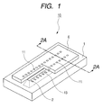
- FIG. 1 is a perspective view illustrating a structure of an ink jet recording head according to a first embodiment.
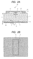
- FIGS. 2A and 2B are views for describing a manufacturing method of the ink jet recording head according to the first embodiment.
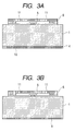
- FIGS. 3A and 3B are views for describing the manufacturing method of the ink jet recording head according to the first embodiment.
- FIGS. 4A and 4B are views illustrating a state during a manufacturing process in the manufacturing method of the ink jet recording head according to the first embodiment.
- FIGS. 5A and 5B are views for describing a state during the manufacturing process in the manufacturing method of the ink jet recording head according to the first embodiment.
- FIGS. 6A, 6B, 6C, 6D, 6E and 6F are views for describing a state during the manufacturing process in the manufacturing method of the ink jet recording head according to the first embodiment.
- FIGS. 7A and 7B are views illustrating a state during a manufacturing process in a manufacturing method of an ink jet recording head according to a second embodiment.
- FIGS. 8A, 8B, 8C, 8D and 8E are views illustrating a state during the manufacturing process in the manufacturing method of the ink jet recording head according to the second embodiment.
- an ink jet recording head is used as an example of a liquid discharge head
- an ink jet recording head substrate is used as an example of a liquid discharge head substrate.
- the present invention is not limited to such.
- the liquid discharge head is applicable not only in printing fields but also in various industrial fields such as circuit formation, and the liquid discharge head substrate is usable as a substrate installed in such a liquid discharge head.
- FIG. 1 is a perspective view illustrating an ink jet recording head according to a first embodiment of the present invention.
- An ink jet recording head 10 illustrated in FIG. 1 includes a silicon substrate 1 on which energy generating elements 2 for generating energy used to discharge a liquid such as ink are arranged at a predetermined pitch in two rows.
- a polyether amide layer (not illustrated) is formed on the silicon substrate 1 as an adhesion layer.
- an organic film layer 6 that includes a flow path side wall and ink discharge ports 11 located above the energy generating elements 2 is formed on the silicon substrate 1.
- an ink supply port 13 is formed in the silicon substrate 1 between the rows of the energy generating elements 2.
- an ink flow path communicating from the ink supply port 13 to each ink discharge port 11 is formed.
- the ink jet recording head 10 is positioned so that its surface on which the ink discharge ports 11 are formed faces a recording surface of a recording medium.
- the energy generating elements 2 apply pressure to ink (liquid) that is filled in the ink flow path from the ink supply port 13, droplets of ink are discharged from the ink discharge ports 11. These droplets of ink are deposited on the recording medium, as a result of which an image is formed.
- the term "to form an image” includes not only an instance of forming an image having some meaning such as characters, figures, and signs, but also an instance of forming an image having no specific meaning such as geometrical patterns.
- an etching mask layer is processed by a laser, dry etching, or the like to create a frame pattern for forming an opening of the ink supply port, and then crystal anisotropic etching is performed.
- FIGS. 3A and 3B are sectional views for describing the manufacturing method of the ink jet recording head 10, taken along the section line 2A-2A in Fig. 1 .
- FIG. 2A is a sectional view taken along the section line 2A-2A in FIG. 1 and
- FIG. 2B is a plan view of an opposite surface (second surface) of the silicon substrate 1. Note that FIG. 2A illustrates a state before the ink supply port 13 is formed.
- FIG. 4A is a sectional view taken along the section line 2A-2A in FIG. 1
- FIG. 4B is a plan view of the opposite surface (second surface) of the silicon substrate 1.
- FIGS. 2A, 2B , 4A, and 4B illustrate a state before the ink supply port 13 is formed.
- the silicon substrate 1 having the organic film layer 6 as a discharge port member provided with the discharge ports 11 is prepared.
- the energy generating elements 2 are arranged in two rows along a longitudinal direction of the silicon substrate 1, on the surface of the silicon substrate 1.
- the energy generating elements 2 are composed of wiring made of Al or the like, a high-resistance material such as TaSiN or TaN, and so on.
- a sacrificial layer 5 for specifying an opening width of the ink supply port 13 on the surface side can be formed on the surface of the silicon substrate 1.
- Al as a material of the sacrificial layer 5 is efficient because the sacrificial layer 5 can be formed at the same time as wiring.
- an insulating protective film 3 (see e.g. Fig. 2A ) is formed so as to cover the energy generating elements 2 and the sacrificial layer 5.
- the insulating protective film 3 is made of SiO, SiN, or the like.
- the insulating protective film 3 protects the wiring formed on the silicon substrate 1 from ink and other liquids, and also serves as an etching stop layer when forming the ink supply port 13.
- the adhesion layer (not illustrated) and the organic film layer 6 are provided on the insulating protective film 3 using a photolithography process, thereby forming the ink flow path and the ink discharge ports 11.
- the silicon substrate 1 also has an etching mask layer 4 on its opposite surface.
- An etching rate of the etching mask layer 4 to an etchant of silicon is lower than an etching rate of silicon to the etchant.
- the etching mask layer 4 can be sufficiently resistant to the etchant of silicon, and at least one layer of the etching mask layer 4 is formed on the opposite surface of the silicon substrate 1.
- an insulating film such as SiO, a metal film such as Mo, Au, TiN, or Ti, an inorganic film, and an organic film are formed as the etching mask layer 4.
- the use of a thermal oxide film of SiO contributes to a shorter manufacturing time, since it can be formed at the same time as the insulating protective film 3 on the surface.
- a protective film 16 that, even when a pinhole (not illustrated) is present, can cover such a pinhole may be formed.
- selection can be made from films such as an organic film and an inorganic film.
- a silicon-based film such as SiO, SiO 2 , SiN, or SiC is suitable.
- a formation method may be a well known method such as spin coating or sputtering.
- a SiO 2 film is formed on the etching mask layer 4 by firing using polysilazane as the protective film 16 of a TMAH (tetramethyl ammonium hydroxide) etchant, which is applicable to the present invention.
- Polysilazane forms a SiO 2 film by reacting with water in air, as shown by Formula 1.
- the protective film 16 is preferably made of SiO 2 and polysilazane is preferably used in the formation of the protective film.
- An etching resistance increases when a firing temperature is higher. In consideration of an etching time, firing at 250°C or higher is suitable.
- FIG. 3B Alternatively, a structure of not providing the protecting film 16 may be adopted as illustrated in FIG. 3B .
- a groove 7 having a rectangular frame shape as illustrated in FIG. 2B is formed in a portion of the etching mask layer 4 corresponding to the ink supply port 13, by removing the protective layer 16 and the etching mask layer 4 with a laser.
- One such frame corresponds to one supply port 13.
- Silicon exposed in a frame shape as a result of removing the protective layer 16 and the etching mask layer 4 encloses the protective layer 16 and the etching mask layer 4 in the inside of the frame.
- laser processing is performed from over the protective film 16.
- a third harmonic wave (a wavelength of 355 nm) of a YAG laser with excellent absorptivity to silicon is used as a laser source, and the groove 7 is formed under conditions of an output of about 4.5 W and a frequency of about 30 kHz.
- the groove 7 in a frame shape is formed so as to pass through the etching mask layer 4 and has a depth of about 10 ⁇ m from the opposite surface of the silicon substrate 1.
- the groove 7 is provided in the silicon substrate 1 so as to pass through only the mask layer 4, as illustrated in FIG. 4A .
- FIGS. 2A and 4A are defined as follows.
- t denotes a thickness of the etching mask layer 4
- T denotes a thickness of the silicon substrate 1.
- X denotes a lateral distance from a longitudinal center line 14 of the silicon substrate 1 to a center of the groove 7 (so not the center of the frame itself).
- L denotes a width of the sacrificial layer 5, which is a width of an opening of the ink supply port 13 on the surface of the silicon substrate 1 in a lateral direction of the silicon substrate 1.
- D denotes a depth of the groove 7 toward the substrate.
- the thickness T of the silicon substrate 1 is about 600 ⁇ m to 750 ⁇ m, and the depth of the groove 7 is about 5 ⁇ m to 20 ⁇ m.
- silicon may be exposed by only removing the mask layer 4 in a frame shape by a laser. So long as silicon is exposed, etching from the opposite surface to the surface can be performed using a silicon etchant.
- FIGS. 5A and 5B are views illustrating another pattern of the groove 7.
- FIG. 5A is a sectional view taken along the section line 2A-2A in FIG. 1
- FIG. 5B is a plan view of the opposite surface of the silicon substrate 1 covered with the etching mask layer 4.
- the groove 7 may be formed not in a frame shape as illustrated in FIG. 2B , but in a lattice (or ladder) shape as illustrated in FIG. 5B .
- Opposing side portions 7d of the groove 7 are situated inside outermost frame portions 7a (which form a rectangle), thereby forming a lattice shape.
- lateral portions 7c (whose length is denoted by Q) that are connected with longitudinal portions 7b (whose length is denoted by R) extending in the longitudinal direction of the substrate 1 are approximately parallel to the opposing side portions 7d, and the opposing side portions 7d are connected with the longitudinal portions 7b as with the lateral portions 7c.
- a laser processing time and an etching rate in an etching operation described later vary according to a pitch P of the groove 7 in the longitudinal direction of the silicon substrate 1 illustrated in FIG. 5B (so vary according to the distance between lateral portions of the groove).
- Table 1 indicates relationships of the etching rate and the laser processing time with respect to the pitch P of the groove 7 in the longitudinal direction of the silicon substrate 1, in the case of adopting the shape of the groove 7 illustrated in FIGS. 5A and 5B in the manufacturing method of this embodiment.
- R 15200 ⁇ m
- Q 700 ⁇ m.
- the etching rate is designated as A when a ⁇ 100 ⁇ surface which is one of the surface orientations of silicon can be formed in 10 hours in the etching operation described later.
- the etching rate is designated as B when, though the ⁇ 100 ⁇ surface cannot be formed in 10 hours in the etching operation, the ⁇ 100 ⁇ surface can be formed when etching proceeds to the sacrificial layer 5.
- the laser processing time is designated as A when the time required for forming the groove 7 is not longer than (so less than or equal to) twice the time of forming the frame-shaped groove 7 illustrated in FIG. 2B , and designated as B when the time required for forming the groove 7 is longer than twice the time of forming the frame-shaped groove 7.
- the pitch P when the pitch P is smaller, the laser processing time is longer but the etching time is shorter. Accordingly, for a same level of etching rate as conventional, the pitch P can be set to not more than 800 ⁇ m. Furthermore, the pitch P is preferably set to 600 ⁇ m to 800 ⁇ m, when also taking the laser processing time into consideration.
- the groove 7 is not limited to the shape partitioned in the longitudinal direction of the silicon substrate 1 as illustrated in FIG. 5B , and may have a shape partitioned in the lateral direction.
- the depth D of the groove 7 preferably satisfies the following relational expression (1) (see FIG. 2A ).
- t denotes the thickness of the etching mask layer 4
- T denotes the thickness of the silicon substrate 1.
- X denotes the distance from the longitudinal center line 14 of the silicon substrate 1 to the center of the groove 7 formed along the center line 14.
- L denotes the width of the sacrificial layer 5 in the lateral direction of the silicon substrate 1.
- an etched area is contained within the area of the sacrificial layer 5, so that the opening width of the opening of the ink supply port 13 on the surface of the silicon substrate 1 can be set to the width L of the sacrificial layer 5.
- the width L of the sacrificial layer 5 is sufficiently large and (X - L/2) becomes a negative value.
- the etched area reaches into the sacrificial layer 5 regardless of the values of T and t.
- the expression (1) is satisfied even in this case.
- the etching operation of forming the ink supply port 13 by passing through the silicon substrate 1 from the groove 7 to the sacrificial layer 5 by crystal anisotropic etching is performed.
- TMAH tetramethyl ammonium hydroxide
- FIGS. 6A to 6F are views illustrating the internal state of the silicon substrate 1 in the etching operation in the first embodiment.
- ⁇ 111 ⁇ surfaces 21a, 21b, 21c, and 21d which are one of the surface orientations of silicon, are formed so as to decrease in width in a direction from the opposite surface toward the surface of the silicon substrate 1.
- the dotted areas indicate the original position of the groove 7.
- the etching mask layer 4 is etched in a direction perpendicular to the thickness direction of the silicon substrate 1 (see FIG. 6A ).
- the etching mask layer 4 remaining between the groove 7 is etched, and a ⁇ 100 ⁇ surface 22 is formed between the groove 7 (see FIG. 6C ).
- the ⁇ 100 ⁇ surface 22 moves toward the surface of the silicon substrate 1 (see FIG. 6D ), and eventually reaches the sacrificial layer 5.
- the ink supply port 13 is formed in an etching time of 1450 minutes.
- Whether or not to remove the protective film 16 can be selected in consideration of, for example, compatibility between the protective film 16 and an adhesive that is applied to the opposite surface side of the silicon substrate 1 when bonding the opposite surface side to a support member of alumina or the like for supporting the silicon substrate 1, upon assembly of the ink jet recording head.
- the silicon substrate 1 (ink jet recording head substrate) where a nozzle portion for discharging, from the ink discharge ports 11, ink flowing from the ink supply port 13 is formed is completed.
- This silicon substrate 1 is cut and separated into chips by a dicing saw or the like. After electrical wiring for driving the energy generating elements 2 is performed on each chip, a chip tank member for ink supply is connected. This completes the ink jet recording head 10.
- a time reduction of 240 minutes per lot (or batch) can be achieved when compared with a conventional method of performing a patterning operation of the etching mask layer 4 by a photolithography process.
- FIGS. 7A and 7B are views for describing a manufacturing method of an ink jet recording head in this embodiment.
- FIG. 7A is a sectional view of an ink jet recording head in this embodiment, taken along a section line corresponding to the section line 2A-2A in FIG. 1 .
- FIG. 7B is a plan view of the opposite surface of the silicon substrate 1 in the ink jet recording head. Note that the same structures as the ink jet recording head 10 described in the first embodiment are given the same numerals and their detailed description is omitted. Moreover, the ink jet recording head is the same as the ink jet recording head 10 in the surface structure of the silicon substrate 1 and the above-mentioned layering process, and so their description is omitted, too.
- the groove 7 is formed in a lattice shape in a laser processing operation. This is the same as the one described in the first embodiment. That is, in the groove 7, the opposing side portions 7d are situated inside the outermost frame portions 7a, thereby forming a lattice shape.
- the lateral portions 7c (whose length is denoted by Q) that are connected with the longitudinal portions 7b (whose length is denoted by R) extending in the longitudinal direction of the silicon substrate 1 are approximately parallel to the opposing side portions 7d, and the opposing side portions 7d are connected with the longitudinal portions 7b as with the lateral portions 7c.
- leading holes 8 as deep depressions illustrated in FIG. 7A are formed within the area enclosed by the outermost frame portions 7a of the groove 7.
- the leading holes 8 are non-through holes that pass through the etching mask layer 4 and the protective film 16 but end inside the silicon substrate 1.
- part of the opposing side portions 7d is the leading holes 8.
- the leading holes 8 are arranged in two rows in the longitudinal direction of the silicon substrate 1, as illustrated in FIG. 7B . Note that the arrangement of the leading holes 8 and the number of leading holes 8 are not limited as long as the leading holes 8 are formed within the opening (the opening on the opposite surface side of the silicon substrate 1) of the ink supply port 13.
- the etchant can easily enter the leading holes 8 in the etching operation, which contributes to faster anisotropic etching.
- part of the groove 7 where the leading holes 8 are provided is depressed toward the surface of the silicon substrate 1 more deeply than part of the groove 7 surrounding the leading holes 8.
- the thickness of the silicon substrate 1 is about 700 ⁇ m to 750 ⁇ m
- the depth D of the outermost frame portions of the groove 7 is 5 ⁇ m to 20 ⁇ m.
- the groove 7 is formed by irradiating one pulse or a plurality of pulses of laser to one portion (of the etching mask layer 4) on the opposite side of the substrate 1, and then irradiating the laser in a same manner to a position as a center, deviated by substantially half of the laser spot diameter from the center of the previous pulse or pulses. These processes are repeated so that holes having different center positions are continuously aligned to form the groove 7.
- a depth DS of the leading holes 8 is 350 ⁇ m to 650 ⁇ m and the laser pulses having the number greater than those during forming the groove 7 are shot onto one spot of the substrate 1 so that the leading holes 8 as the deep depressions are formed in the groove 7.
- a plurality of laser pulses are repeatedly shot into the same portion of the substrate to form a leading hole 8.
- the plurality of laser pulses shot into the same portion of the substrate when forming a leading hole 8 is greater than the number shot into a portion when forming the groove 7.
- the groove 7 has portions overlapping with the leading holes 8 as illustrated in FIG. 7B , and is formed in a lattice shape at a pitch of 800 ⁇ m in the longitudinal direction of the silicon substrate 1.
- the pitch is set to 800 ⁇ m in consideration of the etching rate and the laser processing time, as described in the first embodiment (see Table 1).
- FIGS. 8A to 8E are views illustrating the internal state of the silicon substrate 1 in the etching operation in the second embodiment.
- ⁇ 111 ⁇ surfaces 31a, 31b, 31c, and 31d are formed so as to decrease in width in the direction from the opposite surface toward the surface of the silicon substrate 1.
- etching proceeds from the leading holes 8 and the groove 7 in the direction perpendicular to the thickness direction of the silicon substrate 1. Furthermore, in the opening of the ink supply port 13 on the opposite surface side of the silicon substrate 1, ⁇ 111 ⁇ surfaces 32a and 32b are formed so as to increase in width in the direction from the opposite surface toward the surface of the silicon substrate 1 (see FIG. 8A ).
- etching further proceeds from the state illustrated in FIG. 8A , the ⁇ 111 ⁇ surfaces 31b and 31c come into contact with each other, and etching proceeds from a top formed by this contact further in the direction toward the surface of the silicon substrate 1.
- the ⁇ 111 ⁇ surfaces 31a and 32a intersect with each other and the ⁇ 111 ⁇ surfaces 31d and 32b intersect with each other, and it appears that etching no longer proceeds in the direction perpendicular to the thickness direction of the silicon substrate 1 (see FIG. 8B ).
- a ⁇ 100 ⁇ surface 33 is formed between the leading holes 8 arranged in two rows (see FIG. 8C ). As etching proceeds, this ⁇ 100 ⁇ surface 33 moves toward the surface of the silicon substrate 1, and eventually reaches the sacrificial layer 5. After this, the sacrificial layer 5 is removed, thereby completing the etching operation (see FIG. 8D ).
- a portion of the insulating protective film 3 that covers the opening of the ink supply port 13 on the surface side of the silicon substrate 1 is removed by dry etching, as illustrated in FIG. 8E .
- the ink flow path 100 is communicated with the supply port 13.
- the etching mask layer 4 may be removed.
- the silicon substrate 1 (ink jet recording head substrate) where a nozzle portion is formed is completed. After this, the same processing as in the first embodiment is carried out to complete the ink jet recording head 12.
- leading holes 8 by forming the leading holes 8 by a laser together with the groove 7, a significant time reduction can be achieved when compared with a conventional method of performing a patterning operation of the etching mask layer 4 by a photolithography process.
- the first and second embodiments describe the case where the groove 7 and the leading holes 8 are formed after the member serving as the ink flow path is formed on the surface of the silicon substrate 1 (so after organic film layer 6 has been formed on the silicon substrate).
- the present invention is not limited to this order, and the member serving as the ink flow path may be formed on the surface of the silicon substrate 1 after preparing the silicon substrate 1 where the groove 7, the leading holes 8, and the etching mask layer 4 are formed.
- a further aspect of the invention is provided as set out in the following numbered clauses:
Landscapes
- Engineering & Computer Science (AREA)
- Manufacturing & Machinery (AREA)
- Physics & Mathematics (AREA)
- Optics & Photonics (AREA)
- Particle Formation And Scattering Control In Inkjet Printers (AREA)
Abstract
providing a silicon substrate (1) having a first surface opposed to a second surface and having a layer (4) on the second surface of the silicon substrate, wherein the layer has a lower etch rate than silicon when exposed to an etchant of silicon;
partially removing the layer so as to expose part of the second surface of the silicon substrate, wherein the exposed part surrounds at least one part of the layer; and wet etching the layer and the exposed part of the second surface of the silicon substrate, using the etchant of silicon, to form a liquid supply port (13) extending from the second surface to the first surface of the silicon substrate.

Description
- The present invention relates to a manufacturing method of a liquid discharge head substrate (a substrate for a liquid discharge head), and in particular relates to a manufacturing method of substrate for an ink jet recording head for use in an ink jet recording head that discharges ink onto a recording medium to perform recording.
- One application example of a liquid discharge head is an ink jet recording head that discharges ink as liquid droplets onto a recording medium (typically, paper) by energy to perform recording. For the ink jet recording head, there is a known technique in which energy generating elements that are mounted on a surface of a substrate are supplied with ink from an opposite surface of the substrate via a supply port passing from the opposite surface through to the surface. A manufacturing method of a substrate for this type of ink jet recording head is disclosed in
U.S. Patent Application No. 2007/0212890 . - In the manufacturing method described in
U.S. Patent Application No. 2007/0212890 , an opening is formed in an etching mask layer on an opposite surface of a silicon substrate, a depression is formed in silicon exposed in the opening by dry etching, a laser, or the like, and the silicon substrate is wet etched from the depression to form a supply port that passes through the substrate. - However, in the method described in
U.S. Patent Application No. 2007/0212890 , the opening is formed in an entire area of the opposite surface of the substrate corresponding to the supply port, which requires patterning to be performed on the etching mask layer. A photolithography process is necessary for this operation. - In view of the above, the present invention has an advantage of providing a method of manufacturing a substrate for a liquid discharge head according to which an ink supply port can be formed simply and in a relatively short time.
- The present invention provides a method of manufacturing a substrate for a liquid discharging head as set out in
claim 1. - According to the present invention, an ink supply port can be formed in a relatively short time.
- Further features of the present invention will become apparent from the following description of exemplary embodiments with reference to the attached drawings.
-
FIG. 1 is a perspective view illustrating a structure of an ink jet recording head according to a first embodiment. -
FIGS. 2A and 2B are views for describing a manufacturing method of the ink jet recording head according to the first embodiment. -
FIGS. 3A and 3B are views for describing the manufacturing method of the ink jet recording head according to the first embodiment. -
FIGS. 4A and 4B are views illustrating a state during a manufacturing process in the manufacturing method of the ink jet recording head according to the first embodiment. -
FIGS. 5A and 5B are views for describing a state during the manufacturing process in the manufacturing method of the ink jet recording head according to the first embodiment. -
FIGS. 6A, 6B, 6C, 6D, 6E and 6F are views for describing a state during the manufacturing process in the manufacturing method of the ink jet recording head according to the first embodiment. -
FIGS. 7A and 7B are views illustrating a state during a manufacturing process in a manufacturing method of an ink jet recording head according to a second embodiment. -
FIGS. 8A, 8B, 8C, 8D and 8E are views illustrating a state during the manufacturing process in the manufacturing method of the ink jet recording head according to the second embodiment. - Preferred embodiments of the present invention will now be described in detail in accordance with the accompanying drawings.
- The following describes embodiments of the present invention with reference to drawings. In the following description, an ink jet recording head is used as an example of a liquid discharge head, and an ink jet recording head substrate is used as an example of a liquid discharge head substrate. However, the present invention is not limited to such. The liquid discharge head is applicable not only in printing fields but also in various industrial fields such as circuit formation, and the liquid discharge head substrate is usable as a substrate installed in such a liquid discharge head.
- In the following description, corresponding features may be designated by the same numeral in the drawings and their description omitted.
- (First Embodiment)
-
FIG. 1 is a perspective view illustrating an ink jet recording head according to a first embodiment of the present invention. An inkjet recording head 10 illustrated inFIG. 1 includes asilicon substrate 1 on whichenergy generating elements 2 for generating energy used to discharge a liquid such as ink are arranged at a predetermined pitch in two rows. A polyether amide layer (not illustrated) is formed on thesilicon substrate 1 as an adhesion layer. Moreover, anorganic film layer 6 that includes a flow path side wall andink discharge ports 11 located above theenergy generating elements 2 is formed on thesilicon substrate 1. In addition, anink supply port 13 is formed in thesilicon substrate 1 between the rows of theenergy generating elements 2. Furthermore, an ink flow path communicating from theink supply port 13 to eachink discharge port 11 is formed. - The ink
jet recording head 10 is positioned so that its surface on which theink discharge ports 11 are formed faces a recording surface of a recording medium. When theenergy generating elements 2 apply pressure to ink (liquid) that is filled in the ink flow path from theink supply port 13, droplets of ink are discharged from theink discharge ports 11. These droplets of ink are deposited on the recording medium, as a result of which an image is formed. Note that the term "to form an image" includes not only an instance of forming an image having some meaning such as characters, figures, and signs, but also an instance of forming an image having no specific meaning such as geometrical patterns. - In a manufacturing method according to an embodiment of the present invention, an etching mask layer is processed by a laser, dry etching, or the like to create a frame pattern for forming an opening of the ink supply port, and then crystal anisotropic etching is performed.
-
FIGS. 3A and 3B are sectional views for describing the manufacturing method of the inkjet recording head 10, taken along thesection line 2A-2A inFig. 1 .FIG. 2A is a sectional view taken along thesection line 2A-2A inFIG. 1 andFIG. 2B is a plan view of an opposite surface (second surface) of thesilicon substrate 1. Note thatFIG. 2A illustrates a state before theink supply port 13 is formed.FIG. 4A is a sectional view taken along thesection line 2A-2A inFIG. 1 , andFIG. 4B is a plan view of the opposite surface (second surface) of thesilicon substrate 1.FIGS. 2A, 2B ,4A, and 4B illustrate a state before theink supply port 13 is formed. - As illustrated in
FIG. 3A , thesilicon substrate 1 having theorganic film layer 6 as a discharge port member provided with thedischarge ports 11 is prepared. Theenergy generating elements 2 are arranged in two rows along a longitudinal direction of thesilicon substrate 1, on the surface of thesilicon substrate 1. Theenergy generating elements 2 are composed of wiring made of Al or the like, a high-resistance material such as TaSiN or TaN, and so on. Moreover, asacrificial layer 5 for specifying an opening width of theink supply port 13 on the surface side can be formed on the surface of thesilicon substrate 1. The use of Al as a material of thesacrificial layer 5 is efficient because thesacrificial layer 5 can be formed at the same time as wiring. After forming thesacrificial layer 5, an insulating protective film 3 (see e.g.Fig. 2A ) is formed so as to cover theenergy generating elements 2 and thesacrificial layer 5. The insulatingprotective film 3 is made of SiO, SiN, or the like. The insulatingprotective film 3 protects the wiring formed on thesilicon substrate 1 from ink and other liquids, and also serves as an etching stop layer when forming theink supply port 13. The adhesion layer (not illustrated) and theorganic film layer 6 are provided on the insulatingprotective film 3 using a photolithography process, thereby forming the ink flow path and theink discharge ports 11. Thesilicon substrate 1 also has anetching mask layer 4 on its opposite surface. An etching rate of theetching mask layer 4 to an etchant of silicon is lower than an etching rate of silicon to the etchant. Theetching mask layer 4 can be sufficiently resistant to the etchant of silicon, and at least one layer of theetching mask layer 4 is formed on the opposite surface of thesilicon substrate 1. For example, an insulating film such as SiO, a metal film such as Mo, Au, TiN, or Ti, an inorganic film, and an organic film are formed as theetching mask layer 4. The use of a thermal oxide film of SiO contributes to a shorter manufacturing time, since it can be formed at the same time as the insulatingprotective film 3 on the surface. - In the case where dust or the like is present on the opposite surface of the
silicon substrate 1 in the operation of forming themask layer 4, such dust can cause a small defect in themask layer 4. In view of this, aprotective film 16 that, even when a pinhole (not illustrated) is present, can cover such a pinhole may be formed. In the formation of theprotective film 16, selection can be made from films such as an organic film and an inorganic film. In terms of adhesiveness to Si, however, a silicon-based film such as SiO, SiO2, SiN, or SiC is suitable. A formation method may be a well known method such as spin coating or sputtering. In this embodiment, a SiO2 film is formed on theetching mask layer 4 by firing using polysilazane as theprotective film 16 of a TMAH (tetramethyl ammonium hydroxide) etchant, which is applicable to the present invention. Polysilazane forms a SiO2 film by reacting with water in air, as shown byFormula 1. So in other words theprotective film 16 is preferably made of SiO2 and polysilazane is preferably used in the formation of the protective film. -
- (SiH2NH) - + 2H2O → SiO2 + NH3 + 2H2 (Formula 1).
- An etching resistance increases when a firing temperature is higher. In consideration of an etching time, firing at 250°C or higher is suitable.
- Alternatively, a structure of not providing the protecting
film 16 may be adopted as illustrated inFIG. 3B . - Next, a
groove 7 having a rectangular frame shape as illustrated inFIG. 2B is formed in a portion of theetching mask layer 4 corresponding to theink supply port 13, by removing theprotective layer 16 and theetching mask layer 4 with a laser. One such frame corresponds to onesupply port 13. Silicon exposed in a frame shape as a result of removing theprotective layer 16 and theetching mask layer 4 encloses theprotective layer 16 and theetching mask layer 4 in the inside of the frame. In this embodiment, laser processing is performed from over theprotective film 16. In the laser processing operation, a third harmonic wave (a wavelength of 355 nm) of a YAG laser with excellent absorptivity to silicon is used as a laser source, and thegroove 7 is formed under conditions of an output of about 4.5 W and a frequency of about 30 kHz. Thegroove 7 in a frame shape is formed so as to pass through theetching mask layer 4 and has a depth of about 10 µm from the opposite surface of thesilicon substrate 1. - In the case of not providing the
protective film 16 as illustrated inFIG. 3B , on the other hand, thegroove 7 is provided in thesilicon substrate 1 so as to pass through only themask layer 4, as illustrated inFIG. 4A . - Each dimension illustrated in
FIGS. 2A and4A is defined as follows. - t denotes a thickness of the
etching mask layer 4, and T denotes a thickness of thesilicon substrate 1. X denotes a lateral distance from alongitudinal center line 14 of thesilicon substrate 1 to a center of the groove 7 (so not the center of the frame itself). L denotes a width of thesacrificial layer 5, which is a width of an opening of theink supply port 13 on the surface of thesilicon substrate 1 in a lateral direction of thesilicon substrate 1. D denotes a depth of thegroove 7 toward the substrate. - The thickness T of the
silicon substrate 1 is about 600 µm to 750 µm, and the depth of thegroove 7 is about 5 µm to 20 µm. Instead of forming thegroove 7 in thesilicon substrate 1, silicon may be exposed by only removing themask layer 4 in a frame shape by a laser. So long as silicon is exposed, etching from the opposite surface to the surface can be performed using a silicon etchant. -
FIGS. 5A and 5B are views illustrating another pattern of thegroove 7.FIG. 5A is a sectional view taken along thesection line 2A-2A inFIG. 1 , andFIG. 5B is a plan view of the opposite surface of thesilicon substrate 1 covered with theetching mask layer 4. Thegroove 7 may be formed not in a frame shape as illustrated inFIG. 2B , but in a lattice (or ladder) shape as illustrated inFIG. 5B . Opposingside portions 7d of thegroove 7 are situated insideoutermost frame portions 7a (which form a rectangle), thereby forming a lattice shape. Of theoutermost frame portions 7a,lateral portions 7c (whose length is denoted by Q) that are connected withlongitudinal portions 7b (whose length is denoted by R) extending in the longitudinal direction of thesubstrate 1 are approximately parallel to the opposingside portions 7d, and the opposingside portions 7d are connected with thelongitudinal portions 7b as with thelateral portions 7c. - In the case where the
groove 7 is formed in a lattice shape, a laser processing time and an etching rate in an etching operation described later vary according to a pitch P of thegroove 7 in the longitudinal direction of thesilicon substrate 1 illustrated inFIG. 5B (so vary according to the distance between lateral portions of the groove). - Table 1 indicates relationships of the etching rate and the laser processing time with respect to the pitch P of the
groove 7 in the longitudinal direction of thesilicon substrate 1, in the case of adopting the shape of thegroove 7 illustrated inFIGS. 5A and 5B in the manufacturing method of this embodiment. Here, R = 15200 µm, and Q = 700 µm. -

- In Table 1, the etching rate is designated as A when a {100} surface which is one of the surface orientations of silicon can be formed in 10 hours in the etching operation described later. The etching rate is designated as B when, though the {100} surface cannot be formed in 10 hours in the etching operation, the {100} surface can be formed when etching proceeds to the
sacrificial layer 5. Meanwhile, the laser processing time is designated as A when the time required for forming thegroove 7 is not longer than (so less than or equal to) twice the time of forming the frame-shapedgroove 7 illustrated inFIG. 2B , and designated as B when the time required for forming thegroove 7 is longer than twice the time of forming the frame-shapedgroove 7. As indicated in Table 1, when the pitch P is smaller, the laser processing time is longer but the etching time is shorter. Accordingly, for a same level of etching rate as conventional, the pitch P can be set to not more than 800 µm. Furthermore, the pitch P is preferably set to 600 µm to 800 µm, when also taking the laser processing time into consideration. - In the case of forming the
groove 7 in a lattice shape, thegroove 7 is not limited to the shape partitioned in the longitudinal direction of thesilicon substrate 1 as illustrated inFIG. 5B , and may have a shape partitioned in the lateral direction. Moreover, in the laser processing operation, the depth D of thegroove 7 preferably satisfies the following relational expression (1) (seeFIG. 2A ). -

- In the above-mentioned expression (1), t denotes the thickness of the
etching mask layer 4, and T denotes the thickness of thesilicon substrate 1. X denotes the distance from thelongitudinal center line 14 of thesilicon substrate 1 to the center of thegroove 7 formed along thecenter line 14. L denotes the width of thesacrificial layer 5 in the lateral direction of thesilicon substrate 1. - When the above-mentioned expression is satisfied, an etched area is contained within the area of the
sacrificial layer 5, so that the opening width of the opening of theink supply port 13 on the surface of thesilicon substrate 1 can be set to the width L of thesacrificial layer 5. There is the case where the width L of thesacrificial layer 5 is sufficiently large and (X - L/2) becomes a negative value. In such a case, the etched area reaches into thesacrificial layer 5 regardless of the values of T and t. Hence, the expression (1) is satisfied even in this case. - After the laser processing operation ends, the etching operation of forming the
ink supply port 13 by passing through thesilicon substrate 1 from thegroove 7 to thesacrificial layer 5 by crystal anisotropic etching is performed. In the etching operation, TMAH (tetramethyl ammonium hydroxide) is used as an etchant. An internal state of thesilicon substrate 1 in the etching operation is described below, with reference toFIGS. 6A to 6F. FIGS. 6A to 6F are views illustrating the internal state of thesilicon substrate 1 in the etching operation in the first embodiment. First, {111}surfaces silicon substrate 1. The dotted areas indicate the original position of thegroove 7. During this time, theetching mask layer 4 is etched in a direction perpendicular to the thickness direction of the silicon substrate 1 (seeFIG. 6A ). - When etching further proceeds from the state illustrated in
FIG. 6A , the {111} surfaces 21a and 21b intersect with each other at their tops and the {111} surfaces 21c and 21d intersect with each other at their tops, and it appears etching no longer proceeds in the thickness direction of thesilicon substrate 1. However, since etching proceeds in theetching mask layer 4 in the direction perpendicular to the thickness direction of thesilicon substrate 1, crystal anisotropic etching newly proceeds from the etched portions. In accordance with this, etching proceeds in the thickness direction of thesilicon substrate 1 and in the direction perpendicular to the thickness direction (seeFIG. 6B ). When etching further proceeds from the state illustrated inFIG. 6B , theetching mask layer 4 remaining between thegroove 7 is etched, and a {100}surface 22 is formed between the groove 7 (seeFIG. 6C ). When etching further proceeds from the state illustrated inFIG. 6C , the {100}surface 22 moves toward the surface of the silicon substrate 1 (seeFIG. 6D ), and eventually reaches thesacrificial layer 5. In this embodiment, theink supply port 13 is formed in an etching time of 1450 minutes. By controlling a thickness of theprotective film 16 of polysilazane and its etching rate to TMAH, a time for entirely removing theprotective film 16 of polysilazane by TMAH can be matched to the etching time for thesilicon substrate 1. Thus, a state where theprotective film 16 is removed at a point when the through opening is formed in thesilicon substrate 1 can be attained (FIG. 6E ). Thesacrificial layer 5 is removed, thereby completing the etching operation. Even in the case where a pinhole is present in theetching mask layer 4, the effect of the pinhole is insignificant if the etching time is short. Therefore, etching can be continued even after theprotective film 16 of polysilazane is removed. Here, theprotective film 16 of polysilazane is not necessarily required to be removed. Whether or not to remove theprotective film 16 can be selected in consideration of, for example, compatibility between theprotective film 16 and an adhesive that is applied to the opposite surface side of thesilicon substrate 1 when bonding the opposite surface side to a support member of alumina or the like for supporting thesilicon substrate 1, upon assembly of the ink jet recording head. - Lastly, a portion of the insulating
protective film 3 that covers the opening of theink supply port 13 is removed by dry etching, as illustrated inFIG. 6F . Thus, anink flow path 100 communicated with thesupply port 13 is formed. - As a result of the above-mentioned operations, the silicon substrate 1 (ink jet recording head substrate) where a nozzle portion for discharging, from the
ink discharge ports 11, ink flowing from theink supply port 13 is formed is completed. Thissilicon substrate 1 is cut and separated into chips by a dicing saw or the like. After electrical wiring for driving theenergy generating elements 2 is performed on each chip, a chip tank member for ink supply is connected. This completes the inkjet recording head 10. - According to this embodiment, by forming the
groove 7 with a laser, a time reduction of 240 minutes per lot (or batch) can be achieved when compared with a conventional method of performing a patterning operation of theetching mask layer 4 by a photolithography process. - (Second Embodiment)
-
FIGS. 7A and 7B are views for describing a manufacturing method of an ink jet recording head in this embodiment.FIG. 7A is a sectional view of an ink jet recording head in this embodiment, taken along a section line corresponding to thesection line 2A-2A inFIG. 1 .FIG. 7B is a plan view of the opposite surface of thesilicon substrate 1 in the ink jet recording head. Note that the same structures as the inkjet recording head 10 described in the first embodiment are given the same numerals and their detailed description is omitted. Moreover, the ink jet recording head is the same as the inkjet recording head 10 in the surface structure of thesilicon substrate 1 and the above-mentioned layering process, and so their description is omitted, too. - In the ink jet recording head, first the
groove 7 is formed in a lattice shape in a laser processing operation. This is the same as the one described in the first embodiment. That is, in thegroove 7, the opposingside portions 7d are situated inside theoutermost frame portions 7a, thereby forming a lattice shape. Of theoutermost frame portions 7a, thelateral portions 7c (whose length is denoted by Q) that are connected with thelongitudinal portions 7b (whose length is denoted by R) extending in the longitudinal direction of thesilicon substrate 1 are approximately parallel to the opposingside portions 7d, and the opposingside portions 7d are connected with thelongitudinal portions 7b as with thelateral portions 7c. - Following this, leading
holes 8 as deep depressions illustrated inFIG. 7A are formed within the area enclosed by theoutermost frame portions 7a of thegroove 7. The leadingholes 8 are non-through holes that pass through theetching mask layer 4 and theprotective film 16 but end inside thesilicon substrate 1. In this embodiment, part of the opposingside portions 7d is the leadingholes 8. Moreover, the leadingholes 8 are arranged in two rows in the longitudinal direction of thesilicon substrate 1, as illustrated inFIG. 7B . Note that the arrangement of the leadingholes 8 and the number ofleading holes 8 are not limited as long as the leadingholes 8 are formed within the opening (the opening on the opposite surface side of the silicon substrate 1) of theink supply port 13. However, when the leadingholes 8 are arranged so as to overlap the groove 7 (so are formed in the groove) as illustrated, the etchant can easily enter the leadingholes 8 in the etching operation, which contributes to faster anisotropic etching. In this case, part of thegroove 7 where the leadingholes 8 are provided is depressed toward the surface of thesilicon substrate 1 more deeply than part of thegroove 7 surrounding the leadingholes 8. When the thickness of thesilicon substrate 1 is about 700 µm to 750 µm, the depth D of the outermost frame portions of thegroove 7 is 5 µm to 20 µm. Thegroove 7 is formed by irradiating one pulse or a plurality of pulses of laser to one portion (of the etching mask layer 4) on the opposite side of thesubstrate 1, and then irradiating the laser in a same manner to a position as a center, deviated by substantially half of the laser spot diameter from the center of the previous pulse or pulses. These processes are repeated so that holes having different center positions are continuously aligned to form thegroove 7. A depth DS of the leadingholes 8 is 350 µm to 650 µm and the laser pulses having the number greater than those during forming thegroove 7 are shot onto one spot of thesubstrate 1 so that the leadingholes 8 as the deep depressions are formed in thegroove 7. So in other words a plurality of laser pulses are repeatedly shot into the same portion of the substrate to form a leadinghole 8. The plurality of laser pulses shot into the same portion of the substrate when forming aleading hole 8 is greater than the number shot into a portion when forming thegroove 7. In this embodiment, thegroove 7 has portions overlapping with the leadingholes 8 as illustrated inFIG. 7B , and is formed in a lattice shape at a pitch of 800 µm in the longitudinal direction of thesilicon substrate 1. Here, the pitch is set to 800 µm in consideration of the etching rate and the laser processing time, as described in the first embodiment (see Table 1). - After the laser processing operation ends, an etching operation is performed as in the first embodiment. In the etching operation, TMAH is used as an etchant as in the first embodiment, and the
ink supply port 13 is formed from the protective film 16 (when present) to thesacrificial layer 5. An internal state of thesilicon substrate 1 in the etching operation in this embodiment is described below, with reference toFIGS. 8A to 8E. FIGS. 8A to 8E are views illustrating the internal state of thesilicon substrate 1 in the etching operation in the second embodiment. First, {111}surfaces silicon substrate 1. At the same time, etching proceeds from the leadingholes 8 and thegroove 7 in the direction perpendicular to the thickness direction of thesilicon substrate 1. Furthermore, in the opening of theink supply port 13 on the opposite surface side of thesilicon substrate 1, {111} surfaces 32a and 32b are formed so as to increase in width in the direction from the opposite surface toward the surface of the silicon substrate 1 (seeFIG. 8A ). - When etching further proceeds from the state illustrated in
FIG. 8A , the {111} surfaces 31b and 31c come into contact with each other, and etching proceeds from a top formed by this contact further in the direction toward the surface of thesilicon substrate 1. In addition, the {111} surfaces 31a and 32a intersect with each other and the {111} surfaces 31d and 32b intersect with each other, and it appears that etching no longer proceeds in the direction perpendicular to the thickness direction of the silicon substrate 1 (seeFIG. 8B ). - When etching further proceeds from the state illustrated in
FIG. 8B , a {100}surface 33 is formed between the leadingholes 8 arranged in two rows (seeFIG. 8C ). As etching proceeds, this {100}surface 33 moves toward the surface of thesilicon substrate 1, and eventually reaches thesacrificial layer 5. After this, thesacrificial layer 5 is removed, thereby completing the etching operation (seeFIG. 8D ). - Lastly, a portion of the insulating
protective film 3 that covers the opening of theink supply port 13 on the surface side of thesilicon substrate 1 is removed by dry etching, as illustrated inFIG. 8E . Thus, theink flow path 100 is communicated with thesupply port 13. Subsequently, theetching mask layer 4 may be removed. - As a result of the above-mentioned operations, the silicon substrate 1 (ink jet recording head substrate) where a nozzle portion is formed is completed. After this, the same processing as in the first embodiment is carried out to complete the ink jet recording head 12.
- According to this embodiment, by forming the leading
holes 8 by a laser together with thegroove 7, a significant time reduction can be achieved when compared with a conventional method of performing a patterning operation of theetching mask layer 4 by a photolithography process. - The first and second embodiments describe the case where the
groove 7 and the leadingholes 8 are formed after the member serving as the ink flow path is formed on the surface of the silicon substrate 1 (so afterorganic film layer 6 has been formed on the silicon substrate). However, the present invention is not limited to this order, and the member serving as the ink flow path may be formed on the surface of thesilicon substrate 1 after preparing thesilicon substrate 1 where thegroove 7, the leadingholes 8, and theetching mask layer 4 are formed.
A further aspect of the invention is provided as set out in the following numbered clauses: - 1. A manufacturing method of a liquid discharge head substrate that includes: a silicon substrate having a first surface on which elements for generating energy used to discharge a liquid are provided; a second surface being opposite to the first surface and a supply port passing through the silicon substrate and being used for supplying the liquid to the elements, the manufacturing method comprising:
- providing the silicon substrate having a layer whose etching rate to an etchant of silicon is lower than an etching rate of silicon to the etchant is provided on the second surface,;
- partially removing the layer so as to expose a silicon portion of the silicon substrate in the second surface, the exposed silicon portion being in a frame shape in the second surface; and
- forming the supply port in the silicon substrate by wet etching the silicon substrate from the portion toward the first surface using the etchant.
- 2. The manufacturing method of
clause 1, wherein the layer is removed by irradiating the layer with a laser. - 3. The manufacturing method of
clause 1, wherein processing is performed from the layer into the silicon substrate to form a groove in the silicon substrate, the groove being in a frame shape when the silicon substrate is viewed from the second surface. - 4. The manufacturing method of
clause 1, wherein the layer is made of any of a silicon nitride and a silicon oxide. - 5. The manufacturing method of
clause 1, further comprising
forming the layer made of a silicon oxide on the second surface, by thermally oxidizing the silicon substrate to cause oxidization of a portion of the silicon substrate. - 6. The manufacturing method of
clause 1, wherein an aqueous solution of tetramethyl ammonium hydroxide is used as the etchant. - 7. The manufacturing method of
clause 3, wherein the groove includes a deep depression that is formed more deeply into the silicon substrate than surrounding portions of the groove. - 8. The manufacturing method of
clause 7, wherein the deep depression is situated inside an outermost frame of the groove that corresponds to one supply port. - 9. The manufacturing method of
clause 1, wherein the silicon portion exposed in the frame shape encloses the layer situated inside the frame shape when the silicon substrate is viewed from the second surface. - 10. A manufacturing method of a liquid discharge head substrate that includes: a silicon substrate having a first surface on which elements for generating energy used to discharge a liquid are provided, a second surface being opposite to the first surface; and a supply port passing through the silicon substrate and being used for supplying the liquid to the elements, the manufacturing method comprising:
- providing the silicon substrate having a layer whose etching rate to an etchant of silicon is lower than an etching rate of silicon to the etchant is provided on the second surface;
- partially removing the layer so as to expose a silicon portion of the silicon substrate in the second surface, the portion being in a lattice shape when the silicon substrate is viewed from the second surface; and
- forming the supply port in the silicon substrate by wet etching the silicon substrate from the exposed silicon portion toward the first surface using the etchant.
- 11. A manufacturing method of a liquid discharge head substrate that includes: a silicon substrate having a first surface on which elements for generating energy used to discharge a liquid are provided, a second surface being opposite to the first surface; and a supply port passing through the silicon substrate and being used for supplying the liquid to the elements, the manufacturing method comprising:
- providing the silicon substrate having a layer whose etching rate to an etchant of silicon is lower than an etching rate of silicon to the etchant is provided on the second surface;
- irradiating the second surface with a laser so that a groove passing through the layer is formed in the silicon substrate, the groove being in a lattice shape in the second surface; and
- forming the supply port in the silicon substrate by wet etching the silicon substrate from the groove toward the first surface.
- 12. The manufacturing method of
clause 11, wherein the groove includes a deep depression that is formed more deeply into the silicon substrate than surrounding portions of the groove. - 13. The manufacturing method of clause 12, wherein the deep depression is situated inside an outermost frame of the groove that corresponds to one supply port.
- providing a layer (4) on the second surface of the silicon substrate, wherein the layer has a lower etch rate than silicon when exposed to an etchant of silicon;
- partially removing the layer so as to expose part of the second surface of the silicon substrate, wherein the exposed part surrounds at least one part of the layer; and
- wet etching the layer and the exposed part of the second surface of the silicon substrate, using the etchant of silicon, to form a liquid supply port (13) extending from the second surface to the first surface of the silicon substrate.
- providing the silicon substrate provided with a layer (4) on the second surface of the silicon substrate, wherein the layer has a lower etch rate than silicon when exposed to an etchant of silicon;
- partially removing the layer so as to expose part of the second surface of the silicon substrate, wherein the exposed part surrounds at least one part of the layer; and
- wet etching the layer and the exposed part of the second surface of the silicon substrate, using the etchant of silicon, to form a liquid supply port (13) extending from the second surface to the first surface of the silicon substrate.
- While the present invention has been described with reference to exemplary embodiments, it is to be understood that the invention is not limited to the disclosed exemplary embodiments. The scope of the following claims is to be accorded the broadest interpretation so as to encompass all such modifications and equivalent structures and functions.
Claims (12)
- A method of manufacturing a substrate for a liquid discharge head (10), comprising the steps of:providing a silicon substrate (1) having a first surface opposed to a second surface and having a layer (4) on the second surface of the silicon substrate, wherein the layer has a lower etch rate than silicon when exposed to an etchant of silicon;partially removing the layer so as to expose part of the second surface of the silicon substrate, wherein the exposed part surrounds at least one part of the layer; andwet etching the layer and the exposed part of the second surface of the silicon substrate, using the etchant of silicon, to form a liquid supply port (13) extending from the second surface to the first surface of the silicon substrate.
- The method as claimed in claim 1, wherein the layer is partially removed by irradiating the layer with a laser.
- The method as claimed in claim 1 or claim 2, wherein the exposed part extends into the the silicon substrate in the form of a groove.
- The method as claimed in any preceding claim, wherein the layer (4) consists substantially of either a silicon nitride or a silicon oxide.
- The method as claimed in any preceding claim, wherein the layer is formed by thermally oxidizing the silicon substrate to cause oxidization of the silicon substrate.
- The method as claimed in any preceding claim, wherein an aqueous solution of tetramethylammonium hydroxide is used as the etchant of silicon.
- The method as claimed in claim 3, wherein the groove includes at least one deeper portion (8) that extends more deeply into the silicon substrate than part of the groove surrounding the deeper portion.
- The method as claimed in claim 7, wherein the at least one deeper portion is situated inside an outermost surrounding portion of the groove that corresponds to one supply port.
- A method as claimed in any preceding claim, wherein the exposed part comprises a frame shape (7,7a).
- A method as claimed in claim 9, wherein the frame shape is a rectangular frame shape.
- A method as claimed in claim 9 or 10, wherein the exposed part consists of a frame shape (7).
- A method as claimed in claim 9 or 10, wherein the exposed part comprises an outermost frame shape (7a) and at least one internal portion (7d) extending across the frame.
Applications Claiming Priority (2)
| Application Number | Priority Date | Filing Date | Title |
|---|---|---|---|
| JP2009044111 | 2009-02-26 | ||
| JP2009285779 | 2009-12-16 |
Publications (2)
| Publication Number | Publication Date |
|---|---|
| EP2223807A1 true EP2223807A1 (en) | 2010-09-01 |
| EP2223807B1 EP2223807B1 (en) | 2011-10-12 |
Family
ID=42236572
Family Applications (1)
| Application Number | Title | Priority Date | Filing Date |
|---|---|---|---|
| EP10154893A Active EP2223807B1 (en) | 2009-02-26 | 2010-02-26 | Method of manufacturing a substrate for a liquid discharge head |
Country Status (6)
| Country | Link |
|---|---|
| US (1) | US8377828B2 (en) |
| EP (1) | EP2223807B1 (en) |
| JP (1) | JP5566130B2 (en) |
| CN (1) | CN101817257B (en) |
| AT (1) | ATE528139T1 (en) |
| RU (1) | RU2417152C1 (en) |
Families Citing this family (14)
| Publication number | Priority date | Publication date | Assignee | Title |
|---|---|---|---|---|
| US7824560B2 (en) * | 2006-03-07 | 2010-11-02 | Canon Kabushiki Kaisha | Manufacturing method for ink jet recording head chip, and manufacturing method for ink jet recording head |
| CN102159395B (en) | 2008-08-19 | 2014-09-10 | 琳得科株式会社 | Moulded article, method for producing same, electronic device member, and electronic device |
| JP5704610B2 (en) | 2009-05-22 | 2015-04-22 | リンテック株式会社 | Molded body, manufacturing method thereof, electronic device member and electronic device |
| JP4659898B2 (en) | 2009-09-02 | 2011-03-30 | キヤノン株式会社 | Manufacturing method of substrate for liquid discharge head |
| JP5697230B2 (en) | 2010-03-31 | 2015-04-08 | リンテック株式会社 | Molded body, manufacturing method thereof, member for electronic device, and electronic device |
| WO2011122497A1 (en) * | 2010-03-31 | 2011-10-06 | リンテック株式会社 | Transparent conductive film, method for producing same, and electronic device using transparent conductive film |
| JP5750441B2 (en) * | 2010-08-20 | 2015-07-22 | リンテック株式会社 | Molded body, manufacturing method thereof, member for electronic device, and electronic device |
| US8435805B2 (en) | 2010-09-06 | 2013-05-07 | Canon Kabushiki Kaisha | Method of manufacturing a substrate for liquid ejection head |
| CN103154172B (en) * | 2010-09-07 | 2014-12-10 | 琳得科株式会社 | Adhesive sheet and electronic device |
| JP2013230589A (en) * | 2012-04-27 | 2013-11-14 | Canon Inc | Method for manufacturing liquid ejection head |
| JP2013244654A (en) * | 2012-05-25 | 2013-12-09 | Canon Inc | Method of processing inkjet head substrate |
| JP6456158B2 (en) * | 2015-01-20 | 2019-01-23 | キヤノン株式会社 | Recording element substrate and manufacturing method thereof |
| JP6504939B2 (en) * | 2015-06-26 | 2019-04-24 | キヤノン株式会社 | Method of processing silicon substrate and method of manufacturing substrate for liquid discharge head |
| JP6873836B2 (en) * | 2017-06-19 | 2021-05-19 | キヤノン株式会社 | Manufacturing method of liquid discharge head |
Citations (6)
| Publication number | Priority date | Publication date | Assignee | Title |
|---|---|---|---|---|
| EP1378363A2 (en) * | 2002-07-04 | 2004-01-07 | Canon Kabushiki Kaisha | Method for making through-hole and ink-jet printer head fabricated using the method |
| US20040238485A1 (en) * | 2003-02-13 | 2004-12-02 | Canon Kabushiki Kaisha | Substrate processing method and ink jet recording head substrate manufacturing method |
| US20050179744A1 (en) * | 2004-02-18 | 2005-08-18 | Canon Kabushiki Kaisha | Liquid discharge head and method of manufacturing the same |
| US20070212891A1 (en) * | 2006-03-07 | 2007-09-13 | Canon Kabushiki Kaisha | Manufacturing method of substrate for ink jet head and manufacturing method of ink jet recording head |
| US20070212890A1 (en) | 2006-03-07 | 2007-09-13 | Canon Kabushiki Kaisha | Manufacturing method for ink jet recording head chip, and manufacturing method for ink jet recording head |
| US20070279456A1 (en) * | 2006-06-05 | 2007-12-06 | Seiko Epson Corporation | Liquid ejecting head, method of producing the same, and liquid ejecting apparatus |
Family Cites Families (11)
| Publication number | Priority date | Publication date | Assignee | Title |
|---|---|---|---|---|
| JP3143307B2 (en) * | 1993-02-03 | 2001-03-07 | キヤノン株式会社 | Method of manufacturing ink jet recording head |
| JPH06320730A (en) * | 1993-05-17 | 1994-11-22 | Ricoh Co Ltd | Thermal ink jet head |
| RU2151066C1 (en) * | 1998-11-03 | 2000-06-20 | Самсунг Электроникс Ко., Лтд. | Microinjector nozzle plate assembly and method for its manufacture |
| US6720522B2 (en) * | 2000-10-26 | 2004-04-13 | Kabushiki Kaisha Toshiba | Apparatus and method for laser beam machining, and method for manufacturing semiconductor devices using laser beam machining |
| JP2002240293A (en) * | 2001-02-14 | 2002-08-28 | Fuji Xerox Co Ltd | Liquid drop jet recorder and method for manufacturing silicon structure |
| JP2004140196A (en) * | 2002-10-17 | 2004-05-13 | Nec Electronics Corp | Semiconductor device manufacturing method and substrate cleaning apparatus |
| JP3998254B2 (en) * | 2003-02-07 | 2007-10-24 | キヤノン株式会社 | Inkjet head manufacturing method |
| JP3962713B2 (en) * | 2003-09-30 | 2007-08-22 | キヤノン株式会社 | Alignment mark forming method and substrate on which device is formed |
| JP4522086B2 (en) * | 2003-12-15 | 2010-08-11 | キヤノン株式会社 | Beam, beam manufacturing method, ink jet recording head including beam, and ink jet recording head manufacturing method |
| JP2007137015A (en) * | 2005-11-22 | 2007-06-07 | Seiko Epson Corp | Droplet discharge head, droplet discharge device, method for manufacturing droplet discharge head, and method for manufacturing droplet discharge device |
| JP5028112B2 (en) * | 2006-03-07 | 2012-09-19 | キヤノン株式会社 | Inkjet head substrate manufacturing method and inkjet head |
-
2010
- 2010-02-19 JP JP2010034693A patent/JP5566130B2/en active Active
- 2010-02-22 US US12/709,544 patent/US8377828B2/en active Active
- 2010-02-25 CN CN2010101229999A patent/CN101817257B/en active Active
- 2010-02-25 RU RU2010107094/12A patent/RU2417152C1/en not_active IP Right Cessation
- 2010-02-26 EP EP10154893A patent/EP2223807B1/en active Active
- 2010-02-26 AT AT10154893T patent/ATE528139T1/en not_active IP Right Cessation
Patent Citations (6)
| Publication number | Priority date | Publication date | Assignee | Title |
|---|---|---|---|---|
| EP1378363A2 (en) * | 2002-07-04 | 2004-01-07 | Canon Kabushiki Kaisha | Method for making through-hole and ink-jet printer head fabricated using the method |
| US20040238485A1 (en) * | 2003-02-13 | 2004-12-02 | Canon Kabushiki Kaisha | Substrate processing method and ink jet recording head substrate manufacturing method |
| US20050179744A1 (en) * | 2004-02-18 | 2005-08-18 | Canon Kabushiki Kaisha | Liquid discharge head and method of manufacturing the same |
| US20070212891A1 (en) * | 2006-03-07 | 2007-09-13 | Canon Kabushiki Kaisha | Manufacturing method of substrate for ink jet head and manufacturing method of ink jet recording head |
| US20070212890A1 (en) | 2006-03-07 | 2007-09-13 | Canon Kabushiki Kaisha | Manufacturing method for ink jet recording head chip, and manufacturing method for ink jet recording head |
| US20070279456A1 (en) * | 2006-06-05 | 2007-12-06 | Seiko Epson Corporation | Liquid ejecting head, method of producing the same, and liquid ejecting apparatus |
Also Published As
| Publication number | Publication date |
|---|---|
| US20100216264A1 (en) | 2010-08-26 |
| JP5566130B2 (en) | 2014-08-06 |
| US8377828B2 (en) | 2013-02-19 |
| CN101817257A (en) | 2010-09-01 |
| RU2417152C1 (en) | 2011-04-27 |
| ATE528139T1 (en) | 2011-10-15 |
| CN101817257B (en) | 2013-07-10 |
| EP2223807B1 (en) | 2011-10-12 |
| JP2011143701A (en) | 2011-07-28 |
Similar Documents
| Publication | Publication Date | Title |
|---|---|---|
| EP2223807B1 (en) | Method of manufacturing a substrate for a liquid discharge head | |
| EP1923219B1 (en) | Inkjet head | |
| KR100537522B1 (en) | Piezoelectric type inkjet printhead and manufacturing method of nozzle plate | |
| US8091234B2 (en) | Manufacturing method for liquid discharge head substrate | |
| JP4021383B2 (en) | Nozzle plate and manufacturing method thereof | |
| US7753495B2 (en) | Ink jet recording head, manufacturing method therefor, and substrate for ink jet recording head manufacture | |
| US20070212891A1 (en) | Manufacturing method of substrate for ink jet head and manufacturing method of ink jet recording head | |
| US7926909B2 (en) | Ink-jet recording head, method for manufacturing ink-jet recording head, and semiconductor device | |
| EP2340938A1 (en) | Printhead | |
| JP5762200B2 (en) | Manufacturing method of substrate for liquid discharge head | |
| JP2009233939A (en) | Inkjet recording head, manufacturing method thereof, and electron device, and manufacturing method thereof | |
| JP2007269016A (en) | INKJET HEAD SUBSTRATE, ITS MANUFACTURING METHOD, INKJET HEAD, AND ITS MANUFACTURING METHOD | |
| TW201410484A (en) | Controlling adhesives between substrates and carriers | |
| US20060016073A1 (en) | Slotted substrates and techniques for forming same | |
| EP1236574A2 (en) | Forming method of ink jet print head substrate and ink jet print head substrate, and manufacturing method of ink jet print head and ink jet print head | |
| EP2473354B1 (en) | Method of manufacturing substrate for liquid discharge head | |
| JP2003011365A (en) | Ink jet head and method of manufacturing the same | |
| US7473649B2 (en) | Methods for controlling feature dimensions in crystalline substrates | |
| JP4235420B2 (en) | Substrate processing method | |
| JP4435112B2 (en) | Method for manufacturing liquid discharge head | |
| US20250289225A1 (en) | Nozzle plate manufacturing method, nozzle plate, and fluid ejection head | |
| JP4261904B2 (en) | Method for manufacturing substrate for ink jet recording head, and method for manufacturing ink jet recording head | |
| JP2007160672A (en) | Substrate processing method and liquid jet head manufacturing method | |
| JP2015112810A (en) | Liquid ejection head | |
| WO2006129074A1 (en) | Droplet deposition apparatus |
Legal Events
| Date | Code | Title | Description |
|---|---|---|---|
| PUAI | Public reference made under article 153(3) epc to a published international application that has entered the european phase |
Free format text: ORIGINAL CODE: 0009012 |
|
| AK | Designated contracting states |
Kind code of ref document: A1 Designated state(s): AT BE BG CH CY CZ DE DK EE ES FI FR GB GR HR HU IE IS IT LI LT LU LV MC MK MT NL NO PL PT RO SE SI SK SM TR |
|
| AX | Request for extension of the european patent |
Extension state: AL BA RS |
|
| 17P | Request for examination filed |
Effective date: 20110301 |
|
| GRAP | Despatch of communication of intention to grant a patent |
Free format text: ORIGINAL CODE: EPIDOSNIGR1 |
|
| RIC1 | Information provided on ipc code assigned before grant |
Ipc: B41J 2/16 20060101AFI20110328BHEP |
|
| GRAS | Grant fee paid |
Free format text: ORIGINAL CODE: EPIDOSNIGR3 |
|
| GRAA | (expected) grant |
Free format text: ORIGINAL CODE: 0009210 |
|
| AK | Designated contracting states |
Kind code of ref document: B1 Designated state(s): AT BE BG CH CY CZ DE DK EE ES FI FR GB GR HR HU IE IS IT LI LT LU LV MC MK MT NL NO PL PT RO SE SI SK SM TR |
|
| REG | Reference to a national code |
Ref country code: GB Ref legal event code: FG4D |
|
| REG | Reference to a national code |
Ref country code: CH Ref legal event code: EP |
|
| REG | Reference to a national code |
Ref country code: IE Ref legal event code: FG4D |
|
| REG | Reference to a national code |
Ref country code: DE Ref legal event code: R096 Ref document number: 602010000260 Country of ref document: DE Effective date: 20111208 |
|
| REG | Reference to a national code |
Ref country code: NL Ref legal event code: VDEP Effective date: 20111012 |
|
| LTIE | Lt: invalidation of european patent or patent extension |
Effective date: 20111012 |
|
| REG | Reference to a national code |
Ref country code: AT Ref legal event code: MK05 Ref document number: 528139 Country of ref document: AT Kind code of ref document: T Effective date: 20111012 |
|
| PG25 | Lapsed in a contracting state [announced via postgrant information from national office to epo] |
Ref country code: LT Free format text: LAPSE BECAUSE OF FAILURE TO SUBMIT A TRANSLATION OF THE DESCRIPTION OR TO PAY THE FEE WITHIN THE PRESCRIBED TIME-LIMIT Effective date: 20111012 Ref country code: IS Free format text: LAPSE BECAUSE OF FAILURE TO SUBMIT A TRANSLATION OF THE DESCRIPTION OR TO PAY THE FEE WITHIN THE PRESCRIBED TIME-LIMIT Effective date: 20120212 Ref country code: NO Free format text: LAPSE BECAUSE OF FAILURE TO SUBMIT A TRANSLATION OF THE DESCRIPTION OR TO PAY THE FEE WITHIN THE PRESCRIBED TIME-LIMIT Effective date: 20120112 Ref country code: BE Free format text: LAPSE BECAUSE OF FAILURE TO SUBMIT A TRANSLATION OF THE DESCRIPTION OR TO PAY THE FEE WITHIN THE PRESCRIBED TIME-LIMIT Effective date: 20111012 |
|
| PG25 | Lapsed in a contracting state [announced via postgrant information from national office to epo] |
Ref country code: NL Free format text: LAPSE BECAUSE OF FAILURE TO SUBMIT A TRANSLATION OF THE DESCRIPTION OR TO PAY THE FEE WITHIN THE PRESCRIBED TIME-LIMIT Effective date: 20111012 Ref country code: PT Free format text: LAPSE BECAUSE OF FAILURE TO SUBMIT A TRANSLATION OF THE DESCRIPTION OR TO PAY THE FEE WITHIN THE PRESCRIBED TIME-LIMIT Effective date: 20120213 Ref country code: LV Free format text: LAPSE BECAUSE OF FAILURE TO SUBMIT A TRANSLATION OF THE DESCRIPTION OR TO PAY THE FEE WITHIN THE PRESCRIBED TIME-LIMIT Effective date: 20111012 Ref country code: SE Free format text: LAPSE BECAUSE OF FAILURE TO SUBMIT A TRANSLATION OF THE DESCRIPTION OR TO PAY THE FEE WITHIN THE PRESCRIBED TIME-LIMIT Effective date: 20111012 Ref country code: SI Free format text: LAPSE BECAUSE OF FAILURE TO SUBMIT A TRANSLATION OF THE DESCRIPTION OR TO PAY THE FEE WITHIN THE PRESCRIBED TIME-LIMIT Effective date: 20111012 Ref country code: HR Free format text: LAPSE BECAUSE OF FAILURE TO SUBMIT A TRANSLATION OF THE DESCRIPTION OR TO PAY THE FEE WITHIN THE PRESCRIBED TIME-LIMIT Effective date: 20111012 Ref country code: GR Free format text: LAPSE BECAUSE OF FAILURE TO SUBMIT A TRANSLATION OF THE DESCRIPTION OR TO PAY THE FEE WITHIN THE PRESCRIBED TIME-LIMIT Effective date: 20120113 |
|
| PG25 | Lapsed in a contracting state [announced via postgrant information from national office to epo] |
Ref country code: CY Free format text: LAPSE BECAUSE OF FAILURE TO SUBMIT A TRANSLATION OF THE DESCRIPTION OR TO PAY THE FEE WITHIN THE PRESCRIBED TIME-LIMIT Effective date: 20111012 |
|
| PG25 | Lapsed in a contracting state [announced via postgrant information from national office to epo] |
Ref country code: CZ Free format text: LAPSE BECAUSE OF FAILURE TO SUBMIT A TRANSLATION OF THE DESCRIPTION OR TO PAY THE FEE WITHIN THE PRESCRIBED TIME-LIMIT Effective date: 20111012 Ref country code: BG Free format text: LAPSE BECAUSE OF FAILURE TO SUBMIT A TRANSLATION OF THE DESCRIPTION OR TO PAY THE FEE WITHIN THE PRESCRIBED TIME-LIMIT Effective date: 20120112 Ref country code: EE Free format text: LAPSE BECAUSE OF FAILURE TO SUBMIT A TRANSLATION OF THE DESCRIPTION OR TO PAY THE FEE WITHIN THE PRESCRIBED TIME-LIMIT Effective date: 20111012 Ref country code: DK Free format text: LAPSE BECAUSE OF FAILURE TO SUBMIT A TRANSLATION OF THE DESCRIPTION OR TO PAY THE FEE WITHIN THE PRESCRIBED TIME-LIMIT Effective date: 20111012 Ref country code: SK Free format text: LAPSE BECAUSE OF FAILURE TO SUBMIT A TRANSLATION OF THE DESCRIPTION OR TO PAY THE FEE WITHIN THE PRESCRIBED TIME-LIMIT Effective date: 20111012 |
|
| PLBE | No opposition filed within time limit |
Free format text: ORIGINAL CODE: 0009261 |
|
| STAA | Information on the status of an ep patent application or granted ep patent |
Free format text: STATUS: NO OPPOSITION FILED WITHIN TIME LIMIT |
|
| PG25 | Lapsed in a contracting state [announced via postgrant information from national office to epo] |
Ref country code: RO Free format text: LAPSE BECAUSE OF FAILURE TO SUBMIT A TRANSLATION OF THE DESCRIPTION OR TO PAY THE FEE WITHIN THE PRESCRIBED TIME-LIMIT Effective date: 20111012 Ref country code: PL Free format text: LAPSE BECAUSE OF FAILURE TO SUBMIT A TRANSLATION OF THE DESCRIPTION OR TO PAY THE FEE WITHIN THE PRESCRIBED TIME-LIMIT Effective date: 20111012 Ref country code: IT Free format text: LAPSE BECAUSE OF FAILURE TO SUBMIT A TRANSLATION OF THE DESCRIPTION OR TO PAY THE FEE WITHIN THE PRESCRIBED TIME-LIMIT Effective date: 20111012 |
|
| 26N | No opposition filed |
Effective date: 20120713 |
|
| PG25 | Lapsed in a contracting state [announced via postgrant information from national office to epo] |
Ref country code: MC Free format text: LAPSE BECAUSE OF NON-PAYMENT OF DUE FEES Effective date: 20120229 |
|
| REG | Reference to a national code |
Ref country code: DE Ref legal event code: R097 Ref document number: 602010000260 Country of ref document: DE Effective date: 20120713 |
|
| REG | Reference to a national code |
Ref country code: IE Ref legal event code: MM4A |
|
| PG25 | Lapsed in a contracting state [announced via postgrant information from national office to epo] |
Ref country code: IE Free format text: LAPSE BECAUSE OF NON-PAYMENT OF DUE FEES Effective date: 20120226 Ref country code: AT Free format text: LAPSE BECAUSE OF FAILURE TO SUBMIT A TRANSLATION OF THE DESCRIPTION OR TO PAY THE FEE WITHIN THE PRESCRIBED TIME-LIMIT Effective date: 20111012 |
|
| PG25 | Lapsed in a contracting state [announced via postgrant information from national office to epo] |
Ref country code: MK Free format text: LAPSE BECAUSE OF FAILURE TO SUBMIT A TRANSLATION OF THE DESCRIPTION OR TO PAY THE FEE WITHIN THE PRESCRIBED TIME-LIMIT Effective date: 20111012 |
|
| PG25 | Lapsed in a contracting state [announced via postgrant information from national office to epo] |
Ref country code: ES Free format text: LAPSE BECAUSE OF FAILURE TO SUBMIT A TRANSLATION OF THE DESCRIPTION OR TO PAY THE FEE WITHIN THE PRESCRIBED TIME-LIMIT Effective date: 20120123 |
|
| PG25 | Lapsed in a contracting state [announced via postgrant information from national office to epo] |
Ref country code: FI Free format text: LAPSE BECAUSE OF FAILURE TO SUBMIT A TRANSLATION OF THE DESCRIPTION OR TO PAY THE FEE WITHIN THE PRESCRIBED TIME-LIMIT Effective date: 20111012 |
|
| PG25 | Lapsed in a contracting state [announced via postgrant information from national office to epo] |
Ref country code: MT Free format text: LAPSE BECAUSE OF FAILURE TO SUBMIT A TRANSLATION OF THE DESCRIPTION OR TO PAY THE FEE WITHIN THE PRESCRIBED TIME-LIMIT Effective date: 20111012 |
|
| PG25 | Lapsed in a contracting state [announced via postgrant information from national office to epo] |
Ref country code: TR Free format text: LAPSE BECAUSE OF FAILURE TO SUBMIT A TRANSLATION OF THE DESCRIPTION OR TO PAY THE FEE WITHIN THE PRESCRIBED TIME-LIMIT Effective date: 20111012 |
|
| PG25 | Lapsed in a contracting state [announced via postgrant information from national office to epo] |
Ref country code: LU Free format text: LAPSE BECAUSE OF NON-PAYMENT OF DUE FEES Effective date: 20120226 Ref country code: SM Free format text: LAPSE BECAUSE OF FAILURE TO SUBMIT A TRANSLATION OF THE DESCRIPTION OR TO PAY THE FEE WITHIN THE PRESCRIBED TIME-LIMIT Effective date: 20111012 |
|
| PG25 | Lapsed in a contracting state [announced via postgrant information from national office to epo] |
Ref country code: HU Free format text: LAPSE BECAUSE OF FAILURE TO SUBMIT A TRANSLATION OF THE DESCRIPTION OR TO PAY THE FEE WITHIN THE PRESCRIBED TIME-LIMIT Effective date: 20100226 |
|
| REG | Reference to a national code |
Ref country code: CH Ref legal event code: PL |
|
| PG25 | Lapsed in a contracting state [announced via postgrant information from national office to epo] |
Ref country code: CH Free format text: LAPSE BECAUSE OF NON-PAYMENT OF DUE FEES Effective date: 20140228 Ref country code: LI Free format text: LAPSE BECAUSE OF NON-PAYMENT OF DUE FEES Effective date: 20140228 |
|
| REG | Reference to a national code |
Ref country code: DE Ref legal event code: R082 Ref document number: 602010000260 Country of ref document: DE Representative=s name: WESER & KOLLEGEN, DE |
|
| REG | Reference to a national code |
Ref country code: FR Ref legal event code: PLFP Year of fee payment: 7 |
|
| REG | Reference to a national code |
Ref country code: FR Ref legal event code: PLFP Year of fee payment: 8 |
|
| REG | Reference to a national code |
Ref country code: FR Ref legal event code: PLFP Year of fee payment: 9 |
|
| PGFP | Annual fee paid to national office [announced via postgrant information from national office to epo] |
Ref country code: GB Payment date: 20190227 Year of fee payment: 10 |
|
| PGFP | Annual fee paid to national office [announced via postgrant information from national office to epo] |
Ref country code: FR Payment date: 20190226 Year of fee payment: 10 |
|
| GBPC | Gb: european patent ceased through non-payment of renewal fee |
Effective date: 20200226 |
|
| PG25 | Lapsed in a contracting state [announced via postgrant information from national office to epo] |
Ref country code: GB Free format text: LAPSE BECAUSE OF NON-PAYMENT OF DUE FEES Effective date: 20200226 Ref country code: FR Free format text: LAPSE BECAUSE OF NON-PAYMENT OF DUE FEES Effective date: 20200229 |
|
| PGFP | Annual fee paid to national office [announced via postgrant information from national office to epo] |
Ref country code: DE Payment date: 20250122 Year of fee payment: 16 |